ICGOO在线商城 > 集成电路(IC) > PMIC - 稳压器 - 线性 > TLV70450DBVT
 Datasheet下载
- 型号: TLV70450DBVT
- 制造商: Texas Instruments
- 库位|库存: xxxx|xxxx
- 要求:
| 数量阶梯 | 香港交货 | 国内含税 |
| +xxxx | $xxxx | ¥xxxx |
查看当月历史价格
查看今年历史价格
TLV70450DBVT产品简介:
ICGOO电子元器件商城为您提供TLV70450DBVT由Texas Instruments设计生产,在icgoo商城现货销售,并且可以通过原厂、代理商等渠道进行代购。 TLV70450DBVT价格参考。Texas InstrumentsTLV70450DBVT封装/规格:PMIC - 稳压器 - 线性, Linear Voltage Regulator IC Positive Fixed 1 Output 5V 150mA SOT-23-5。您可以下载TLV70450DBVT参考资料、Datasheet数据手册功能说明书,资料中有TLV70450DBVT 详细功能的应用电路图电压和使用方法及教程。
Texas Instruments的TLV70450DBVT是一款低功耗、低压差线性稳压器(LDO),具有500mA输出电流能力,工作电压范围为1.2V至5.5V。它适用于多种应用场景,特别是在需要高效电源管理且对空间和功耗要求严格的便携式电子设备中。

 应用场景:

1. 便携式消费电子产品:
   TLV70450DBVT非常适合用于智能手机、平板电脑、可穿戴设备等便携式消费电子产品。这些设备通常需要长时间运行且电池容量有限,因此低功耗和高效率的电源管理至关重要。该稳压器的低静态电流(典型值为65µA)和快速瞬态响应特性,有助于延长电池寿命并确保系统稳定运行。

2. 物联网(IoT)设备:
   在物联网应用中,如传感器节点、智能手表、智能家居设备等,TLV70450DBVT可以为微控制器、传感器和其他低功耗组件提供稳定的电源。其小封装(SOT-23-5)和低功耗特性使其成为紧凑型设计的理想选择。

3. 工业自动化与控制:
   该稳压器可用于工业自动化系统中的传感器、执行器和通信模块。在这些应用中,电源的稳定性和可靠性至关重要,而TLV70450DBVT的高精度输出电压(±1%)和良好的抗噪声性能可以确保系统的正常运行。

4. 医疗设备:
   在医疗设备中,如便携式健康监测仪、血糖仪、心率监测器等,电源管理的可靠性和安全性是关键。TLV70450DBVT的低电磁干扰(EMI)特性和高稳定性使其成为这些敏感应用的理想选择。

5. 汽车电子:
   虽然TLV70450DBVT不是专门针对汽车应用设计的,但在一些非关键车载电子设备中,如导航系统、娱乐系统和传感器接口,它仍然可以提供可靠的电源管理解决方案。

 总结:
TLV70450DBVT以其低功耗、高效率和紧凑的封装,广泛应用于便携式消费电子、物联网设备、工业自动化、医疗设备和某些车载电子领域。它的低静态电流和快速瞬态响应特性,使其成为各种低功耗应用的理想选择。
| 参数 | 数值 |
| 产品目录 | 集成电路 (IC)半导体 |
| 描述 | IC REG LDO 5V 0.15A SOT23-5低压差稳压器 150mA,Ultra-Low IQ High Vin LDO Reg |
| 产品分类 | |
| 品牌 | Texas Instruments |
| 产品手册 | |
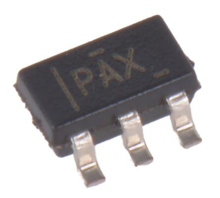
| 产品图片 |
|
| rohs | 符合RoHS无铅 / 符合限制有害物质指令(RoHS)规范要求 |
| 产品系列 | 电源管理 IC,低压差稳压器,Texas Instruments TLV70450DBVT- |
| 数据手册 | |
| 产品型号 | TLV70450DBVT |
| 产品种类 | 低压差稳压器 |
| 供应商器件封装 | SOT-23-5 |
| 其它名称 | 296-28171-1 |
| 包装 | 剪切带 (CT) |
| 商标 | Texas Instruments |
| 回动电压—最大值 | 1.1 V |
| 安装类型 | 表面贴装 |
| 安装风格 | SMD/SMT |
| 封装 | Reel |
| 封装/外壳 | SC-74A,SOT-753 |
| 封装/箱体 | SOT-23-5 |
| 工作温度 | -40°C ~ 125°C |
| 工厂包装数量 | 250 |
| 最大功率耗散 | 470 mW |
| 最大工作温度 | + 125 C |
| 最大输入电压 | 24 V |
| 标准包装 | 1 |
| 电压-跌落(典型值) | 0.85V @ 100mA |
| 电压-输入 | 最高 24V |
| 电压-输出 | 5V |
| 电压调节准确度 | 2 % |
| 电流-输出 | 150mA |
| 电流-限制(最小值) | 160mA |
| 稳压器拓扑 | 正,固定式 |
| 稳压器数 | 1 |
| 系列 | TLV70450 |
| 负载调节 | 33 mV |
| 输出电压 | 5 V |
| 输出电流 | 1 mA |
| 输出端数量 | 1 Output |
| 输出类型 | Fixed |


PDF Datasheet 数据手册内容提取
Product Sample & Technical Tools & Support & Folder Buy Documents Software Community TLV704 SBVS148D–OCTOBER2010–REVISEDJANUARY2015 TLV704 24-V Input Voltage, 150-mA, Ultralow I Low-Dropout Regulators Q 1 Features 3 Description • WideInputVoltageRange:2.5Vto24V The TLV704 series of low-dropout (LDO) regulators 1 are ultralow quiescent current devices designed for • Low3.2-μAQuiescentCurrent extremely power-sensitive applications. Quiescent • GroundPinCurrent:3.4 μAat100-mAIOUT current is virtually constant over the complete load • StableWithaLow-ESR,1-µFTypicalOutput current and ambient temperature range. These Capacitor devices are an ideal power-management attachment tolow-powermicrocontrollers,suchastheMSP430. • OperatingJunctionTemperature: –40°Cto125°C The TLV704 operates over a wide operating input voltage of 2.5 V to 24 V. Thus, the device is an • AvailableinSOT23-5Package excellent choice for both battery-powered systems as – SeePackageOptionAddendumatendofthis well as industrial applications that undergo large line documentforcompletelistofavailablevoltage transients. options The TLV704 is available in a 3-mm × 3-mm SOT23-5 package, which is ideal for cost-effective board 2 Applications manufacturing. • UltralowPowerMicrocontrollers • E-Meters DeviceInformation(1) • FireAlarmsandSmokeDetectorSystems PARTNUMBER PACKAGE BODYSIZE(nom) TLV704 SOT-23(5) 2.90mmx1.60mm • HandsetPeripherals • IndustrialandAutomotiveApplications (1) For all available packages, see the orderable addendum at theendofthedatasheet. • RemoteControllers • Zigbee®Networks • Portable,Battery-PoweredEquipment TypicalApplication TLV70433 V IN OUT MSP430 IN GND 0.1mF 1mF 1 An IMPORTANT NOTICE at the end of this data sheet addresses availability, warranty, changes, use in safety-critical applications, intellectualpropertymattersandotherimportantdisclaimers.PRODUCTIONDATA.
TLV704 SBVS148D–OCTOBER2010–REVISEDJANUARY2015 www.ti.com Table of Contents 1 Features.................................................................. 1 8 ApplicationandImplementation........................ 12 2 Applications........................................................... 1 8.1 ApplicationInformation............................................12 3 Description............................................................. 1 8.2 TypicalApplication..................................................12 4 RevisionHistory..................................................... 2 9 PowerSupplyRecommendations...................... 13 5 PinConfigurationandFunctions......................... 4 10 Layout................................................................... 13 6 Specifications......................................................... 5 10.1 LayoutGuidelines.................................................13 6.1 AbsoluteMaximumRatings .....................................5 10.2 LayoutExample....................................................13 6.2 ESDRatings ............................................................5 10.3 PowerDissipationandJunctionTemperature......14 6.3 RecommendedOperatingConditions.......................5 10.4 EstimatingJunctionTemperature.........................14 6.4 ThermalInformation..................................................5 10.5 PackageMounting................................................14 6.5 ElectricalCharacteristics...........................................6 11 DeviceandDocumentationSupport................. 15 6.6 TypicalCharacteristics..............................................7 11.1 DeviceSupport ....................................................15 7 DetailedDescription............................................ 10 11.2 DocumentationSupport........................................15 7.1 Overview.................................................................10 11.3 Trademarks...........................................................15 7.2 FunctionalBlockDiagram.......................................10 11.4 ElectrostaticDischargeCaution............................15 7.3 FeatureDescription.................................................10 11.5 Glossary................................................................15 7.4 DeviceFunctionalModes........................................11 12 Mechanical,Packaging,andOrderable Information........................................................... 15 4 Revision History NOTE:Pagenumbersforpreviousrevisionsmaydifferfrompagenumbersinthecurrentversion. ChangesfromRevisionC(August,2011)toRevisionD Page • AddedESDRatingstable,FeatureDescriptionsection,DeviceFunctionalModes,ApplicationandImplementation section,PowerSupplyRecommendationssection,Layoutsection,DeviceandDocumentationSupportsection,and Mechanical,Packaging,andOrderableInformationsection.................................................................................................. 1 • ChangedfourthbulletinFeatureslist.................................................................................................................................... 1 • ChangedApplicationslist ...................................................................................................................................................... 1 • Changedfront-pagefigure;removedpinout........................................................................................................................... 1 • ChangedPinConfigurationandFunctionssection;updatedtableformat,renamedpinpackagetomeetnew standards ............................................................................................................................................................................... 4 • Changed"free-air"to"junction"temperatureinconditionstatementforAbsoluteMaximumRatings .................................. 5 • Changed"free-air"to"junction"temperatureinconditionstatementforRecommendedOperatingConditions ...................5 • DeletedPowerDissipationRatingtable................................................................................................................................. 5 • Changed"T "to"T"inconditionstatementforElectricalCharacteristics............................................................................ 6 A J • Changedparametricsymbolforlineregulation ..................................................................................................................... 6 • Changedparametricsymbolforloadregulation.................................................................................................................... 6 ChangesfromRevisionB(November,2010)toRevisionC Page • ReviseddocumenttoreflectPKpackageoptionremoval...................................................................................................... 1 • RemovedSOT89(PK)packagefromfront-pagefigure......................................................................................................... 1 • DeletedPKpackageinformationfromPinFunctionstable ................................................................................................... 4 • RevisedThermalInformationtableandPowerDissipationRatingtable .............................................................................. 5 • AddedloadregulationspecificationsforV ≥3.3V............................................................................................................ 6 OUT • RemovedFigure15andFigure16....................................................................................................................................... 14 2 SubmitDocumentationFeedback Copyright©2010–2015,TexasInstrumentsIncorporated ProductFolderLinks:TLV704
TLV704 www.ti.com SBVS148D–OCTOBER2010–REVISEDJANUARY2015 ChangesfromRevisionA(October,2010)toRevisionB Page • UpdateddocumenttoreflectavailabilityofPKpackageoption............................................................................................. 1 • Correctedtypoinfront-pagefigure......................................................................................................................................... 1 • ChangedPinFunctionstabletocorrectpinnumberingforPKpackageoption..................................................................... 4 • RevisedTypicalCharacteristicssection;addedandremovedgraphs................................................................................... 7 • UpdatedformatofApplicationInformationsection............................................................................................................... 10 Copyright©2010–2015,TexasInstrumentsIncorporated SubmitDocumentationFeedback 3 ProductFolderLinks:TLV704
TLV704 SBVS148D–OCTOBER2010–REVISEDJANUARY2015 www.ti.com 5 Pin Configuration and Functions DBVPackage SOT-23(5) (TopView) GND 1 5 NC IN 2 OUT 3 4 NC PinFunctions PIN I/O DESCRIPTION NAME NO. GND 1 — Ground IN 2 I Unregulatedinputvoltage. OUT 3 O Regulatedoutputvoltage.Anycapacitorgreaterthan1µFbetweenthispinandgroundisneededforstability. NC 4,5 — Notinternallyconnected.Thispincanbeleftopenortiedtogroundforimprovedthermalperformance. 4 SubmitDocumentationFeedback Copyright©2010–2015,TexasInstrumentsIncorporated ProductFolderLinks:TLV704
TLV704 www.ti.com SBVS148D–OCTOBER2010–REVISEDJANUARY2015 6 Specifications 6.1 Absolute Maximum Ratings Overoperatingjunctiontemperaturerange,unlessotherwisenoted(1). MIN MAX UNIT Voltage(2) IN –0.3 24 V Currentsource OUT Internallylimited Operatingjunction,T –40 150 °C J Temperature Storagerange,T –65 150 °C stg (1) StressesbeyondthoselistedunderAbsoluteMaximumRatingsmaycausepermanentdamagetothedevice.Thesearestressratings only,andfunctionaloperationofthedeviceattheseoranyotherconditionsbeyondthoseindicatedunderRecommendedOperating Conditionsisnotimplied.Exposuretoabsolute-maximum-ratedconditionsforextendedperiodsmyaffectdevicereliability. (2) Allvoltagesarewithrespecttonetworkgroundterminal. 6.2 ESD Ratings VALUE UNIT Humanbodymodel(HBM),perANSI/ESDA/JEDECJS-001,allpins(1) ±2000 V(ESD) Electrostaticdischarge Chargeddevicemodel(CDM),perJEDECspecificationJESD22-C101, V allpins(2) ±500 (1) JEDECdocumentJEP155statesthat500-VHBMallowssafemanufacturingwithastandardESDcontrolprocess. (2) JEDECdocumentJEP157statesthat250-VCDMallowssafemanufacturingwithastandardESDcontrolprocess. 6.3 Recommended Operating Conditions overoperatingjunctiontemperaturerange(unlessotherwisenoted) MIN NOM MAX UNIT V Inputvoltage 2.5 24 V IN I Outputcurrent 0 150 mA OUT T Operatingjunctiontemperature –40 125 °C J 6.4 Thermal Information TLV704 THERMALMETRIC(1) DBV UNIT 5PINS R Junction-to-ambientthermalresistance 213.1 θJA R Junction-to-case(top)thermalresistance 110.9 θJC(top) R Junction-to-boardthermalresistance 97.4 °C/W θJB ψ Junction-to-topcharacterizationparameter 22.0 JT ψ Junction-to-boardcharacterizationparameter 78.4 JB (1) Formoreinformationabouttraditionalandnewthermalmetrics,seetheICPackageThermalMetricsapplicationreport,SPRA953. Copyright©2010–2015,TexasInstrumentsIncorporated SubmitDocumentationFeedback 5 ProductFolderLinks:TLV704
TLV704 SBVS148D–OCTOBER2010–REVISEDJANUARY2015 www.ti.com 6.5 Electrical Characteristics AllvaluesareatT =25°C,V =V +1V,I =1mA,andC =1µF,unlessotherwisenoted. J IN OUT(nom) OUT OUT PARAMETER TESTCONDITIONS MIN TYP MAX UNIT V Inputvoltagerange 24 V IN Outputvoltagerange 1.2 5 V V DCoutputaccuracy –2% 2% OUT ΔV Lineregulation V +1V<V <24V 20 50 mV O(ΔVI) (nom) IN 0mA<I <10mA 10 OUT V ≤3.3V 0mA<I <50mA 25 OUT OUT 0mA<I <100mA 33 50 OUT ΔV Loadregulation mV O(ΔIO) 0mA<I <10mA 7 OUT V ≥3.3V 0mA<I <50mA 35 OUT OUT 0mA<I <100mA 50 75 OUT I =10mA 75 OUT V Dropoutvoltage(1) I =50mA 400 mV DO OUT I =100mA 850 1100 OUT I Outputcurrentlimit V =0V 160 1000 mA CL OUT I =0mA 3.2 4.5 OUT I Groundpincurrent µA GND I =100mA 3.4 5.5 OUT Power-supplyrejection PSRR f=100kHz,C =10µF 60 dB ratio OUT Operatingjunction T –40 125 °C J temperature (1) V =V –0.1V. IN OUT(nom) 6 SubmitDocumentationFeedback Copyright©2010–2015,TexasInstrumentsIncorporated ProductFolderLinks:TLV704
TLV704 www.ti.com SBVS148D–OCTOBER2010–REVISEDJANUARY2015 6.6 Typical Characteristics 3.4 3.6 V = 3.3 V 3.38 OUT I = 5 mA OUT 3.5 3.36 ge (V) 33..3342 ge (V) 3.4 a a olt 3.3 olt 3.3 V V ut 3.28 ut p p Out 3.26 Out 3.2 3.24 -40°C 3.1 -40°C 3.22 +25°C +25°C +85°C +85°C 3.2 3 4 8 12 16 20 24 0 30 60 90 120 150 Input Voltage (V) Output Current (mA) Figure1.LineRegulation Figure2.LoadRegulation(V =3.3V) OUT 3.465 120 3.432 VIN= 4.3 V IOUT= 10 mA 100 3.399 Voltage (V) 33..33363.633 IOUT= 10 mA Voltage (mV) 8600 Output 333...222630741 IOUT= 80 mA Dropout 40 -40°C 20 +25°C 3.168 +85°C 3.135 0 -40 -25 -10 5 20 35 50 65 80 95 110 125 2.5 2.6 2.7 2.8 2.9 3 3.1 3.2 3.3 Junction Temperature (°C) Input Voltage (V) Figure3.OutputVoltagevsJunctionTemperature Figure4.DropoutVoltagevsInputVoltage(TLV70433) 2100 4.5 V = 4.3 V IN 1800 VOUT= 3.3 V 4 I = 1mF V) 1500 A) OUT m m Voltage ( 1200 Current ( 3.5 Dropout 960000 Ground 3 -40°C 2.5 300 +25°C +85°C 0 2 0 30 60 90 120 150 -40 -25 -10 5 20 35 50 65 80 95 110 125 Output Current (mA) Junction Temperature (°C) Figure5.DropoutVoltagevsOutputCurrent Figure6.GroundCurrentvsJunctionTemperature Copyright©2010–2015,TexasInstrumentsIncorporated SubmitDocumentationFeedback 7 ProductFolderLinks:TLV704
TLV704 SBVS148D–OCTOBER2010–REVISEDJANUARY2015 www.ti.com Typical Characteristics (continued) 4.5 4.5 VOUT= 3.3 V VOUT= 3.3 V 4 4 A) 3.5 A) 3.5 m m nt ( 3 nt ( 3 e e urr 2.5 urr 2.5 C C Pin 2 Pin 2 nd 1.5 nd 1.5 u u o o Gr 1 -40°C Gr 1 -40°C 0.5 +25°C 0.5 +25°C +85°C +85°C 0 0 3 6 9 12 15 18 21 24 0 30 60 90 120 150 Input Voltage (V) Output Current (mA) Figure7.GroundPinCurrentvsInputVoltage Figure8.GroundPinCurrentvsLoadCurrent 250 8 200 VOUT= 3.3 V,- V40IN°C= 4.8 V +25°C +85°C m?y (V/)Hz 76 IOUT= 1 mA VCOVOUIUNTT=== 43 1..33m VVF mit (mA) 150 e Densit 5 IOUT= 50 mA Current Li 100 ctral Nois 43 pe 2 50 S put 1 ut 0 O 0 Temperature (°C) 100 1 k 10 k 100 k Frequency (Hz) Figure9.CurrentLimitvsJunctionTemperature Figure10.OutputSpectralNoiseDensityvsFrequency 100 8 er-Supply Rejection Ratio (dB) 9876543200000000 VVCTJIOONU=U=TT + ==42 . 5331°. 03VC mVF IOUT= I1O UmTA= 50 mA Input Voltage (V)Output Voltage (V) 765432 VCROOLUU=VTT 6I=N=6 31W.03 mVFVOUT w Po 10 1 0 0 10 100 1 k 10 k 100 k 1 M 10 M Time (2 ms/div) Frequency (Hz) Figure11.Power-SupplyRippleRejectionvsFrequency Figure12.PowerUp/PowerDown 8 SubmitDocumentationFeedback Copyright©2010–2015,TexasInstrumentsIncorporated ProductFolderLinks:TLV704
TLV704 www.ti.com SBVS148D–OCTOBER2010–REVISEDJANUARY2015 Typical Characteristics (continued) Output Voltage (mV) 1-0550000 CIOOUVUTITN=== 5 1300. 3mm AVF Output Voltage (mV)-2200000 VVCIOONUU=TT ==4 . 331. 03V mVF V) mA) oltage ( 5.3 urrent ( 10500 V C put 4.3 put 0 In Time (50 ms/div) Out Time (0.5 ms/div) Figure13.LineTransientResponse Figure14.LoadTransientResponse Copyright©2010–2015,TexasInstrumentsIncorporated SubmitDocumentationFeedback 9 ProductFolderLinks:TLV704
TLV704 SBVS148D–OCTOBER2010–REVISEDJANUARY2015 www.ti.com 7 Detailed Description 7.1 Overview The TLV704 series belong to a family of ultralow I LDO regulators. I remains fairly constant over the complete Q Q output load current and temperature range. The devices are ensured to operate over a temperature range of –40°Cto125°C. 7.2 Functional Block Diagram V V IN OUT Current Sense I LIM R _ 1 + GND R V = 1.205 V 2 REF Bandgap Reference R = 840 kW 2 7.3 Feature Description 7.3.1 RegulatorProtection The TLV704 series of LDO regulators use a PMOS-pass transistor that has a built-in back diode that conducts reversecurrentwhentheinputvoltagedropsbelowtheoutputvoltage(forexample,duringpowerdown).Current is conducted from the output to the input and is not internally limited. If extended reverse voltage operation is anticipated,externallimitingisappropriate. The TLV704 features internal current limiting. During normal operation, the TLV704 limits output current to approximately 250 mA. When current limiting engages, the output voltage scales back linearly until the overcurrent condition ends. Do not exceed the rated maximum operating junction temperature of 125°C. Continuously running the device under conditions where the junction temperature exceeds 125°C degrades devicereliability. The ability to remove heat from the die is different for each package type, presenting different considerations in the printed circuit board (PCB) layout. The PCB area around the device that is free of other components moves theheatfromthedevicetotheambientair.PerformancedataforJEDEChigh-KboardsaregivenintheThermal Information table. Using heavier copper increases the effectiveness in removing heat from the device. The addition of plated through-holes to heat-dissipating layers also improves heatsink effectiveness. Power dissipation depends on input voltage and load conditions. Power dissipation (P ) is equal to the product of the D outputcurrentandthevoltagedropacrosstheoutputpasselement,asshowninEquation2. 10 SubmitDocumentationFeedback Copyright©2010–2015,TexasInstrumentsIncorporated ProductFolderLinks:TLV704
TLV704 www.ti.com SBVS148D–OCTOBER2010–REVISEDJANUARY2015 7.4 Device Functional Modes 7.4.1 NormalOperation Thedeviceregulatestothenominaloutputvoltageunderthefollowingconditions: • Theinputvoltageisgreaterthanthenominaloutputvoltageaddedtothedropoutvoltage. • Theoutputcurrentislessthanthecurrentlimit. 7.4.2 DropoutOperation If the input voltage is lower than the nominal output voltage plus the specified dropout voltage, but all other conditions are met for normal operation, the device operates in dropout mode. In this condition, the output voltage is the same the input voltage minus the dropout voltage. The transient performance of the device is significantly degraded because the pass device is in a triode state and no longer controls the current through the LDO.Lineorloadtransientsindropoutmayresultinlargeoutputvoltagedeviations. Table1liststheconditionsthatleadtothedifferentmodesofoperation. Table1.DeviceFunctionalModeComparison PARAMETER OPERATINGMODE V I IN OUT Normalmode V >V +V I <I IN OUT(nom) DO OUT CL Dropoutmode V <V +V I <I IN OUT(nom) DO OUT CL Copyright©2010–2015,TexasInstrumentsIncorporated SubmitDocumentationFeedback 11 ProductFolderLinks:TLV704
TLV704 SBVS148D–OCTOBER2010–REVISEDJANUARY2015 www.ti.com 8 Application and Implementation NOTE Information in the following applications sections is not part of the TI component specification, and TI does not warrant its accuracy or completeness. TI’s customers are responsible for determining suitability of components for their purposes. Customers should validateandtesttheirdesignimplementationtoconfirmsystemfunctionality. 8.1 Application Information The TLV704 family of LDOs are designed for power-sensitive applications and feature low quiescent current. Thesedevicespairwellwithlow-powermicrocontrollers,suchastheMSP430. 8.2 Typical Application TLV70433 V IN OUT MSP430 IN GND 0.1mF 1mF Figure15. TypicalApplication 8.2.1 DesignRequirements Selectthedesireddevicebasedontheoutputvoltage. Provide an input supply with adequate headroom to account for dropout and output current to account for the GNDterminalcurrent,andpowertheload. 8.2.2 DetailedDesignProcedure 8.2.2.1 InputandOutputCapacitorRequirements The TLV704 requires a 1-µF or larger capacitor connected between OUT and GND for stability. Ceramic or tantalumcapacitorscanbeused.Largervaluecapacitorsresultinbettertransientandnoiseperformance. Although an input capacitor is not required for stability, when a 0.1-µF or larger capacitor is placed between IN and GND, it counteracts reactive input sources and improves transient and noise performance. Higher value capacitorsarenecessaryiflarge,fastrisetimeloadtransientsareanticipated. 12 SubmitDocumentationFeedback Copyright©2010–2015,TexasInstrumentsIncorporated ProductFolderLinks:TLV704
TLV704 www.ti.com SBVS148D–OCTOBER2010–REVISEDJANUARY2015 Typical Application (continued) 8.2.3 ApplicationCurves 100 8 er-Supply Rejection Ratio (dB) 9876543200000000 VVCTJIOONU=U=TT + ==42 . 5331°. 03VC mVF IOUT= I1O UmTA= 50 mA Input Voltage (V)Output Voltage (V) 765432 VCROOLUU=VTT 6I=N=6 31W.03 mVFVOUT w Po 10 1 0 0 10 100 1 k 10 k 100 k 1 M 10 M Time (2 ms/div) Frequency (Hz) Figure16.Power-SupplyRippleRejectionvsFrequency Figure17.PowerUp/PowerDown 9 Power Supply Recommendations Connect a low output impedance power supply directly to the IN pin of the TLV704. Inductive impedances between the input supply and the IN pin can create significant voltage excursions at the IN pin during start-up or loadtransientevents.Ifinductiveimpedancesareunavoidable,useaninputcapacitor. 10 Layout 10.1 Layout Guidelines Input and output capacitors should be placed as close to the device pins as possible. To avoid interference of noise and ripple on the board, TI recommends designing the board with separate ground planes for V and IN V , with the ground plane connected only at the device GND pin. In addition, the ground connection for the OUT outputcapacitorshouldbeconnecteddirectlytothedeviceGNDpin. 10.2 Layout Example VOUT VIN CIN COUT GND PLANE Figure18. LayoutExamplefortheDBVPackage Copyright©2010–2015,TexasInstrumentsIncorporated SubmitDocumentationFeedback 13 ProductFolderLinks:TLV704
TLV704 SBVS148D–OCTOBER2010–REVISEDJANUARY2015 www.ti.com 10.3 Power Dissipation and Junction Temperature Toensurereliableoperation,worst-casejunctiontemperatureshouldnotexceed125°C.Thisrestrictionlimitsthe power dissipation the regulator can handle in any given application. To ensure the junction temperature is within acceptable limits, calculate the maximum allowable dissipation, P , and the actual dissipation, P , which D(max) D mustbelessthanorequaltoP . D(max) ThemaximumpowerdissipationlimitisdeterminedusingEquation1: T -T P = Jmax A D(max) R qJA (1) where: T isthemaximumallowablejunctiontemperature. Jmax R isthethermalresistancejunction-to-ambientforthepackage(seetheThermalInformation table). θJA T istheambienttemperature. A TheregulatordissipationiscalculatedusingEquation2: P =(V -V )´I D IN OUT OUT (2) Powerdissipationresultingfromquiescentcurrentisnegligible. 10.4 Estimating Junction Temperature The JEDEC standard now recommends the use of psi (Ψ) thermal metrics to estimate the junction temperatures of the LDO while in-circuit on a typical PCB board application. These metrics are not strictly speaking thermal resistances, but rather offer practical and relative means of estimating junction temperatures. These psi metrics are determined to be significantly independent of the copper-spreading area. The key thermal metrics (Ψ and JT Ψ )aregivenintheThermalInformationtableandareusedinaccordancewithEquation3. JB Y :T =T +Y ´P JT J T JT D Y :T =T +Y ´P JB J B JB D where: • P isthepowerdissipatedasexplainedinThermalInformation D • T isthetemperatureatthecenter-topofthedevicepackage T • T isthePCBsurfacetemperaturemeasured1mmfromthedevicepackageandcenteredonthepackage B edge. (3) 10.5 Package Mounting Solder pad footprint recommendations for the TLV704 are available from the TI's website at www.ti.com through theTLV704seriesproductfolders.TherecommendedlandpatternfortheDBVpackageisappendedtothisdata sheet. 14 SubmitDocumentationFeedback Copyright©2010–2015,TexasInstrumentsIncorporated ProductFolderLinks:TLV704
TLV704 www.ti.com SBVS148D–OCTOBER2010–REVISEDJANUARY2015 11 Device and Documentation Support 11.1 Device Support 11.1.1 DevelopmentSupport 11.1.1.1 EvaluationModule An evaluation module (EVM) is available to assist in the initial circuit performance evaluation using the TLV704. The TLV70433DBVEVM-712 evaluation module (and related user guide) can be requested at the Texas InstrumentswebsitethroughtheproductfoldersorpurchaseddirectlyfromtheTIeStore. 11.1.2 DeviceNomenclature Table2.AvailableOptions(1) PRODUCT V OUT xxisnominaloutputvoltage(forexample33=3.3V) TLV704xxyyyz yyyisPackageDesignator zisPackageQuantity (1) Forthemostcurrentpackageandorderinginformation,seethePackageOptionAddendumattheendofthisdocument,orvisitthe deviceproductfolderatwww.ti.com. 11.2 Documentation Support 11.2.1 RelatedDocumentation • TLV70433DBVEVM-712,TLV70433PKEVM-712EvaluationModules,SBVU017 11.3 Trademarks ZigbeeisaregisteredtrademarkofZigBeeAlliance. Allothertrademarksarethepropertyoftheirrespectiveowners. 11.4 Electrostatic Discharge Caution Thesedeviceshavelimitedbuilt-inESDprotection.Theleadsshouldbeshortedtogetherorthedeviceplacedinconductivefoam duringstorageorhandlingtopreventelectrostaticdamagetotheMOSgates. 11.5 Glossary SLYZ022—TIGlossary. Thisglossarylistsandexplainsterms,acronyms,anddefinitions. 12 Mechanical, Packaging, and Orderable Information The following pages include mechanical, packaging, and orderable information. This information is the most current data available for the designated devices. This data is subject to change without notice and revision of thisdocument.Forbrowser-basedversionsofthisdatasheet,refertotheleft-handnavigation. Copyright©2010–2015,TexasInstrumentsIncorporated SubmitDocumentationFeedback 15 ProductFolderLinks:TLV704
PACKAGE OPTION ADDENDUM www.ti.com 28-Jul-2016 PACKAGING INFORMATION Orderable Device Status Package Type Package Pins Package Eco Plan Lead/Ball Finish MSL Peak Temp Op Temp (°C) Device Marking Samples (1) Drawing Qty (2) (6) (3) (4/5) TLV70430DBVR ACTIVE SOT-23 DBV 5 3000 Green (RoHS CU NIPDAU Level-1-260C-UNLIM -40 to 125 QUQ & no Sb/Br) TLV70430DBVT ACTIVE SOT-23 DBV 5 250 Green (RoHS CU NIPDAU Level-1-260C-UNLIM -40 to 125 QUQ & no Sb/Br) TLV70433DBVR ACTIVE SOT-23 DBV 5 3000 Green (RoHS CU NIPDAU Level-1-260C-UNLIM -40 to 125 PAO & no Sb/Br) TLV70433DBVT ACTIVE SOT-23 DBV 5 250 Green (RoHS CU NIPDAU Level-1-260C-UNLIM -40 to 125 PAO & no Sb/Br) TLV704345DBVR ACTIVE SOT-23 DBV 5 3000 Green (RoHS CU NIPDAU Level-1-260C-UNLIM -40 to 125 13T & no Sb/Br) TLV704345DBVT ACTIVE SOT-23 DBV 5 250 Green (RoHS CU NIPDAU Level-1-260C-UNLIM -40 to 125 13T & no Sb/Br) TLV70436DBVR ACTIVE SOT-23 DBV 5 3000 Green (RoHS CU NIPDAU Level-1-260C-UNLIM -40 to 125 PAW & no Sb/Br) TLV70436DBVT ACTIVE SOT-23 DBV 5 250 Green (RoHS CU NIPDAU Level-1-260C-UNLIM -40 to 125 PAW & no Sb/Br) TLV70450DBVR ACTIVE SOT-23 DBV 5 3000 Green (RoHS CU NIPDAU Level-1-260C-UNLIM -40 to 125 PAX & no Sb/Br) TLV70450DBVT ACTIVE SOT-23 DBV 5 250 Green (RoHS CU NIPDAU Level-1-260C-UNLIM -40 to 125 PAX & no Sb/Br) (1) The marketing status values are defined as follows: ACTIVE: Product device recommended for new designs. LIFEBUY: TI has announced that the device will be discontinued, and a lifetime-buy period is in effect. NRND: Not recommended for new designs. Device is in production to support existing customers, but TI does not recommend using this part in a new design. PREVIEW: Device has been announced but is not in production. Samples may or may not be available. OBSOLETE: TI has discontinued the production of the device. (2) Eco Plan - The planned eco-friendly classification: Pb-Free (RoHS), Pb-Free (RoHS Exempt), or Green (RoHS & no Sb/Br) - please check http://www.ti.com/productcontent for the latest availability information and additional product content details. TBD: The Pb-Free/Green conversion plan has not been defined. Pb-Free (RoHS): TI's terms "Lead-Free" or "Pb-Free" mean semiconductor products that are compatible with the current RoHS requirements for all 6 substances, including the requirement that lead not exceed 0.1% by weight in homogeneous materials. Where designed to be soldered at high temperatures, TI Pb-Free products are suitable for use in specified lead-free processes. Pb-Free (RoHS Exempt): This component has a RoHS exemption for either 1) lead-based flip-chip solder bumps used between the die and package, or 2) lead-based die adhesive used between the die and leadframe. The component is otherwise considered Pb-Free (RoHS compatible) as defined above. Green (RoHS & no Sb/Br): TI defines "Green" to mean Pb-Free (RoHS compatible), and free of Bromine (Br) and Antimony (Sb) based flame retardants (Br or Sb do not exceed 0.1% by weight in homogeneous material) Addendum-Page 1
PACKAGE OPTION ADDENDUM www.ti.com 28-Jul-2016 (3) MSL, Peak Temp. - The Moisture Sensitivity Level rating according to the JEDEC industry standard classifications, and peak solder temperature. (4) There may be additional marking, which relates to the logo, the lot trace code information, or the environmental category on the device. (5) Multiple Device Markings will be inside parentheses. Only one Device Marking contained in parentheses and separated by a "~" will appear on a device. If a line is indented then it is a continuation of the previous line and the two combined represent the entire Device Marking for that device. (6) Lead/Ball Finish - Orderable Devices may have multiple material finish options. Finish options are separated by a vertical ruled line. Lead/Ball Finish values may wrap to two lines if the finish value exceeds the maximum column width. Important Information and Disclaimer:The information provided on this page represents TI's knowledge and belief as of the date that it is provided. TI bases its knowledge and belief on information provided by third parties, and makes no representation or warranty as to the accuracy of such information. Efforts are underway to better integrate information from third parties. TI has taken and continues to take reasonable steps to provide representative and accurate information but may not have conducted destructive testing or chemical analysis on incoming materials and chemicals. TI and TI suppliers consider certain information to be proprietary, and thus CAS numbers and other limited information may not be available for release. In no event shall TI's liability arising out of such information exceed the total purchase price of the TI part(s) at issue in this document sold by TI to Customer on an annual basis. Addendum-Page 2
PACKAGE MATERIALS INFORMATION www.ti.com 30-Nov-2016 TAPE AND REEL INFORMATION *Alldimensionsarenominal Device Package Package Pins SPQ Reel Reel A0 B0 K0 P1 W Pin1 Type Drawing Diameter Width (mm) (mm) (mm) (mm) (mm) Quadrant (mm) W1(mm) TLV70430DBVR SOT-23 DBV 5 3000 178.0 9.0 3.23 3.17 1.37 4.0 8.0 Q3 TLV70430DBVT SOT-23 DBV 5 250 178.0 8.4 3.23 3.17 1.37 4.0 8.0 Q3 TLV70433DBVR SOT-23 DBV 5 3000 178.0 9.0 3.23 3.17 1.37 4.0 8.0 Q3 TLV70433DBVT SOT-23 DBV 5 250 178.0 8.4 3.23 3.17 1.37 4.0 8.0 Q3 TLV704345DBVR SOT-23 DBV 5 3000 178.0 9.0 3.23 3.17 1.37 4.0 8.0 Q3 TLV704345DBVT SOT-23 DBV 5 250 178.0 8.4 3.23 3.17 1.37 4.0 8.0 Q3 TLV70436DBVR SOT-23 DBV 5 3000 178.0 9.0 3.23 3.17 1.37 4.0 8.0 Q3 TLV70436DBVT SOT-23 DBV 5 250 178.0 8.4 3.23 3.17 1.37 4.0 8.0 Q3 TLV70450DBVR SOT-23 DBV 5 3000 178.0 9.0 3.23 3.17 1.37 4.0 8.0 Q3 TLV70450DBVT SOT-23 DBV 5 250 178.0 8.4 3.3 3.2 1.4 4.0 8.0 Q3 PackMaterials-Page1
PACKAGE MATERIALS INFORMATION www.ti.com 30-Nov-2016 *Alldimensionsarenominal Device PackageType PackageDrawing Pins SPQ Length(mm) Width(mm) Height(mm) TLV70430DBVR SOT-23 DBV 5 3000 180.0 180.0 18.0 TLV70430DBVT SOT-23 DBV 5 250 180.0 180.0 18.0 TLV70433DBVR SOT-23 DBV 5 3000 180.0 180.0 18.0 TLV70433DBVT SOT-23 DBV 5 250 180.0 180.0 18.0 TLV704345DBVR SOT-23 DBV 5 3000 180.0 180.0 18.0 TLV704345DBVT SOT-23 DBV 5 250 180.0 180.0 18.0 TLV70436DBVR SOT-23 DBV 5 3000 180.0 180.0 18.0 TLV70436DBVT SOT-23 DBV 5 250 180.0 180.0 18.0 TLV70450DBVR SOT-23 DBV 5 3000 180.0 180.0 18.0 TLV70450DBVT SOT-23 DBV 5 250 180.0 180.0 18.0 PackMaterials-Page2
PACKAGE OUTLINE DBV0005A SOT-23 - 1.45 mm max height SCALE 4.000 SMALL OUTLINE TRANSISTOR C 3.0 2.6 0.1 C 1.75 1.45 B A 1.45 MAX PIN 1 INDEX AREA 1 5 2X 0.95 3.05 2.75 1.9 1.9 2 4 3 0.5 5X 0.3 0.15 0.2 C A B (1.1) TYP 0.00 0.25 GAGE PLANE 0.22 TYP 0.08 8 TYP 0.6 0 0.3 TYP SEATING PLANE 4214839/D 11/2018 NOTES: 1. All linear dimensions are in millimeters. Any dimensions in parenthesis are for reference only. Dimensioning and tolerancing per ASME Y14.5M. 2. This drawing is subject to change without notice. 3. Refernce JEDEC MO-178. 4. Body dimensions do not include mold flash, protrusions, or gate burrs. Mold flash, protrusions, or gate burrs shall not exceed 0.15 mm per side. www.ti.com
EXAMPLE BOARD LAYOUT DBV0005A SOT-23 - 1.45 mm max height SMALL OUTLINE TRANSISTOR PKG 5X (1.1) 1 5 5X (0.6) SYMM (1.9) 2 2X (0.95) 3 4 (R0.05) TYP (2.6) LAND PATTERN EXAMPLE EXPOSED METAL SHOWN SCALE:15X SOLDER MASK SOLDER MASK METAL UNDER METAL OPENING OPENING SOLDER MASK EXPOSED METAL EXPOSED METAL 0.07 MAX 0.07 MIN ARROUND ARROUND NON SOLDER MASK SOLDER MASK DEFINED DEFINED (PREFERRED) SOLDER MASK DETAILS 4214839/D 11/2018 NOTES: (continued) 5. Publication IPC-7351 may have alternate designs. 6. Solder mask tolerances between and around signal pads can vary based on board fabrication site. www.ti.com
EXAMPLE STENCIL DESIGN DBV0005A SOT-23 - 1.45 mm max height SMALL OUTLINE TRANSISTOR PKG 5X (1.1) 1 5 5X (0.6) SYMM 2 (1.9) 2X(0.95) 3 4 (R0.05) TYP (2.6) SOLDER PASTE EXAMPLE BASED ON 0.125 mm THICK STENCIL SCALE:15X 4214839/D 11/2018 NOTES: (continued) 7. Laser cutting apertures with trapezoidal walls and rounded corners may offer better paste release. IPC-7525 may have alternate design recommendations. 8. Board assembly site may have different recommendations for stencil design. www.ti.com
IMPORTANTNOTICEANDDISCLAIMER TIPROVIDESTECHNICALANDRELIABILITYDATA(INCLUDINGDATASHEETS),DESIGNRESOURCES(INCLUDINGREFERENCE DESIGNS),APPLICATIONOROTHERDESIGNADVICE,WEBTOOLS,SAFETYINFORMATION,ANDOTHERRESOURCES“ASIS” ANDWITHALLFAULTS,ANDDISCLAIMSALLWARRANTIES,EXPRESSANDIMPLIED,INCLUDINGWITHOUTLIMITATIONANY IMPLIEDWARRANTIESOFMERCHANTABILITY,FITNESSFORAPARTICULARPURPOSEORNON-INFRINGEMENTOFTHIRD PARTYINTELLECTUALPROPERTYRIGHTS. TheseresourcesareintendedforskilleddevelopersdesigningwithTIproducts.Youaresolelyresponsiblefor(1)selectingtheappropriate TIproductsforyourapplication,(2)designing,validatingandtestingyourapplication,and(3)ensuringyourapplicationmeetsapplicable standards,andanyothersafety,security,orotherrequirements.Theseresourcesaresubjecttochangewithoutnotice.TIgrantsyou permissiontousetheseresourcesonlyfordevelopmentofanapplicationthatusestheTIproductsdescribedintheresource.Other reproductionanddisplayoftheseresourcesisprohibited.NolicenseisgrantedtoanyotherTIintellectualpropertyrightortoanythird partyintellectualpropertyright.TIdisclaimsresponsibilityfor,andyouwillfullyindemnifyTIanditsrepresentativesagainst,anyclaims, damages,costs,losses,andliabilitiesarisingoutofyouruseoftheseresources. TI’sproductsareprovidedsubjecttoTI’sTermsofSale(www.ti.com/legal/termsofsale.html)orotherapplicabletermsavailableeitheron ti.comorprovidedinconjunctionwithsuchTIproducts.TI’sprovisionoftheseresourcesdoesnotexpandorotherwisealterTI’sapplicable warrantiesorwarrantydisclaimersforTIproducts. MailingAddress:TexasInstruments,PostOfficeBox655303,Dallas,Texas75265 Copyright©2019,TexasInstrumentsIncorporated