ICGOO在线商城 > 集成电路(IC) > PMIC - 稳压器 - 线性 > MAX5024MASA+

 Datasheet下载
- 型号: MAX5024MASA+
- 制造商: Maxim
- 库位|库存: xxxx|xxxx
- 要求:
| 数量阶梯 | 香港交货 | 国内含税 |
| +xxxx | $xxxx | ¥xxxx |
查看当月历史价格
查看今年历史价格
MAX5024MASA+产品简介:
ICGOO电子元器件商城为您提供MAX5024MASA+由Maxim设计生产,在icgoo商城现货销售,并且可以通过原厂、代理商等渠道进行代购。 MAX5024MASA+价格参考。MaximMAX5024MASA+封装/规格:PMIC - 稳压器 - 线性, Linear Voltage Regulator IC Positive Fixed or Adjustable 1 Output 5V, 2.5 V ~ 11 V 150mA 8-SOIC。您可以下载MAX5024MASA+参考资料、Datasheet数据手册功能说明书,资料中有MAX5024MASA+ 详细功能的应用电路图电压和使用方法及教程。
MAX5024MASA+ 是由 Maxim Integrated 提供的一款 PMIC(电源管理集成电路),属于线性稳压器类别。该型号的主要应用场景包括:

1. 便携式电子设备:MAX5024MASA+ 适用于需要高效低功耗电源管理的便携式设备,例如智能手机、平板电脑、可穿戴设备(如智能手表和健身追踪器)以及便携式医疗设备。其低静态电流和高精度输出电压特性使其非常适合延长电池寿命。

2. 通信设备:在无线通信模块、路由器、调制解调器等设备中,MAX5024MASA+ 可为射频 (RF) 和基带电路提供稳定的电源供应,确保信号处理的准确性与可靠性。

3. 消费类电子产品:如音频设备、数码相机、游戏控制器等需要稳定电源供应的小型消费类产品中,这款芯片能够提供高效的电源管理方案,同时保持较小的解决方案尺寸。

4. 工业自动化:在工业控制领域,MAX5024MASA+ 可用于传感器接口、数据采集系统及嵌入式控制系统中,为敏感电路提供干净且稳定的电源,减少噪声干扰,提高系统性能。

5. 汽车电子:尽管 MAX5024MASA+ 主要面向消费级市场,但在某些非关键车载应用中(如信息娱乐系统或导航模块),它也可以作为辅助电源使用,为 MCU 或其他外围器件供电。

6. 物联网 (IoT) 设备:对于依赖电池运行的 IoT 节点,例如环境监测传感器或智能家居设备,MAX5024MASA+ 的低功耗特性和紧凑设计非常契合这些设备对长时间续航和小型化的要求。

总之,MAX5024MASA+ 凭借其优异的性能参数,在众多需要高效、低功耗电源管理的应用场景中表现出色,特别适合那些对空间和能耗有严格限制的设计项目。
| 参数 | 数值 |
| 产品目录 | 集成电路 (IC)半导体 |
| 描述 | IC REG LDO 5V/ADJ 0.15A 8SOIC线性稳压器 65V Low-Q w/uP Reset & Watchdog Timer |
| 产品分类 | |
| 品牌 | Maxim Integrated |
| 产品手册 | |
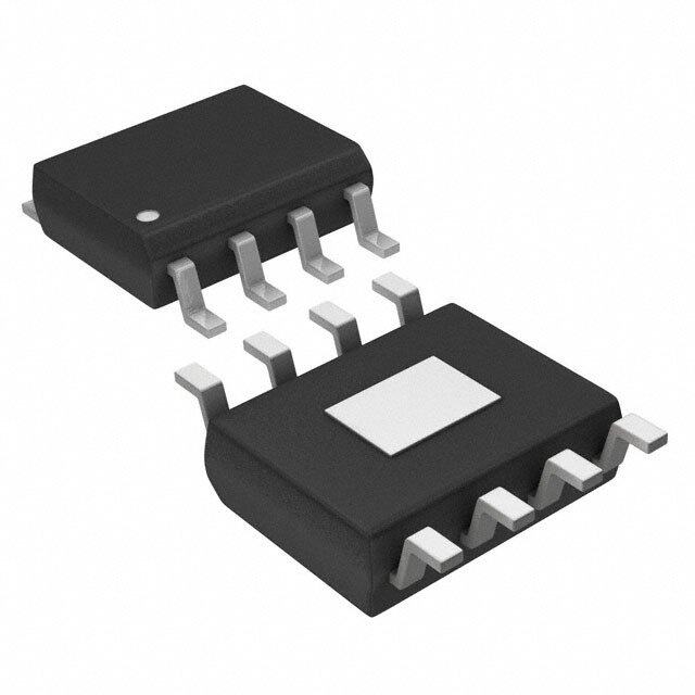
| 产品图片 |
|
| rohs | 符合RoHS无铅 / 符合限制有害物质指令(RoHS)规范要求 |
| 产品系列 | 电源管理 IC,线性稳压器,Maxim Integrated MAX5024MASA+- |
| 数据手册 | |
| 产品型号 | MAX5024MASA+ |
| PSRR/纹波抑制—典型值 | 54 dB |
| 产品培训模块 | http://www.digikey.cn/PTM/IndividualPTM.page?site=cn&lang=zhs&ptm=25703http://www.digikey.cn/PTM/IndividualPTM.page?site=cn&lang=zhs&ptm=25705 |
| 产品种类 | |
| 供应商器件封装 | 8-SOIC N |
| 包装 | 管件 |
| 商标 | Maxim Integrated |
| 安装类型 | 表面贴装 |
| 安装风格 | SMD/SMT |
| 封装 | Tube |
| 封装/外壳 | 8-SOIC(0.154",3.90mm 宽) |
| 封装/箱体 | SO-EP-8 |
| 工作温度 | -40°C ~ 125°C |
| 工厂包装数量 | 100 |
| 应用说明 | |
| 最大功率耗散 | 1538 mW |
| 最大工作温度 | + 125 C |
| 最大输入电压 | 65 V |
| 最小工作温度 | - 40 C |
| 最小输入电压 | 6.5 V |
| 极性 | Positive |
| 标准包装 | 1 |
| 电压-跌落(典型值) | 0.9V @ 150mA |
| 电压-输入 | 6.5 V ~ 65 V |
| 电压-输出 | 5V,2.5 V ~ 11 V |
| 电流-输出 | 150mA |
| 电流-限制(最小值) | - |
| 稳压器拓扑 | 正,固定式或可调式 |
| 稳压器数 | 1 |
| 系列 | MAX5024 |
| 线路调整率 | 1 mV / V |
| 负载调节 | 1 mV / mA |
| 输出电压 | 5 V |
| 输出电流 | 0.15 A |
| 输出端数量 | 1 |
| 输出类型 | Fixed |
| 零件号别名 | MAX5024 |


- 商务部:美国ITC正式对集成电路等产品启动337调查
- 曝三星4nm工艺存在良率问题 高通将骁龙8 Gen1或转产台积电
- 太阳诱电将投资9.5亿元在常州建新厂生产MLCC 预计2023年完工
- 英特尔发布欧洲新工厂建设计划 深化IDM 2.0 战略
- 台积电先进制程称霸业界 有大客户加持明年业绩稳了
- 达到5530亿美元!SIA预计今年全球半导体销售额将创下新高
- 英特尔拟将自动驾驶子公司Mobileye上市 估值或超500亿美元
- 三星加码芯片和SET,合并消费电子和移动部门,撤换高东真等 CEO
- 三星电子宣布重大人事变动 还合并消费电子和移动部门
- 海关总署:前11个月进口集成电路产品价值2.52万亿元 增长14.8%


PDF Datasheet 数据手册内容提取
MAX5023/MAX5024 65V, Low-Quiescent-Current, High-Voltage Linear Regulators with μP Reset and Watchdog Timer General Description Features The MAX5023/MAX5024 high-voltage linear regulators ● Wide Operating Input Voltage Range +6.5V to +65V operate from a +6.5V to +65V input voltage and deliver up ● Thermally Enhanced 8-Pin SO Package with to 150mA of output current. These devices consume only Exposed Pad Dissipates 1.5W 60μA of quiescent current with no load and withstand a -60V reverse-battery voltage at the input. The MAX5023/ ● Guaranteed 150mA Output Current MAX5024 include an active-low internal microprocessor ● 60μA No-Load Supply Current (μP) reset circuit that asserts when the regulator output ● -60V Reverse-Battery Protection drops below the preset output voltage threshold by 7.5% or 12.5%, depending on the device selected. Both devices are ● Preset +3.3V or +5.0V Output Voltage available with a fixed +3.3V or +5V output. These devices ● Thermal and Short-Circuit Protection are short-circuit protected and include thermal shutdown. ● Operate Over -40°C to +125°C Temperature Range In addition to an enable input to turn on or off the regula- ● Integrated μP Reset Circuit tor, the MAX5023/MAX5024 include a HOLD input that allows for the implementation of a self-holding circuit ● Watchdog Timer with 1.6s Timeout Period without requiring external components. Setting HOLD low (MAX5023) after enabling the regulator, forces the regulator to remain ● Regulator Enable and Hold Inputs Implement Self- on even if EN is subsequently set low. Releasing HOLD Holding Circuit shuts down the regulator. ● SET Input for Adjustable Output Voltage (MAX5024) The MAX5023 includes a watchdog input that monitors a pulse train from the μP and generates reset pulses if the watchdog input remains high or low for a duration longer Selector Guide and Ordering Information appear at end of than the 1.6s watchdog timeout period. The MAX5024 data sheet. includes a SET input which, when connected to ground, selects a preset output voltage of +3.3V (MAX5024S/ Typical Operating Circuit MAX5024T) or +5V (MAX5024L/MAX5024M). Set the adjustable output voltage by connecting SET to the regulator’s output through a resistive-divider network. +6.5V TO +65V The MAX5023/MAX5024 operate over the automotive IN OUT VCC temperature range (-40°C to +125°C) and are available in a 10µF 15µF thermally enhanced, surface-mount 8-pin SO-EP package. ONCH MAX5023 µP Applications GNITISWIT 10kΩ I ● Automotive ON RESET RESET OFF EN ● Industrial WDI I/O ● Home Security HOLD I/O ● Fire/Smoke Alarms GND ● Telecom/Networking 19-2619; Rev 8; 3/16
MAX5023/MAX5024 65V, Low-Quiescent-Current, High-Voltage Linear Regulators with μP Reset and Watchdog Timer Absolute Maximum Ratings IN to GND ...............................................................-60V to +70V Continuous Power Dissipation (TA = +70°C) EN to GND .................................................-0.3V to (VIN + 0.3V) 8-Pin SO-EP (derate 19.2mW/°C above +70°C) .......1538mW HOLD to GND ........................................-0.3V to (VOUT + 0.3V) Operating Temperature Range .........................-40°C to +125°C SET, WDI, OUT to GND .....................................-0.3V to +13.2V Junction Temperature ......................................................+150°C RESET to GND (Open Drain) ............................-0.3V to +13.2V Storage Temperature Range ............................-65°C to +150°C Short-Circuit Duration (VIN ≤ +14V) ..........................Continuous Lead Temperature (soldering, 10s) .................................+300°C Maximum Current to Any Pin (Except IN, OUT) ..............±20mA Stresses beyond those listed under “Absolute Maximum Ratings” may cause permanent damage to the device. These are stress ratings only, and functional operation of the device at these or any other conditions beyond those indicated in the operational sections of the specifications is not implied. Exposure to absolute maximum rating conditions for extended periods may affect device reliability. Package Thermal Characteristics(Note 1) SO-EP Junction-to-Ambient Thermal Resistance (θJA) ...........41°C/W Junction-to-Case Thermal Resistance (θJC)..................2°C/W Note 1: Package thermal resistances were obtained using the method described in JEDEC specification JESD51-7, using a four-layer board. For detailed information on package thermal considerations, refer to www.maximintegrated.com/thermal-tutorial. Electrical Characteristics (VIN = +14V, IOUT = 1mA, CIN = 10μF, COUT = 15μF, VEN = +2.4V, HOLD = open, 10kΩ from RESET to OUT, TA = -40°C to +125°C, unless otherwise noted. Typical specifications are at TA = +25°C.) (Note 2) PARAMETER SYMBOL CONDITIONS MIN TYP MAX UNITS Input Voltage Range VIN VIN must be at least 1.5V greater than VOUT 6.5 65 V Reverse Input Current IREVERSE VIN = -60V 0.1 10 µA IOUT = 0mA 58 140 Supply Current IQ Measured at GND µA IOUT = 150mA 2000 Shutdown Supply Current ISHDN VEN ≤ +0.4V 6 16 µA REGULATOR Guaranteed Output Current IOUT VOUT = +5V 150 mA SET = GND, IOUT = 1mA to 150mA, 4.8 5 5.2 5V version Output Voltage VOUT SET = GND, IOUT = 1mA to 150mA, 3.168 3.3 3.432 V 3.3V version IOUT = 5mA, adjustable version (MAX5024) 2.5 11 Dropout Voltage ΔVDO ILOAD = 150mA, VOUT = +5V (Note 3) 0.9 1.5 V Startup Response Time Rising edge of VIN to VOUT, RL = 500Ω, 400 µs SET = GND Line Regulation ΔVOUT/ +8V ≤ VIN ≤ +65V +5V version -1 +1 mV/V ΔVIN +3.3V version -0.5 0.5 www.maximintegrated.com Maxim Integrated │ 2
MAX5023/MAX5024 65V, Low-Quiescent-Current, High-Voltage Linear Regulators with μP Reset and Watchdog Timer Electrical Characteristics (continued) (VIN = +14V, IOUT = 1mA, CIN = 10μF, COUT = 15μF, VEN = +2.4V, HOLD = open, 10kΩ from RESET to OUT, TA = -40°C to +125°C, unless otherwise noted. Typical specifications are at TA = +25°C.) (Note 2) PARAMETER SYMBOL CONDITIONS MIN TYP MAX UNITS EN = high, regulator on 2.4 Enable Voltage VEN V EN = low, regulator off 0.4 VEN = +2.4V 0.5 Enable Input Current IEN µA VEN = +14V 4 HOLD Voltage VIL Regulator on, EN transition from high to low 0.4 V HOLD Release Voltage VIH EN = low, regulator shuts off VOUT - 0.4V V HOLD Pullup Current IHOLD Internally connected to OUT 4 µA SET Reference Voltage VSET IOUT = 10mA 1.223 1.248 1.273 V SET Input Leakage Current ISET 0.5 100 nA Load Regulation ΔΔVIOOUUTT/ IOUT = 1mA to 150mA 1 mV/mA Power-Supply Rejection Ratio PSRR IOUT = 10mA, f = 100Hz, 500mVP-P, 54 dB VOUT = +5V Short-Circuit Current ISC VIN = +8V 175 300 mA Thermal-Shutdown Temperature TJ(SHDN) 150 °C Thermal-Shutdown Hysteresis ΔTJ(SHDN) 20 °C RESET CIRCUIT MAX502_L, SET = GND 4.50 4.625 4.75 MAX502_M, SET = GND 4.25 4.375 4.50 MAX502_T, SET = GND 2.970 3.052 3.135 Reset Threshold VTH MAX502_S, SET = GND 2.805 2.887 2.970 V MAX5024L/T, SET = Divider (Figure 1) (Note 4) 0.925 x VOUT MAX5024M/S, SET = Divider (Figure 1) (Note 4) 0.875 x VOUT Reset Timeout Period tRP 140 200 260 ms VOUT to Reset Delay tRD VOUT falling 5 µs www.maximintegrated.com Maxim Integrated │ 3
MAX5023/MAX5024 65V, Low-Quiescent-Current, High-Voltage Linear Regulators with μP Reset and Watchdog Timer Electrical Characteristics (continued) (VIN = +14V, IOUT = 1mA, CIN = 10μF, COUT = 15μF, VEN = +2.4V, HOLD = open, 10kΩ from RESET to OUT, TA = -40°C to +125°C, unless otherwise noted. Typical specifications are at TA = +25°C.) (Note 2) PARAMETER SYMBOL CONDITIONS MIN TYP MAX UNITS VOUT ≥ +1.0V, ISINK = 50µA, 0.3 RESET asserted OVopletang-De r(aNino tRe E5S)ET Output VOL VROESUETT ≥ a+s2s.e8r5teVd, ISINK = 1.2mA, 0.3 V VOUT ≥ +4.25V, ISINK = 3.2mA, 0.4 RESET asserted Open-Drain RESET Output- Leakage Current ILKG RESET not asserted, VRESET = +11V 1.0 µA WATCHDOG FUNCTION Watchdog Timeout Period tWD 1.12 1.6 2.08 s WDI Pulse Width tWDI (Note 6) 50 ns VIL 0.4 WDI Input Voltage V VIH 2.4 WDI Input Current IWDI WDI = GND -1 +1 µA Note 2: Limits at -40°C are guaranteed by characterization and not production tested. Note 3: Dropout voltage is defined as VIN - VOUT when VOUT is 100mV below the value of VOUT for VIN = VOUT + 3V. Note 4: VOUT = VSET (1 + R1/R2) = 1.248V (1 + R1/R2). Note 5: RESET is guaranteed to be in the correct logic state for VOUT > +1V. Note 6: Guaranteed by design, not production tested. Typical Operating Characteristics (VIN = +14V, CIN = 10μF, COUT = 15μF, VEN = +2.4V, VOUT = +5V, SET = GND, TA = +25°C, unless otherwise specified.) OUTPUT VOLTAGE NO-LOAD GROUND CURRENT SHUTDOWN SUPPLY CURRENT vs. INPUT VOLTAGE vs. TEMPERATURE vs. TEMPERATURE 455...505 MAX5023 toc01 1089000 VIN = +65V MAX5023 toc02 1270 MAX5023 toc03 4.0 70 3.5 V (V)OUT 223...050 I (µA)GND 456000 VVIINN == ++61.45VV I (µA)SHDN 1114 30 1.5 1.0 20 8 0.5 IOUT = 0mA 10 0 0 5 0 5 10 15 20 25 30 35 40 45 50 55 60 65 -40 -25 -10 5 20 35 50 65 80 95 110125 -40 -25 -10 5 20 35 50 65 80 95 110125 VIN (V) TEMPERATURE (°C) TEMPERATURE (°C) www.maximintegrated.com Maxim Integrated │ 4
MAX5023/MAX5024 65V, Low-Quiescent-Current, High-Voltage Linear Regulators with μP Reset and Watchdog Timer Typical Operating Characteristics (continued) (VIN = +14V, CIN = 10μF, COUT = 15μF, VEN = +2.4V, VOUT = +5V, SET = GND, TA = +25°C, unless otherwise specified.) OUTPUT VOLTAGE GROUND CURRENT OUTPUT VOLTAGE vs. TEMPERATURE vs. TEMPERATURE vs. LOAD CURRENT AND TEMPERATURE 555...122505 MAX5023 toc04 122...702505 MAX5023 toc05 555...345 MAX5023 toc06 5.10 5.2 1.50 ILOAD = 150mA ILOAD = 50mA (V)UT55..0005 (mA)D1.25 (V)UT 55..01 VO GN1.00 VO 4.95 I 4.9 4.90 0.75 ILOAD = 100mA 4.8 ILOAD = 100mA ILOAD = 150mA 4.85 0.50 4.7 4.80 IOUT = 1mA 0.25 ILOAD = 50mA 4.6 4.75 0 4.5 -40 -25 -10 5 20 35 50 65 80 95 110125 -40 -25 -10 5 20 35 50 65 80 95 110125 -40 -25 -10 5 20 35 50 65 80 95 110125 TEMPERATURE (°C) TEMPERATURE (°C) TEMPERATURE (°C) DROPOUT VOLTAGE POWER-SUPPLY REJECTION RATIO vs. LOAD CURRENT vs. FREQUENCY LOAD-TRANSIENT RESPONSE 111...235050 MAX5023 toc07 -100 MAX5023 toc08 MAX5023 toc09 V) -20 E (1.05 VOUT TAG0.90 B) -30 100mV/div L d OUT VO00..6705 PSRR ( -40 P -50 O DR0.45 -60 IOUT 100mA/div 0.30 0.15 VOUT = 5V -70 CIOOUUTT = = 1 105mµAF 0 -80 10 30 50 70 90 110 130 150 0.1 1 10 100 1000 200µs/div ILOAD (mA) FREQUENCY (kHz) www.maximintegrated.com Maxim Integrated │ 5
MAX5023/MAX5024 65V, Low-Quiescent-Current, High-Voltage Linear Regulators with μP Reset and Watchdog Timer Typical Operating Characteristics (continued) (VIN = +14V, CIN = 10μF, COUT = 15μF, VEN = +2.4V, VOUT = +5V, SET = GND, TA = +25°C, unless otherwise specified.) ENABLE STARTUP RESPONSE INPUT VOLTAGE STEP RESPONSE STARTUP RESPONSE (VIN = +14V) MAX5023 toc10 MAX5023 toc11 MAX5023 toc12 VEN = VIN VOU5TV 5V IOUT = 1mA 1VV/EdNiv 1V/div VOUT 1V/div 65V VIN VOUT 20V/div 0V 2V/div 65V VEN = VIN VIN 6.5V IOUT = 1mA 50V/div IOUT = 0mA 0V 200µs/div 200µs/div 100µs/div ENABLE STARTUP RESPONSE (VIN = +14V) ENABLE STARTUP RESPONSE (VIN = +65V) ENABLE STARTUP RESPONSE (VIN = +65V) MAX5023 toc13 MAX5023 toc14 MAX5023 toc15 VEN VEN VEN 1V/div 1V/div 1V/div VOUT VOUT VOUT 2V/div 2V/div 2V/div IOUT = 150mA IOUT = 0mA IOUT = 150mA 100µs/div 100µs/div 100µs/div www.maximintegrated.com Maxim Integrated │ 6
MAX5023/MAX5024 65V, Low-Quiescent-Current, High-Voltage Linear Regulators with μP Reset and Watchdog Timer Typical Operating Characteristics (continued) (VIN = +14V, CIN = 10μF, COUT = 15μF, VEN = +2.4V, VOUT = +5V, SET = GND, TA = +25°C, unless otherwise specified.) SHUTDOWN RESPONSE ENABLE AND HOLD TIMING MAX5023 toc16 MAX5023 toc17 VEN 1V/div VEN 5V/div VHOLD 5V/div VOUT 2V/div VOUT 5V/div IOUT = 1mA 40ms/div 200ms/div GROUND-CURRENT DISTRIBUTION GROUND-CURRENT DISTRIBUTION (TA = +40°C) (TA = +125°C) 2350 MAX5023toc18 2350 MAX5023toc19 S S NIT 20 NIT 20 U U F F O O R 15 R 15 E E B B M M NU 10 NU 10 5 5 0 0 47 48515253545556575859606180 45 53 56 57 58 59 60 6162 63 64 65 89 IGND (µA) IGND (µA) www.maximintegrated.com Maxim Integrated │ 7
MAX5023/MAX5024 65V, Low-Quiescent-Current, High-Voltage Linear Regulators with μP Reset and Watchdog Timer Pin Configurations TOP VIEW IN 1 8 OUT IN 1 8 OUT EN 2 7 WDI EN 2 7 SET MAX5023 MAX5024 GND 3 6 N.C. GND 3 6 N.C. RESET 4 5 HOLD RESET 4 5 HOLD SO-EP SO-EP Pin Description PIN NAME FUNCTION MAX5023 MAX5024 Regulator Input. Supply voltage ranges from +6.5V to +65V. Bypass with a 10µF capacitor to 1 1 IN GND. Enable Input. Force EN high to turn on the regulator. Pull EN low and force HOLD high (or 2 2 EN open circuit) to place the device in shutdown mode. Internally connected to ground through a 5MΩ resistor. Ground. GND also functions as a heatsink. Solder to large pads or the circuit-board ground 3 3 GND plane to maximize thermal dissipation. Active-Low Open-Drain Reset Output. RESET remains low while VOUT is below the reset 4 4 RESET threshold or when WDI is not pulsed within 1.6s. RESET remains low for the duration of the reset timeout period after the reset conditions are terminated. Regulator Hold Input. When HOLD is forced low, the regulator stores the on state of the output allowing the regulator to function even if EN is pulled low. To shutdown the regulator, 5 5 HOLD release HOLD after EN is pulled low. If HOLD is unused, either float HOLD or connect to OUT. Internally connected to OUT through a 4µA pullup current source (see Table 1, Truth Table). 6 6 N.C. No Connection. Not internally connected. Watchdog Timer Input (MAX5023 only). The watchdog timer asserts a reset if WDI does not 7 — WDI transition within the 1.6s watchdog timeout period. WDI cannot be disabled. Regulator Output. Fixed (+3.3V or +5V) or adjustable (+2.5V to +11V). Bypass with a 15µF 8 8 OUT capacitor (min). Feedback Input for Setting the Output Voltage. Connect to GND to set the output voltage — 7 SET to the preset fixed value (+3.3V or +5V). Connect to an external resistor-divider network for adjustable output operation (MAX5024 only). — — EP Exposed Pad. Connect pad to GND. www.maximintegrated.com Maxim Integrated │ 8
MAX5023/MAX5024 65V, Low-Quiescent-Current, High-Voltage Linear Regulators with μP Reset and Watchdog Timer Detailed Description tor control inputs, 16μA (max) shutdown current, short- circuit protection, and thermal shutdown. The MAX5023/MAX5024 high-voltage linear regulators include an integrated μP reset circuit and watchdog timer/ Regulator adjustable output voltage. The devices guarantee 150mA The regulator accepts an input voltage range from +6.5V load drive and are available with preset output voltages of to +65V. The MAX5023/MAX5024 offer fixed output volt- +3.3V or +5V. The MAX5023 features a watchdog timer ages of +3.3V and +5V. The MAX5024 also features an (WDI) with a 1.6s timeout period. The MAX5024 offers adjustable output voltage that is implemented with an an adjustable output voltage using an external resistive- external resistive-divider network connected between divider network between SET and OUT. The internal reset OUT, SET, and GND (Figure 1). The MAX5024 auto- circuit monitors the regulator output voltage and asserts a matically determines the feedback path depending on the reset output when the regulator output falls below the μP voltage at SET. Featured characteristics include reverse- supply tolerance. Other features include reverse-voltage voltage protection to -60V and enable and hold regulator protection to -60V, enable (EN) and hold (HOLD) regula- control inputs. The Typical Operating Circuit shows a self- holding configuration for the MAX5023. Functional Diagram IN +6.5V to +65V REVERSE BATTERY PROTECTION OUT 4µA HOLD CONTROL EN LOGIC BANDGAP REFERENCE AMP +2.5V to +11V OUT THERMAL SENSOR MUX R1 COMP CURRENT SET SENSOR AND (MAX5024 ONLY) REGULATOR R2 TO INTERNAL SHUTDOWN CIRCUITRY RESET WDI* WATCHDOG 200ms TIMER AND TIMEOUT LOGIC PERIOD GND *MAX5023 ONLY. Figure 1. Functional Diagram www.maximintegrated.com Maxim Integrated │ 9
MAX5023/MAX5024 65V, Low-Quiescent-Current, High-Voltage Linear Regulators with μP Reset and Watchdog Timer BATT VIN BATT EN VOUT WHEN WATCHDOG IS HELD WDI OV HIGH AND EN = HIGH RESET OV VOUT OV POR NORMAL OPERATION WDI HELD HIGH BATT VIN BATT EN VOUT WHEN WATCHDOG IS HELD WDI OV LOW AND EN = HIGH RESET OV VOUT OV POR NORMAL OPERATION WDI HELD LOW Figure 2. Watchdog Operation Timing Diagram Reset Output Watchdog Operation Timing Diagram. To prevent the watchdog from asserting RESET, toggle WDI with a The reset supervisor circuit is fully integrated in the MAX5023/MAX5024 and uses the same reference volt- valid rising or falling edge prior to tWD (min) = 1.12s. The age as the regulator. RESET asserts during power-up/ watchdog counter clears when WDI toggles prior to tWD or when RESET asserts. The watchdog resumes counting down and brownout conditions. RESET goes low if VOUT after RESET deasserts. drops below the preset output voltage threshold, and remains low for 200ms (reset timeout period, tRP) after Enable and Hold Inputs VOUT rises above the reset voltage threshold. For the The MAX5023/MAX5024 support two logic inputs, EN MAX5023 only, RESET also asserts when WDI does not (active high) and HOLD (active low), making these devic- transition for 1.6s (watchdog timeout period, tWD). Two es “automotive friendly.” For example, the ignition drives supply tolerance reset thresholds, -7.5% and -12.5%, are EN high, the regulator turns on and remains on even if EN available for each device type. goes low, as long as HOLD is forced low and stays low Watchdog Timer (MAX5023 only) after initial regulator power-up. This feature makes it pos- sible to implement a self-holding circuit without external A watchdog timer asserts RESET if the watchdog input components. Release HOLD (an internal current source (WDI) is not toggled for 1.6s (watchdog timeout period, connects HOLD to OUT) to turn the regulator off. tWD). RESET remains low for 200ms (reset timeout period, tRP). If the watchdog is not updated for lengthy Force EN low and HOLD high to place the MAX5023/ periods of time, the reset output appears as a pulse MAX5024 into shutdown mode. Shutdown mode draws train, asserted for 200ms, deasserted for 1.6s, until WDI less than 16μA of supply current. Table 1 shows the state is toggled again. Once RESET asserts, it stays low for of the regulator output with respect to the voltage level at the entire reset timeout period ignoring any WDI transi- tion during the reset timeout period. Figure 2 shows the www.maximintegrated.com Maxim Integrated │ 10
MAX5023/MAX5024 65V, Low-Quiescent-Current, High-Voltage Linear Regulators with μP Reset and Watchdog Timer EN and HOLD. Figure 3 shows the timing diagram for the MAX5024 in the event of fault conditions. For continuous enable and hold functions. Connecting HOLD to OUT or operation, do not exceed the absolute maximum junction floating HOLD allows the EN input to act as a standard temperature rating of TJ = +150°C. ON/OFF switch for the regulator output. Applications Information Thermal Protection Output-Voltage Selection (MAX5024 only) When the junction temperature exceeds TJ = +150°C, an internal thermal sensor signals the shutdown logic that The MAX5024 features Dual Mode™ operation; it oper- turns off the pass transistor and allows the IC to cool. ates in either a preset voltage mode or an adjustable The thermal sensor turns the pass transistor on again mode. In preset voltage mode, internal trimmed feedback after the IC’s junction temperature cools by 20°C, result- resistors set the MAX5024’s internal linear regulator to ing in a cycled output during continuous thermal-overload +3.3V or +5V (see the Selector Guide). conditions. Thermal protection protects the MAX5023/ VIN VEN VEN, ON 1) 5) VEN, OFF >10µs >10µs VHOLD VHOLD, REL 2) 4) 6) VHOLD, HOLD 7) VOUT VOUT (NOM) VTH 8) VRESET 200ms 9) 3) 0.2V 1) ENABLE ACTIVE 6) PULSE WIDTH SMALLER THAN 10µs 2) HOLD INACTIVE, PULLED UP BY VOUT 7) HOLD INACTIVE, RELEASED BY µP 3) POWER-ON RESET 8) REGULATOR OUTPUT SHUTDOWN 4) HOLD ACTIVE, CLAMPED TO GND BY EXTERNAL µP 9) OUTPUT-LOW RESET 5) ENABLE INACTIVE, CLAMPED BY INT, PULLDOWN RESISTOR Figure 3. Enable and Hold Behavior Dual Mode is a trademark of Maxim Integrated Products, Inc. www.maximintegrated.com Maxim Integrated │ 11
MAX5023/MAX5024 65V, Low-Quiescent-Current, High-Voltage Linear Regulators with μP Reset and Watchdog Timer Table 1. Truth Table for Regulator Output State +6.5V TO +65V +2.5V TO +11V ORDER EN HOLD OUT Comments IN OUT 10µF 15µF Initial state. EN has 5MΩ MAX5024 internal resistor to ground. 1 Low X Off HOLD HOLD has internal current ON source to OUT. OFF EN R1 Regulator output is active 2 High X On SET when EN is pulled high. TO µP R2 Hold is asserted forcing the RESET 3 High Low On regulator output on even if GND EN goes low. Self-holding state. Regulator 4 X Low On output stays on regardless of VOUT = VSET (1 + R1 / R2) VSET = 1.248V the state of EN. R2 = 1kΩ TO 500kΩ Regulator output is shutdown 5 Low High Off by releasing HOLD while EN remains low. Figure 4. Setting the MAX5024 Adjustable Output Voltage X = Don’t care. Select preset voltage mode by connecting SET to ground. 2.0 In adjustable mode, select an output between +2.5V and 1.8 +11V using two external resistors connected as a voltage- 1.6 1.538W 1.4 divider to SET (Figure 4). Set the output voltage using the W) 1.2 DERATE following equation: (D1.0 19.23mW/°C P 0.8 VOUT = VSET (1 + R1/R2) 0.6 0.4 where VSET = 1.248V and R2 ≈ 100kΩ. 0.2 Available Output-Current Calculation 10 20 30 40 50 60 70 80 90 100 110 120 130 140 150 The MAX5023/MAX5024 high-voltage regulator provides TA (°C) up to 150mA of output current. The input voltage extends to +65V. Package power dissipation limits the amount of Figure 5. Maximum Power Dissipation vs. Temperature output current available for a given input/output voltage and ambient temperature. Figure 5 depicts the maximum After determining the allowable package dissipation, power dissipation curve for these devices. The graph calculate the maximum output current using the following assumes that the exposed metal pad of the MAX5023/ formula: MAX5024 package is soldered to 1in2 of PCB copper. P Use Figure 5 to determine the allowable package IOUT(MAX) ≅ D ≤150mA V -V dissipation for a given ambient temperature. Alternately, IN OUT use the following formula to calculate the allowable package dissipation: The above equations do not include the negligible power dissipation from self-heating due to the IC ground current. 1.538W for TA ≤+70°C PD =1.538 - 0.01923 (TA - 70°C) for+70°C<TA ≤+125°C www.maximintegrated.com Maxim Integrated │ 12
MAX5023/MAX5024 65V, Low-Quiescent-Current, High-Voltage Linear Regulators with μP Reset and Watchdog Timer Example 1: TA = +95°C 0.16 VOUT = +5V VIN = +14V DEVICE EXPOSED 0.14 PAD SOLDERED TO VOUT = +5V 1IN2 COPPER ISLAND Find the maximum allowable output current. First cal- 0.12 culate package dissipation at the given temperature as TA = +70°C follows: 0.10 A) PD =1.538W - (0.01923W/°C) (95°C-70°C) (MAX) 0.08 =1.057W IOUT( TA = +85°C 0.06 Then determine the maximum output current: 0.04 (1.057W) IOUT(MAX) =(14V)-(5V) =117.4mA 0.02 TA = +125°C 0 Example 2: 0 5 10 15 20 25 30 35 40 45 50 55 60 65 70 TA = +125°C VIN (V) VIN = +14V Figure 6. Maximum Output Current vs. Input Voltage VOUT = +3.3V Calculate package dissipation at the given temperature In Example 3, the maximum output current is calculated as follows: as 170.9mA, however, the maximum output current can- not exceed 150mA. Use Figure 6 to quickly determine P =1.538W-(0.01923W/°C) (125°C-70°C) allowable maximum output current for selected ambient D temperatures. =480.4mW Capacitor Selection and Regulator Stability And establish the maximum current: For stable operation over the full temperature range (480.4mW) and with load currents up to 150mA, use a 15μF (min) IOUT(MAX) =(14V)-(3.3V) =44.89mA oauntdp uimt pcraopvaec liotoard -wtriathn saienn tE rSeRsp o<n s0e.5, Ωst.a bToili tyre, dauncde p onwoiesre- supply rejection, use larger output capacitor values such as 22μF. Example 3: Some ceramic dielectrics exhibit large capacitance and TA = +50°C ESR variation with temperature. For dielectric capaci- VIN = +14V tors such as Z5U and Y5V, use 22μF or more to ensure VOUT = +5V stability at temperatures below -10°C. With X7R or X5R dielectrics, 15μF should be sufficient at all operating tem- Calculate package dissipation at the given temperature peratures. For high-ESR tantalum capacitors use 22μF as follows: or more to maintain stability. To improve power-supply PD = 1.538W rejection and transient response use a minimum 10μF And find the maximum output current: capacitor between IN and GND. (1.538W) IOUT(MAX) =(14V)-(5V)=170.9mA⇒IOUT(MAX) =150mA www.maximintegrated.com Maxim Integrated │ 13
MAX5023/MAX5024 65V, Low-Quiescent-Current, High-Voltage Linear Regulators with μP Reset and Watchdog Timer Selector Guide PRESET RESET THRESHOLD VOUT RESET ADJUSTABLE VOUT (VTH) TOLERANCE WATCHDOG PART REGULATOR /V 5V 3.3V 4.63V 4.38V 3.05V 2.89V VOUT VOUT TIMER OUTPUT - 7.5% - 12.5% MAX5023L ü — ü — — — ü — ü — — MAX5023M ü — — ü — — — ü ü — — MAX5023T — ü — — ü — ü — ü — — MAX5023S — ü — — — ü — ü ü — — MAX5024L ü — ü — — — ü — — ü — MAX5024M ü — — ü — — — ü — ü — MAX5024T — ü — — ü — ü — — ü — MAX5024S — ü — — — ü — ü — ü ü Ordering Information Chip Information PART TEMP RANGE PIN-PACKAGE PROCESS: BiCMOS MAX5023_ ASA -40°C to +125°C 8 SO-EP* MAX5023_ ASA/V+** -40°C to +125°C 8 SO-EP* Package Information MAX5024_ ASA -40°C to +125°C 8 SO-EP* For the latest package outline information and land patterns MAX5024_ ASA/V+ -40°C to +125°C 8 SO-EP* (footprints), go to www.maximintegrated.com/packages. Note that a “+”, “#”, or “-” in the package code indicates RoHS status Note: These parts offer a choice of reset thresholds, reset only. Package drawings may show a different suffix character, but threshold tolerances, and regulator output voltages. From the the drawing pertains to the package regardless of RoHS status. Selector Guide, insert the desired suffix letter into the blank to complete the part number. PACKAGE PACKAGE OUTLINE LAND /V denotes an automotive qualified part. TYPE CODE NO. PATTERN NO. +Denotes a lead(Pb)-free/RoHS-compliant package. *EP = Exposed pad. 8L SOIC S8E+14 21-0111 90-0151 **Future product—contact factory for availability. www.maximintegrated.com Maxim Integrated │ 14
MAX5023/MAX5024 65V, Low-Quiescent-Current, High-Voltage Linear Regulators with μP Reset and Watchdog Timer Revision History REVISION REVISION PAGES DESCRIPTION NUMBER DATE CHANGED 3 5/14 No /V OPNs; removed automotive reference from Applications section 1 Added /V OPNs to Ordering Information and updated Selector Guide; added Automotive to Applications section; renumbered notes in Electrical 4 3/15 1–4, 8, 13 Characteristics section; moved Ordering Information, Pin Configurations, and Typical Operating Circuit Changed WDI Pulse Width in Electrical Characteristics table from 50ns (min) 5 5/15 4, 14 to 50ns (typ); updated package code in Package Information section Updated junction-to-ambient thermal resistance in Package Thermal 6 5/15 2 Characteristics section 7 8/15 Changed MAX5023_ASA/V+ to future product in Ordering Information 14 8 3/16 Updated package type in Package Information section 14 For pricing, delivery, and ordering information, please contact Maxim Direct at 1-888-629-4642, or visit Maxim Integrated’s website at www.maximintegrated.com. Maxim Integrated cannot assume responsibility for use of any circuitry other than circuitry entirely embodied in a Maxim Integrated product. No circuit patent licenses are implied. Maxim Integrated reserves the right to change the circuitry and specifications without notice at any time. The parametric values (min and max limits) shown in the Electrical Characteristics table are guaranteed. Other parametric values quoted in this data sheet are provided for guidance. Maxim Integrated and the Maxim Integrated logo are trademarks of Maxim Integrated Products, Inc. © 2016 Maxim Integrated Products, Inc. │ 15
Mouser Electronics Authorized Distributor Click to View Pricing, Inventory, Delivery & Lifecycle Information: M axim Integrated: MAX5024LASA+ MAX5023LASA+ MAX5023LASA+T MAX5023MASA+ MAX5023MASA+T MAX5023SASA+ MAX5023SASA+T MAX5023TASA+ MAX5023TASA+T MAX5024LASA+T MAX5024MASA+ MAX5024MASA+T MAX5024SASA+ MAX5024SASA+T MAX5024TASA+ MAX5024TASA+T MAX5024SASA/V+ MAX5024SASA/V+T