ICGOO在线商城 > 集成电路(IC) > PMIC - 稳压器 - 线性 > TPS75601KTTT
 Datasheet下载
- 型号: TPS75601KTTT
- 制造商: Texas Instruments
- 库位|库存: xxxx|xxxx
- 要求:
| 数量阶梯 | 香港交货 | 国内含税 |
| +xxxx | $xxxx | ¥xxxx |
查看当月历史价格
查看今年历史价格
TPS75601KTTT产品简介:
ICGOO电子元器件商城为您提供TPS75601KTTT由Texas Instruments设计生产,在icgoo商城现货销售,并且可以通过原厂、代理商等渠道进行代购。 TPS75601KTTT价格参考¥43.32-¥43.32。Texas InstrumentsTPS75601KTTT封装/规格:PMIC - 稳压器 - 线性, Linear Voltage Regulator IC Positive Adjustable 1 Output 1.22 V ~ 5 V 5A DDPAK/TO-263-5。您可以下载TPS75601KTTT参考资料、Datasheet数据手册功能说明书,资料中有TPS75601KTTT 详细功能的应用电路图电压和使用方法及教程。
TPS75601KTTT是德州仪器(Texas Instruments, TI)生产的PMIC(电源管理集成电路),属于线性稳压器类别。该器件主要应用于需要高效、低噪声和高精度电压调节的场合,广泛用于便携式电子设备、工业控制系统以及通信设备中。

具体应用场景如下:

1. 便携式电子产品:如智能手机、平板电脑、可穿戴设备等。这些设备通常对电源要求较高,需要稳定的电压输出以确保系统正常运行。TPS75601KTTT能够提供低功耗和小尺寸封装,非常适合此类应用。

2. 嵌入式系统与微控制器:在许多嵌入式系统中,微控制器和其他低功耗组件需要一个稳定且干净的电源来保证其工作性能。TPS75601KTTT可以为这些元件提供所需的低压差(LDO)特性,并且具备良好的瞬态响应能力。

3. 工业自动化及控制:例如PLC(可编程逻辑控制器)、传感器接口模块等。这些设备往往处于恶劣环境下,因此对于电源的可靠性和稳定性有严格的要求。TPS75601KTTT具有过温保护、短路保护等功能,能够在较宽的工作温度范围内保持稳定输出。

4. 医疗仪器:像心电图机、血压计等医疗设备也依赖于高质量的电源供应。TPS75601KTTT凭借其低噪声特性和高精度输出电压,有助于提高医疗设备测量结果的准确性。

5. 通信基础设施:基站、路由器等网络设备同样需要可靠的电源解决方案。TPS75601KTTT提供的高效能和紧凑设计使其成为这类应用的理想选择之一。

总之,TPS75601KTTT凭借其出色的电气性能和多种保护机制,在众多领域都有着广泛的应用前景。
| 参数 | 数值 |
| 产品目录 | 集成电路 (IC)半导体 |
| 描述 | IC REG LDO ADJ 5A DDPAK低压差稳压器 5-A Fast-Trans Resp |
| 产品分类 | |
| 品牌 | Texas Instruments |
| 产品手册 | |
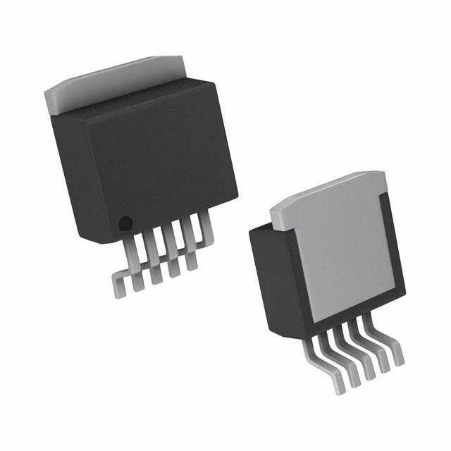
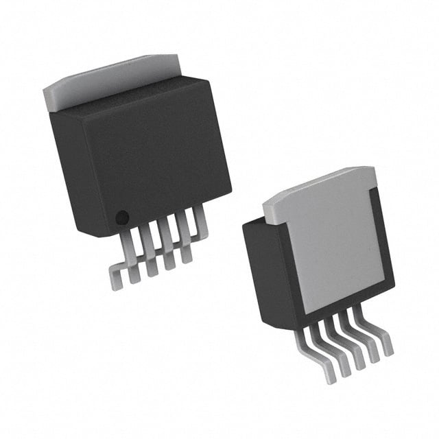
| 产品图片 |
|
| rohs | 符合RoHS无铅 / 符合限制有害物质指令(RoHS)规范要求 |
| 产品系列 | 电源管理 IC,低压差稳压器,Texas Instruments TPS75601KTTT- |
| 数据手册 | |
| 产品型号 | TPS75601KTTT |
| 产品种类 | 低压差稳压器 |
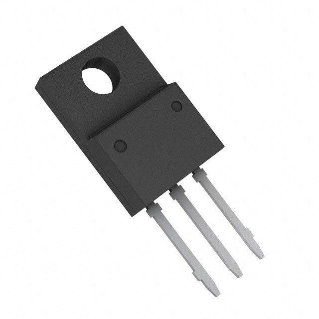
| 供应商器件封装 | DDPAK/TO-263-5 |
| 其它名称 | 296-15915-6 |
| 包装 | Digi-Reel® |
| 单位重量 | 1.456 g |
| 商标 | Texas Instruments |
| 安装类型 | 表面贴装 |
| 安装风格 | SMD/SMT |
| 封装 | Reel |
| 封装/外壳 | TO-263-6,D²Pak(5 引线+接片),TO-263BA |
| 封装/箱体 | TO-263-5 |
| 工作温度 | -40°C ~ 125°C |
| 工厂包装数量 | 50 |
| 最大工作温度 | + 125 C |
| 最大输入电压 | 5.5 V |
| 最小工作温度 | - 40 C |
| 最小输入电压 | + 2.8 V |
| 标准包装 | 1 |
| 电压-跌落(典型值) | 0.25V @ 5A |
| 电压-输入 | 2.8 V ~ 5.5 V |
| 电压-输出 | 1.22 V ~ 5 V |
| 电压调节准确度 | 2 % |
| 电流-输出 | 5A |
| 电流-限制(最小值) | 5.5A |
| 稳压器拓扑 | 正,可调式 |
| 稳压器数 | 1 |
| 系列 | TPS75601 |
| 线路调整率 | 0.04 % / V |
| 负载调节 | 0.35 % / V |
| 输入偏压电流—最大 | 0.125 mA |
| 输出电压 | 1.22 V to 5 V |
| 输出电流 | 5 A |
| 输出端数量 | 1 Output |
| 输出类型 | Adjustable |


- 商务部:美国ITC正式对集成电路等产品启动337调查
- 曝三星4nm工艺存在良率问题 高通将骁龙8 Gen1或转产台积电
- 太阳诱电将投资9.5亿元在常州建新厂生产MLCC 预计2023年完工
- 英特尔发布欧洲新工厂建设计划 深化IDM 2.0 战略
- 台积电先进制程称霸业界 有大客户加持明年业绩稳了
- 达到5530亿美元!SIA预计今年全球半导体销售额将创下新高
- 英特尔拟将自动驾驶子公司Mobileye上市 估值或超500亿美元
- 三星加码芯片和SET,合并消费电子和移动部门,撤换高东真等 CEO
- 三星电子宣布重大人事变动 还合并消费电子和移动部门
- 海关总署:前11个月进口集成电路产品价值2.52万亿元 增长14.8%


PDF Datasheet 数据手册内容提取
TPS75601, TPS75615 TPS75618, TPS75625 TPS75633 www.ti.com SLVS329C–JUNE2001–REVISEDMARCH2004 FAST-TRANSIENT RESPONSE 5-A LOW-DROPOUT VOLTAGE REGULATORS FEATURES DESCRIPTION • 5-ALow-DropoutVoltageRegulator The TPS756xx family of 5-A low dropout (LDO) • Availablein1.5-V,1.8-V,2.5-V,and3.3-V regulators contains four fixed voltage option regu- Fixed-OutputandAdjustableVersions lators and an adjustable voltage option regulator. These devices are capable of supplying 5 A of output • DropoutVoltageTypically250mVat5A current with a dropout of 250 mV (TPS75633). (TPS75633) Therefore, the device is capable of performing a • Low125µATypicalQuiescentCurrent 3.3-Vto2.5-Vconversion. • FastTransientResponse Quiescent current is 125 µA at full load and drops • 3%ToleranceOverSpecifiedConditionsfor down to less than 1 µA when the device is disabled. Fixed-OutputVersions The TPS756xx is designed to have fast transient • Availablein5-PinTO-220andTO-263Sur- responseforlargeloadcurrentchanges. face-MountPackages • ThermalShutdownProtection TO–220 (KC) PACKAGE TO–263 (KTT) PACKAGE (TOP VIEW) (TOP VIEW) EN 1 EN 1 IN 2 IN 2 GND 3 OUTPUT 4 GND 3 FB/NC 5 OUTPUT 4 FB/NC 5 TPS75633 DROPOUT VOLTAGE TPS75615 vs LOAD TRANSIENT RESPONSE 400 JUNCTION TEMPERATURE mV 150 VO = 1.5 V V 350 IVOO = = 5 3 A.3 V ge – 100 Co = 100 m F – m 300 olta 50 oltage 250 utput V 0 A opout V 125000 ge in O ––15000 ddti(cid:1)1.2(cid:1)5sA rrent – r n u D a C – O 100 Ch –150 5 ut VD – O utp 50 V O D – 0–40–25–10 5 20 35 50 65 80 95 110125 0 20 40 60 80 100 120140160180 2000 I O t – Time – m s TJ – Junction Temperature – °C Pleasebeawarethatanimportantnoticeconcerningavailability,standardwarranty,anduseincriticalapplicationsofTexas Instrumentssemiconductorproductsanddisclaimerstheretoappearsattheendofthisdatasheet. PowerPADisatrademarkofTexasInstruments. PRODUCTIONDATAinformationiscurrentasofpublicationdate. Copyright©2001–2004,TexasInstrumentsIncorporated Products conform to specifications per the terms of the Texas Instruments standard warranty. Production processing does not necessarilyincludetestingofallparameters.
TPS75601, TPS75615 TPS75618, TPS75625 TPS75633 www.ti.com SLVS329C–JUNE2001–REVISEDMARCH2004 Because the PMOS device behaves as a low-value resistor, the dropout voltage is very low (typically 250 mV at an output current of 5 A for the TPS75633) and is directly proportional to the output current. Additionally, since the PMOS pass element is a voltage-driven device, the quiescent current is very low and independent of output loading (typically 125 µA over the full range of output current). These two key specifications yield a significant improvementinoperatinglifeforbattery-poweredsystems. The device is enabled when EN (enable) is connected to a high voltage level (> 2 V). Applying a low voltage level(<0.7V)toENshutsdowntheregulator,reducingthequiescentcurrenttolessthan1µAatT =25(cid:176)C. J The TPS756xx is offered in 1.5-V, 1.8-V, 2.5-V, and 3.3-V fixed-voltage versions and in an adjustable version (programmable over the range of 1.22 V to 5 V). Output voltage tolerance is specified as a maximum of 3% over line, load, and temperature ranges. The TPS756xx family is available in a 5-pin TO-220 (KC) and TO-263 (KTT) packages. AVAILABLEOPTIONS T OUTPUTVOLTAGE(TYP) TO-220(KC) TO-263(KTT)(1) J 3.3V TPS75633KC TPS75633KTT 2.5V TPS75625KC TPS75625KTT -40(cid:176)C to+125(cid:176)C 1.8V TPS75618KC TPS75618KTT 1.5V TPS75615KC TPS75615KTT Adjustable1.22Vto5V TPS75601KC TPS75601KTT (1) TheTPS75601isprogrammableusinganexternalresistordivider(seeapplicationinformation).Add TforKTTdevicesin50-piecereel.AddRforKTTdevicesin500-piecereel. 2 5 VI IN NC 4 OUT VO 1 m F 1 EN Co(1) + 47 m F GND 3 (1) See application information section for capacitor selection details. Figure1.TypicalApplicationConfiguration(ForFixedOutputOptions) 2
TPS75601, TPS75615 TPS75618, TPS75625 TPS75633 www.ti.com SLVS329C–JUNE2001–REVISEDMARCH2004 FUNCTIONALBLOCKDIAGRAM—ADJUSTABLEVERSION VIN VOUT UVLO Current Sense SHUTDOWN ILIM R1 GND _ + FB EN UVLO R2 Thermal Shutdown External to the Device Vref = 1.22 V Bandgap VIN Reference FUNCTIONALBLOCKDIAGRAM—FIXEDVERSION VIN VOUT UVLO Current Sense SHUTDOWN ILIM R1 _ + GND UVLO EN R2 Thermal Shutdown Vref = 1.22 V Bandgap VIN Reference TERMINALFUNCTIONS(TPS756xx) TERMINAL I/O DESCRIPTION NAME NO. EN 1 I Enableinput FB/NC 5 I Feedbackinputvoltageforadjustabledevice/noconnectionforfixedoptions GND 3 Regulatorground IN 2 I Inputvoltage OUTPUT 4 O Regulatedoutputvoltage 3
TPS75601, TPS75615 TPS75618, TPS75625 TPS75633 www.ti.com SLVS329C–JUNE2001–REVISEDMARCH2004 DETAILED DESCRIPTION The TPS756xx family includes four fixed-output voltage regulators (1.5 V, 1.8 V, 2.5 V, and 3.3 V), and an adjustableregulator,theTPS75601(adjustablefrom1.22Vto5V).Thebandgapvoltageistypically1.22V. Pin Functions Enable(EN) The EN terminal is an input which enables or shuts down the device. If EN is a low voltage level (< 0.7 V), the device will be in shutdown or sleep mode. When EN goes to a high voltage level (> 2 V), the device will be enabled. Feedback(FB) FB is an input terminal used for the adjustable-output option and must be connected to the output terminal either directly, in order to generate the minimum output voltage of 1.22 V, or through an external feedback resistor divider for other output voltages. The FB connection should be as short as possible. It is essential to route it in such a way to minimize/avoid noise pickup. Adding RC networks between FB terminal and V to filter noise is O notrecommendedbecauseitmaycausetheregulatortooscillate. InputVoltage(IN) TheV terminalisaninputtotheregulator. IN OutputVoltage(OUTPUT) TheV terminalisanoutputfromtheregulator. OUTPUT ABSOLUTE MAXIMUM RATINGS overoperatingjunctiontemperaturerange(unlessotherwisenoted)(1)(2) UNIT Inputvoltagerange,V -0.3Vto6V I VoltagerangeatEN -0.3Vto6V Peakoutputcurrent Internallylimited Continuoustotalpowerdissipation SeeDissipationRatingTables Outputvoltage,V (OUTPUT,FB) 5.5V O Operatingjunctiontemperaturerange,T -40(cid:176)C to150(cid:176)C J Storagetemperaturerange,T -65(cid:176)C to150(cid:176)C stg ESDrating,HBM 2kV ESDrating,CDM 500V (1) Stressesbeyondthoselistedunder,,absolutemaximumratings”maycausepermanentdamagetothedevice.Thesearestressratings only,andfunctionaloperationofthedeviceattheseoranyotherconditionsbeyondthoseindicatedunder,,recommendedoperating conditions”isnotimplied.Exposuretoabsolute-maximum-ratedconditionsforextendedperiodsmayaffectdevicereliability. (2) Allvoltagevaluesarewithrespecttonetworkterminalground. DISSIPATION RATING TABLE package RQJC ((cid:176)C/W) RQJA ((cid:176)C/W) (1) TO-220 2 58.7(2) TO-263 2 38.7(3) (1) Forbothpackages,theRQJA valueswerecomputedusingJEDEChighKboard(2S2P)with1ounceinternalcopperplaneandground plane.Therewasnoairflowacrossthepackages. (2) RQJA wascomputedassumingavertical,freestandingTO-220packagewithpinssolderedtotheboard.Thereisnoheatsinkattached tothepackage. (3) RQJA wascomputedassumingahorizontallymountedTO-263packagewithpinssolderedtotheboard.Thereisnocopperpad underneaththepackage. 4
TPS75601, TPS75615 TPS75618, TPS75625 TPS75633 www.ti.com SLVS329C–JUNE2001–REVISEDMARCH2004 RECOMMENDED OPERATING CONDITIONS MIN MAX UNIT Inputvoltage,V(1) 2.8 5.5 V I Outputvoltagerange,V 1.22 5 V O Outputcurrent,I 0 5 A O Operatingvirtualjunctiontemperature,T -40 125 (cid:176)C J (1) Tocalculatetheminimuminputvoltageforyourmaximumoutputcurrent,usethefollowingequation:V =V +V . I(min) O(max) DO(maxload) ELECTRICAL CHARACTERISTICS overrecommendedoperatingjunctiontemperaturerange(T =-40(cid:176)C to125(cid:176)C), V=V (typ)+1V,I =1mA,EN=V, J I O O I C =100µF(unlessotherwisenoted) o PARAMETER TESTCONDITIONS MIN TYP MAX UNIT 1.22V£ V £ 5.5V,T =25(cid:176)C V O J O Adjustablevoltage 1.22V£ V £ 5.5V 0.97V 1.03V V O O O 1.22V£ V £ 5.5V,T =0to125(cid:176)C (2) 0.97V 1.03V O J O O T =25(cid:176)C, 2.8V<V <5.5V 1.5 J I 1.5VOutput V 2.8V£ V£ 5.5V 1.455 1.545 I Outputvoltage(1) T =25(cid:176)C, 2.8V<V <5.5V 1.8 J I 1.8VOutput V 2.8V£ V£ 5.5V 1.746 1.854 I T =25(cid:176)C, 3.5V<V <5.5V 2.5 J I 2.5VOutput V 3.5V£ V£ 5.5V 2.425 2.575 I T =25(cid:176)C, 4.3V<V <5.5V 3.3 J I 3.3VOutput V 4.3V£ V£ 5.5V 3.201 3.399 I T =25(cid:176)C 125 Quiescentcurrent(GNDcurrent) (1), (3) J µA 200 V +1V£ V£ 5.5V,T =25(cid:176)C 0.04 Outputvoltagelineregulation(DV /V )(3) O I J %/V O O V +1V£ V <5.5V 0.1 O I Loadregulation(1) 0.35 %/V Outputnoisevoltage TPS75615 BW=300Hzto50kHz,T =25(cid:176)C, V =2.8V 35 µVrms J I Outputcurrentlimit V =0V 5.5 10 14 A O Thermalshutdownjunctiontemperature 150 (cid:176)C EN=0 T =25(cid:176)C 0.1 µA J Standbycurrent EN=0 10 µA FBinputcurrent TPS75601 FB=1.5V -1 1 µA Powersupplyripple TPS75615 f=100Hz,T=25(cid:176)C, V =2.8V,I =5A 60 dB rejection J I O EN=V -1 1 µA I Inputcurrent(EN) EN=0V -1 0 1 µA HighlevelENinputvoltage 2 V LowlevelENinputvoltage 0.7 V (1) I =1mAto5A O (2) Theadjustableoptionoperateswitha2%toleranceoverT =0to125(cid:176)C. J (3) IfV <2.5VthenV =2.8V,V =5.5V: O Imin Imax Line regulator (mV)(cid:3)(%V)(cid:1)VO(cid:4)VIm1ax00(cid:2)2.8V(cid:5)(cid:1)1000 IfV ‡ 2.5VthenV =V +1V,V =5.5V: O Imin O Imax Line regulator (mV)(cid:4)(%V)(cid:1)VO(cid:5)VImax(cid:3)10(cid:5)0VO(cid:2)1V(cid:6)(cid:6)(cid:1)1000 5
TPS75601, TPS75615 TPS75618, TPS75625 TPS75633 www.ti.com SLVS329C–JUNE2001–REVISEDMARCH2004 ELECTRICAL CHARACTERISTICS (continued) overrecommendedoperatingjunctiontemperaturerange(T =-40(cid:176)C to125(cid:176)C), V=V (typ)+1V,I =1mA,EN=V, J I O O I C =100µF(unlessotherwisenoted) o PARAMETER TESTCONDITIONS MIN TYP MAX UNIT I =5A,V =3.2V,T =25(cid:176)C 250 Dropoutvoltage,(3.3Voutput) (4) O I J mV V I =5A,V =3.2V 500 O O I Dischargetransistorcurrent V =1.5V,T =25(cid:176)C 10 25 mA O J UVLO T =25(cid:176)C, V rising 2.2 2.75 V J I V I UVLOhysteresis T =25(cid:176)C, V falling 100 mV J I (4) IfV <2.5VthenV =2.8V,V =5.5V: O Imin Imax Line regulator (mV)(cid:3)(%V)(cid:1)VO(cid:4)VIm1ax00(cid:2)2.8V(cid:5)(cid:1)1000 IfV ‡ 2.5VthenV =V +1V,V =5.5V: O Imin O Imax Line regulator (mV)(cid:4)(%V)(cid:1)VO(cid:5)VImax(cid:3)10(cid:5)0VO(cid:2)1V(cid:6)(cid:6)(cid:1)1000 TYPICAL CHARACTERISTICS Table of Graphs FIGURE vsOutputcurrent 2,3 V Outputvoltage O vsJunctiontemperature 4,5 Groundcurrent vsJunctiontemperature 6 Powersupplyripplerejection vsFrequency 7 Outputspectralnoisedensity vsFrequency 8 z Outputimpedance vsFrequency 9 o vsInputvoltage 10 V Dropoutvoltage DO vsJunctiontemperature 11 V Minimumrequiredinputvoltage vsOutputvoltage 12 I Linetransientresponse 13,15 Loadtransientresponse 14,16 V Outputvoltageandenablevoltage vsTime(start-up) 17 O Equivalentseriesresistance vsOutputcurrent 19,20 6
TPS75601, TPS75615 TPS75618, TPS75625 TPS75633 www.ti.com SLVS329C–JUNE2001–REVISEDMARCH2004 TPS75633 TPS75615 OUTPUTVOLTAGE OUTPUTVOLTAGE vs vs OUTPUTCURRENT OUTPUTCURRENT 3.345 1.545 VI = 4.3 V VI = 2.8 V TJ = 25°C TJ = 25°C 3.330 1.530 V V − 3.315 − 1.515 e e g g a a olt olt V 3.3 V 1.5 ut ut p p ut ut O O − 3.285 − 1.485 O O V V 3.270 1.470 3.255 1.455 0 1 2 3 4 5 0 1 2 3 4 5 IO − Output Current − A IO − Output Current − A Figure2. Figure3. TPS75633 TPS75615 OUTPUTVOLTAGE OUTPUTVOLTAGE vs vs JUNCTIONTEMPERATURE JUNCTIONTEMPERATURE 3.345 1.545 VI = 4.3 V VI = 2.8 V 3.33 1.530 V V − 3.315 − 1.515 e e g g a a olt olt V 3.3 V 1.5 ut ut p p ut ut O O − 3.285 − 1.485 O O V V 3.270 1.470 3.255 1.455 −40 −25 10 5 20 35 50 65 80 95 110125 −40−25 −10 5 20 35 50 65 80 95 110 125 TJ − Junction Temperature − °C TJ − Junction Temperature − °C Figure4. Figure5. 7
TPS75601, TPS75615 TPS75618, TPS75625 TPS75633 www.ti.com SLVS329C–JUNE2001–REVISEDMARCH2004 TYPICAL CHARACTERISTICS (continued) TPS756xx TPS75633 GROUNDCURRENT POWERSUPPLYRIPPLEREJECTION vs vs JUNCTIONTEMPERATURE FREQUENCY 150 90 VI = 5 V B VI = 4.3 V IO = 5 A n − d 80 CTJo == 2150°0C m F o 70 ecti IO = 1 mA A 125 Rej 60 mnt − pple 50 urre y Ri 40 C pl und Sup 30 ro 100 er IO = 5 A G w 20 o P R − 10 R PS 0 75 −40 −25 −10 5 20 35 50 65 80 95 110 125 10 100 1k 10k 100k 1M 10M TJ − Junction Temperature − °C f − Frequency − Hz Figure6. Figure7. TPS75633 TPS75633 OUTPUTSPECTRALNOISEDENSITY OUTPUTIMPEDANCE vs vs FREQUENCY FREQUENCY 2.5 100 mV/Hz− 2 VVCTJIOo = === 4 213.530.3° 0CV Vm F 10 VCTJIo = == 4 21.530° 0CV m F sity IO = 5 A We − n c e n D 1.5 a e ed 1 IO = 1 mA s p oi m ctral N 1 IO = 1 mA utput I 0.1 e O Sp − ut zo p 0.5 ut 0.01 IO = 5 A O 0 0.001 1100 100 1k 10k 100k 10 100 1k 10k 100k 1M 10M f − Frequency − Hz f − Frequency − Hz Figure8. Figure9. 8
TPS75601, TPS75615 TPS75618, TPS75625 TPS75633 www.ti.com SLVS329C–JUNE2001–REVISEDMARCH2004 TYPICAL CHARACTERISTICS (continued) TPS75601 TPS75633 DROPOUTVOLTAGE DROPOUTVOLTAGE vs vs INPUTVOLTAGE JUNCTIONTEMPERATURE 450 400 IO = 5 A IO = 5 A 400 350 VO = 3.3 V mV 350 TJ = 125°C mV 300 e − 300 ge − ut Voltag 250 TTJ J= = − 2450°°CC out Volta 220500 po 200 op − Dro 150 − Dr 150 O O VD VD 100 100 50 50 0 0 2.5 3 3.5 4 4.5 5 −40 −25 −10 5 20 35 50 65 80 95 110 125 VI − Input Voltage − V TJ − Junction Temperature − °C Figure10. Figure11. MINIMUMREQUIREDINPUTVOLTAGE vs TPS75615 OUTPUTVOLTAGE LINETRANSIENTRESPONSE 4 nput Voltage − V IO = 5 A TJ = −4T0TJ° J=C = 2 152°C5°C V− Change inOutput Voltage − mV −55000 VICOOo = == 5 11A0.50 Vm F d I D O e 3 −100 uir Req 2.8 − V m ge u a nim Volt 3.8 Mi ut − p VI − In 2.8 VI 2 1.5 1.75 2 2.25 2.5 2.75 3 3.25 3.5 0 50 100 150 200 250 300 350 400 450 500 VO − Output Voltage − V t − Time − m s Figure12. Figure13. 9
TPS75601, TPS75615 TPS75618, TPS75625 TPS75633 www.ti.com SLVS329C–JUNE2001–REVISEDMARCH2004 TYPICAL CHARACTERISTICS (continued) TPS75615 TPS75633 LOADTRANSIENTRESPONSE LINETRANSIENTRESPONSE V 150 V m m ge − 100 VCOo == 110.50 Vm F ge − VIOO = = 5 3 A.3 V olta olta 50 Co = 100 m F ut V 50 ut V 0 p p Out 0 Out n n −50 e i e i g −50 g n n a a−100 h h − CVO−100 ddti(cid:1)1.2(cid:1)5sA ent − A − CVO ge − V D−150 5 Curr D 5.3Volta ut ut 0 p p Out 4.3− In 0 20 40 60 80 100 120 140 160 180 200 I − O VI t − Time − m s 0 50 100 150 200 250 300 350 400 450 500 t − Time − m s Figure14. Figure15. TPS75633 OUTPUTVOLTAGEANDENABLEVOLTAGE TPS75633 vs LOADTRANSIENTRESPONSE TIME(START-UP) V ge − m VCOo == 31 0.30 Vm F ge − V 3.3 VIOI == 140.3 m VA olta olta TJ = 25°C V V ut 200 ut p p ut ut O 100 O n − e i O ng 0 V 0 a A − ChO−100 ddti(cid:1)1.2(cid:1)5sA ent − − V 4.3 V urr ge D 5 ut C olta 0 p V ut e 0 O bl I − O Ena 0 20 40 60 80 100 120 140 160 180 200 0 0.2 0.4 0.6 0.8 1 t − Time − m s t − Time (Start-Up) − ms Figure16. Figure17. 10
TPS75601, TPS75615 TPS75618, TPS75625 TPS75633 www.ti.com SLVS329C–JUNE2001–REVISEDMARCH2004 TYPICAL CHARACTERISTICS (continued) To Load VI IN OUT + Co RL EN GND ESR Figure18.TestCircuitforTypicalRegionsofStability(Figures19and20)(FixedOutputOptions) TYPICALREGIONOFSTABILITY(A) TYPICALREGIONOFSTABILITY(A) EQUIVALENTSERIESRESISTANCE EQUIVALENTSERIESRESISTANCE vs vs OUTPUTCURRENT OUTPUTCURRENT 10 10 Co = 680 m F Co = 47 m F Wce − TJ = 25°C We − TJ = 25°C n c a n Resist 1 esista 1 es Region of Stability s R Region of Stability Seri erie ent nt S val ale 0.2 qui 0.1 uiv E q SR − R − E Region of Instability E S E 0.015 Region of Instability 0.01 0.01 0 1 2 3 4 5 0 1 2 3 4 5 IO − Output Current − A IO − Output Current − A Figure19. Figure20. A.Equivalentseriesresistance(ESR)referstothetotalseriesresistance,includingtheESRofthecapacitor,any seriesresistanceaddedexternally,andPWBtraceresistancetoC . O 11
TPS75601, TPS75615 TPS75618, TPS75625 TPS75633 www.ti.com SLVS329C–JUNE2001–REVISEDMARCH2004 THERMAL INFORMATION The amount of heat that an LDO linear regulator generates is directly proportional to the amount of power it dissipates during operation. All integrated circuits have a maximum allowable junction temperature (T max) J above which normal operation is not assured. A system designer must design the operating environment so that the operating junction temperature (T ) does not exceed the maximum junction temperature (T max). The two J J main environmental variables that a designer can use to improve thermal performance are air flow and external heatsinks. The purpose of this information is to aid the designer in determining the proper operating environment foralinearregulatorthatisoperatingataspecificpowerlevel. Ingeneral,themaximumexpectedpower(P )consumedbyalinearregulatoriscomputedas: D(max) (cid:5) (cid:6) PDmax(cid:4) VI(avg)(cid:3)VO(avg) (cid:1)IO(avg) (cid:2) VI(avg)xI(Q) (1) Where: • V istheaverageinputvoltage. I(avg) • V istheaverageoutputvoltage. O(avg) • I istheaverageoutputcurrent. O(avg) • I isthequiescentcurrent. (Q) For most TI LDO regulators, the quiescent current is insignificant compared to the average output current; therefore, the term V x I can be neglected. The operating junction temperature is computed by adding the I(avg) (Q) ambient temperature (T ) and the increase in temperature due to the regulator's power dissipation. The A temperature rise is computed by multiplying the maximum expected power dissipation by the sum of the thermal resistances between the junction and the case (RQJC ), the case to heatsink (RQCS ), and the heatsink to ambient (RQSA ). Thermal resistances are measures of how effectively an object dissipates heat. Typically, the larger the device,themoresurfaceareaavailableforpowerdissipationandthelowertheobject'sthermalresistance. Figure 21 illustrates these thermal resistances for (a) a TO-220 package attached to a heatsink, and (b) a TO-263packagemountedonaJEDECHigh-Kboard. C B A TJ A Rq JC A B B TC Rq CS C Rq SA C TO–263 Package TA (b) TO–220 Package (a) Figure21.ThermalResistances 12
TPS75601, TPS75615 TPS75618, TPS75625 TPS75633 www.ti.com SLVS329C–JUNE2001–REVISEDMARCH2004 THERMAL INFORMATION (continued) Equation2summarizesthecomputation: TJ (cid:2) TA(cid:1)PDmaxx(cid:3)Rq JC (cid:1) Rq CS (cid:1) Rq SA(cid:4) (2) The RQJC is specific to each regulator as determined by its package, lead frame, and die size provided in the regulator's data sheet. The RQSA is a function of the type and size of heatsink. For example, black body radiator type heatsinks, like the one attached to the TO-220 package in Figure 21(a), can have RQCS values ranging from 5(cid:176)C/W forverylargeheatsinksto50(cid:176)C/W forverysmallheatsinks.TheRQCS isafunctionofhowthepackageis attached to the heatsink. For example, if a thermal compound is used to attach a heatsink to a TO-220 package, RQCS of1(cid:176)C/W isreasonable. Even if no external black body radiator type heatsink is attached to the package, the board on which the regulator is mounted will provide some heatsinking through the pin solder connections. Some packages, like the TO-263 and TI's TSSOP PowerPAD™ packages, use a copper plane underneath the package or the circuit board's ground plane for additional heatsinking to improve their thermal performance. Computer aided thermal modeling can be used to compute very accurate approximations of an integrated circuit's thermal performance in different operating environments (e.g., different types of circuit boards, different types and sizes of heatsinks, different air flows, etc.). Using these models, the three thermal resistances can be combined into one thermal resistance between junction and ambient (RQJA ). This RQJA is valid only for the specific operating environment usedinthecomputermodel. Equation2simplifiesintoEquation3: T (cid:2) T (cid:1)P maxx R J A D q JA (3) RearrangingEquation3givesEquation4: T –T R (cid:1) J A q JA P max D (4) Using Equation 3 and the computer model generated curves shown in Figure 22 and Figure 25, a designer can quickly compute the required heatsink thermal resistance/board area for a given ambient temperature, power dissipation,andoperatingenvironment. TO-220 Power Dissipation The TO-220 package provides an effective means of managing power dissipation in through-hole applications. The TO-220 package dimensions are provided in the Mechanical Data section at the end of the data sheet. A heatsinkcanbeusedwiththeTO-220packagetoeffectivelylowerthejunction-to-ambientthermalresistance. To illustrate, the TPS75625 in a TO-220 package was chosen. For this example, the average input voltage is 3.3 V, the average output voltage is 2.5 V, the average output current is 3 A, the ambient temperature 55(cid:176)C, the air flow is 150 LFM, and the operating environment is the same as documented below. Neglecting the quiescent current,themaximumaveragepoweris: P max (cid:1) (3.3–2.5)Vx3A (cid:1) 2.4W D (5) SubstitutingT maxforT intoEquation4givesEquation6: J J Rq JAmax (cid:1) (125–55)°C(cid:2)2.4W (cid:1) 29°C(cid:2)W (6) From Figure 22, RQJA vs Heatsink Thermal Resistance, a heatsink with RQSA = 22(cid:176)C/W is required to dissipate 2.4 W. The model operating environment used in the computer model to construct Figure 22 consisted of a standard JEDEC High-K board (2S2P) with a 1 oz. internal copper plane and ground plane. Since the package pins were soldered to the board, 450 mm2 of the board was modeled as a heatsink. Figure 23 shows the side viewoftheoperatingenvironmentusedinthecomputermodel. 13
TPS75601, TPS75615 TPS75618, TPS75625 TPS75633 www.ti.com SLVS329C–JUNE2001–REVISEDMARCH2004 THERMAL INFORMATION (continued) THERMAL RESISTANCE vs HEATSINK THERMAL RESISTANCE 65 Natural Convection W 55 C/ ° – Air Flow = 150 LFM e 45 nc Air Flow = 250 LFM a st Air Flow = 500 LFM esi 35 R al m er 25 h T – A J 15 Rq No Heatsink 5 25 20 15 10 5 0 Rq SA – Heatsink Thermal Resistance – °C/W Figure22. 0.21 mm 0.21 mm 1 oz. Copper 1 oz. Copper Power Plane Ground Plane Figure23. From the data in Figure 22 and rearranging Equation 4, the maximum power dissipation for a different heatsink RQSA andaspecificambienttemperaturecanbecomputed(seeFigure24). 14
TPS75601, TPS75615 TPS75618, TPS75625 TPS75633 www.ti.com SLVS329C–JUNE2001–REVISEDMARCH2004 THERMAL INFORMATION (continued) POWER DISSIPATION LIMIT vs HEATSINK THERMAL RESISTANCE 10 TA = 55°C W Air Flow = 500 LFM – mit Air Flow = 250 LFM Li n atio Air Flow = 150 LFM p si s Di r e w o P – D P Natural Convection No Heatsink 1 20 10 0 Rq SA – Heatsink Thermal Resistance – °C/W Figure24. TO-263 Power Dissipation The TO-263 package provides an effective means of managing power dissipation in surface-mount applications. The TO-263 package dimensions are provided in the Mechanical Data section at the end of the data sheet. The addition of a copper plane directly underneath the TO-263 package enhances the thermal performance of the package. To illustrate, the TPS75625 in a TO-263 package was chosen. For this example, the average input voltage is 3.3 V, the average output voltage is 2.5 V, the average output current is 3 A, the ambient temperature 55(cid:176)C, the air flow is 150 LFM, and the operating environment is the same as documented below. Neglecting the quiescent current,themaximumaveragepoweris: P max (cid:1) (3.3–2.5)Vx3A (cid:1) 2.4W D (7) SubstitutingT maxforT intoEquation4givesEquation8: J J Rq JAmax (cid:1) (125–55)°C(cid:2)2.4W (cid:1) 29°C(cid:2)W (8) From Figure 25, RQJA vs Copper Heatsink Area, the ground plane needs to be 2 cm2 for the part to dissipate 2.4 W. The model operating environment used in the computer model to construct Figure 25 consisted of a standard JEDEC High-K board (2S2P) with a 1 oz. internal copper plane and ground plane. The package is soldered to a 2 oz. copper pad. The pad is tied through thermal vias to the 1 oz. ground plane. Figure 26 shows the side view oftheoperatingenvironmentusedinthecomputermodel. 15
TPS75601, TPS75615 TPS75618, TPS75625 TPS75633 www.ti.com SLVS329C–JUNE2001–REVISEDMARCH2004 THERMAL INFORMATION (continued) THERMAL RESISTANCE vs COPPER HEATSINK AREA 40 No Air Flow W C/ 35 ° – e 150 LFM c n a st 30 si Re 250 LFM al m er 25 h T – A J Rq 20 15 0 0.01 0.1 1 10 100 Copper Heatsink Area – cm2 Figure25. 2 oz. Copper Solder Pad With 25 Thermal Vias 1 oz. Copper Power Plane 1 oz. Copper Ground Plane Thermal Vias, 0.3 mm Diameter, 1.5 mm Pitch Figure26. From the data in Figure 25 and rearranging Equation 4, the maximum power dissipation for a different ground planeareaandaspecificambienttemperaturecanbecomputed(seeFigure27). 16
TPS75601, TPS75615 TPS75618, TPS75625 TPS75633 www.ti.com SLVS329C–JUNE2001–REVISEDMARCH2004 THERMAL INFORMATION (continued) MAXIMUM POWER DISSIPATION vs COPPER HEATSINK AREA 5 TA = 55°C W – n atio 4 250 LFM p si s Di er 150 LFM w 3 o P m u m xi No Air Flow a M 2 – D P 1 0 0.01 0.1 1 10 100 Copper Heatsink Area – cm2 Figure27. 17
TPS75601, TPS75615 TPS75618, TPS75625 TPS75633 www.ti.com SLVS329C–JUNE2001–REVISEDMARCH2004 APPLICATION INFORMATION The output voltage of the TPS75601 adjustable regulator is programmed using an external resistor divider as showninFigure28.Theoutputvoltageiscalculatedusing: V (V (cid:2)2.8V) Line regulator (mV)(cid:3)(%V)(cid:1) O Imax (cid:1)1000 100 (9) Resistors R1 and R2 should be chosen for approximately 40-µA divider current. Lower value resistors can be used but offer no inherent advantage and waste more power. Higher values should be avoided as leakage currents at FB increase the output voltage error. The recommended design procedure is to choose R2 = 30.1kW tosetthedividercurrentat40µAandthencalculateR1using: (cid:4)V (cid:5) O R1(cid:3) (cid:2)1 (cid:1)R2 V ref (10) TPS75601 OUTPUT VOLTAGE PROGRAMMING GUIDE VI IN 1 m F OUTPUT R1 R2 UNIT VOLTAGE ≥ 2 V EN OUT VO 2.5 V 31.6 30.1 kW ≤ 0.7 V R1 Co 3.3 V 51 30.1 kW FB 3.6 V 58.3 30.1 kW GND R2 Figure28.TPS75601AdjustableLDORegulatorProgramming Regulator Protection The TPS756xx PMOS-pass transistor has a built-in back diode that conducts reverse currents when the input voltage drops below the output voltage (e.g., during power down). Current is conducted from the output to the input and is not internally limited. When extended reverse voltage is anticipated, external limiting may be appropriate. The TPS756xx also features internal current limiting and thermal protection. During normal operation, the TPS756xx limits output current to approximately 10 A. When current limiting engages, the output voltage scales back linearly until the overcurrent condition ends. While current limiting is designed to prevent gross device failure,careshouldbetakennottoexceed the power dissipation ratings of the package. If the temperature of the device exceeds 150(cid:176)C (typ), thermal-protection circuitry shuts it down. Once the device has cooled below 130(cid:176)C (typ),regulatoroperationresumes. Input Capacitor For a typical application, a ceramic input bypass capacitor (0.22 µF-1 µF) is recommended to ensure device stability.Thiscapacitorshouldbeas close as possible to the input pin. Due to the impedance of the input supply, large transient currents will cause the input voltage to droop. If this droop causes the input voltage to drop below the UVLO threshold, the device will turn off. Therefore, it is recommended that a larger capacitor be placed in parallel with the ceramic bypass capacitor at the regulator's input. The size of this capacitor depends on the output current, response time of the main power supply, and the main power supply's distance to the regulator. At a minimum, the capacitor should be sized to ensure that the input voltage does not drop below the minimum UVLOthresholdvoltageduringnormaloperatingconditions. 18
TPS75601, TPS75615 TPS75618, TPS75625 TPS75633 www.ti.com SLVS329C–JUNE2001–REVISEDMARCH2004 APPLICATION INFORMATION (continued) Output Capacitor As with most LDO regulators, the TPS756xx requires an output capacitor connected between OUT and GND to stabilize the internal control loop. The minimum recommended capacitance value is 47 µF with an ESR (equivalent series resistance) of at least 200 mW. As shown in Figure 29, most capacitor and ESR combinations withaproductof47e-6x0.2=9.4e-6orlargerwillbestable, provided the capacitor value is at least 47 µF. Solid tantalum electrolytic and aluminum electrolytic capacitors are all suitable, provided they meet the requirements describedinthissection.Largercapacitorsprovideawiderrangeofstabilityandbetterloadtransientresponse. This information along with the ESR graphs, Figure 19, Figure 20, and Figure 29, is included to assist in selection of suitable capacitance for the user's application. When necessary to achieve low height requirements along with high output current and/or high load capacitance, several higher ESR capacitors can be used in paralleltomeettheseguidelines. OUTPUT CAPACITANCE vs EQUIVALENT SERIES RESISTANCE 1000 Region of Stability F m– e c n a cit ESR min x Co = Constant pa 100 a C ut p ut 47 O Region of Instability Y = ESRmin x Co 10 0.01 0.1 0.2 ESR – Equivalent Series Resistance – W Figure29. 19
PACKAGE OPTION ADDENDUM www.ti.com 6-Feb-2020 PACKAGING INFORMATION Orderable Device Status Package Type Package Pins Package Eco Plan Lead/Ball Finish MSL Peak Temp Op Temp (°C) Device Marking Samples (1) Drawing Qty (2) (6) (3) (4/5) TPS75601KC ACTIVE TO-220 KC 5 50 Green (RoHS Call TI | SN N / A for Pkg Type -40 to 85 75601 & no Sb/Br) TPS75601KTTR ACTIVE DDPAK/ KTT 5 500 Green (RoHS Call TI | SN Level-2-260C-1 YEAR -40 to 85 75601 TO-263 & no Sb/Br) TPS75601KTTRG3 ACTIVE DDPAK/ KTT 5 500 Green (RoHS SN Level-2-260C-1 YEAR -40 to 85 75601 TO-263 & no Sb/Br) TPS75615KC ACTIVE TO-220 KC 5 50 Green (RoHS Call TI | SN N / A for Pkg Type -40 to 85 75615 & no Sb/Br) TPS75615KCG3 ACTIVE TO-220 KC 5 50 Green (RoHS SN N / A for Pkg Type -40 to 85 75615 & no Sb/Br) TPS75615KTTT ACTIVE DDPAK/ KTT 5 50 Green (RoHS Call TI | SN Level-2-260C-1 YEAR 75615 TO-263 & no Sb/Br) TPS75615KTTTG3 ACTIVE DDPAK/ KTT 5 50 Green (RoHS SN Level-2-260C-1 YEAR 75615 TO-263 & no Sb/Br) TPS75618KC ACTIVE TO-220 KC 5 50 Green (RoHS Call TI | SN N / A for Pkg Type -40 to 85 75618 & no Sb/Br) TPS75618KTTT ACTIVE DDPAK/ KTT 5 50 Green (RoHS Call TI | SN Level-2-260C-1 YEAR 75618 TO-263 & no Sb/Br) TPS75618KTTTG3 ACTIVE DDPAK/ KTT 5 50 Green (RoHS SN Level-2-260C-1 YEAR 75618 TO-263 & no Sb/Br) TPS75625KC ACTIVE TO-220 KC 5 50 Green (RoHS Call TI | SN N / A for Pkg Type -40 to 85 75625 & no Sb/Br) TPS75625KTTR ACTIVE DDPAK/ KTT 5 500 Green (RoHS Call TI | SN Level-2-260C-1 YEAR -40 to 85 75625 TO-263 & no Sb/Br) TPS75633KC ACTIVE TO-220 KC 5 50 Green (RoHS Call TI | SN N / A for Pkg Type -40 to 85 75633 & no Sb/Br) TPS75633KCG3 ACTIVE TO-220 KC 5 50 Green (RoHS SN N / A for Pkg Type -40 to 85 75633 & no Sb/Br) TPS75633KTTT ACTIVE DDPAK/ KTT 5 50 Green (RoHS Call TI | SN Level-2-260C-1 YEAR 75633 TO-263 & no Sb/Br) TPS75633KTTTG3 ACTIVE DDPAK/ KTT 5 50 Green (RoHS SN Level-2-260C-1 YEAR 75633 TO-263 & no Sb/Br) (1) The marketing status values are defined as follows: ACTIVE: Product device recommended for new designs. Addendum-Page 1
PACKAGE OPTION ADDENDUM www.ti.com 6-Feb-2020 LIFEBUY: TI has announced that the device will be discontinued, and a lifetime-buy period is in effect. NRND: Not recommended for new designs. Device is in production to support existing customers, but TI does not recommend using this part in a new design. PREVIEW: Device has been announced but is not in production. Samples may or may not be available. OBSOLETE: TI has discontinued the production of the device. (2) RoHS: TI defines "RoHS" to mean semiconductor products that are compliant with the current EU RoHS requirements for all 10 RoHS substances, including the requirement that RoHS substance do not exceed 0.1% by weight in homogeneous materials. Where designed to be soldered at high temperatures, "RoHS" products are suitable for use in specified lead-free processes. TI may reference these types of products as "Pb-Free". RoHS Exempt: TI defines "RoHS Exempt" to mean products that contain lead but are compliant with EU RoHS pursuant to a specific EU RoHS exemption. Green: TI defines "Green" to mean the content of Chlorine (Cl) and Bromine (Br) based flame retardants meet JS709B low halogen requirements of <=1000ppm threshold. Antimony trioxide based flame retardants must also meet the <=1000ppm threshold requirement. (3) MSL, Peak Temp. - The Moisture Sensitivity Level rating according to the JEDEC industry standard classifications, and peak solder temperature. (4) There may be additional marking, which relates to the logo, the lot trace code information, or the environmental category on the device. (5) Multiple Device Markings will be inside parentheses. Only one Device Marking contained in parentheses and separated by a "~" will appear on a device. If a line is indented then it is a continuation of the previous line and the two combined represent the entire Device Marking for that device. (6) Lead/Ball Finish - Orderable Devices may have multiple material finish options. Finish options are separated by a vertical ruled line. Lead/Ball Finish values may wrap to two lines if the finish value exceeds the maximum column width. Important Information and Disclaimer:The information provided on this page represents TI's knowledge and belief as of the date that it is provided. TI bases its knowledge and belief on information provided by third parties, and makes no representation or warranty as to the accuracy of such information. Efforts are underway to better integrate information from third parties. TI has taken and continues to take reasonable steps to provide representative and accurate information but may not have conducted destructive testing or chemical analysis on incoming materials and chemicals. TI and TI suppliers consider certain information to be proprietary, and thus CAS numbers and other limited information may not be available for release. In no event shall TI's liability arising out of such information exceed the total purchase price of the TI part(s) at issue in this document sold by TI to Customer on an annual basis. Addendum-Page 2
PACKAGE MATERIALS INFORMATION www.ti.com 19-May-2020 TAPE AND REEL INFORMATION *Alldimensionsarenominal Device Package Package Pins SPQ Reel Reel A0 B0 K0 P1 W Pin1 Type Drawing Diameter Width (mm) (mm) (mm) (mm) (mm) Quadrant (mm) W1(mm) TPS75601KTTR DDPAK/ KTT 5 500 330.0 24.4 10.6 15.6 4.9 16.0 24.0 Q2 TO-263 TPS75625KTTR DDPAK/ KTT 5 500 330.0 24.4 10.6 15.6 4.9 16.0 24.0 Q2 TO-263 PackMaterials-Page1
PACKAGE MATERIALS INFORMATION www.ti.com 19-May-2020 *Alldimensionsarenominal Device PackageType PackageDrawing Pins SPQ Length(mm) Width(mm) Height(mm) TPS75601KTTR DDPAK/TO-263 KTT 5 500 367.0 367.0 45.0 TPS75625KTTR DDPAK/TO-263 KTT 5 500 367.0 367.0 45.0 PackMaterials-Page2
PACKAGE OUTLINE KC0005A TO-220 - 16.51 mm max height SCALE 0.850 TO-220 4.83 B 4.06 10.67 1.40 AAAAA 8.89 3.05 9.65 1.14 6.86 2.54 6.86 (6.275) 5.69 3.71-3.96 OPTIONAL 12.88 CHAMFER 10.08 16.51 2X (R1) MAX OPTIONAL 9.25 7.67 (4.25) C PIN 1 ID (OPTIONAL) NOTE 3 14.73 12.29 1 5 0.61 1.02 5X 0.30 0.64 3.05 0.25 C A B 2.03 4X 1.7 6.8 1 5 4215009/A 01/2017 NOTES: 1. All controlling linear dimensions are in inches. Dimensions in brackets are in millimeters. Any dimension in brackets or parenthesis are for reference only. Dimensioning and tolerancing per ASME Y14.5M. 2. This drawing is subject to change without notice. 3. Shape may vary per different assembly sites. www.ti.com
EXAMPLE BOARD LAYOUT KC0005A TO-220 - 16.51 mm max height TO-220 4X (1.45) PKG 0.07 MAX METAL 0.07 MAX ALL AROUND (1.45) TYP ALL AROUND PKG (2) 4X (2) 1 5 (R0.05) TYP SOLDER MASK FULL R (1.7) TYP OPENING, TYP TYP 5X ( 1.2) (6.8) LAND PATTERN NON-SOLDER MASK DEFINED SCALE:12X 4215009/A 01/2017 www.ti.com
None
None
IMPORTANTNOTICEANDDISCLAIMER TI PROVIDES TECHNICAL AND RELIABILITY DATA (INCLUDING DATASHEETS), DESIGN RESOURCES (INCLUDING REFERENCE DESIGNS), APPLICATION OR OTHER DESIGN ADVICE, WEB TOOLS, SAFETY INFORMATION, AND OTHER RESOURCES “AS IS” AND WITH ALL FAULTS, AND DISCLAIMS ALL WARRANTIES, EXPRESS AND IMPLIED, INCLUDING WITHOUT LIMITATION ANY IMPLIED WARRANTIES OF MERCHANTABILITY, FITNESS FOR A PARTICULAR PURPOSE OR NON-INFRINGEMENT OF THIRD PARTY INTELLECTUAL PROPERTY RIGHTS. These resources are intended for skilled developers designing with TI products. You are solely responsible for (1) selecting the appropriate TI products for your application, (2) designing, validating and testing your application, and (3) ensuring your application meets applicable standards, and any other safety, security, or other requirements. These resources are subject to change without notice. TI grants you permission to use these resources only for development of an application that uses the TI products described in the resource. Other reproduction and display of these resources is prohibited. No license is granted to any other TI intellectual property right or to any third party intellectual property right. TI disclaims responsibility for, and you will fully indemnify TI and its representatives against, any claims, damages, costs, losses, and liabilities arising out of your use of these resources. TI’s products are provided subject to TI’s Terms of Sale (www.ti.com/legal/termsofsale.html) or other applicable terms available either on ti.com or provided in conjunction with such TI products. TI’s provision of these resources does not expand or otherwise alter TI’s applicable warranties or warranty disclaimers for TI products. Mailing Address: Texas Instruments, Post Office Box 655303, Dallas, Texas 75265 Copyright © 2020, Texas Instruments Incorporated