ICGOO在线商城 > LM3280TL-275/NOPB

 Datasheet下载
- 型号: LM3280TL-275/NOPB
- 制造商: Texas Instruments
- 库位|库存: xxxx|xxxx
- 要求:
| 数量阶梯 | 香港交货 | 国内含税 |
| +xxxx | $xxxx | ¥xxxx |
查看当月历史价格
查看今年历史价格
LM3280TL-275/NOPB产品简介:
ICGOO电子元器件商城为您提供LM3280TL-275/NOPB由Texas Instruments设计生产,在icgoo商城现货销售,并且可以通过原厂、代理商等渠道进行代购。 提供LM3280TL-275/NOPB价格参考以及Texas InstrumentsLM3280TL-275/NOPB封装/规格参数等产品信息。 你可以下载LM3280TL-275/NOPB参考资料、Datasheet数据手册功能说明书, 资料中有LM3280TL-275/NOPB详细功能的应用电路图电压和使用方法及教程。
| 参数 | 数值 |
| 产品目录 | 集成电路 (IC)半导体 |
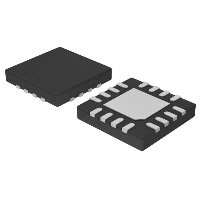
| 描述 | IC REG QD BUCK/LINEAR 16USMD稳压器—开关式稳压器 Adjustable Step-Down DC-DC Converter and 3 LDOs for RF Power Management 16-DSBGA -30 to 85 |
| 产品分类 | |
| 品牌 | Texas Instruments |
| 产品手册 | |
| 产品图片 |
|
| rohs | 符合RoHS无铅 / 符合限制有害物质指令(RoHS)规范要求 |
| 产品系列 | 电源管理 IC,稳压器—开关式稳压器,Texas Instruments LM3280TL-275/NOPB- |
| 数据手册 | |
| 产品型号 | LM3280TL-275/NOPB |
| 产品种类 | 稳压器—开关式稳压器 |
| 供应商器件封装 | 16-TuSMD |
| 其它名称 | LM3280TL-275/NOPBCT |
| 功能 | 任何功能 |
| 包装 | 剪切带 (CT) |
| 商标 | Texas Instruments |
| 安装类型 | 表面贴装 |
| 安装风格 | SMD/SMT |
| 封装 | Reel |
| 封装/外壳 | 16-WFBGA |
| 封装/箱体 | DSBGA-16 |
| 工作温度 | -30°C ~ 85°C |
| 工作温度范围 | - 30 C to + 85 C |
| 工厂包装数量 | 250 |
| 带LED驱动器 | 无 |
| 带定序器 | 无 |
| 带监控器 | 无 |
| 开关频率 | 2 MHz |
| 拓扑 | 降压(降压)(1),线性(LDO)(3) |
| 拓扑结构 | Buck |
| 最大工作温度 | + 85 C |
| 最大输入电压 | 5.5 V |
| 最小工作温度 | - 30 C |
| 最小输入电压 | 2.7 V |
| 标准包装 | 1 |
| 电压-电源 | 2.7 V ~ 5.5 V |
| 电压/电流-输出1 | 0.8 V ~ 3.6 V,300mA |
| 电压/电流-输出2 | 2.85V,20mA |
| 电压/电流-输出3 | 2.75V,20mA |
| 电源电压-最小 | 2.7 V |
| 类型 | Voltage Converter |
| 系列 | LM3280 |
| 输出数 | 4 |
| 输出电压 | 800 mV to 3.6 V |
| 输出电流 | 300 mA |
| 输出端数量 | 4 Output |
| 配用 | /product-detail/zh/LM3280TLEV/LM3280TLEV-ND/1640658 |
| 频率-开关 | 2MHz |


- 商务部:美国ITC正式对集成电路等产品启动337调查
- 曝三星4nm工艺存在良率问题 高通将骁龙8 Gen1或转产台积电
- 太阳诱电将投资9.5亿元在常州建新厂生产MLCC 预计2023年完工
- 英特尔发布欧洲新工厂建设计划 深化IDM 2.0 战略
- 台积电先进制程称霸业界 有大客户加持明年业绩稳了
- 达到5530亿美元!SIA预计今年全球半导体销售额将创下新高
- 英特尔拟将自动驾驶子公司Mobileye上市 估值或超500亿美元
- 三星加码芯片和SET,合并消费电子和移动部门,撤换高东真等 CEO
- 三星电子宣布重大人事变动 还合并消费电子和移动部门
- 海关总署:前11个月进口集成电路产品价值2.52万亿元 增长14.8%


PDF Datasheet 数据手册内容提取
LM3280 www.ti.com SNOSAU4B–OCTOBER2006–REVISEDFEBRUARY2013 LM3280 Adjustable Step-Down DC-DC Converter and 3 LDOs for RF Power Management CheckforSamples:LM3280 FEATURES DESCRIPTION 1 • 2MHz(typ.)PWMSwitchingFrequency The LM3280 is a multi-functional Power Management 2 Unit, optimized for low-power handheld applications • OperatesfromaSingleLi-IonCell(2.7Vto suchasCellularPhones. 5.5V) The LM3280 incorporates three low-dropout LDO • AdjustableOutputVoltage(0.8Vto3.6V)DC- voltage regulators and one step down PWM DC-DC DC converter with an internal Bypass FET. The step • High-EfficiencySynchronousBuckConverter down converter's output voltage can be set using an • 300mAMaximumLoadCapability(PWMMode) analog input (VCON) for optimizing efficiency of the RF PA at various power levels. The LDO operates a • 500mAMaximumLoadCapability(Bypass nominal output voltage of 2.85V and maximum load mode) current capability of 20mA for a reference voltage • PWM,ForcedandAutomaticBypassMode required by linear RF power amplifiers. The LM3280 • 3Low-DropoutandFastTransientResponse additionally features a separate enable pin for each LDOs output. • 16-pinDSBGAPackage TheLM3280isavailableina16-pinleadfreeDSBGA package. • CurrentOverloadProtection • ThermalOverloadProtection APPLICATIONS • CellularPhones • Hand-HeldRadios • BatteryPoweredRFDevices Typical Application VIN : C3 C1 2.7V to 5.5V 1 ØF 10 ØF L1 VOUT : VCON : SVIN PVIN BYPOUT 2.2 ØH 0.8V to 3.6V 0.267V to 1.200V SW VCON C2 VOUT = 3 x VCON FB 4.7 ØF DAC BYP PA VCC ON/OFF ENBUCK LM3280 LDO1 C5 VLDO1 : 2.85VVRE BAPNAD 1 ØPC ON/OFF ENLDO1 1 ØF VLDO2 :2.85V F PA LDO2 C6 VRE BAND2 ON/OFF ENLDO2 1 ØF F VLDO3 : 2.85V PA ON/OFF ENLDO3 SGND PGND LDO3 C7 VRE BAND3 1 ØF F Figure1. LM3280TypicalApplication 1 Pleasebeawarethatanimportantnoticeconcerningavailability,standardwarranty,anduseincriticalapplicationsof TexasInstrumentssemiconductorproductsanddisclaimerstheretoappearsattheendofthisdatasheet. Alltrademarksarethepropertyoftheirrespectiveowners. 2 PRODUCTIONDATAinformationiscurrentasofpublicationdate. Copyright©2006–2013,TexasInstrumentsIncorporated Products conform to specifications per the terms of the Texas Instruments standard warranty. Production processing does not necessarilyincludetestingofallparameters.
LM3280 SNOSAU4B–OCTOBER2006–REVISEDFEBRUARY2013 www.ti.com Connection Diagrams A LDO1 SVIN SGND BYPOUT B LDO2 FB ENBUCK PVIN C LDO3 ENLDO2 ENLDO1 SW D ENLDO3 VCON BYP PGND 1 2 3 4 Top View Figure2. 16–BumpDSBGAPackage,LargeBump SeePackageNumberYZR0016QQA PinDescriptions Pin# Name Description A1 LDO1 LDO1Output. B1 LDO2 LDO2Output. C1 LDO3 LDO3Output. D1 EN LDO3EnableInput.SetthisdigitalinputhightoturnonLDO3.(EN pinmustbealsosethigh.)For LDO3 BUCK turningLDO3off,setlow. A2 SVIN Analog,Signal,andLDOSupplyInput. B2 FB BuckConverterFeedbackAnalogInput.Connecttotheoutputattheoutputfiltercapacitor. C2 EN LDO2EnableInput.SetthisdigitalinputhightoturnonLDO2.(EN pinmustbealsosethigh.)For LDO2 BUCK turningLDO2off,setlow. D2 V BuckConverterVoltageControlAnalogInput.ThispincontrolsV inPWMmode.Set:V =3xV Do CON OUT OUT CON. notleavefloating. A3 SGND Analog,Signal,andLDOGround. B3 EN BuckConverterEnableInput.SetthisdigitalinputhighafterVin>2.7Vfornormaloperation.Forshutdown, BUCK setlow. C3 EN LDO1EnableInput.SetthisdigitalinputhightoturnonLDO1.(EN pinmustbealsosethigh.)For LDO1 BUCK turningLDO1off,setlow. D3 BYP ForcedBypassInput.UsethisdigitalinputtocommandoperationinBypassmode.SetBYPlow(<0.4V)for normaloperation. A4 BYPOUT BypassFETDrain.Connecttotheoutputcapacitor.Donotleavefloating. B4 PVIN BuckConverterPowerSupplyVoltageInputtotheinternalPFETswitchandBypassFET. C4 SW BuckConverterSwitchNodeconnectiontotheinternalPFETswitchandNFETsynchronousrectifier. ConnecttoaninductorwithasaturationcurrentratingthatexceedsthemaximumSwitchPeakCurrentLimit ofthePWMBuckConverter. D4 PGND BuckConverterPowerGround. Thesedeviceshavelimitedbuilt-inESDprotection.Theleadsshouldbeshortedtogetherorthedeviceplacedinconductivefoam duringstorageorhandlingtopreventelectrostaticdamagetotheMOSgates. 2 SubmitDocumentationFeedback Copyright©2006–2013,TexasInstrumentsIncorporated ProductFolderLinks:LM3280
LM3280 www.ti.com SNOSAU4B–OCTOBER2006–REVISEDFEBRUARY2013 Absolute Maximum Ratings(1)(2) SVIN,PVINtoSGND −0.2Vto+6.0V PGNDtoSGND −0.2Vto+0.2V ENs,FB,BYP,V (SGND−0.2V) CON to(SVIN+0.2V) w/6.0Vmax SW,BYPOUT (PGND−0.2V) to(PVIN+0.2V) w/6.0Vmax PVINtoSVIN −0.2Vto+0.2V ContinuousPowerDissipation (3) InternallyLimited JunctionTemperature(T ) +150°C J-MAX StorageTemperatureRange −65°Cto+150°C MaximumLeadTemperature (Soldering,10sec.) +260°C ESDRating (4) HumanBodyModel 2kV MachineModel 200V (1) AbsoluteMaximumRatingsindicatelimitsbeyondwhichdamagetothecomponentmayoccur.OperatingRatingsareconditionsunder whichoperationofthedeviceisguaranteed.OperatingRatingsdonotimplyguaranteedperformancelimits.Forguaranteed performancelimitsandassociatedtestconditions,seetheElectricalCharacteristicstables. (2) AllvoltagesarewithrespecttothepotentialattheGNDpins. (3) Internalthermalshutdowncircuitryprotectsthedevicefrompermanentdamage.ThermalshutdownengagesatT =150°C(typ.)and J disengagesatT =125°C(typ.). J (4) TheHumanbodymodelisa100pFcapacitordischargedthrougha1.5kΩresistorintoeachpin.(MIL-STD-8833015.7)Themachine modelisa200pFcapacitordischargeddirectlyintoeachpin.NationalSemiconductorrecommendsthatallintegratedcircuitsbe handledwithappropriateprecautions.FailuretoobserveproperESDhandlingtechniquescanresultindamage. Operating Ratings(1)(2) InputVoltageRange 2.7Vto5.5V RecommendedLoadCurrent PWMMode: 0mAto300mA BypassMode: 0mAto500mA LDO: 0mAto20mA JunctionTemperature(T)Range −30°Cto+125°C J AmbientTemperature(T )Range −30°Cto+85°C A (3) (1) AbsoluteMaximumRatingsindicatelimitsbeyondwhichdamagetothecomponentmayoccur.OperatingRatingsareconditionsunder whichoperationofthedeviceisguaranteed.OperatingRatingsdonotimplyguaranteedperformancelimits.Forguaranteed performancelimitsandassociatedtestconditions,seetheElectricalCharacteristicstables. (2) ShutdowncurrentincludesleakagecurrentofPFETandBypassFET. (3) Inapplicationswherehighpowerdissipationand/orpoorpackagethermalresistanceispresent,themaximumambienttemperaturemay havetobede-rated.Maximumambienttemperature(T )isdependentonthemaximumoperatingjunctiontemperature(T = A-MAX J-MAX-OP 125°C),themaximumpowerdissipationofthedeviceintheapplication(P ),andthejunction-toambientthermalresistanceofthe D-MAX part/packageintheapplication(θ ),asgivenbythefollowingequation:T =T –(θ ×P ). JA A-MAX J-MAX-OP JA D-MAX Thermal Properties Junction-to-AmbientThermalResistance(θ ),DSBGAPackage (1) 48°C/W JA (1) Junction-to-ambientthermalresistance(θ )istakenfromthermalmeasurements,performedundertheconditionsandguidelinesset JA forthintheJEDECstandardJESD51-7.A1"x1",4layer,1.5oz.Cuboardwasusedforthemeasurements.Theθ ,whichis JA performedunderthe4layercellphoneboardcondition,is86°C/W. Copyright©2006–2013,TexasInstrumentsIncorporated SubmitDocumentationFeedback 3 ProductFolderLinks:LM3280
LM3280 SNOSAU4B–OCTOBER2006–REVISEDFEBRUARY2013 www.ti.com General Electrical Characteristics(1)(2)(3) LimitsinstandardtypefaceareforT =T =25°C.Limitsinboldfacetypeapplyoverthefulloperatingambienttemperature A J range(−30°C≤T =T ≤+85°C).Unlessotherwisenoted,specificationsapplytotheLM3280with:V =(SVIN=PVIN=) A J IN 3.6V,EN =3.6V,EN =EN =EN =BYP=0V,FB=2V,V =0.267V. BUCK LDO1 LDO2 LDO3 CON Symbol Parameter Conditions Min. Typ. Max Units I ShutdownSupplyCurrent EN =0V, 0.1 3 µA Q BUCK FB=SW=V =0V, CON BYPOUT=0V NoLoadSupplyCurrent EN =3.6V, 720 800 µA BUCK BYPOUT=0V EN =3.6V, 920 1300 µA BUCK BYPOUT=0V, EN =3.6V LDO1 EN =BYP=3.6V 720 800 µA BUCK EN =BYP=3.6V, 920 1300 µA BUCK EN =3.6V LDO1 V LogicHighInputThresholdVoltagefor FB=0V 1.2 V IH ENx,BYP V LogicLowInputThresholdVoltagefor FB=0V 0.4 V IL ENx,BYP I LogicInputPullDownCurrentforENx, ENx,BYP=3.6V 5 10 µA PDWN BYP THSD ThermalShutdownTemperature (2) 150 °C HysteresisTemperature (2) 25 °C (1) AllvoltagesarewithrespecttothepotentialattheGNDpins. (2) MinandMaxlimitsareguaranteedbydesign,test,orstatisticalanalysis.Typicalnumbersarenotguaranteed,butdorepresentthe mostlikelynorm. (3) TheLM3280isdesignedformobilephoneapplicationswhereturn-onafterpower-upiscontrolledbythesystemcontrollerandwhere requirementsforasmallpackagesizeoverruleincreaseddiesizeforinternalUnderVoltageLock-Out(UVLO)circuitry.Thus,itshould bekeptinshutdownbyholdingtheENpinlowuntiltheinputvoltageexceeds2.7V. Buck Electrical Characteristics(1)(2)(3) LimitsinstandardtypefaceareforT =T =25°C.Limitsinboldfacetypeapplyoverthefulloperatingambienttemperature A J range(−30°C≤T =T ≤+85°C).Unlessotherwisenoted,specificationsapplytotheLM3280with:V =(SVIN=PVIN=) A J IN 3.6V,EN =3.6V,EN =EN =EN =BYP=0V,FB=2V,V =0.267V. BUCK LDO1 LDO2 LDO3 CON Symbol Parameter Conditions Min. Typ. Max Units V FeedbackVoltageatMinimumSetting V =0.267V 0.75 0.800 0.85 V FB_MIN CON V FeedbackVoltageatMaximumSetting V =1.20V,V =4.2V 3.528 3.600 3.672 V FB_MAX CON IN OVP Over-VoltageProtectionThreshold (4) 330 400 mV V AutoBypassDetectionNegative (5) BYPASS− 160 250 320 mV Threshold V AutoBypassDetectionPositive (5) BYPASS+ 350 450 540 mV Threshold R Pin-PinResistanceforPFET I =500mA,FB=0V 320 450 mΩ DSON(P) SW R Pin-PinResistanceforN-FET I =-200mA 310 450 mΩ DSON(N) SW R Pin-PinResistanceforBypassFET I =500mA 85 120 mΩ DSON(BYP) BYPOUT (1) AllvoltagesarewithrespecttothepotentialattheGNDpins. (2) MinandMaxlimitsareguaranteedbydesign,test,orstatisticalanalysis.Typicalnumbersarenotguaranteed,butdorepresentthe mostlikelynorm. (3) ShutdowncurrentincludesleakagecurrentofPFETandBypassFET. (4) Over-Voltageprotection(OVP)thresholdisthevoltageabovethenominalV wheretheOVPcomparatorturnsoffthePFETswitch OUT whileinPWMmode. (5) SVINiscomparedtotheprogrammedoutputvoltage(V ).WhenSVIN–V fallsbelowV forlongerthanT theBypass OUT OUT BYPASS− BYP FETturnsonandtheswitchingFETsturnoff.ThisiscalledtheBypassmode.ThedevicecomesoutofBypassmodewhenSVIN– V exceedsV +forlongerthanT ,andPWMmodereturns.ThehysteresisforthebypassdetectionthresholdV +– OUT BYPASS BYP BYPASS V −willalwaysbepositiveandwillbeapproximately200mV(typ.). BYPASS 4 SubmitDocumentationFeedback Copyright©2006–2013,TexasInstrumentsIncorporated ProductFolderLinks:LM3280
LM3280 www.ti.com SNOSAU4B–OCTOBER2006–REVISEDFEBRUARY2013 Buck Electrical Characteristics(1)(2)(3) (continued) LimitsinstandardtypefaceareforT =T =25°C.Limitsinboldfacetypeapplyoverthefulloperatingambienttemperature A J range(−30°C≤T =T ≤+85°C).Unlessotherwisenoted,specificationsapplytotheLM3280with:V =(SVIN=PVIN=) A J IN 3.6V,EN =3.6V,EN =EN =EN =BYP=0V,FB=2V,V =0.267V. BUCK LDO1 LDO2 LDO3 CON Symbol Parameter Conditions Min. Typ. Max Units I SwitchCurrentLimit FB=0V (6) 700 820 940 mA LIM-PWM I BypassFETCurrentLimit (7) 800 1000 1200 mA LIM-BYP F InternalOscillatorFrequency 1.8 2 2.2 MHz OSC Gain V toV Gain 0.267V≤V ≤1.20V, CON OUT CON 3 V/V V =4.2V IN I V InputLeakageCurrent V =1.2V 10 nA CON CON CON (6) ElectricalCharacteristictablereflectsopenloopdata(FB=0VandcurrentdrawnfromSWpinrampedupuntilcyclebycyclecurrent limitisactivated).Refertodatasheetcurvesforclosedloopdataanditsvariationwithregardstosupplyvoltageandtemperature. Closedloopcurrentlimitisthepeakinductorcurrentmeasuredintheapplicationcircuitbyincreasingoutputcurrentuntiloutputvoltage dropsby10%. (7) ThecurrentisdefinedastheloadcurrentatwhichtheBYPOUTvoltageis1VlowerthanPVIN. Buck System Characteristics(1)(2) Thefollowingspectableentriesareguaranteedbydesignifthecomponentvaluesinthetypicalapplicationcircuitareused. Theseparametersarenotguaranteedbyproductiontesting. Symbol Parameter Conditions Min Typ Max Units T TimeforV toRisefrom V =4.2V,C =4.7µF, RESPONSE OUT IN OUT 0.8Vto3.4VinPWMMode R =15Ω 25 µs LOAD L=2.2µH(I >0.94A) SAT T TimeforV toriseto3.4V V =4.2V,C =4.7µF, STARTUP OUT IN OUT inPWMMode R =15Ω (3) LL=OA2D.2µH(I =0.94A) 36 µs SAT EN=LowtoHigh C V InputCapacitance V =3.6V,V =1V, CON CON IN CON 15 pF TestFreq.=100kHz T BypassFETTurnOnTimeIn V =3.6V,V =0.267V, ON_BYP IN CON BypassMode C =4.7µF,R =15Ω 30 µs OUT LOAD BYP=LowtoHigh T AutoBypassDetectDelay (4) BYP 10 15 20 µs Time (1) AllvoltagesarewithrespecttothepotentialattheGNDpins. (2) ShutdowncurrentincludesleakagecurrentofPFETandBypassFET. (3) Thestartuptimeisthetimetoreach90%of3.4VnominaloutputvoltagefromtheEN beinglowtohigh. BUCK (4) SVINiscomparedtotheprogrammedoutputvoltage(V ).WhenSVIN–V fallsbelowV forlongerthanT theBypass OUT OUT BYPASS− BYP FETturnsonandtheswitchingFETsturnoff.ThisiscalledtheBypassmode.ThedevicecomesoutofBypassmodewhenSVIN– V exceedsV +forlongerthanT ,andPWMmodereturns.ThehysteresisforthebypassdetectionthresholdV +– OUT BYPASS BYP BYPASS V −willalwaysbepositiveandwillbeapproximately200mV(typ.). BYPASS LDO1, 2, and 3 Electrical Characteristics(1)(2) LimitsinstandardtypefaceareforT =T =25°C.Limitsinboldfacetypeapplyoverthefulloperatingambienttemperature A J range(−30°C≤T =T ≤+85°C).Unlessotherwisenoted,specificationsapplytotheLM3280with:V =3.6V,EN = A J IN BUCK 3.6V,BYP=0V,FB=2V,V =0.267V,EN =3.6V (3). CON LDOx Symbol Parameter Conditions Min Typ Max Units V LDOOutputVoltage V =2.85V,I =1mA -1 +1 % LDO LDO OUT Accuracy -2 +2 % ΔV LineRegulation V =V +0.5Vto5.5V, 0.1 %/V LDO IN LDO(nom) I =1mA OUT LoadRegulation I =1mAto20mA 0.01 0.04 %/mA OUT (1) AllvoltagesarewithrespecttothepotentialattheGNDpins. (2) MinandMaxlimitsareguaranteedbydesign,test,orstatisticalanalysis.Typicalnumbersarenotguaranteed,butdorepresentthe mostlikelynorm. (3) TheEN meansthattheoneofEN ,EN ,andEN issethigh(>1.2V)andtheothersareset0V. LDOx LDO1 LDO2 LDO3 Copyright©2006–2013,TexasInstrumentsIncorporated SubmitDocumentationFeedback 5 ProductFolderLinks:LM3280
LM3280 SNOSAU4B–OCTOBER2006–REVISEDFEBRUARY2013 www.ti.com LDO1, 2, and 3 Electrical Characteristics(1)(2) (continued) LimitsinstandardtypefaceareforT =T =25°C.Limitsinboldfacetypeapplyoverthefulloperatingambienttemperature A J range(−30°C≤T =T ≤+85°C).Unlessotherwisenoted,specificationsapplytotheLM3280with:V =3.6V,EN = A J IN BUCK 3.6V,BYP=0V,FB=2V,V =0.267V,EN =3.6V(3). CON LDOx Symbol Parameter Conditions Min Typ Max Units I LDOCurrentLimit (4) 30 40 55 mA LIM_LDO I Pull-UpCurrent (4) 40 60 80 mA PU R Pull-DownResistance I =-50mA, 10 13.5 17 Ω PD OUT EN =allEN =0V BUCK LDO V DropoutVoltage I =20mA (5) 70 115 mV DROP OUT (4) ThecurrentisdefinedastheloadcurrentatwhichtheLDOxvoltageis1.0Vlowerthanthenominaloutputvoltage. (5) Dropoutvoltageisthevoltagedifferencebetweentheinputandtheoutputatwhichtheoutputvoltagedropsto100mVbelowthe nominalvoltage. LDO1, 2, and 3 System Characteristics(1) Thefollowingspectableentriesareguaranteedbydesignifthecomponentvaluesinthetypicalapplicationcircuitareused. Unlessotherwisenoted,specificationsapplytotheLM3280with:V =3.6V.Theseparametersarenotguaranteedby IN productiontesting. Symbol Parameter Conditions Min Typ Max Units PSRR PowerSupplyRippleRejection TestFreq.=1KHz,V =0.5Vpp 55 dB RIPPLE Ratio C =1µF,I =1mA,BYP=V OUT OUT IN T Timetoreach90%ofV V =EN =3V, 50 100 µs LDO_ON LDO(nom) IN BUCK afterEN signalgoeshigh. C =1µF, LDO OUT EN =LowtoHigh, LDOx R =270Ω LOAD V =3V, 80 130 µs IN C =1µF, OUT EN =EN =LowtoHigh, BUCK LDOx R =270Ω LOAD T Timetoreach0.1VofV after V =3V, 50 200 µs LDO_OFF LDO IN EN signalgoeslow. C =1µF, LDO OUT EN =HightoLow, LDOx I =0mA OUT (1) AllvoltagesarewithrespecttothepotentialattheGNDpins. 6 SubmitDocumentationFeedback Copyright©2006–2013,TexasInstrumentsIncorporated ProductFolderLinks:LM3280
LM3280 www.ti.com SNOSAU4B–OCTOBER2006–REVISEDFEBRUARY2013 Typical Performance Characteristics (V =EN =3.6V,EN =BYP=0V,T =25°C,unlessotherwisenoted) IN BUCK LDOx A QuiescentCurrentvs QuiescentCurrentvs SupplyVoltage SupplyVoltage (V =0.267V,FB=2V,NoSwitching,LDODisabled) (V =0.267V,FB=2V,NoSwitching,LDOEnabled) CON CON 0.84 1.00 TA = 85oC )Am 0.80 TA = 85oC )Am 0.96 ( T ( T N 0.76 N 0.92 E E R R R R U U C 0.72 C 0.88 T T NE NE TA = 25oC C 0.68 C 0.84 SE TA = 25oC SE IU IU Q 0.64 Q 0.80 TA = -30oC TA = -30oC 0.60 0.76 2.5 3.0 3.5 4.0 4.5 5.0 5.5 6.0 2.5 3.0 3.5 4.0 4.5 5.0 5.5 6.0 SUPPLY VOLTAGE (V) SUPPLY VOLTAGE (V) Figure3. Figure4. ShutdownCurrentvs Temperature LDOLineTransientResponse (allEN=BYPOUT=V =SW=FB=0V) (R =270Ω,C =1µF) CON LOAD OUT 1.0 VIN = 5.5V 3.6 V 0.9 )A 0.8 VIN 3.0 V ( TP 0.7 VIN = 4.2V N E R 0.6 RUC 0.5 VIN = 3.6V N W 0.4 O D 0.3 LDO 10 mV/DIV TU AC Coupled H 0.2 S 0.1 VIN = 2.7V 0.0 20 Ps/DIV -40 -20 0 20 40 60 80 100 120140 JUNCTION TEMPERATURE (°C) Figure5. Figure6. LDOTurnON LDOTurnON (EN =LowtoHigh) (EN =EN =LowtoHigh) LDO BUCK LDO 5V/DIV ENBUCK & 5V/DIV 500 mV/DIV ENLDO ENLDO 500 mV/DIV 500 mV/DIV VOUT VIN = 3.0V VIN = 3.0V COUT = 1 ØF COUT = 1 ØF LDO RLOAD = 270: LDO RLOAD = 270: 20 Ps/DIV 20 Ps/DIV Figure7. Figure8. Copyright©2006–2013,TexasInstrumentsIncorporated SubmitDocumentationFeedback 7 ProductFolderLinks:LM3280
LM3280 SNOSAU4B–OCTOBER2006–REVISEDFEBRUARY2013 www.ti.com Typical Performance Characteristics (continued) (V =EN =3.6V,EN =BYP=0V,T =25°C,unlessotherwisenoted) IN BUCK LDOx A LDOTurnOFF LDOLoadTransientResponse (EN =HightoLow) (C =1µF) LDO OUT ENLDO 5V/DIV LDO 10 mV/DIV VIN = 3.0V LDO AC Coupled COUT = 1 ØF No Load 10 mA IOUT 1 mA 500 mV/DIV 20 Ps/DIV 10 Ps/DIV Figure9. Figure10. LDOVoltage LDOVoltage vs vs SupplyVoltage Temperature 2.865 2.865 IOUT = 1 mA IOUT = 1 mA 2.860 2.860 IOUT = 10 mA )V 2.855 )V 2.855 ( E ( E G 2.850 G 2.850 A A T T L L OV 2.845 OV 2.845 O IOUT = 10 mA O D D L 2.840 L 2.840 IOUT = 20 mA IOUT = 20 mA 2.835 2.835 2.830 2.830 2.5 3.0 3.5 4.0 4.5 5.0 5.5 6.0 -40 -20 0 20 40 60 80 100 SUPPLY VOLTAGE (V) AMBIENT TEMPERATURE (°C) Figure11. Figure12. LDODropoutVoltage LDOVoltagevs vs OutputCurrent OutputCurrent (V =3.6V) IN 0 3.5 )V TA = -30oC 3.0 m 20 TA = 25°C ( EG )V 2.5 ATLOV T 40 (EGATL 2.0 TA = 85°C UO 60 OV 1.5 PO TA = 25oC OD R L 1.0 D O 80 TA = -30°C DL TA = 85oC 0.5 100 0.0 0 4 8 12 16 20 0 10 20 30 40 50 60 OUTPUT CURRENT (mA) OUTPUT CURRENT (V) Figure13. Figure14. 8 SubmitDocumentationFeedback Copyright©2006–2013,TexasInstrumentsIncorporated ProductFolderLinks:LM3280
LM3280 www.ti.com SNOSAU4B–OCTOBER2006–REVISEDFEBRUARY2013 Typical Performance Characteristics (continued) (V =EN =3.6V,EN =BYP=0V,T =25°C,unlessotherwisenoted) IN BUCK LDOx A PWMStartup PWMShutdownResponse (V =1.13V) (V =1.08V) CON CON VIN = 4.2V 500 mA/DIV VOUT = 3.25V IL VSW RLOAD = 15: 2V/DIV 1V/DIV VIN = 4.2V VOUT VOUT VOUT = 3.4V 2V/DIV RLOAD = 15: IL 200 mA/DIV 5V/DIV VSW EN 5V/DIV 5V/DIV ENBUCK 20 Ps/DIV 100 Ps/DIV Figure15. Figure16. AutomaticBypassOperation ForcedBypassOperation (V =4.2Vto3.0V) (V =3.0V) IN IN VSW 5V/DIV VSW 2V/DIV VIN VIN = 4.2V 1V/DIV VOUT 1V/DIV VOUT VIN = 3.0V VCON = 0.5V IL RLOAD = 15: 200 mA/DIV IL 200 mA/DIV BYP 5V/DIV VCON = 1.1V RLOAD = 15: 100 Ps/DIV 100 Ps/DIV Figure17. Figure18. LineTransientResponse LoadTransientResponse (V =3.0Vto3.6V) (V =0.5V) IN CON VIN = 3.6V 3.6V VOUT = 1.5V VIN 3.0V VOUT 100 mV/DIV VOUT = 1.5V AC Coupled IOUT = 200 mA 50 mV/DIV VOUT AC Coupled IL 200 mA 250 mA IL 200 mA/DIV IOUT 50 mA 40 Ps/DIV 20 Ps/DIV Figure19. Figure20. Copyright©2006–2013,TexasInstrumentsIncorporated SubmitDocumentationFeedback 9 ProductFolderLinks:LM3280
LM3280 SNOSAU4B–OCTOBER2006–REVISEDFEBRUARY2013 www.ti.com Typical Performance Characteristics (continued) (V =EN =3.6V,EN =BYP=0V,T =25°C,unlessotherwisenoted) IN BUCK LDOx A V VoltageResponse TimedCurrentLimitResponse CON (V =4.2V,V =0.5V/1.1V) (NormalOperationtoShortCircuit) IN CON VSW 2V/DIV VSW 2V/DIV VOUT 1V/DIV 3.25V VOUT VIN = 4.2V 1.5V RLOAD = 15: IL 500 mA/DIV 1.08V VCON 0.5V VOUT = 1.5V RLOAD = 15: 100 Ps/DIV 10 Ps/DIV Figure21. Figure22. OutputVoltageRipple OutputVoltageRippleinDropout (V =1.5V) (V =3.75V,V =3.25V,I =200mA) OUT IN OUT OUT VSW 2V/DIV VSW 2V/DIV VOUT 10 mV/DIV VOUT 10 mV/DIV AC Coupled AC Coupled IL 200 mA/DIV IL 200 mA/DIV VIN = 3.6V VIN = 3.57V VOUT = 1.5V IOUT = 200 mA VOUT = 3.25V IOUT = 200 mA 400 ns/DIV 400 ns/DIV Figure23. Figure24. SwitchingFrequencyVariation R DSON vs vs Temperature(V =1.5V) Temperature(BypassFET) OUT )%( NOITAIRAV YCNEUQ 00112.....05050 VIVIONCU O=T N 3= .= 62 V00.05 VmA VIN = 4.2V :)m( )NO(S 1110128900000 IBVYINP O=U 2T. 7=V 500 mAVIN = 3.6V ER -0.5 RD F G -1.0 70 NIHC -1.5 VIN = 2.7V 60 VIN = 4.2V T IW S -2.0 50 -40 -20 0 20 40 60 80 100 -40 -20 0 20 40 60 80 100 AMBIENT TEMPERATURE (oC) AMBIENT TEMPERATURE (oC) Figure25. Figure26. 10 SubmitDocumentationFeedback Copyright©2006–2013,TexasInstrumentsIncorporated ProductFolderLinks:LM3280
LM3280 www.ti.com SNOSAU4B–OCTOBER2006–REVISEDFEBRUARY2013 Typical Performance Characteristics (continued) (V =EN =3.6V,EN =BYP=0V,T =25°C,unlessotherwisenoted) IN BUCK LDOx A R R DSON DSON vs vs Temperature(P-FET) Temperature(N-FET) 500 500 ISW = 500 mA ISW = -200 mA 450 450 VIN = 2.7V VIN = 3.6V 400 400 :)m( R)NO(SD 335000 :)m( R)NO(SD 330500 VIN = 2.7V 250 250 VIN = 4.2V VIN = 4.2V 200 200 VIN = 3.6V 150 150 -40 -20 0 20 40 60 80 100 -40 -20 0 20 40 60 80 100 AMBIENT TEMPERATURE (oC) AMBIENT TEMPERATURE (oC) Figure27. Figure28. PWMOutputVoltagevs PWMOutputVoltagevs SupplyVoltage Temperature (V =1.5V) (V =1.5V) OUT OUT 1.520 1.520 1.515 1.515 )V( EGATLOV TU 11..551005 IOUT = 300 mA )V( EGATLOV TU 11..550150 IOUT = 100 mA IOUT = 300 mA PTU 1.500 PTU 1.500 O O IOUT = 150 mA 1.495 1.495 IOUT = 50 mA IOUT = 50 mA 1.490 1.490 2.5 3.0 3.5 4.0 4.5 5.0 5.5 6.0 -40 -20 0 20 40 60 80 100 SUPPLY VOLTAGE (V) AMBIENT TEMPERATURE (oC) Figure29. Figure30. Copyright©2006–2013,TexasInstrumentsIncorporated SubmitDocumentationFeedback 11 ProductFolderLinks:LM3280
LM3280 SNOSAU4B–OCTOBER2006–REVISEDFEBRUARY2013 www.ti.com Typical Performance Characteristics (continued) (V =EN =3.6V,EN =BYP=0V,T =25°C,unlessotherwisenoted) IN BUCK LDOx A Open/ClosedLoopCurrentLimitvs DropoutVoltagevs Temperature OutputCurrent (PWMmode) (Bypassmode,V =BYP=3.6V) IN 860 0.0 VIN = 4.2V CLOSED LOOP 840 0.2 )Am VIN = 3.6V VIN = 2.7V )V( E TA = 85°C ( TIM 820 GAT 0.4 IL TNERRUC 800 VIN = 2.7V VIN = 3.6V LOV TUOPOR 0.6 TA =T A-3 =0 °2C5°C 780 D 0.8 VIN = 4.2V OPEN LOOP CMaapxa Lboilaitdy ILIM-BYP = 965 mA 500 mA 760 1.0 -40 -20 0 20 40 60 80 100 0 200 400 600 800 1000 1200 AMBIENT TEMPERATURE (oC) OUTPUT CURRENT (mA) Figure31. Figure32. V Voltagevs LowV Voltagevs CON CON PWMOutputVoltage OutputVoltage (I =200mA) (R =15Ω) OUT LOAD 4.0 1.6 VIN = 3.6V 3.5 1.4 VIN = 4.2V )V( EGATLO 232...500 VINV I=N 2=. 73V.0V )V( EGATLO 011...802 VIN = 5.5V V TUPTUO 11..05 Bypass Mode V TUPTUO 00..46 VIN = 5.0V VIN = 4.7V 0.5 0.2 0.0 0.0 0.2 0.4 0.6 0.8 1.0 1.2 1.4 0.0 0.1 0.2 0.3 0.4 0.5 VCON VOLTAGE (V) VCON VOLTAGE (V) Figure33. Figure34. 12 SubmitDocumentationFeedback Copyright©2006–2013,TexasInstrumentsIncorporated ProductFolderLinks:LM3280
LM3280 www.ti.com SNOSAU4B–OCTOBER2006–REVISEDFEBRUARY2013 Typical Performance Characteristics (continued) (V =EN =3.6V,EN =BYP=0V,T =25°C,unlessotherwisenoted) IN BUCK LDOx A Efficiencyvs Efficiencyvs OutputVoltage OutputCurrent (V =3.9V) (V =1.5V) IN OUT 100 100 RLOAD = 15: VIN = 2.7V 95 90 )%( YCN 8950 RLOAD = 10: )%( YCNE 7800 VIN = 3.6V VIN = 4.2V EICIFFE 80 ICIFFE 60 75 50 VIN = 3.9V 70 40 0.0 0.5 1.0 1.5 2.0 2.5 3.0 3.5 4.0 0 50 100 150 200 250 300 350 OUTPUT CURRENT (mA) OUTPUT VOLTAGE (V) Figure35. Figure36. Efficiencyvs OutputCurrent (V =3.25V) OUT 100 90 VIN = 3.6V )% 80 VIN = 3.9V ( Y C N 70 VIN = 4.2V E IC IF F 60 E 50 40 0 50 100 150 200 250 300 350 OUTPUT CURRENT (mA) Figure37. Copyright©2006–2013,TexasInstrumentsIncorporated SubmitDocumentationFeedback 13 ProductFolderLinks:LM3280
LM3280 SNOSAU4B–OCTOBER2006–REVISEDFEBRUARY2013 www.ti.com BLOCK DIAGRAM SVIN PVIN BYPOUT BYP MAIN CONTROL SHUTDOWN ENBUCK CONTROL ERROR AMPLIFIER FB (cid:228) CURRENT COMP OSCILLATOR OVP COMP MOSFET SW VCON COLONTGRICOL VCON Low Voltage DETECTOR 0.15V PGND SVIN VREF 0.95V - Charge Control + LDOx LDO Control ENLDOx Discharge Control SGND SGND Figure38. FunctionalBlockDiagram 14 SubmitDocumentationFeedback Copyright©2006–2013,TexasInstrumentsIncorporated ProductFolderLinks:LM3280
LM3280 www.ti.com SNOSAU4B–OCTOBER2006–REVISEDFEBRUARY2013 DEVICE INFORMATION The LM3280 a multi-functional Power Management Unit, optimized for low-power handheld applications such as Cellular Phones. It incorporates one adjustable voltage PWM DC-DC converter with an internal Bypass FET and three LDOs. It also provides a separate enable pin for each output. The buck converter output voltage can be programmed from 0.8V to 3.6V in PWM mode. The buck converter is designed for a maximum load capability of 300mA in PWM mode and 500mA in Bypass mode. Maximum load range may vary from this depending on input voltage, output voltage and the inductor chosen. The LDO operates a nominal output voltage of 2.85V and maximumloadcurrentcapabilityof20mA. The buck converter is designed to allow the RF PA (Power Amplifier) to operate at maximum efficiency over a wide range of power levels from a single Li-Ion battery cell. It is based on current-mode buck architecture, with synchronous rectification for high efficiency. It has three of pin-selectable operating modes. Fixed-frequency PWM operation offers regulated output at high efficiency while minimizing interference with sensitive IF and data acquisition circuits. Bypass mode (Forced or Automatic) turns on an internal FET bypass switch to power the PA directly from the battery. This helps the RF PA maintain its operating power during low battery conditions by reducingthedropoutvoltageacrossthebuckconverter.Shutdownmodeturnsthedeviceoffandreducesbattery consumptionto0.1µA(typ.). DC PWM mode output voltage precision is +/-2% for 3.6V . Efficiency is typically around 96% for a 120mA OUT load with 3.2V output, 3.6V input. PWM mode quiescent current is 0.72mA typ. The output voltage is dynamically programmable from 0.8V to 3.6V by adjusting the voltage on the control pin (V ) without the need for external CON feedbackresistors. An LDO is used to provide a regulated 2.85V reference voltage supply to each RF PA. Since each LDO has its own enable pin, it can be used to enable or disable its respective PA. The LDO can be enabled only after the buck converter is activated. The LDO will automatically be disabled whenever the EN or EN is disabled. BUCK LDOx Single LDO must be turned on at the same time. Each LDO provides an active charge circuit. The LDO output is pulledtogroundpotentialviaaninternalresistorwhentheEN orEN pinislow. BUCK LDOx Additional features include current overload protection and thermal shutdown. The buck converter also provides overvoltageprotection. The LM3280 is constructed using a chip-scale 16-pin DSBGA package. This package offers the smallest possible size, for space-critical applications such as cell phones, where board area is an important design consideration. Use of a DSBGA package requires special design considerations for implementation. (See DSBGA PACKAGE ASSEMBLY AND USE.) Its fine bump-pitch requires careful board design and precision assembly equipment. Use of this package is best suited for opaque-case applications, where its edges are not subject to high-intensity ambient red or infrared light. Also, the system controller should set EN low during BUCK power-upandotherlowsupplyvoltageconditions.(SeeShutdownMode.) Buck Converter CIRCUITOPERATION Referring to Figure 1 and Figure 38, the buck converter operates as follows. During the first part of each switching cycle, the control block in the buck converter turns on the internal PFET (P-channel MOSFET) switch. This allows current to flow from the input through the inductor to the output filter capacitor and load. The inductor limits the current to a ramp with a slope of around (V - V ) / L, by storing energy in a magnetic field. During IN OUT the second part of each cycle, the controller turns the PFET switch off, blocking current flow from the input, and then turns the NFET (N-channel MOSFET) synchronous rectifier on. In response, the inductor’s magnetic field collapses, generating a voltage that forces current from ground through the synchronous rectifier to the output filter capacitor and load. As the stored energy is transferred back into the circuit and depleted, the inductor current ramps down with a slope around V / L. The output filter capacitor stores charge when the inductor OUT currentisgoinghigh,andreleasesitwheninductorcurrentisgoinglow,smoothingthevoltageacrosstheload. The output voltage is regulated by modulating the PFET switch on time to control the average current sent to the load. The effect is identical to sending a duty-cycle modulated rectangular wave formed by the switch and synchronous rectifier at SW to a low-pass filter formed by the inductor and output filter capacitor. The output voltageisequaltotheaveragevoltageattheSWpin. Copyright©2006–2013,TexasInstrumentsIncorporated SubmitDocumentationFeedback 15 ProductFolderLinks:LM3280
LM3280 SNOSAU4B–OCTOBER2006–REVISEDFEBRUARY2013 www.ti.com PWMMODE While in PWM (Pulse Width Modulation) mode, the output voltage is regulated by switching at a constant frequency(2MHztyp.)andthenmodulatingtheenergypercycletocontrolpowertotheload.Energypercycleis set by modulating the PFET switch on-time pulse width to control the peak inductor current. This is done by comparing the PFET drain current to a slope-compensated reference current generated by the error amplifier. At the beginning of each cycle, the clock turns on the PFET switch, causing the inductor current to ramp up. When the current sense signal ramps past the error amplifier signal, the PWM comparator turns off the PFET switch and turns on the NFET synchronous rectifier, ending the first part of the cycle. If an increase in load pulls the output down, the error amplifier output increases, which allows the inductor current to ramp higher before the comparatorturnsoffthePFET.Thisincreasestheaveragecurrentsenttotheoutputandadjustsfortheincrease intheload.Theminimumon-timeofPFETinPWMmodeis50ns(typ.). BYPASSMODE The buck converter contains an internal PFET switch for bypassing the PWM DC-DC converter during Bypass mode. In Bypass mode, this PFET is turned on to power the PA directly from the battery for maximum RF output power. Bypass mode is more efficient than operating in PWM mode at 100% duty cycle because the resistance of the bypass PFET is less than the series resistance of the PWM PFET and inductor. This translates into higher voltage available on the output in Bypass mode, for a given battery voltage. The part can be placed in bypass mode by sending BYP pin high. This is called Forced Bypass Mode and it remains in bypass mode until BYP pin goeslow. Alternatively the part can go into Bypass mode automatically. This is called Auto-bypass mode or Automatic Bypass mode. The bypass switch turns on when the difference between the input voltage and programmed output voltage is less than 250mV (typ.) for more than the bypass delay time of 15µs (typ.). The bypass switch turns off when the input voltage is higher than the programmed output voltage by 450mV (typ.) for longer than the bypass delay time. The bypass delay time is provided to prevent false triggering into Automatic Bypass mode byeitherspikesordipsinV .ThismethodisverysystemresourcefriendlyinthattheBypassPFETisturnedon IN automatically when the input voltage gets close to the output voltage, typical scenario of a discharging battery. It is also turned off automatically when the input voltage rises, typical scenario of a charger connected. Another scenario could be changes made to V voltage causing Bypass PFET to turn on and off automatically. It is CON recommended to connect BYPOUT pin directly to the output capacitor with a separate trace and not to the FB pin. OPERATINGMODESELECTIONCONTROL The BYP digital input pin is used to select between PWM/Auto-bypass and Bypass operating mode. Setting BYP pin high (>1.2V) places the device in Forced Bypass mode. Setting BYP pin low (<0.4V) or leaving it floating placesthedeviceinPWM/Auto-bypassmode. Bypass and PWM operation overlap during the transition between the two modes. This transition time is approximately 31µs when changing from PWM to Bypass mode, and 15µs when changing from Bypass to PWM mode.ThishelpspreventunderorovershootsduringthetransitionperiodbetweenPWMandBypassmodes. DYNAMICALLYADJUSTABLEOUTPUTVOLTAGE The LM3280 buck converter features dynamically adjustable output voltage to eliminate the need for external feedback resistors. The output can be set from 0.8V to 3.6V by changing the voltage on the analog V pin. CON ThisfeatureisusefulinPAapplicationswherepeakpowerisneededonlywhenthehandsetisfarawayfromthe basestationorwhendataisbeingtransmitted.Inotherinstances,thetransmittingpowercanbereduced.Hence the supply voltage to the PA can be reduced, promoting longer battery life. See BUCK CONVERTER SETTING THEOUTPUTVOLTAGEforfurtherdetails. OVERVOLTAGEPROTECTION The buck converter has an over voltage comparator that prevents the output voltage from rising too high, when the device is left in PWM mode under light-load conditions, during output voltage steps, or during startup. When theoutputvoltagerisesto330mVoveritstarget,theOVPcomparatorinhibitsPWMoperationtoskippulsesuntil the output voltage returns to the target. During the over voltage protection mode, both the PWM PFET and the NFET synchronous rectifier are off. When the part comes out of the over voltage protection mode, the NFET synchronousrectifierremainsoffforapproximately3.5µstoavoidinductorcurrentgoingnegative. 16 SubmitDocumentationFeedback Copyright©2006–2013,TexasInstrumentsIncorporated ProductFolderLinks:LM3280
LM3280 www.ti.com SNOSAU4B–OCTOBER2006–REVISEDFEBRUARY2013 INTERNALSYNCHRONOUSRECTIFICATION While in PWM mode, the buck converter uses an internal NFET as a synchronous rectifier to reduce rectifier forward voltage drop and associated power loss. Synchronous rectification provides a significant improvement in efficiency whenever the output voltage is relatively low compared to the voltage drop across an ordinary rectifier diode. With medium and heavy loads, the internal NFET synchronous rectifier is turned on during the inductor current down slope in the second part of each cycle. The synchronous rectifier is turned off prior to the next cycle. There isnozerocrossdetect,whichmeansthattheNFETcanconductcurrentinbothdirectionsandinductorcurrentis always continuous. The advantage of this method is that the part remains in PWM mode at light loads or no load conditions. The NFET has a current limit. The NFET is designed to conduct through its intrinsic body diode duringtransientintervalsbeforeitturnson,eliminatingtheneedforanexternaldiode. CURRENTLIMITING A current limit feature allows the buck converter to protect itself and external components during overload conditions. In PWM mode, a 940mA (max.) cycle-by-cycle current limit is normally used. If an excessive load pulls the output voltage down to below approximately 0.375V, indicating a possible short to ground, then the device switches to a timed current limit mode. In timed current limit mode, the internal PFET switch is turned off after the current comparator trips, and the beginning of the next cycle is inhibited for 3.5µs to force the instantaneous inductor current to ramp down to a safe value. After the 3.5µs interval, the internal PFET is turned on again. This cycle is repeated until the load is reduced and the output voltage exceeds approximately 0.375V. Therefore,thedevicemaynotstartupifanexcessiveloadisconnectedtotheoutputwhenthedeviceisenabled. The synchronous rectifier is off in the timed current limit mode. Timed current limit prevents the loss of current controlseeninsomeproductswhentheoutputvoltageispulledlowinseriousoverloadconditions. A current limit is also provided for the NFET. This is approximately −500mA. Both the NFET and the PFET are turned off in negative current limit until the PFET is turned on again at the beginning of the next cycle. The negativecurrentlimitinhibitsbuildupofexcessivenegativeinductorcurrent. In the Bypass mode, the bypass current limit is 1000mA (typ.). The output voltage drops when the bypass currentlimitkicksin. LDO LDOOPERATION The LDO provides a nominal output voltage of 2.85V. Each LDO can be enabled when the respective enable pin is set high (>1.2V) after the buck converter has been enabled. The LDO will automatically be disabled whenever the EN or EN is disabled. Only one LDO may be enabled on at a time. A 2µs period of time needs to BUCK LDOx occurbetweendisabledoneLDOandenablinganother.Otherwise,allLDOsaredisabled. CHARGEANDDISCHARGE Each LDO includes an active charge circuit. 7.5us (typ.) after the LDO is enabled, the current limit of the LDO is set to 60mA. A 1µF load capacitor will be charged to 90% of the nominal output voltage in approximately 50us (typ.). (Note: This number is based on the assumption that the PWM loop has been enabled and given time to stabilizebeforetheLDOisenabled.)Thecurrentlimitisthenreducedto40mA. Aninternalpull-downresistorisalsoincludedineachLDO.TheLDOdischargestheoutputcapacitorthroughthe pull-downresistorwhenLDOisdisabled. Shutdown Mode Setting the EN digital pin low (<0.4V) places the LM3280 in a 0.1µA (typ.) Shutdown mode. During BUCK shutdown, the PFET switch, NFET synchronous rectifier, reference voltage source, control and bias circuitry of theLM3280areturnedoff.SettingEN high(>1.2V)enablesnormaloperation. BUCK Copyright©2006–2013,TexasInstrumentsIncorporated SubmitDocumentationFeedback 17 ProductFolderLinks:LM3280
LM3280 SNOSAU4B–OCTOBER2006–REVISEDFEBRUARY2013 www.ti.com EN should be set low to turn off the LM3280 during power-up and under voltage conditions when the power BUCK supply is less than the 2.7V minimum operating voltage. The LM3280 is designed for compact portable applications, such as cellular phones. In such applications, the system controller determines power supply sequencing and requirements for small package size outweigh the benefit of including UVLO (Under Voltage Lock-Out)circuitry. Thermal Overload Protection The LM3280 has a thermal overload protection function to protect the device from short-term misuse and overload conditions. When the junction temperature exceeds around 150°C, the device inhibits operation. Both the PFET and the NFET are turned off in PWM mode, and the Bypass PFET is turned off in Bypass mode. The LDO is also turned off. When the temperature drops below 125°C, normal operation resumes. Prolonged operationinthermaloverloadconditionsmaydamagethedevice. APPLICATION INFORMATION BUCK CONVERTER SETTING THE OUTPUT VOLTAGE The buck converter features a pin-controlled variable output voltage to eliminate the need for external feedback resistors. It can be programmed for an output voltage from 0.8V to 3.6V by setting the voltage on the V pin, CON asinthefollowingformula: V =3xV (1) OUT CON WhenV isbetween0.267Vand1.20V,theoutputvoltagewillfollowproportionallyby3timesofV . CON CON If V is over 1.20V (V = 3.6V), sub-harmonic oscillation may occur because of insufficient slope CON OUT compensation. If V voltage is less than 0.267V (V = 0.8V), the output voltage may not be regulated due to the required CON OUT on-time being less than the minimum on-time (50ns). The output voltage can go lower than 0.8V providing a limited V range is used. Refer to the Typical Performance Characteristics (Low V Voltage vs. Output IN CON Voltage) for details. This curve is for a typical part and there could be part to part variation for output voltages less than 0.8V over the limited V range. In addition, if the V is less than approximately 0.15V, the PWM IN CON modeoutputisturnedoff,buttheinternalbiascircuitsarestillactive. INDUCTOR SELECTION A 2.2μH inductor with saturation current rating over 940mA is recommended for almost all applications. The inductor resistance should be less than 0.2Ω for better efficiency. Table 1 lists suggested inductors and suppliers. Table1.SuggestedInductorsandTheirSuppliers Model Size(WxLxH)[mm] Vendor DO3314-222MX 3.3x3.3x1.4 Coilcraft LPS3010-222MLC 3.1x3.1x1.0 Coilcraft LPS3008-222MLC 3.1x3.1x0.8 Coilcraft MIPSA2520D2R2** 2.5x2.0x1.2 FDK KSLI252010AG2R2* 2.5x2.0x1.0 Hitachi-Metal VLF3010AT-2R2M1R0 2.6x2.8x1.0 TDK NR3010T2R2M 3.0x3.0x1.0 Taiyo-Yuden NR3012T2R2M 3.0x3.0x1.2 Taiyo-Yuden 1117AS-2R2M(DE2810C) 2.8x3.0x1.0 Toko 18 SubmitDocumentationFeedback Copyright©2006–2013,TexasInstrumentsIncorporated ProductFolderLinks:LM3280
LM3280 www.ti.com SNOSAU4B–OCTOBER2006–REVISEDFEBRUARY2013 If a higher value inductor is used the LM3280 may become unstable and exhibit large under or over shoot during line, load and V transients. If smaller inductance value is used, slope compensation maybe insufficient CON causingsub-harmonicoscillations.Thedevicehasbeentestedwithinductorvaluesintherange1.55μHto3.1μH toaccountforinductortolerances. For low-cost applications, an un-shielded bobbin inductor can be used. For noise-critical applications, an un- shielded or shielded-bobbin inductor should be used. A good practice is to layout the board with footprints accommodating both types for design flexibility. This allows substitution of an un-shielded inductor, in the event that noise from low-cost bobbin models is unacceptable. Saturation occurs when the magnetic flux density from current through the windings of the inductor exceeds what the inductor’s core material can support with a corresponding magnetic field. This can cause poor efficiency, regulation errors or stress to a DC-DC converter liketheLM3280. CAPACITOR SELECTION The LM3280 is designed to be used with ceramic capacitors. Use a 10µF ceramic capacitor for the power input, a 4.7µF ceramic capacitor for the buck converter output, and a 1µF ceramic capacitor for the LDO and the signal input. Ceramic capacitors such as X5R, X7R and B are recommended for both filters. These provide an optimal balance between small size, cost, reliability and performance for cell phones and similar applications. Table 2 listssuggestedcapacitorsandsuppliers. Table2.SuggestedCapacitorsandTheirSuppliers Model Size(EIA) Vendor C1608X5R0J475M 1608(0603) TDK C2012X5R0J106M 2012(0805) TDK GRM188B10J105KA01 1608(0603) Murata LMK107BJ105KA 1608(0603) Taiyo-Yuden C1608JB1C105K 1608(0603) TDK The DC bias characteristics of the capacitor must be considered when making the selection. If smaller case size such as 1608 (0603) is selected, the DC bias could reduce the cap value by as much as 40%, in addition to the 20% tolerances and 15% temperature coefficients. Request DC bias curves from manufacturer when making selection. The buck converter has been designed to be stable with output capacitors as low as 3μF to account for capacitor tolerances. The LDO has been done with output capacitors as low as 0.5µF. These values include DCbiasreduction,manufacturingtolerancesandtempcoefficients. The input filter capacitor supplies AC current drawn by the PFET switch of the LM3280 in the first part of each cycle and reduces the voltage ripple imposed on the input power source. A 1µF capacitor is also recommended close to SVIN pin. The output filter capacitor absorbs the AC inductor current, helps maintain a steady output voltage during transient load changes and reduces output voltage ripple. These capacitors must be selected with sufficient capacitance and sufficiently low ESR (Equivalent Series Resistance) to perform these functions. The ESRofthefiltercapacitorsisgenerallyamajorfactorinvoltageripple. DSBGA PACKAGE ASSEMBLY AND USE Use of the DSBGA package requires specialized board layout, precision mounting and careful re-flow techniques, as detailed in National Semiconductor Application Note 1112. Refer to the section, Surface Mount Technology (SMD) Assembly Considerations. For best results in assembly, alignment ordinals on the PC board should be used to facilitate placement of the device. The pad style used with DSBGA package must be the NSMD (non-solder mask defined) type. This means that the solder-mask opening is larger than the pad size. This prevents a lip that otherwise forms if the solder-mask and pad overlap, from holding the device off the surface of the board and interfering with mounting. See Application Note 1112 for specific instructions how to do this. The 16-Bump package used for the LM3280 has 300 micron solder balls and requires 10.82 mil pads for mounting on the circuit board. The trace to each pad should enter the pad with a 90° entry angle to prevent debris from being caught in deep corners. Initially, the trace to each pad should be 6-7 mil wide, for a section approximately 6 mil long or longer, as a thermal relief. Then each trace should neck up or down to its optimal width.Theimportantcriterionissymmetry.ThisensuresthesolderbumpsontheLM3280re-flowevenlyandthat the device solders level to the board. In particular, special attention must be paid to the pads for bumps B4, C4 and D4. Because PVIN and PGND are typically connected to large copper planes, inadequate thermal relief can resultininadequatere-flowofthesebumps. Copyright©2006–2013,TexasInstrumentsIncorporated SubmitDocumentationFeedback 19 ProductFolderLinks:LM3280
LM3280 SNOSAU4B–OCTOBER2006–REVISEDFEBRUARY2013 www.ti.com The DSBGA package is optimized for the smallest possible size in applications with red or infrared opaque cases. Because the DSBGA package lacks the plastic encapsulation characteristic of larger devices, it is vulnerable to light. Backside metallization and/or epoxy coating, along with front-side shading by the printed circuit board, reduce this sensitivity. However, the package has exposed die edges. In particular, Thin Micro DSBGAdevicesaresensitivetolight,intheredandinfraredrange,shiningonthepackage’sexposeddieedges. Do not use or power-up the LM3280 while subjecting it to high intensity red or infrared light; otherwise degraded, unpredictable or erratic operation may result. Examples of light sources with high red or infrared content include thesunandhalogenlamps.Placethedeviceinacaseopaquetoredorinfraredlight. BOARD LAYOUT CONSIDERATIONS PC board layout is an important part of DC-DC converter design. Poor board layout can disrupt the performance of a DC-DC converter and surrounding circuitry by contributing to EMI, ground bounce, and resistive voltage loss in the traces. These can send erroneous signals to the DC-DC converter, resulting in poor regulation or instability. Poor layout can also result in re-flow problems leading to poor solder joints between the DSBGA package and board pads. Poor solder joints can result in erratic or degraded performance. Good layout for the LM3280canbyimplementedbyfollowingafewsimpledesignrules. 1. Place the LM3280 on 10.82 mil pads. As a thermal relief, connect to each pad with a 7 mil wide, approximately 7 mil long traces, and when incrementally increase each trace to its optimal width. The important criterion is symmetry to ensure the solder bumps on the LM3280 re-flow evenly (see DSBGA PACKAGEASSEMBLYANDUSE). 2. Place the LM3280, inductor and filter capacitors close together and make the trace short. The traces between these components carry relatively high switching currents and act as antennas. Following this rule reduces radiated noise. Place the capacitors and inductor close to the LM3280. The input capacitor should beplacedrightnexttothedevicebetweenPVINandPGNDpin. 3. Arrange the components so that the switching current loops curl in the same direction. During the first half of each cycle, current flows from the input filter capacitor, through the LM3280 and inductor to the output filter capacitor and back through ground, forming a current loop. In the second half of each cycle, current is pulled up from ground, through the LM3280 by the inductor, to the output filter capacitor and then back through ground, forming a second current loop. Routing these loops so the current curls in the same direction, preventsmagneticfieldreversalbetweenthetwohalf-cyclesandreducesradiatednoise. 4. Connect the ground pins of the LM3280, and filter capacitors together using generous component side copper fill as a pseudo-ground plane. Then connect this to the ground-plane (if one is used) with several vias. This reduces ground plane noise by preventing the switching currents from circulating through the groundplane.ItalsoreducesgroundbounceattheLM3280bygivingitalowimpedancegroundconnection. 5. Use wide traces between the power components and for power connections to the DC-DC converter circuit. Thisreducesvoltageerrorscausedbyresistivelossesacrossthetraces. 6. Route noise sensitive traces, such as the voltage feedback trace, away from noisy traces and components. The voltage feedback trace must remain close to the LM3280 circuit and should be routed directly from FB pin to V at the output capacitor. A good approach is to route the feedback trace on another layer and to OUT haveagroundplanebetweenthetoplayerandthelayeronwhichthefeedbacktraceisrouted.Thisreduces EMIradiationontotheDC-DCconverter’sownvoltagefeedbacktrace. 7. It is recommended to connect BYPOUT pin to V at the output capacitor using a separate trace, instead of OUT connectingitdirectlytotheFBpinforbetternoiseimmunity. 20 SubmitDocumentationFeedback Copyright©2006–2013,TexasInstrumentsIncorporated ProductFolderLinks:LM3280
LM3280 www.ti.com SNOSAU4B–OCTOBER2006–REVISEDFEBRUARY2013 REVISION HISTORY ChangesfromRevisionA(February2013)toRevisionB Page • ChangedlayoutofNationalDataSheettoTIformat.......................................................................................................... 20 Copyright©2006–2013,TexasInstrumentsIncorporated SubmitDocumentationFeedback 21 ProductFolderLinks:LM3280
PACKAGE OPTION ADDENDUM www.ti.com 2-Aug-2018 PACKAGING INFORMATION Orderable Device Status Package Type Package Pins Package Eco Plan Lead/Ball Finish MSL Peak Temp Op Temp (°C) Device Marking Samples (1) Drawing Qty (2) (6) (3) (4/5) LM3280TL-275/NOPB ACTIVE DSBGA YZR 16 250 Green (RoHS SNAGCU Level-1-260C-UNLIM -30 to 85 V002 & no Sb/Br) (1) The marketing status values are defined as follows: ACTIVE: Product device recommended for new designs. LIFEBUY: TI has announced that the device will be discontinued, and a lifetime-buy period is in effect. NRND: Not recommended for new designs. Device is in production to support existing customers, but TI does not recommend using this part in a new design. PREVIEW: Device has been announced but is not in production. Samples may or may not be available. OBSOLETE: TI has discontinued the production of the device. (2) RoHS: TI defines "RoHS" to mean semiconductor products that are compliant with the current EU RoHS requirements for all 10 RoHS substances, including the requirement that RoHS substance do not exceed 0.1% by weight in homogeneous materials. Where designed to be soldered at high temperatures, "RoHS" products are suitable for use in specified lead-free processes. TI may reference these types of products as "Pb-Free". RoHS Exempt: TI defines "RoHS Exempt" to mean products that contain lead but are compliant with EU RoHS pursuant to a specific EU RoHS exemption. Green: TI defines "Green" to mean the content of Chlorine (Cl) and Bromine (Br) based flame retardants meet JS709B low halogen requirements of <=1000ppm threshold. Antimony trioxide based flame retardants must also meet the <=1000ppm threshold requirement. (3) MSL, Peak Temp. - The Moisture Sensitivity Level rating according to the JEDEC industry standard classifications, and peak solder temperature. (4) There may be additional marking, which relates to the logo, the lot trace code information, or the environmental category on the device. (5) Multiple Device Markings will be inside parentheses. Only one Device Marking contained in parentheses and separated by a "~" will appear on a device. If a line is indented then it is a continuation of the previous line and the two combined represent the entire Device Marking for that device. (6) Lead/Ball Finish - Orderable Devices may have multiple material finish options. Finish options are separated by a vertical ruled line. Lead/Ball Finish values may wrap to two lines if the finish value exceeds the maximum column width. Important Information and Disclaimer:The information provided on this page represents TI's knowledge and belief as of the date that it is provided. TI bases its knowledge and belief on information provided by third parties, and makes no representation or warranty as to the accuracy of such information. Efforts are underway to better integrate information from third parties. TI has taken and continues to take reasonable steps to provide representative and accurate information but may not have conducted destructive testing or chemical analysis on incoming materials and chemicals. TI and TI suppliers consider certain information to be proprietary, and thus CAS numbers and other limited information may not be available for release. In no event shall TI's liability arising out of such information exceed the total purchase price of the TI part(s) at issue in this document sold by TI to Customer on an annual basis. Addendum-Page 1
PACKAGE MATERIALS INFORMATION www.ti.com 3-Aug-2018 TAPE AND REEL INFORMATION *Alldimensionsarenominal Device Package Package Pins SPQ Reel Reel A0 B0 K0 P1 W Pin1 Type Drawing Diameter Width (mm) (mm) (mm) (mm) (mm) Quadrant (mm) W1(mm) LM3280TL-275/NOPB DSBGA YZR 16 250 178.0 8.4 2.69 2.69 0.76 4.0 8.0 Q1 PackMaterials-Page1
PACKAGE MATERIALS INFORMATION www.ti.com 3-Aug-2018 *Alldimensionsarenominal Device PackageType PackageDrawing Pins SPQ Length(mm) Width(mm) Height(mm) LM3280TL-275/NOPB DSBGA YZR 16 250 210.0 185.0 35.0 PackMaterials-Page2
MECHANICAL DATA YZR0016xxx D 0.600±0.075 E TLA16XXX (Rev C) D: Max = 2.385 mm, Min =2 .325 mm E: Max = 2.385 mm, Min =2 .325 mm 4215051/A 12/12 NOTES: A.Alllineardimensionsareinmillimeters.DimensioningandtolerancingperASMEY14.5M-1994. B.Thisdrawingissubjecttochangewithoutnotice. www.ti.com
IMPORTANTNOTICEANDDISCLAIMER TIPROVIDESTECHNICALANDRELIABILITYDATA(INCLUDINGDATASHEETS),DESIGNRESOURCES(INCLUDINGREFERENCE DESIGNS),APPLICATIONOROTHERDESIGNADVICE,WEBTOOLS,SAFETYINFORMATION,ANDOTHERRESOURCES“ASIS” ANDWITHALLFAULTS,ANDDISCLAIMSALLWARRANTIES,EXPRESSANDIMPLIED,INCLUDINGWITHOUTLIMITATIONANY IMPLIEDWARRANTIESOFMERCHANTABILITY,FITNESSFORAPARTICULARPURPOSEORNON-INFRINGEMENTOFTHIRD PARTYINTELLECTUALPROPERTYRIGHTS. TheseresourcesareintendedforskilleddevelopersdesigningwithTIproducts.Youaresolelyresponsiblefor(1)selectingtheappropriate TIproductsforyourapplication,(2)designing,validatingandtestingyourapplication,and(3)ensuringyourapplicationmeetsapplicable standards,andanyothersafety,security,orotherrequirements.Theseresourcesaresubjecttochangewithoutnotice.TIgrantsyou permissiontousetheseresourcesonlyfordevelopmentofanapplicationthatusestheTIproductsdescribedintheresource.Other reproductionanddisplayoftheseresourcesisprohibited.NolicenseisgrantedtoanyotherTIintellectualpropertyrightortoanythird partyintellectualpropertyright.TIdisclaimsresponsibilityfor,andyouwillfullyindemnifyTIanditsrepresentativesagainst,anyclaims, damages,costs,losses,andliabilitiesarisingoutofyouruseoftheseresources. TI’sproductsareprovidedsubjecttoTI’sTermsofSale(www.ti.com/legal/termsofsale.html)orotherapplicabletermsavailableeitheron ti.comorprovidedinconjunctionwithsuchTIproducts.TI’sprovisionoftheseresourcesdoesnotexpandorotherwisealterTI’sapplicable warrantiesorwarrantydisclaimersforTIproducts. MailingAddress:TexasInstruments,PostOfficeBox655303,Dallas,Texas75265 Copyright©2019,TexasInstrumentsIncorporated