ICGOO在线商城 > 集成电路(IC) > PMIC - 稳压器 - DC DC 开关稳压器 > LM2673T-5.0/NOPB

 Datasheet下载
- 型号: LM2673T-5.0/NOPB
- 制造商: Texas Instruments
- 库位|库存: xxxx|xxxx
- 要求:
| 数量阶梯 | 香港交货 | 国内含税 |
| +xxxx | $xxxx | ¥xxxx |
查看当月历史价格
查看今年历史价格
LM2673T-5.0/NOPB产品简介:
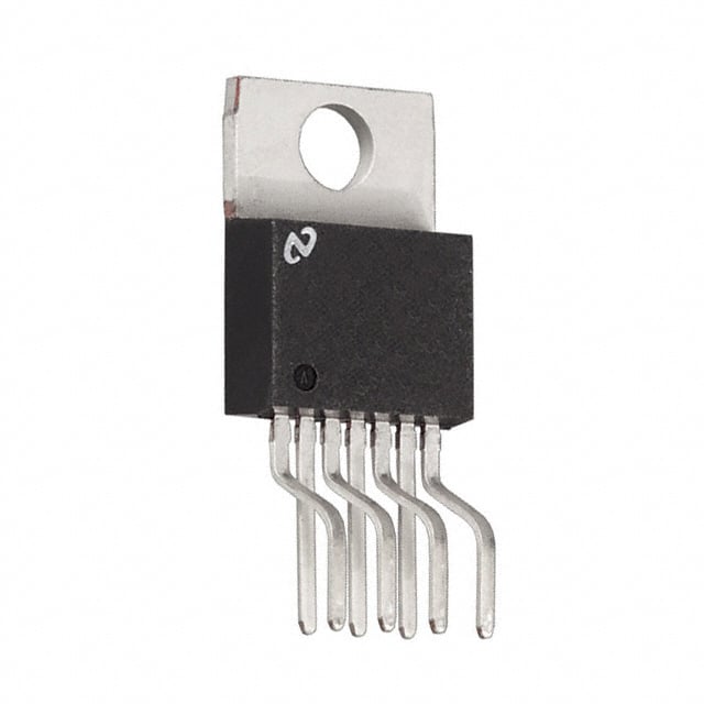
ICGOO电子元器件商城为您提供LM2673T-5.0/NOPB由Texas Instruments设计生产,在icgoo商城现货销售,并且可以通过原厂、代理商等渠道进行代购。 LM2673T-5.0/NOPB价格参考¥14.60-¥29.91。Texas InstrumentsLM2673T-5.0/NOPB封装/规格:PMIC - 稳压器 - DC DC 开关稳压器, 固定 降压 开关稳压器 IC 正 5V 1 输出 3A TO-220-7(成形引线)。您可以下载LM2673T-5.0/NOPB参考资料、Datasheet数据手册功能说明书,资料中有LM2673T-5.0/NOPB 详细功能的应用电路图电压和使用方法及教程。
LM2673T-5.0/NOPB 是 Texas Instruments(德州仪器)推出的一款 PMIC(电源管理集成电路),属于 DC-DC 开关稳压器系列。该器件具有高效、低功耗的特点,适用于多种需要稳定直流电压输出的应用场景。以下是其主要应用场景及特点:

 1. 消费类电子产品
   - LM2673T-5.0/NOPB 可为便携式设备提供稳定的 5V 输出,适用于智能手机充电器、平板电脑适配器、蓝牙耳机充电盒等。
   - 在这些设备中,它能够将较高的输入电压(如 12V 或 24V)转换为所需的 5V 输出,同时保持高效率和低发热。

 2. 工业控制
   - 该稳压器适合用于工业自动化设备中的电源模块,例如 PLC(可编程逻辑控制器)、传感器接口电路和数据采集系统。
   - 它的宽输入电压范围(9V 至 40V)和高达 3A 的负载能力,使其能够适应复杂的工业环境。

 3. 通信设备
   - 在网络路由器、交换机和基站设备中,LM2673T-5.0/NOPB 可以用作辅助电源,为微控制器、FPGA 和其他数字电路供电。
   - 其开关频率固定为 100kHz,有助于简化滤波设计并减少电磁干扰(EMI)。

 4. 汽车电子
   - 虽然 LM2673T-5.0/NOPB 不是专门针对汽车级应用设计,但在某些非关键车载系统中(如导航仪、倒车摄像头或娱乐系统),它可以作为电源解决方案。
   - 它能够承受较大的电压波动,并在启动瞬间提供稳定的电流输出。

 5. 电池供电设备
   - 对于依赖电池运行的设备(如手持扫描仪、无线键盘鼠标或便携式医疗仪器),这款稳压器可以延长电池寿命,因为它具备高效率和较低的静态电流。

 6. LED 驱动
   - LM2673T-5.0/NOPB 还可用于驱动中小功率 LED 灯串,特别是在需要恒定电压输出的情况下。
   - 它支持降压模式操作,确保 LED 的亮度一致且不受输入电压变化的影响。

 总结
LM2673T-5.0/NOPB 凭借其高效能、高可靠性以及易于设计的特点,在消费电子、工业控制、通信设备和电池供电系统等领域有着广泛的应用前景。其固定的 5V 输出和强大的负载能力,使其成为许多现代电子产品的理想选择。
| 参数 | 数值 |
| 产品目录 | 集成电路 (IC)半导体 |
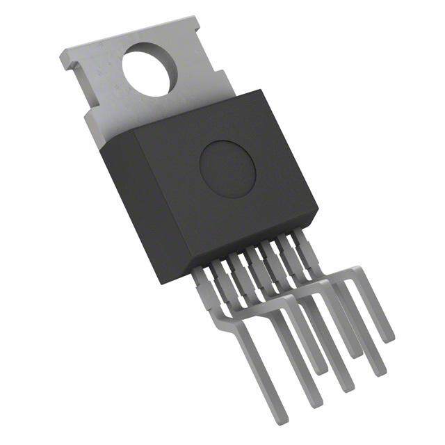
| 描述 | IC REG BUCK 5V 3A TO220-7稳压器—开关式稳压器 3A SD VTG Reg w/ Adj Crnt Limit |
| 产品分类 | |
| 品牌 | Texas Instruments |
| 产品手册 | http://www.ti.com/litv/snvs030n |
| 产品图片 |
|
| rohs | 符合RoHS无铅 / 符合限制有害物质指令(RoHS)规范要求 |
| 产品系列 | 电源管理 IC,稳压器—开关式稳压器,Texas Instruments LM2673T-5.0/NOPBSIMPLE SWITCHER® |
| 数据手册 | |
| 产品型号 | LM2673T-5.0/NOPB |
| PWM类型 | - |
| 产品培训模块 | http://www.digikey.cn/PTM/IndividualPTM.page?site=cn&lang=zhs&ptm=30128 |
| 产品目录页面 | |
| 产品种类 | 稳压器—开关式稳压器 |
| 供应商器件封装 | TO-220-7 |
| 其它名称 | *LM2673T-5.0/NOPB |
| 制造商产品页 | http://www.ti.com/general/docs/suppproductinfo.tsp?distId=10&orderablePartNumber=LM2673T-5.0/NOPB |
| 包装 | 管件 |
| 同步整流器 | 无 |
| 商标 | Texas Instruments |
| 安装类型 | 通孔 |
| 安装风格 | Through Hole |
| 封装 | Tube |
| 封装/外壳 | TO-220-7 成形引线 |
| 封装/箱体 | TO-220-7 |
| 工作温度 | -40°C ~ 125°C |
| 工厂包装数量 | 45 |
| 开关频率 | 260 kHz |
| 最大工作温度 | + 125 C |
| 最大输入电压 | 40 V |
| 最小工作温度 | - 40 C |
| 最小输入电压 | 8 V |
| 标准包装 | 45 |
| 电压-输入 | 8 V ~ 40 V |
| 电压-输出 | 5V |
| 电流-输出 | 3A |
| 类型 | 降压(降压) |
| 系列 | LM2673 |
| 设计资源 | http://www.digikey.com/product-highlights/cn/zh/texas-instruments-webench-design-center/3176 |
| 输出数 | 1 |
| 输出电压 | 5 V |
| 输出电流 | 3 A |
| 输出端数量 | 1 Output |
| 输出类型 | 固定 |
| 配用 | /product-detail/zh/LM2673-5.0EVAL/LM2673-5.0EVAL-ND/366896 |
| 频率-开关 | 260kHz |


- 商务部:美国ITC正式对集成电路等产品启动337调查
- 曝三星4nm工艺存在良率问题 高通将骁龙8 Gen1或转产台积电
- 太阳诱电将投资9.5亿元在常州建新厂生产MLCC 预计2023年完工
- 英特尔发布欧洲新工厂建设计划 深化IDM 2.0 战略
- 台积电先进制程称霸业界 有大客户加持明年业绩稳了
- 达到5530亿美元!SIA预计今年全球半导体销售额将创下新高
- 英特尔拟将自动驾驶子公司Mobileye上市 估值或超500亿美元
- 三星加码芯片和SET,合并消费电子和移动部门,撤换高东真等 CEO
- 三星电子宣布重大人事变动 还合并消费电子和移动部门
- 海关总署:前11个月进口集成电路产品价值2.52万亿元 增长14.8%


PDF Datasheet 数据手册内容提取
Product Sample & Technical Tools & Support & Folder Buy Documents Software Community LM2673 SNVS030O–APRIL2000–REVISEDJUNE2016 ® LM2673 SIMPLE SWITCHER 3-A Step-Down Voltage Regulator With Adjustable Current Limit 1 Features 3 Description • EfficiencyUpto94% The LM2673 series of regulators are monolithic 1 integrated circuits which provide all of the active • SimpleandEasytoDesignWith(UsingOff-The- functions for a step-down (buck) switching regulator ShelfExternalComponents) capable of driving up to 3-A loads with excellent line • ResistorProgrammablePeakCurrentLimitOvera and load regulation characteristics. High efficiency Rangeof2Ato5A (>90%) is obtained through the use of a low ON- resistance DMOS power switch. The series consists • 150-mΩDMOSOutputSwitch of fixed output voltages of 3.3 V, 5 V, and 12 V and • 3.3-V,5-V,12-VFixedOutputandAdjustable anadjustableoutputversion. (1.2Vto37V)Versions The SIMPLE SWITCHER® concept provides for a • ±2%MaximumOutputToleranceOverFullLine complete design using a minimum number of external andLoadConditions components. A high fixed frequency oscillator • WideInputVoltageRange:8Vto40V (260 kHz) allows the use of physically smaller sized • 260-KHzFixedFrequencyInternalOscillator components. A family of standard inductors for use with the LM2673 are available from several • Soft-StartCapability manufacturerstogreatlysimplifythedesignprocess. • –40to125°COperatingJunctionTemperature Range Other features include the ability to reduce the input surge current at power on by adding a soft-start timing capacitor to gradually turn on the regulator. 2 Applications The LM2673 series also has built-in thermal • Simple-to-Design,HighEfficiency(>90%)Step- shutdown and resistor programmable current limit of DownSwitchingRegulators the power MOSFET switch to protect the device and load circuitry under fault conditions. The output • EfficientSystemPreregulatorforLinearVoltage voltage is ensured to a ±2% tolerance. The clock Regulators frequencyiscontrolledtowithina±11%tolerance. • BatteryChargers DeviceInformation(1) PARTNUMBER PACKAGE BODYSIZE(NOM) TO-263(7) 10.10mm×8.89mm LM2673 TO-220(7) 14.986mm×10.16mm VSON(14) 6.00mm×5.00mm (1) For all available packages, see the orderable addendum at theendofthedatasheet. TypicalApplication Feedback 0.01 PF Input VIN Voltage LM2673 - 5.0 Boost Output 8V to 40V 0.47 PF L Voltage CIN + + Switch 33 PH 5V/3A 2 x 15 PF/50V Softstart Current Ground Output + COUT 8.2k Limit SR305 180 PF/16V 1 nF Adjust 37,125 ICL = RADJ Copyright © 2016, Texas Instruments Incorporated 1 An IMPORTANT NOTICE at the end of this data sheet addresses availability, warranty, changes, use in safety-critical applications, intellectualpropertymattersandotherimportantdisclaimers.PRODUCTIONDATA.
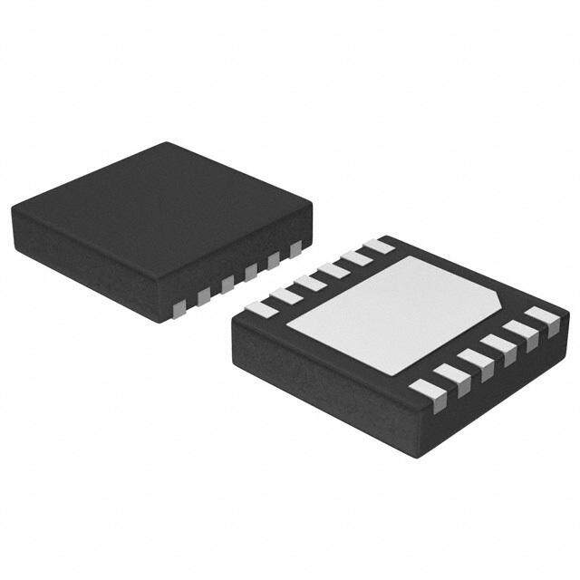
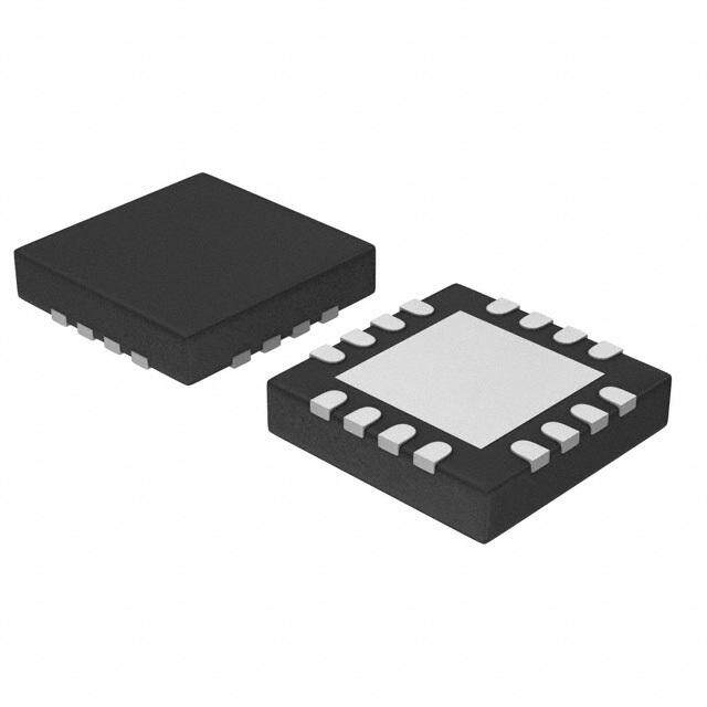
LM2673 SNVS030O–APRIL2000–REVISEDJUNE2016 www.ti.com Table of Contents 1 Features.................................................................. 1 7.3 FeatureDescription...................................................9 2 Applications........................................................... 1 7.4 DeviceFunctionalModes........................................10 3 Description............................................................. 1 8 ApplicationandImplementation........................ 11 4 RevisionHistory..................................................... 2 8.1 ApplicationInformation............................................11 8.2 TypicalApplications................................................14 5 PinConfigurationandFunctions......................... 3 9 PowerSupplyRecommendations...................... 26 6 Specifications......................................................... 4 10 Layout................................................................... 26 6.1 AbsoluteMaximumRatings......................................4 6.2 ESDRatings..............................................................4 10.1 LayoutGuidelines.................................................26 6.3 RecommendedOperatingConditions.......................4 10.2 LayoutExample....................................................27 6.4 ThermalInformation..................................................5 11 DeviceandDocumentationSupport................. 28 6.5 ElectricalCharacteristics:LM2673–3.3V...............5 11.1 RelatedDocumentation.........................................28 6.6 ElectricalCharacteristics:LM2673–5V..................5 11.2 ReceivingNotificationofDocumentationUpdates28 6.7 ElectricalCharacteristics:LM2673–12V................6 11.3 CommunityResources..........................................28 6.8 ElectricalCharacteristics:LM2673–Adjustable.......6 11.4 Trademarks...........................................................28 6.9 ElectricalCharacteristics–AllOutputVoltage 11.5 ElectrostaticDischargeCaution............................28 Versions.....................................................................6 11.6 Glossary................................................................28 6.10 TypicalCharacteristics............................................7 12 Mechanical,Packaging,andOrderable 7 DetailedDescription.............................................. 9 Information........................................................... 28 7.1 Overview...................................................................9 12.1 DAP(VSONPackage)..........................................28 7.2 FunctionalBlockDiagram.........................................9 4 Revision History NOTE:Pagenumbersforpreviousrevisionsmaydifferfrompagenumbersinthecurrentversion. ChangesfromRevisionN(April2013)toRevisionO Page • AddedESDRatingstable,FeatureDescriptionsection,DeviceFunctionalModes,ApplicationandImplementation section,PowerSupplyRecommendationssection,Layoutsection,DeviceandDocumentationSupportsection,and Mechanical,Packaging,andOrderableInformationsection.................................................................................................. 1 • RemovedallreferencestoComputerDesignSoftwareLM267XMadeSimple(Version6.0).............................................. 1 ChangesfromRevisionM(April2013)toRevisionN Page • ChangedlayoutofNationalDataSheettoTIformat........................................................................................................... 24 2 SubmitDocumentationFeedback Copyright©2000–2016,TexasInstrumentsIncorporated ProductFolderLinks:LM2673
LM2673 www.ti.com SNVS030O–APRIL2000–REVISEDJUNE2016 5 Pin Configuration and Functions KTWPackage 7-PinTO-263 NDZPackage TopView 7-PinTO-220 TopView Not to scale 7 SS 6 FB 5 Current_adjust 4 GND 3 CB 2 Input 1234567 1 Switch_output Not to scale putputCBNDustFBSS outIn Gadj _ _ Switch Current NHMPackage 14-PinVSON TopView NC 1 14 Switch_output Input 2 13 Switch_output Input 3 12 Switch_output CB 4 DAP 11 NC NC 5 10 NC Current_adjust 6 9 GND FB 7 8 SS Not to scale ConnectDAPtopin9onPCB. PinFunctions PIN TO-263, I/O DESCRIPTION NAME VSON TO-220 SourcepinoftheinternalHighSideFET.Thisisaswitchingnode.Attachedthispinto Switchoutput 1 12,13,14 O aninductorandthecathodeoftheexternaldiode. SupplyinputpintocollectorpinofhighsideFET.Connecttopowersupplyandinput Input 2 2,3 I bypasscapacitorsCIN.PathfromVINpintohighfrequencybypassCINandGND mustbeasshortaspossible. Boot-strapcapacitorconnectionforhigh-sidedriver.Connectahighquality100-nF CB 3 4 I capacitorfromCBtoVSWPin. Powergroundpins.Connecttosystemground.GroundpinsofCINandCOUT.Pathto GND 4 9 — CINmustbeasshortaspossible. CurrentLimitadjustpin.ConnectaresistorfromthispintoGNDtosetthecurrentlimit Currentadjust 5 6 I ofthepart. Feedbacksenseinputpin.ConnecttothemidpointoffeedbackdividertosetVOUTfor FB 6 7 I ADJversionorconnectthispindirectlytotheoutputcapacitorforafixedoutput version. Soft-startpin.ConnectacapacitorfromthispintoGNDtocontroltheoutputvoltage SS 7 8 I ramp.Ifthefeaturenotdesired,thepincanbeleftfloating NC — 1,5,10,11 — Noconnectpins Copyright©2000–2016,TexasInstrumentsIncorporated SubmitDocumentationFeedback 3 ProductFolderLinks:LM2673
LM2673 SNVS030O–APRIL2000–REVISEDJUNE2016 www.ti.com 6 Specifications 6.1 Absolute Maximum Ratings(1)(2) MIN MAX UNIT Inputsupplyvoltage 45 V Soft-startpinvoltage –0.1 6 V Switchvoltagetoground(3) –1 V V IN V +8 Boostpinvoltage SW V V Feedbackpinvoltage –0.3 14 V Powerdissipation InternallyLimited Wave,4s 260 Solderingtemperature Infrared,10s 240 °C Vaporphase,75s 219 Storagetemperature,T –65 150 °C stg (1) StressesbeyondthoselistedunderAbsoluteMaximumRatingsmaycausepermanentdamagetothedevice.Thesearestressratings only,whichdonotimplyfunctionaloperationofthedeviceattheseoranyotherconditionsbeyondthoseindicatedunderRecommended OperatingConditions.Exposuretoabsolute-maximum-ratedconditionsforextendedperiodsmayaffectdevicereliability. (2) IfMilitary/Aerospacespecifieddevicesarerequired,pleasecontacttheTexasInstrumentsSalesOffice/Distributorsforavailabilityand specifications. (3) TheabsolutemaximumspecificationoftheSwitchVoltagetoGroundappliestoDCvoltage.Anextendednegativevoltagelimitof–10V appliestoapulseofupto20ns,–6Vof60nsand–3Vofupto100ns. 6.2 ESD Ratings VALUE UNIT V Electrostaticdischarge Human-bodymodel(HBM),perANSI/ESDA/JEDECJS-001(1)(2) ±2000 V (ESD) (1) JEDECdocumentJEP155statesthat500-VHBMallowssafemanufacturingwithastandardESDcontrolprocess. (2) ESDwasappliedusingthehuman-bodymodel,a100-pFcapacitordischargedthrougha1.5-kΩresistorintoeachpin. 6.3 Recommended Operating Conditions MIN MAX UNIT Supplyvoltage 8 40 V Junctiontemperature(T) –40 125 °C J 4 SubmitDocumentationFeedback Copyright©2000–2016,TexasInstrumentsIncorporated ProductFolderLinks:LM2673
LM2673 www.ti.com SNVS030O–APRIL2000–REVISEDJUNE2016 6.4 Thermal Information LM2678 THERMALMETRIC(1) NDZ(TO-220) KTW(TO-263) NHM(VSON) UNIT 7PINS 7PINS 14PINS See (2) 65 — — See (3) 45 — — See (4) — 56 — R Junction-to-ambientthermalresistance See (5) — 35 — °C/W θJA See (6) — 26 — See (7) — — 55 See (8) — — 29 R Junction-to-case(top)thermalresistance 2 2 — °C/W θJC(top) (1) Formoreinformationabouttraditionalandnewthermalmetrics,seetheSemiconductorandICPackageThermalMetricsapplication report. (2) Junctiontoambientthermalresistance(noexternalheatsink)forthe7-leadTO-220packagemountedvertically,with½inchleadsina socket,oronaPCBwithminimumcopperarea. (3) Junctiontoambientthermalresistance(noexternalheatsink)forthe7-leadTO-220packagemountedvertically,with½inchleads solderedtoaPCBcontainingapproximately4squareinchesof(1oz.)copperareasurroundingtheleads. (4) Junctiontoambientthermalresistanceforthe7-leadDDPAKmountedhorizontallyagainstaPCBareaof0.136squareinches(the samesizeastheDDPAKpackage)of1oz.(0.0014in.thick)copper. (5) Junctiontoambientthermalresistanceforthe7-leadDDPAKmountedhorizontallyagainstaPCBareaof0.4896squareinches(3.6 timestheareaoftheDDPAKpackage)of1oz.(0.0014in.thick)copper. (6) Junctiontoambientthermalresistanceforthe7-leadDDPAKmountedhorizontallyagainstaPCBcopperareaof1.0064squareinches (7.4timestheareaoftheDDPAK3package)of1oz.(0.0014in.thick)copper.Additionalcopperareawillreducethermalresistance further. (7) Junctiontoambientthermalresistanceforthe14-leadVSONmountedonaPCBcopperareaequaltothedieattachpaddle. (8) Junctiontoambientthermalresistanceforthe14-leadVSONmountedonaPCBcopperareausing12viastoasecondlayerofcopper equaltodieattachpaddle.Additionalcopperareawillreducethermalresistancefurther.Forlayoutrecommendations,seeApplication NoteAN-1187LeadlessLeadframPackage(LLP). 6.5 Electrical Characteristics: LM2673 – 3.3 V SpecificationsapplyforT =T =25°Cunlessotherwisenoted.R =5.6kΩ. A J ADJ PARAMETER TESTCONDITIONS MIN(1) TYP(2) MAX(1) UNIT 3.234 3.3 3.366 V =8Vto40V, VOUT Outputvoltage 10IN0mA≤IOUT≤5A overtheentirejunctiontemperature 3.201 3.399 V rangeofoperation–40°Cto125°C η Efficiency V =12V,I =5A 86% IN LOAD (1) Allroomtemperaturelimitsare100%testedduringproductionwithT =T =25°C.Alllimitsattemperatureextremesarespecifiedvia A J correlationusingstandardQualityControl(SQC)methods.AlllimitsareusedtocalculateAverageOutgoingQualityLevel(AOQL). (2) TypicalvaluesaredeterminedwithT =T =25°Candrepresentthemostlikelynorm. A J 6.6 Electrical Characteristics: LM2673 – 5 V PARAMETER TESTCONDITIONS MIN(1) TYP(2) MAX(1) UNIT 4.9 5 5.1 V =8Vto40V, VOUT Outputvoltage 10IN0mA≤IOUT≤5A overtheentirejunctiontemperature 4.85 5.15 V rangeofoperation–40°Cto125°C η Efficiency V =12V,I =5A 88% IN LOAD (1) Allroomtemperaturelimitsare100%testedduringproductionwithT =T =25°C.Alllimitsattemperatureextremesarespecifiedvia A J correlationusingstandardQualityControl(SQC)methods.AlllimitsareusedtocalculateAverageOutgoingQualityLevel(AOQL). (2) TypicalvaluesaredeterminedwithT =T =25°Candrepresentthemostlikelynorm. A J Copyright©2000–2016,TexasInstrumentsIncorporated SubmitDocumentationFeedback 5 ProductFolderLinks:LM2673
LM2673 SNVS030O–APRIL2000–REVISEDJUNE2016 www.ti.com 6.7 Electrical Characteristics: LM2673 – 12 V PARAMETER TESTCONDITIONS MIN(1) TYP(2) MAX(1) UNIT 11.76 12 12.24 VOUT Outputvoltage V10IN0=m1A5≤VIOtoUT40≤V5,A overtheentirejunctiontemperaturerange 11.64 12.36 V ofoperation–40°Cto125°C η Efficiency VIN=24V,ILOAD=5A 94% (1) Allroomtemperaturelimitsare100%testedduringproductionwithT =T =25°C.Alllimitsattemperatureextremesarespecifiedvia A J correlationusingstandardQualityControl(SQC)methods.AlllimitsareusedtocalculateAverageOutgoingQualityLevel(AOQL). (2) TypicalvaluesaredeterminedwithT =T =25°Candrepresentthemostlikelynorm. A J 6.8 Electrical Characteristics: LM2673 – Adjustable PARAMETER TESTCONDITIONS MIN(1) TYP(2) MAX(1) UNIT VIN=8Vto40V, 1.186 1.21 1.234 VFB Feedbackvoltage 100mA≤IOUT≤5A, overtheentirejunctiontemperaturerange V VOUTprogrammedfor5V ofoperation–40°Cto125°C 1.174 1.246 η Efficiency VIN=12V,ILOAD=5A 88% (1) Allroomtemperaturelimitsare100%testedduringproductionwithT =T =25°C.Alllimitsattemperatureextremesarespecifiedvia A J correlationusingstandardQualityControl(SQC)methods.AlllimitsareusedtocalculateAverageOutgoingQualityLevel(AOQL). (2) TypicalvaluesaredeterminedwithT =T =25°Candrepresentthemostlikelynorm. A J 6.9 Electrical Characteristics – All Output Voltage Versions SpecificationsareforT =T =25°Cunlessotherwisespecified.UnlessotherwisespecifiedV =12Vforthe3.3-V,5-V,and A J IN AdjustableversionsandV =24Vforthe12-Vversion. IN PARAMETER TESTCONDITIONS MIN TYP MAX UNIT DEVICEPARAMETERS IQ Quiescentcurrent VVFFEEEEDDBBAACCKK==815VVfoforr31.32--VV,5ve-Vrs,ioannsdADJversions, 4.2 6 mA 1.181 1.21 1.229 Currentlimitadjust VADJ voltage overtheentirejunctiontemperaturerangeofoperation–40°Cto 1.169 1.246 V 125°C 5.5 6.3 7.6 ICL Currentlimit RADJ=5.6kΩ,(1) overtheentirejunctiontemperaturerange A 5.3 8.1 ofoperation–40°Cto125°C IL Outputleakagecurrent VsoINft-=st4a0rtVp,in=0V VVSSWWIITTCCHH==–01VV 16 11.55 mA 0.12 0.14 RDS(ON) SwitchON-resistance ISWITCH=5A overtheentirejunctiontemperaturerange Ω 0.225 ofoperation–40°Cto125°C 260 fO Oscillatorfrequency Measuredatswitchpin overtheentirejunctiontemperaturerange kHz 225 280 ofoperation–40°Cto125°C Maximumdutycycle 91% D Dutycycle Minimumdutycycle 0% IBIAS Fcuererdebnatckbias VAFDEJEDvBeArCsKio=n1o.n3lyV 85 nA 0.63 Soft-startthreshold VSFST voltage overtheentirejunctiontemperaturerangeofoperation–40°Cto 0.53 0.74 V 125°C 3.7 ISFST Soft-startpincurrent Soft-startpin=0V overtheentirejunctiontemperaturerange µA 6.9 ofoperation–40°Cto125°C (1) Thepeakswitchcurrentlimitisdeterminedbythefollowingrelationship:I =37,125/R . CL ADJ 6 SubmitDocumentationFeedback Copyright©2000–2016,TexasInstrumentsIncorporated ProductFolderLinks:LM2673
LM2673 www.ti.com SNVS030O–APRIL2000–REVISEDJUNE2016 6.10 Typical Characteristics Figure1.NormalizedOutputVoltage Figure2.LineRegulation Figure3.EfficiencyvsInputVoltage Figure4.EfficiencyvsI LOAD Figure5.SwitchCurrentLimit Figure6.OperatingQuiescentCurrent Copyright©2000–2016,TexasInstrumentsIncorporated SubmitDocumentationFeedback 7 ProductFolderLinks:LM2673
LM2673 SNVS030O–APRIL2000–REVISEDJUNE2016 www.ti.com Typical Characteristics (continued) Figure7.SwitchingFrequency Figure8.FeedbackPinBiasCurrent ContinuousModeSwitchingWaveformsVIN=20V, DiscontinuousModeSwitchingWaveformsVIN=20V, VOUT=5V,ILOAD=3AL=33µH,COUT=200µF, VOUT=5V,ILOAD=500mAL=10µH,COUT=400µF, COUTESR=26mΩ COUTESR=13mΩ A:VSWPinVoltage,10V/div A:VSWPinVoltage,10V/div B:InductorCurrent,1A/div B:InductorCurrent,1A/div C:OutputRippleVoltage,20mV/divAC-Coupled C:OutputRippleVoltage,20mV/divAC-Coupled Figure9.HorizontalTimeBase:1µs/div Figure10.HorizontalTimeBase:1µs//iv LoadTransientResponseforContinuousModeVIN=20V, LoadTransientResponseforDiscontinuousModeVIN=20V, VOUT=5VL=33µH,COUT=200µF,COUTESR=26mΩ VOUT=5V,L=10µH,COUT=400µF,COUTESR=13mΩ A:OutputVoltage,100mV//div,AC-Coupled. A:OutputVoltage,100mV/div,AC-Coupled. B:LoadCurrent:500-mAto3-ALoadPulse B:LoadCurrent:200-mAto3-ALoadPulse Figure11.HorizontalTimeBase:100µs/div Figure12.HorizontalTimeBase:200µs/div 8 SubmitDocumentationFeedback Copyright©2000–2016,TexasInstrumentsIncorporated ProductFolderLinks:LM2673
LM2673 www.ti.com SNVS030O–APRIL2000–REVISEDJUNE2016 7 Detailed Description 7.1 Overview The LM2673 provides all of the active functions required for a step-down (buck) switching regulator. The internal powerswitchisaDMOSpowerMOSFETtoprovidepowersupplydesignswithhighcurrentcapability,upto3A, andhighlyefficientoperation. The design support WEBENCH, can also be used to provide instant component selection, circuit performance calculationsforevaluation,abillofmaterialscomponentlistandacircuitschematicforLM2673. 7.2 Functional Block Diagram *ActiveInductorPatentNumber5,514,947 †ActiveCapacitorPatentNumber5,382,918 7.3 Feature Description 7.3.1 SwitchOutput ThisistheoutputofapowerMOSFETswitchconnecteddirectlytotheinputvoltage.Theswitchprovidesenergy to an inductor, an output capacitor and the load circuitry under control of an internal pulse-width-modulator (PWM). The PWM controller is internally clocked by a fixed 260-kHz oscillator. In a standard step-down application the duty cycle (Time ON/Time OFF) of the power switch is proportional to the ratio of the power supply output voltage to the input voltage. The voltage on pin 1 switches between V (switch ON) and below IN groundbythevoltagedropoftheexternalSchottkydiode(switchOFF). Copyright©2000–2016,TexasInstrumentsIncorporated SubmitDocumentationFeedback 9 ProductFolderLinks:LM2673
LM2673 SNVS030O–APRIL2000–REVISEDJUNE2016 www.ti.com Feature Description (continued) 7.3.2 Input The input voltage for the power supply is connected to pin 2. In addition to providing energy to the load the input voltage also provides bias for the internal circuitry of the LM2673. For ensured performance the input voltage must be in the range of 8 V to 40 V. For best performance of the power supply the input pin must always be bypassedwithaninputcapacitorlocatedclosetopin2. 7.3.3 CBoost A capacitor must be connected from pin 3 to the switch output, pin 1. This capacitor boosts the gate drive to the internal MOSFET above V to fully turn it ON. This minimizes conduction losses in the power switch to maintain IN highefficiency.TherecommendedvalueforCBoostis0.01 µF. 7.3.4 Ground This is the ground reference connection for all components in the power supply. In fast-switching, high-current applications such as those implemented with the LM2673, TI recommends that a broad ground plane be used to minimizesignalcouplingthroughoutthecircuit. 7.3.5 CurrentAdjust A key feature of the LM2673 is the ability to tailor the peak switch current limit to a level required by a particular application. This alleviates the need to use external components that must be physically sized to accommodate current levels (under shorted output conditions for example) that may be much higher than the normal circuit operatingcurrentrequirements. A resistor connected from pin 5 to ground establishes a current (I = 1.2 V / R ) that sets the peak current (pin 5) ADJ throughthepowerswitch.Themaximumswitchcurrentisfixedatalevelof37,125/R . ADJ 7.3.6 Feedback This is the input to a two-stage high gain amplifier, which drives the PWM controller. It is necessary to connect pin6totheactualoutputofthepowersupplytosettheDCoutputvoltage.Forthefixedoutputdevices(3.3-V,5- V, and 12-V outputs), a direct wire connection to the output is all that is required as internal gain setting resistors are provided inside the LM2673. For the adjustable output version two external resistors are required to set the dc output voltage. For stable operation of the power supply it is important to prevent coupling of any inductor flux tothefeedbackinput. 7.4 Device Functional Modes 7.4.1 Soft-Start Acapacitorconnectedfrompin7togroundallowsforaslowturnonoftheswitchingregulator.Thecapacitorsets a time delay to gradually increase the duty cycle of the internal power switch. This can significantly reduce the amount of surge current required from the input supply during an abrupt application of the input voltage. If soft start is not required this pin must be left open circuited. See C Soft-Start Capacitor for further information SS regardingsoft-startcapacitorvalues. 10 SubmitDocumentationFeedback Copyright©2000–2016,TexasInstrumentsIncorporated ProductFolderLinks:LM2673
LM2673 www.ti.com SNVS030O–APRIL2000–REVISEDJUNE2016 8 Application and Implementation NOTE Information in the following applications sections is not part of the TI component specification, and TI does not warrant its accuracy or completeness. TI’s customers are responsible for determining suitability of components for their purposes. Customers should validateandtesttheirdesignimplementationtoconfirmsystemfunctionality. 8.1 Application Information 8.1.1 DesignConsiderations PowersupplydesignusingtheLM2673isgreatlysimplifiedbyusingrecommendedexternalcomponents.Awide range of inductors, capacitors and Schottky diodes from several manufacturers have been evaluated for use in designs that cover the full range of capabilities (input voltage, output voltage, and load current) of the LM2673. A simple design procedure using nomographs and component tables provided in this data sheet leads to a working designwithverylittleeffort. The individual components from the various manufacturers called out for use are still just a small sample of the vast array of components available in the industry. While these components are recommended, they are not exclusively the only components for use in a design. After a close comparison of component specifications, equivalentdevicesfromothermanufacturerscouldbesubstitutedforuseinanapplication. Important considerations for each external component and an explanation of how the nomographs and selection tablesweredevelopedfollows. 8.1.2 Inductor The inductor is the key component in a switching regulator. For efficiency the inductor stores energy during the switchONtimeandthentransfersenergytotheloadwhiletheswitchisOFF. Nomographs are used to select the inductance value required for a given set of operating conditions. The nomographs assume that the circuit is operating in continuous mode (the current flowing through the inductor never falls to zero). The magnitude of inductance is selected to maintain a maximum ripple current of 30% of the maximumloadcurrent.Iftheripplecurrentexceedsthis30%limitthenextlargervalueisselected. The inductors offered have been specifically manufactured to provide proper operation under all operating conditions of input and output voltage and load current. Several part types are offered for a given amount of inductance. Both surface mount and through-hole devices are available. The inductors from each of the three manufacturershaveuniquecharacteristics. • Renco: ferrite stick core inductors; benefits are typically lowest cost and can withstand ripple and transient peak currents above the rated value. These inductors have an external magnetic field, which may generate EMI. • Pulse Engineering: powdered iron toroid core inductors; these also can withstand higher than rated currents and,beingtoroidinductors,haslowEMI. • Coilcraft: ferrite drum core inductors; these are the smallest physical size inductors and are available only as surfacemountcomponents.TheseinductorsalsogenerateEMIbutlessthanstickinductors. 8.1.3 OutputCapacitor The output capacitor acts to smooth the dc output voltage and also provides energy storage. Selection of an output capacitor, with an associated equivalent series resistance (ESR), impacts both the amount of output ripple voltageandstabilityofthecontrolloop. The output ripple voltage of the power supply is the product of the capacitor ESR and the inductor ripple current. ThecapacitortypesrecommendedinthetableswereselectedforhavinglowESRratings. Inaddition,bothsurfacemounttantalumcapacitorsandthrough-holealuminumelectrolyticcapacitorsareoffered assolutions. Copyright©2000–2016,TexasInstrumentsIncorporated SubmitDocumentationFeedback 11 ProductFolderLinks:LM2673
LM2673 SNVS030O–APRIL2000–REVISEDJUNE2016 www.ti.com Application Information (continued) Impacting frequency stability of the overall control loop, the output capacitance, in conjunction with the inductor, creates a double pole inside the feedback loop. In addition the capacitance and the ESR value create a zero. These frequency response effects together with the internal frequency compensation circuitry of the LM2673 modifythegainandphaseshiftoftheclosedloopsystem. As a general rule for stable switching regulator circuits it is desired to have the unity gain bandwidth of the circuit to be limited to no more than one-sixth of the controller switching frequency. With the fixed 260-kHz switching frequency of the LM2673, the output capacitor is selected to provide a unity gain bandwidth of 40 kHz (maximum).Eachrecommendedcapacitorvaluehasbeenchosentoachievethisresult. In some cases multiple capacitors are required either to reduce the ESR of the output capacitor, to minimize output ripple (a ripple voltage of 1% of V or less is the assumed performance condition), or to increase the OUT output capacitance to reduce the closed-loop unity gain bandwidth, to less than 40 kHz. When parallel combinationsofcapacitorsarerequiredithasbeenassumedthateachcapacitoristheexactsameparttype. TheRMScurrentandworkingvoltage(WV)ratingsoftheoutputcapacitorarealsoimportantconsiderations.Ina typical step-down switching regulator, the inductor ripple current (set to be no more than 30% of the maximum load current by the inductor selection) is the current that flows through the output capacitor. The capacitor RMS current rating must be greater than this ripple current. The voltage rating of the output capacitor must be greater than 1.3 times the maximum output voltage of the power supply. If operation of the system at elevated temperaturesisrequired,thecapacitorvoltageratingmaybede-ratedtolessthanthenominalroomtemperature rating. Careful inspection of the manufacturer's specification for de-rating of working voltage with temperature is important. 8.1.4 InputCapacitor Fast changing currents in high current switching regulators place a significant dynamic load on the unregulated power source. An input capacitor helps to provide additional current to the power supply as well as smooth out inputvoltagevariations. Like the output capacitor, the key specifications for the input capacitor are RMS current rating and working voltage. The RMS current flowing through the input capacitor is equal to one-half of the maximum DC load current so the capacitor should be rated to handle this. Paralleling multiple capacitors proportionally increases the current rating of the total capacitance. The voltage rating must also be selected to be 1.3 times the maximum input voltage. Depending on the unregulated input power source, under light load conditions the maximum input voltagecouldbesignificantlyhigherthannormaloperation.Considerthiswhenselectinganinputcapacitor. The input capacitor must be placed very close to the input pin of the LM2673. Due to relative high current operation with fast transient changes, the series inductance of input connecting wires or PCB traces can create ringing signals at the input terminal which could possibly propagate to the output or other parts of the circuitry. It may be necessary in some designs to add a small valued (0.1 µF to 0.47 µF) ceramic type capacitor in parallel withtheinputcapacitortopreventorminimizeanyringing. 8.1.5 CatchDiode WhenthepowerswitchintheLM2673turnsOFF,thecurrentthroughtheinductorcontinuestoflow.Thepathfor this current is through the diode connected between the switch output and ground. This forward biased diode clampstheswitchoutputtoavoltagelessthanground.Thisnegativevoltagemustbegreaterthan –1Vsoalow voltage drop (particularly at high current levels) Schottky diode is recommended. Total efficiency of the entire power supply is significantly impacted by the power lost in the output catch diode. The average current through the catch diode is dependent on the switch duty cycle (D) and is equal to the load current times (1-D). Use of a diode rated for much higher current than is required by the actual application helps to minimize the voltage drop andpowerlossinthediode. During the switch ON time the diode will be reversed biased by the input voltage. The reverse voltage rating of thediodeshouldbeatleast1.3timesgreaterthanthemaximuminputvoltage. 8.1.6 BoostCapacitor The boost capacitor creates a voltage used to overdrive the gate of the internal power MOSFET. This improves efficiency by minimizing the on resistance of the switch and associated power loss. For all applications it is recommendedtousea0.01-µF,50-Vceramiccapacitor. 12 SubmitDocumentationFeedback Copyright©2000–2016,TexasInstrumentsIncorporated ProductFolderLinks:LM2673
LM2673 www.ti.com SNVS030O–APRIL2000–REVISEDJUNE2016 Application Information (continued) 8.1.7 R ,AdjustableCurrentLimit ADJ A key feature of the LM2673 is the ability to control the peak switch current. Without this feature the peak switch current would be internally set to 5 A or higher to accommodate 3-A load current designs. This requires that both the inductor (which could saturate with excessively high currents) and the catch diode be able to safely handle upto5Awhichwouldbeconductedunderloadfaultconditions. If an application only requires a load current of 2 A or so the peak switch current can be set to a limit just over themaximumloadcurrentwiththeadditionofasingleprogrammingresistor.Thisallowstheuseoflesspowerful andmorecost-effectiveinductorsanddiodes. The peak switch current is equal to a factor of 37,125 divided by R . A resistance of 8.2 kΩ sets the current ADJ limittotypically4.5A.Forpredictablecontrolofthecurrentlimit,TIrecommendskeepingthepeakswitchcurrent greater than 1 A. For lower current applications 500-mA and 1-A switching regulators, the LM2674 and LM2672, areavailable. WhenthepowerswitchreachesthecurrentlimitthresholditisimmediatelyturnedOFFandtheinternalswitching frequency is reduced. This extends the OFF time of the switch to prevent a steady-state, high-current condition. As the switch current falls below the current limit threshold, the switch turns back ON. If a load fault continues, the switch again exceeds the threshold and switch back OFF. This results in a low duty cycle pulsing of the powerswitchtominimizetheoverallfaultconditionpowerdissipation. 8.1.8 C Soft-StartCapacitor SS This optional capacitor controls the rate at which the LM2673 starts up at power on. The capacitor is charged linearly by an internal current source. This voltage ramp gradually increases the duty cycle of the power switch until it reaches the normal operating duty cycle defined primarily by the ratio of the output voltage to the input voltage.Thesoft-startturnontimeisprogrammablebytheselectionofC . SS Theformulaforselectingasoft-startcapacitoris: where • I =Soft-startcurrent,3.7µAtypical SST • t =Soft-starttime,fromdesignrequirements SS • V =Soft-startthresholdvoltage,0.63Vtypical SST • V =Outputvoltage,fromdesignrequirements OUT • V =Schottkydiodevoltagedrop,typically0.5V SCHOTTKY • V =Maximuminputvoltage,fromdesignrequirements (1) IN Ifthisfeatureisnotdesired,leavethesoft-startpin(pin7)opencircuited. With certain soft-start capacitor values and operating conditions, the LM2673 can exhibit an overshoot on the output voltage during turnon. Especially when starting up into no load or low load, the soft-start function may not be effective in preventing a larger voltage overshoot on the output. With larger loads or lower input voltages duringstart-upthiseffectisminimized.Inparticular,avoidusingsoft-startcapacitorsbetween0.033 µFand1µF. 8.1.9 AdditionalApplicationInformation When the output voltage is greater than approximately 6 V, and the duty cycle at minimum input voltage is greater than approximately 50%, the designer should exercise caution in selection of the output filter components. When an application designed to these specific operating conditions is subjected to a current limit fault condition, it may be possible to observe a large hysteresis in the current limit. This can affect the output voltage of the device until the load current is reduced sufficiently to allow the current limit protection circuit to resetitself. Copyright©2000–2016,TexasInstrumentsIncorporated SubmitDocumentationFeedback 13 ProductFolderLinks:LM2673
LM2673 SNVS030O–APRIL2000–REVISEDJUNE2016 www.ti.com Application Information (continued) Undercurrentlimitingconditions,theLM267xisdesignedtorespondinthefollowingmanner: 1. At the moment when the inductor current reaches the current limit threshold, the ON-pulse is immediately terminated.Thishappensforanyapplicationcondition. 2. However, the current limit block is also designed to momentarily reduce the duty cycle to below 50% to avoid subharmonicoscillations,whichcouldcausetheinductortosaturate. 3. Thereafter, once the inductor current falls below the current limit threshold, there is a small relaxation time duringwhichthedutycycleprogressivelyrisesbackabove50%tothevaluerequiredtoachieveregulation. If the output capacitance is sufficiently large, it may be possible that as the output tries to recover, the output capacitor charging current is large enough to repeatedly re-trigger the current-limit circuit before the output has fully settled. This condition is exacerbated with higher output voltage settings because the energy requirement of the output capacitor varies as the square of the output voltage (½ CV2), thus requiring an increased charging current. A simple test to determine if this condition might exist for a suspect application is to apply a short circuit across the output of the converter, and then remove the shorted output condition. In an application with properly selectedexternalcomponents,theoutputrecoverssmoothly. Practical values of external components that have been experimentally found to work well under these specific operating conditions are C = 47 µF, L = 22 µH. It should be noted that even with these components, for a OUT device’s current limit of I , the maximum load current under which the possibility of the large current limit CLIM hysteresis can be minimized is I / 2. For example, if the input is 24 V and the set output voltage is 18 V, then CLIM for a desired maximum current of 1.5 A, the current limit of the chosen switcher must be confirmed to be at least 3A. Under extreme overcurrent or short-circuit conditions, the LM267X employs frequency foldback in addition to the current limit. If the cycle-by-cycle inductor current increases above the current limit threshold (due to short circuit or inductor saturation for example) the switching frequency is automatically reduced to protect the IC. Frequency below100kHzistypicalforanextremeshort-circuitcondition. 8.2 Typical Applications 8.2.1 TypicalApplicationforAllOutputVoltageVersions Feedback 0.01 PF Input VIN Voltage LM2673 - 5.0 Boost Output 8V to 40V 0.47 PF L Voltage CIN + + Switch 33 PH 5V/3A 2 x 15 PF/50V Softstart Current Ground Output + COUT 8.2k Limit SR305 180 PF/16V 1 nF Adjust 37,125 ICL = RADJ Copyright © 2016, Texas Instruments Incorporated Figure13. BasicCircuitforAllOutputVoltageVersions 8.2.1.1 DesignRequirements Select the power supply operating conditions and the maximum output current and follow below procedures to findtheexternalcomponentsforLM2673. 14 SubmitDocumentationFeedback Copyright©2000–2016,TexasInstrumentsIncorporated ProductFolderLinks:LM2673
LM2673 www.ti.com SNVS030O–APRIL2000–REVISEDJUNE2016 Typical Applications (continued) 8.2.1.2 DetailedDesignProcedure Using the nomographs and tables in this data sheet (or use the available design software at www.ti.com) a completestep-downregulatorcanbedesignedinafewsimplesteps. Step1:Definethepowersupplyoperatingconditions: • Requiredoutputvoltage • MaximumDCinputvoltage • Maximumoutputloadcurrent Step 2: Set the output voltage by selecting a fixed output LM2673 (3.3-V, 5-V, or 12-V applications) or determine therequiredfeedbackresistorsforusewiththeadjustableLM2673-ADJ Step 3: Determine the inductor required by using one of the four nomographs, Figure 14 through Figure 17. Table3providesaspecificmanufacturerandpartnumberfortheinductor. Step 4: Using Table 5 and Table 6 (fixed output voltage) or Table 9 and Table 10 (adjustable output voltage), determine the output capacitance required for stable operation. Table 1 and Table 10 provide the specific capacitortypefromthemanufacturerofchoice. Step 5: Determine an input capacitor from Table 5and Table 8 for fixed output voltage applications. Use Table 1 or Table 2 to find the specific capacitor type. For adjustable output circuits select a capacitor from Table 1 or Table 2 with a sufficient working voltage (WV) rating greater than V maximum, and an RMS current rating IN greaterthanone-halfthemaximumloadcurrent(2ormorecapacitorsinparallelmayberequired). Step 6:Select an appropriate diode from Table 4. The current rating of the diode must be greater than I LOAD maximumandthereversevoltageratingmustbegreaterthanV maximum. IN Step 7: Include a 0.01-µF, 50-V capacitor for C in the design and then determine the value of a soft-start BOOST capacitorifdesired. Step8:DefineavalueforR tosetthepeakswitchcurrentlimittobeatleast20%greaterthanI maximum ADJ OUT to allow for at least 30% inductor ripple current (±15% of I ). For designs that must operate over the full OUT temperature range the switch current limit should be set to at least 50% greater than I maximum (1.5 × I OUT OUT maximum). 8.2.1.2.1 CapacitorSelectionGuides Table1.InputandOutputCapacitorCodes—SurfaceMount SURFACEMOUNT CAPACITOR REFERENCE AVXTPSSERIES SPRAGUE594DSERIES KEMETT495SERIES CODE C(µF) WV(V) Irms(A) C(µF) WV(V) Irms(A) C(µF) WV(V) Irms(A) C1 330 6.3 1.15 120 6.3 1.1 100 6.3 0.82 C2 100 10 1.1 220 6.3 1.4 220 6.3 1.1 C3 220 10 1.15 68 10 1.05 330 6.3 1.1 C4 47 16 0.89 150 10 1.35 100 10 1.1 C5 100 16 1.15 47 16 1 150 10 1.1 C6 33 20 0.77 100 16 1.3 220 10 1.1 C7 68 20 0.94 180 16 1.95 33 20 0.78 C8 22 25 0.77 47 20 1.15 47 20 0.94 C9 10 35 0.63 33 25 1.05 68 20 0.94 C10 22 35 0.66 68 25 1.6 10 35 0.63 C11 — — — 15 35 0.75 22 35 0.63 C12 — — — 33 35 1 4.7 50 0.66 C13 — — — 15 50 0.9 — — — Copyright©2000–2016,TexasInstrumentsIncorporated SubmitDocumentationFeedback 15 ProductFolderLinks:LM2673
LM2673 SNVS030O–APRIL2000–REVISEDJUNE2016 www.ti.com Table2.InputandOutputCapacitorCodes—ThroughHole THROUGHHOLE CAPACITOR REFERENCE SANYOOS-CONSASERIES SANYOMV-GXSERIES NICHICONPLSERIES PANASONICHFQSERIES CODE C(µF) WV(V) Irms(A) C(µF) WV(V) Irms(A) C(µF) WV(V) Irms(A) C(µF) WV(V) Irms(A) C1 47 6.3 1 1000 6.3 0.8 680 10 0.8 82 35 0.4 C2 150 6.3 1.95 270 16 0.6 820 10 0.98 120 35 0.44 C3 330 6.3 2.45 470 16 0.75 1000 10 1.06 220 35 0.76 C4 100 10 1.87 560 16 0.95 1200 10 1.28 330 35 1.01 C5 220 10 2.36 820 16 1.25 2200 10 1.71 560 35 1.4 C6 33 16 0.96 1000 16 1.3 3300 10 2.18 820 35 1.62 C7 100 16 1.92 150 35 0.65 3900 10 2.36 1000 35 1.73 C8 150 16 2.28 470 35 1.3 6800 10 2.68 2200 35 2.8 C9 100 20 2.25 680 35 1.4 180 16 0.41 56 50 0.36 C10 47 25 2.09 1000 35 1.7 270 16 0.55 100 50 0.5 C11 — — — 220 63 0.76 470 16 0.77 220 50 0.92 C12 — — — 470 63 1.2 680 16 1.02 470 50 1.44 C13 — — — 680 63 1.5 820 16 1.22 560 50 1.68 C14 — — — 1000 63 1.75 1800 16 1.88 1200 50 2.22 C15 — — — — — — 220 25 0.63 330 63 1.42 C16 — — — — — — 220 35 0.79 1500 63 2.51 C17 — — — — — — 560 35 1.43 — — — C18 — — — — — — 2200 35 2.68 — — — C19 — — — — — — 150 50 0.82 — — — C20 — — — — — — 220 50 1.04 — — — C21 — — — — — — 330 50 1.3 — — — C22 — — — — — — 100 63 0.75 — — — C23 — — — — — — 390 63 1.62 — — — C24 — — — — — — 820 63 2.22 — — — C25 — — — — — — 1200 63 2.51 — — — 8.2.1.2.2 InductorSelectionGuide Table3.InductorManufacturerPartNumbers INDUCTOR RENCO PULSEENGINEERING COILCRAFT INDUCTANCE REFERENCE (µH) CURRENT(A) THROUGH SURFACE THROUGH SURFACE SURFACE NUMBER HOLE MOUNT HOLE MOUNT MOUNT L23 33 1.35 RL-5471-7 RL1500-33 PE-53823 PE-53823S DO3316-333 L24 22 1.65 RL-1283-22-43 RL1500-22 PE-53824 PE-53824S DO3316-223 L25 15 2 RL-1283-15-43 RL1500-15 PE-53825 PE-53825S DO3316-153 L29 100 1.41 RL-5471-4 RL-6050-100 PE-53829 PE-53829S DO5022P-104 L30 68 1.71 RL-5471-5 RL6050-68 PE-53830 PE-53830S DO5022P-683 L31 47 2.06 RL-5471-6 RL6050-47 PE-53831 PE-53831S DO5022P-473 L32 33 2.46 RL-5471-7 RL6050-33 PE-53932 PE-53932S DO5022P-333 L33 22 3.02 RL-1283-22-43 RL6050-22 PE-53933 PE-53933S DO5022P-223 L34 15 3.65 RL-1283-15-43 — PE-53934 PE-53934S DO5022P-153 L38 68 2.97 RL-5472-2 — PE-54038 PE-54038S — L39 47 3.57 RL-5472-3 — PE-54039 PE-54039S — L40 33 4.26 RL-1283-33-43 — PE-54040 PE-54040S — L41 22 5.22 RL-1283-22-43 — PE-54041 P0841 — L44 68 3.45 RL-5473-3 — PE-54044 — — L45 10 4.47 RL-1283-10-43 — — P0845 DO5022P-103HC 16 SubmitDocumentationFeedback Copyright©2000–2016,TexasInstrumentsIncorporated ProductFolderLinks:LM2673
LM2673 www.ti.com SNVS030O–APRIL2000–REVISEDJUNE2016 Table4.SchottkyDiodeSelectionTable REVERSE SURFACEMOUNT THROUGHHOLE VOLTAGE (V) 3A 5AORMORE 3A 5AORMORE 1N5820 20 SK32 — — SR302 SK33 1N5821 30 MBRD835L — 30WQ03F 31DQ03 SK34 MBRB1545CT 1N5822 — 30BQ040 MBR340 MBR745 40 30WQ04F 31DQ04 80SQ045 6TQ045S MBRS340 SR403 6TQ045 MBRD340 SK35 MBR350 50ormore — 31DQ05 — 30WQ05F SR305 8.2.1.3 ApplicationCurves ForContinuousModeOperation Figure14.LM2673-3.3 Figure15.LM2673-5 Figure16.LM2673-12 Figure17.LM2673-ADJ Copyright©2000–2016,TexasInstrumentsIncorporated SubmitDocumentationFeedback 17 ProductFolderLinks:LM2673
LM2673 SNVS030O–APRIL2000–REVISEDJUNE2016 www.ti.com 8.2.2 FixedOutputVoltageApplication Figure18. BasicCircuitforFixedOutputVoltageApplications 8.2.2.1 DesignRequirements Select the power supply operating conditions and the maximum output current and follow below procedures to findtheexternalcomponentsforLM2673. 8.2.2.2 DetailedDesignProcedure A system logic power supply bus of 3.3 V is to be generated from a wall adapter which provides an unregulated DC voltage of 13 V to 16 V. The maximum load current is 2.5 A. A soft-start delay time of 50 ms is desired. Through-holecomponentsarepreferred. Step1:Operatingconditionsare: • V =3.3V OUT • V maximum=16V IN • I maximum=2.5A LOAD Step 2: Select an LM2673T-3.3. The output voltage has a tolerance of ±2% at room temperature and ±3% over thefulloperatingtemperaturerange. Step3:Usethenomographforthe3.3-Vdevice,Figure14.Theintersectionofthe16-Vhorizontalline(V max) IN andthe2.5-Averticalline(I max)indicatesthatL33,a22-µHinductor,isrequired. LOAD From Table 3, L33 in a through-hole component is available from Renco with part number RL-1283-22-43 or part numberPE-53933fromPulseEngineering. Step 4: Use Table 5or Table 6 to determine an output capacitor. With a 3.3-V output and a 33-µH inductor there are four through-hole output capacitor solutions with the number of same type capacitors to be paralleled and an identifying capacitor code given. Table 1 or Table 2 provide the actual capacitor characteristics. Any of the followingchoiceswillworkinthecircuit: • 1× 220-µF,10-VSanyoOS-CON(codeC5) • 1× 1000-µF,35-VSanyoMV-GX(codeC10) • 1× 2200-µF,10-VNichiconPL(codeC5) • 1× 1000-µF,35-VPanasonicHFQ(codeC7) Step 5:Use Table 5or Table 8 to select an input capacitor. With 3.3-V output and 22 µH there are three through- holesolutions.ThesecapacitorsprovideasufficientvoltageratingandanRMScurrentratinggreaterthan1.25A (1/2 I max). Again using Table 1 or Table 2 for specific component characteristics the following choices are LOAD suitable: • 1× 1000-µF,63-VSanyoMV-GX(codeC14) • 1× 820-µF,63-VNichiconPL(codeC24) • 1× 560-µF,50-VPanasonicHFQ(codeC13) 18 SubmitDocumentationFeedback Copyright©2000–2016,TexasInstrumentsIncorporated ProductFolderLinks:LM2673
LM2673 www.ti.com SNVS030O–APRIL2000–REVISEDJUNE2016 Step 6: From Table 4 a 3-A or more Schottky diode must be selected. The 20-V rated diodes are sufficient for theapplicationandforthrough-holecomponentstwoparttypesaresuitable: • 1N5820 • SR302 Step 7: A 0.01-µF capacitor will be used for C . For the 50-ms soft-start delay the following parameters are BOOST tobeused: • I :3.7µA SST • t :50mS SS • V :0.63V SST • V :3.3V OUT • V :0.5V SCHOTTKY • V :16V IN UsingV maxensuresthatthesoft-startdelaytimewillbeatleastthedesired50ms. IN Using the formula for C a value of 0.148 µF is determined to be required. Use of a standard value 0.22-µF SS capacitorwillproducemorethansufficientsoft-startdelay. Step8:DetermineavalueforR toprovideapeakswitchcurrentlimitofatleast2.5Aplus50%or3.75A. ADJ (2) Useavalueof10kΩ. 8.2.2.2.1 CapacitorSelection Table5.OutputCapacitorsforFixedOutputVoltageApplication—SurfaceMount(1)(2) SURFACEMOUNT OUTPUT INDUCTANCE AVXTPSSERIES SPRAGUE594DSERIES KEMETT495SERIES VOLTAGE(V) (µH) NO. CCODE NO. CCODE NO. CCODE 10 4 C2 3 C1 4 C4 15 4 C2 3 C1 4 C4 3.3 22 3 C2 2 C7 3 C4 33 2 C2 2 C6 2 C4 10 4 C2 4 C6 4 C4 15 3 C2 2 C7 3 C4 5 22 3 C2 2 C7 3 C4 33 2 C2 2 C3 2 C4 47 2 C2 1 C7 2 C4 10 4 C5 3 C6 5 C9 15 3 C5 2 C7 4 C8 22 2 C5 2 C6 3 C8 12 33 2 C5 1 C7 2 C8 47 2 C4 1 C6 2 C8 68 1 C5 1 C5 2 C7 100 1 C4 1 C5 1 C8 (1) No.representsthenumberofidenticalcapacitortypestobeconnectedinparallel (2) CCodeindicatestheCapacitorReferencenumberinTable1andTable2foridentifyingthespecificcomponentfromthemanufacturer. Copyright©2000–2016,TexasInstrumentsIncorporated SubmitDocumentationFeedback 19 ProductFolderLinks:LM2673
LM2673 SNVS030O–APRIL2000–REVISEDJUNE2016 www.ti.com Table6.OutputCapacitorsforFixedOutputVoltageApplication—ThroughHole(1)(2) THROUGHHOLE OUTPUT INDUCTANC SANYOOS-CONSA PANASONICHFQ VOLTAGE SANYOMV-GXSERIES NICHICONPLSERIES E(µH) SERIES SERIES (V) NO. CCODE NO. CCODE NO. CCODE NO. CCODE 10 1 C3 1 C10 1 C6 2 C6 15 1 C3 1 C10 1 C6 2 C5 3.3 22 1 C5 1 C10 1 C5 1 C7 33 1 C2 1 C10 1 C13 1 C5 10 2 C4 1 C10 1 C6 2 C5 15 1 C5 1 C10 1 C5 1 C6 5 22 1 C5 1 C5 1 C5 1 C5 33 1 C4 1 C5 1 C13 1 C5 47 1 C4 1 C4 1 C13 2 C3 10 2 C7 2 C5 1 C18 2 C5 15 1 C8 1 C5 1 C17 1 C5 22 1 C7 1 C5 1 C13 1 C5 12 33 1 C7 1 C3 1 C11 1 C4 47 1 C7 1 C3 1 C10 1 C3 68 1 C7 1 C2 1 C10 1 C3 100 1 C7 1 C2 1 C9 1 C1 (1) No.representsthenumberofidenticalcapacitortypestobeconnectedinparallel (2) CCodeindicatestheCapacitorReferencenumberinTable1andTable2foridentifyingthespecificcomponentfromthemanufacturer. Table7.InputCapacitorsforFixedOutputVoltageApplication—SurfaceMount(1)(2)(3) SURFACEMOUNT OUTPUT INDUCTANCE AVXTPSSERIES SPRAGUE594DSERIES KEMETT495SERIES VOLTAGE(V) (µH) NO. CCODE NO. CCODE NO. CCODE 10 2 C5 1 C7 2 C8 15 3 C9 1 C10 3 C10 3.3 22 See(4) See(4) 2 C13 3 C12 33 See(4) See(4) 2 C13 2 C12 10 2 C5 1 C7 2 C8 15 2 C5 1 C7 2 C8 5 22 3 C10 2 C12 3 C11 33 See(4) See(4) 2 C13 3 C12 47 See(4) See(4) 1 C13 2 C12 10 2 C7 2 C10 2 C7 15 2 C7 2 C10 2 C7 22 3 C10 2 C12 3 C10 12 33 3 C10 2 C12 3 C10 47 See(4) See(4) 2 C13 3 C12 68 See(4) See(4) 2 C13 2 C12 100 See(4) See(4) 1 C13 2 C12 (1) Assumesworstcasemaximuminputvoltageandloadcurrentforagiveninductancevalue (2) No.representsthenumberofidenticalcapacitortypestobeconnectedinparallel (3) CCodeindicatestheCapacitorReferencenumberinTable1andTable2foridentifyingthespecificcomponentfromthemanufacturer. (4) Checkvoltageratingofcapacitorstobegreaterthanapplicationinputvoltage. 20 SubmitDocumentationFeedback Copyright©2000–2016,TexasInstrumentsIncorporated ProductFolderLinks:LM2673
LM2673 www.ti.com SNVS030O–APRIL2000–REVISEDJUNE2016 Table8.InputCapacitorsforFixedOutputVoltageApplication—ThroughHole(1)(2)(3) THROUGHHOLE OUTPUT INDUCTANC SANYOOS-CONSA PANASONICHFQ VOLTAGE SANYOMV-GXSERIES NICHICONPLSERIES E(µH) SERIES SERIES (V) NO. CCODE NO. CCODE NO. CCODE NO. CCODE 10 1 C7 2 C4 1 C5 1 C6 15 1 C10 1 C10 1 C18 1 C6 3.3 22 See(4) See(4) 1 C14 1 C24 1 C13 33 See(4) See(4) 1 C12 1 C20 1 C12 10 1 C7 2 C4 1 C14 1 C6 15 1 C7 2 C4 1 C14 1 C6 5 22 See(4) See(4) 1 C10 1 C18 1 C13 33 See(4) See(4) 1 C14 1 C23 1 C13 47 See(4) See(4) 1 C12 1 C20 1 C12 10 1 C9 1 C10 1 C18 1 C6 15 1 C10 1 C10 1 C18 1 C6 22 1 C10 1 C10 1 C18 1 C6 12 33 See(4) See(4) 1 C10 1 C18 1 C6 47 See(4) See(4) 1 C13 1 C23 1 C13 68 See(4) See(4) 1 C12 1 C21 1 C12 100 See(4) See(4) 1 C11 1 C22 1 C11 (1) Assumesworstcasemaximuminputvoltageandloadcurrentforagiveninductancevalue (2) No.representsthenumberofidenticalcapacitortypestobeconnectedinparallel (3) CCodeindicatestheCapacitorReferencenumberinTable1andTable2foridentifyingthespecificcomponentfromthemanufacturer. (4) Checkvoltageratingofcapacitorstobegreaterthanapplicationinputvoltage. 8.2.3 AdjustableOutputDesignExample Figure19. BasicCircuitforAdjustableOutputVoltageApplications 8.2.3.1 DesignRequirements Select the power supply operating conditions and the maximum output current and follow below procedures to findtheexternalcomponentsforLM2673. Copyright©2000–2016,TexasInstrumentsIncorporated SubmitDocumentationFeedback 21 ProductFolderLinks:LM2673
LM2673 SNVS030O–APRIL2000–REVISEDJUNE2016 www.ti.com 8.2.3.2 DetailedDesignProcedure In this example, it is desired to convert the voltage from a two battery automotive power supply (voltage range of 20 V to 28 V, typical in large truck applications) to the 14.8-VDC alternator supply typically used to power electronic equipment from single battery 12-V vehicle systems. The load current required is 2 A (maximum). It is alsodesiredtoimplementthepowersupplywithallsurfacemountcomponents.Softstartisnotrequired. Step1:Operatingconditionsare: • V =14.8V OUT • V maximum=28V IN • I maximum=2A LOAD Step 2: Select an LM2673S-ADJ. To set the output voltage to 14.9 V, two resistors need to be chosen (R1 and R2inFigure19).Fortheadjustabledevicetheoutputvoltageissetbythefollowingrelationship: where • V isthefeedbackvoltageoftypically1.21V (3) FB ArecommendedvaluetouseforR1is1kΩ.InthisexamplethenR2isdeterminedtobe: (4) R2=11.23kΩ Thecloseststandard1%tolerancevaluetouseis11.3kΩ Thissetsthenominaloutputvoltageto14.88Vwhichiswithin0.5%ofthetargetvalue. Step 3:To use the nomograph for the adjustable device, Figure 17, requires a calculation of the inductor Volt • microsecondconstant(E•TexpressedinV •µS)fromthefollowingformula: where • V isthevoltagedropacrosstheinternalpowerswitchwhichisR timesI (5) SAT ds(ON) LOAD In this example this would be typically 0.15 Ω × 2 A or 0.3 V and V is the voltage drop across the forward D biased Schottky diode, typically 0.5 V. The switching frequency of 260 KHz is the nominal value to use to estimatetheONtimeoftheswitchduringwhichenergyisstoredintheinductor. ForthisexampleE •Tisfoundtobe: (6) (7) Using Figure 17, the intersection of 27 V • µS horizontally and the 2-A vertical line (I max) indicates that L38, LOAD a68-µHinductor,mustbeused. From Table 3, L38 in a surface mount component is available from Pulse Engineering with part number PE- 54038S. Step4:UseTable9orTable10todetermineanoutputcapacitor.Witha14.8-Voutputthe12.5-Vto15-Vrowis used and with a 68-µH inductor there are three surface mount output capacitor solutions. Table 1 or Table 2 provide the actual capacitor characteristics based on the C Code number. Any of the following choices can be used: • 1× 33-µF,20-VAVXTPS(codeC6) • 1× 47-µF,20-VSprague594(codeC8) • 1× 47-µF,20-VKemetT495(codeC8) 22 SubmitDocumentationFeedback Copyright©2000–2016,TexasInstrumentsIncorporated ProductFolderLinks:LM2673
LM2673 www.ti.com SNVS030O–APRIL2000–REVISEDJUNE2016 NOTE When using the adjustable device in low voltage applications (less than 3-V output), if the nomograph, Figure 17, selects an inductance of 22 µH or less, Table 9 and Table 10 do not provide an output capacitor solution. With these conditions the number of output capacitors required for stable operation becomes impractical. TI recommends either a 33- µHor47-µHinductorandtheoutputcapacitorsfromTable9 orTable10. Step 5: An input capacitor for this example will require at least a 35-V WV rating with an RMS current rating of 1 A (1/2 I max). From Table 1 or Table 2 it can be seen that C12, a 33-µF, 35-V capacitor from Sprague, has OUT therequiredvoltageandcurrentratingofthesurfacemountcomponents. Step 6: From Table 4 aA 3-A Schottky diode must be selected. For surface mount diodes with a margin of safety onthevoltageratingoneoffivediodescanbeused: • SK34 • 30BQ040 • 30WQ04F • MBRS340 • MBRD340 Step7:A0.01-µFcapacitorisusedforC . BOOST Thesoft-startpinwillbeleftopencircuited. Step8:DetermineavalueforR toprovideapeakswitchcurrentlimitofatleast2Aplus50%or3A. ADJ (8) Useavalueof12.4kΩ. 8.2.3.2.1 CapacitorSelection Table9.OutputCapacitorsforAdjustableOutputVoltageApplications—SurfaceMount(1)(2) SURFACEMOUNT INDUCTANCE OUTPUTVOLTAGE(V) AVXTPSSERIES SPRAGUE594DSERIES KEMETT495SERIES (µH) NO. CCODE NO. CCODE NO. CCODE 33(3) 7 C1 6 C2 7 C3 1.21to2.5 47(3) 5 C1 4 C2 5 C3 33(3) 4 C1 3 C2 4 C3 2.5to3.75 47(3) 3 C1 2 C2 3 C3 22 4 C1 3 C2 4 C3 3.75to5 33 3 C1 2 C2 3 C3 47 2 C1 2 C2 2 C3 22 3 C2 3 C3 3 C4 33 2 C2 2 C3 2 C4 5to6.25 47 2 C2 2 C3 2 C4 68 1 C2 1 C3 1 C4 22 3 C2 1 C4 3 C4 33 2 C2 1 C3 2 C4 6.25to7.5 47 1 C3 1 C4 1 C6 68 1 C2 1 C3 1 C4 (1) No.representsthenumberofidenticalcapacitortypestobeconnectedinparallel (2) CCodeindicatestheCapacitorReferencenumberinTable1andTable2foridentifyingthespecificcomponentfromthemanufacturer. (3) Settoahighervalueforapracticaldesignsolution. Copyright©2000–2016,TexasInstrumentsIncorporated SubmitDocumentationFeedback 23 ProductFolderLinks:LM2673
LM2673 SNVS030O–APRIL2000–REVISEDJUNE2016 www.ti.com Table9.OutputCapacitorsforAdjustableOutputVoltageApplications—SurfaceMount(1)(2)(continued) SURFACEMOUNT INDUCTANCE OUTPUTVOLTAGE(V) AVXTPSSERIES SPRAGUE594DSERIES KEMETT495SERIES (µH) NO. CCODE NO. CCODE NO. CCODE 33 2 C5 1 C6 2 C8 47 1 C5 1 C6 2 C8 7.5to10 68 1 C5 1 C6 1 C8 100 1 C4 1 C5 1 C8 33 1 C5 1 C6 2 C8 47 1 C5 1 C6 2 C8 10to12.5 68 1 C5 1 C6 1 C8 100 1 C5 1 C6 1 C8 33 1 C6 1 C8 1 C8 47 1 C6 1 C8 1 C8 12.5to15 68 1 C6 1 C8 1 C8 100 1 C6 1 C8 1 C8 33 1 C8 1 C10 2 C10 47 1 C8 1 C9 2 C10 15to20 68 1 C8 1 C9 2 C10 100 1 C8 1 C9 1 C10 33 2 C9 2 C11 2 C11 47 1 C10 1 C12 1 C11 20to30 68 1 C9 1 C12 1 C11 100 1 C9 1 C12 1 C11 10 4 C13 8 C12 15 3 C13 5 C12 22 2 C13 4 C12 30to37 NoValuesAvailable 33 1 C13 3 C12 47 1 C13 2 C12 68 1 C13 2 C12 Table10.OutputCapacitorsforAdjustableOutputVoltageApplications—ThroughHole(1)(2) THROUGHHOLE OUTPUT INDUCTANC SANYOOS-CONSA SANYOMV-GX PANASONICHFQ NICHICONPLSERIES VOLTAGE(V) E(µH) SERIES SERIES SERIES NO. CCODE NO. CCODE NO. CCODE NO. CCODE 33(3) 2 C3 5 C1 5 C3 3 C 1.21to2.5 47(3) 2 C2 4 C1 3 C3 2 C5 33(3) 1 C3 3 C1 3 C1 2 C5 2.5to3.75 47(3) 1 C2 2 C1 2 C3 1 C5 22 1 C3 3 C1 3 C1 2 C5 3.75to5 33 1 C2 2 C1 2 C1 1 C5 47 1 C2 2 C1 1 C3 1 C5 22 1 C5 2 C6 2 C3 2 C5 33 1 C4 1 C6 2 C1 1 C5 5to6.25 47 1 C4 1 C6 1 C3 1 C5 68 1 C4 1 C6 1 C1 1 C5 (1) No.representsthenumberofidenticalcapacitortypestobeconnectedinparallel (2) CCodeindicatestheCapacitorReferencenumberinTable1andTable2foridentifyingthespecificcomponentfromthemanufacturer. (3) Settoahighervalueforapracticaldesignsolution. 24 SubmitDocumentationFeedback Copyright©2000–2016,TexasInstrumentsIncorporated ProductFolderLinks:LM2673
LM2673 www.ti.com SNVS030O–APRIL2000–REVISEDJUNE2016 Table10.OutputCapacitorsforAdjustableOutputVoltageApplications—ThroughHole(1)(2) (continued) THROUGHHOLE OUTPUT INDUCTANC SANYOOS-CONSA SANYOMV-GX PANASONICHFQ NICHICONPLSERIES VOLTAGE(V) E(µH) SERIES SERIES SERIES NO. CCODE NO. CCODE NO. CCODE NO. CCODE 22 1 C5 1 C6 2 C1 1 C5 33 1 C4 1 C6 1 C3 1 C5 6.25to7.5 47 1 C4 1 C6 1 C1 1 C5 68 1 C4 1 C2 1 C1 1 C5 33 1 C7 1 C6 1 C14 1 C5 47 1 C7 1 C6 1 C14 1 C5 7.5to10 68 1 C7 1 C2 1 C14 1 C2 100 1 C7 1 C2 1 C14 1 C2 33 1 C7 1 C6 1 C14 1 C5 47 1 C7 1 C2 1 C14 1 C5 10to12.5 68 1 C7 1 C2 1 C9 1 C2 100 1 C7 1 C2 1 C9 1 C2 33 1 C9 1 C10 1 C15 1 C2 47 1 C9 1 C10 1 C15 1 C2 12.5to15 68 1 C9 1 C10 1 C15 1 C2 100 1 C9 1 C10 1 C15 1 C2 33 1 C10 1 C7 1 C15 1 C2 47 1 C10 1 C7 1 C15 1 C2 15to20 68 1 C10 1 C7 1 C15 1 C2 100 1 C10 1 C7 1 C15 1 C2 33 1 C7 1 C16 1 C2 47 1 C7 1 C16 1 C2 20to30 NoValuesAvailable 68 1 C7 1 C16 1 C2 100 1 C7 1 C16 1 C2 10 1 C12 1 C20 1 C10 15 1 C11 1 C20 1 C11 22 1 C11 1 C20 1 C10 30to37 NoValuesAvailable 33 1 C11 1 C20 1 C10 47 1 C11 1 C20 1 C10 68 1 C11 1 C20 1 C10 Copyright©2000–2016,TexasInstrumentsIncorporated SubmitDocumentationFeedback 25 ProductFolderLinks:LM2673
LM2673 SNVS030O–APRIL2000–REVISEDJUNE2016 www.ti.com 9 Power Supply Recommendations The LM2673 is designed to operate from an input voltage supply up to 40 V. This input supply must be well regulatedandabletowithstandmaximuminputcurrentandmaintainastablevoltage. 10 Layout 10.1 Layout Guidelines Board layout is critical for the proper operation of switching power supplies. First, the ground plane area must be sufficient for thermal dissipation purposes. Second, appropriate guidelines must be followed to reduce the effects of switching noise. Switch mode converters are very fast switching devices. In such cases, the rapid increase of input current combined with the parasitic trace inductance generates unwanted L di/dt noise spikes. The magnitude of this noise tends to increase as the output current increases. This noise may turn into electromagnetic interference (EMI) and can also cause problems in device performance. Therefore, take care in layout to minimize the effect of this switching noise. The most important layout rule is to keep the AC current loops as small as possible. Figure 20 shows the current flow in a buck converter. The top schematic shows a dotted line which represents the current flow during the top switch ON-state. The middle schematic shows the current flow during the top switch OFF-state. The bottom schematic shows the currents referred to as AC currents. These ac currents are the most critical because they are changing in a very short time period. The dotted lines of the bottom schematic are the traces to keep as short and wide as possible. This also yields a small loop area reducing the loop inductance. To avoid functional problems due to layout, review the PCB layout example. Best results are achieved if the placement of the LM2679 device, the bypass capacitor, the Schottky diode, RFBB, RFBT, and the inductor are placed as shown in the example. Note that, in the layout shown, R1 = RFBBandR2=RFBT.TIalsorecommendsusing2-oz.copperboardsorheaviertohelpthermaldissipationand to reduce the parasitic inductances of board traces. See application note AN-1229 SIMPLE SWITCHER® PCB LayoutGuidelinesformoreinformation. Figure20. TypicalCurrentFlowinaBuckConverter 26 SubmitDocumentationFeedback Copyright©2000–2016,TexasInstrumentsIncorporated ProductFolderLinks:LM2673
LM2673 www.ti.com SNVS030O–APRIL2000–REVISEDJUNE2016 10.2 Layout Example Figure21. TopLayerFoilPatternofPrinted-CircuitBoard Copyright©2000–2016,TexasInstrumentsIncorporated SubmitDocumentationFeedback 27 ProductFolderLinks:LM2673
LM2673 SNVS030O–APRIL2000–REVISEDJUNE2016 www.ti.com 11 Device and Documentation Support 11.1 Related Documentation Forrelateddocumentationseethefollowing: • AN-1187LeadlessLeadframPackage(LLP)(SNOA401) • AN-1229SIMPLESWITCHER® PCBLayoutGuidelines (SNVA054) 11.2 Receiving Notification of Documentation Updates To receive notification of documentation updates, navigate to the device product folder on ti.com. In the upper right corner, click on Alert me to register and receive a weekly digest of any product information that has changed.Forchangedetails,reviewtherevisionhistoryincludedinanyreviseddocument. 11.3 Community Resources The following links connect to TI community resources. Linked contents are provided "AS IS" by the respective contributors. They do not constitute TI specifications and do not necessarily reflect TI's views; see TI's Terms of Use. TIE2E™OnlineCommunity TI'sEngineer-to-Engineer(E2E)Community.Createdtofostercollaboration amongengineers.Ate2e.ti.com,youcanaskquestions,shareknowledge,exploreideasandhelp solveproblemswithfellowengineers. DesignSupport TI'sDesignSupport QuicklyfindhelpfulE2Eforumsalongwithdesignsupporttoolsand contactinformationfortechnicalsupport. 11.4 Trademarks E2EisatrademarkofTexasInstruments. SIMPLESWITCHERisaregisteredtrademarkofTexasInstruments. Allothertrademarksarethepropertyoftheirrespectiveowners. 11.5 Electrostatic Discharge Caution Thesedeviceshavelimitedbuilt-inESDprotection.Theleadsshouldbeshortedtogetherorthedeviceplacedinconductivefoam duringstorageorhandlingtopreventelectrostaticdamagetotheMOSgates. 11.6 Glossary SLYZ022—TIGlossary. Thisglossarylistsandexplainsterms,acronyms,anddefinitions. 12 Mechanical, Packaging, and Orderable Information The following pages include mechanical, packaging, and orderable information. This information is the most current data available for the designated devices. This data is subject to change without notice and revision of thisdocument.Forbrowser-basedversionsofthisdatasheet,refertotheleft-handnavigation. 12.1 DAP (VSON Package) The Die Attach Pad (DAP) can and should be connected to PCB Ground plane or island. For CAD and assembly guidelinesrefertoApplicationNoteAN-1187atwww.ti.com/lsds/ti/analog/powermanagement/power_portal.page. 28 SubmitDocumentationFeedback Copyright©2000–2016,TexasInstrumentsIncorporated ProductFolderLinks:LM2673
PACKAGE OPTION ADDENDUM www.ti.com 6-Feb-2020 PACKAGING INFORMATION Orderable Device Status Package Type Package Pins Package Eco Plan Lead/Ball Finish MSL Peak Temp Op Temp (°C) Device Marking Samples (1) Drawing Qty (2) (6) (3) (4/5) LM2673S-12 NRND DDPAK/ KTW 7 45 TBD Call TI Call TI -40 to 125 LM2673 TO-263 S-12 LM2673S-12/NOPB ACTIVE DDPAK/ KTW 7 45 Pb-Free (RoHS SN Level-3-245C-168 HR -40 to 125 LM2673 TO-263 Exempt) S-12 LM2673S-3.3 NRND DDPAK/ KTW 7 45 TBD Call TI Call TI -40 to 125 LM2673 TO-263 S-3.3 LM2673S-3.3/NOPB ACTIVE DDPAK/ KTW 7 45 Pb-Free (RoHS SN Level-3-245C-168 HR -40 to 125 LM2673 TO-263 Exempt) S-3.3 LM2673S-5.0 NRND DDPAK/ KTW 7 45 TBD Call TI Call TI -40 to 125 LM2673 TO-263 S-5.0 LM2673S-5.0/NOPB ACTIVE DDPAK/ KTW 7 45 Pb-Free (RoHS SN Level-3-245C-168 HR -40 to 125 LM2673 TO-263 Exempt) S-5.0 LM2673S-ADJ NRND DDPAK/ KTW 7 45 TBD Call TI Call TI -40 to 125 LM2673 TO-263 S-ADJ LM2673S-ADJ/NOPB ACTIVE DDPAK/ KTW 7 45 Pb-Free (RoHS SN Level-3-245C-168 HR -40 to 125 LM2673 TO-263 Exempt) S-ADJ LM2673SD-12/NOPB ACTIVE VSON NHM 14 250 Green (RoHS SN Level-1-260C-UNLIM -40 to 125 S0002SB & no Sb/Br) LM2673SD-3.3/NOPB ACTIVE VSON NHM 14 250 Green (RoHS SN Level-1-260C-UNLIM -40 to 125 S0002TB & no Sb/Br) LM2673SD-5.0/NOPB ACTIVE VSON NHM 14 250 Green (RoHS SN Level-1-260C-UNLIM -40 to 125 S0002UB & no Sb/Br) LM2673SD-ADJ/NOPB ACTIVE VSON NHM 14 250 Green (RoHS SN Level-1-260C-UNLIM -40 to 125 S0002VB & no Sb/Br) LM2673SDX-3.3/NOPB ACTIVE VSON NHM 14 2500 Green (RoHS SN Level-1-260C-UNLIM -40 to 125 S0002TB & no Sb/Br) LM2673SDX-5.0/NOPB ACTIVE VSON NHM 14 2500 Green (RoHS SN Level-1-260C-UNLIM -40 to 125 S0002UB & no Sb/Br) LM2673SDX-ADJ/NOPB ACTIVE VSON NHM 14 2500 Green (RoHS SN Level-1-260C-UNLIM -40 to 125 S0002VB & no Sb/Br) LM2673SX-12/NOPB ACTIVE DDPAK/ KTW 7 500 Pb-Free (RoHS SN Level-3-245C-168 HR -40 to 125 LM2673 TO-263 Exempt) S-12 LM2673SX-3.3/NOPB ACTIVE DDPAK/ KTW 7 500 Pb-Free (RoHS SN Level-3-245C-168 HR -40 to 125 LM2673 TO-263 Exempt) S-3.3 Addendum-Page 1
PACKAGE OPTION ADDENDUM www.ti.com 6-Feb-2020 Orderable Device Status Package Type Package Pins Package Eco Plan Lead/Ball Finish MSL Peak Temp Op Temp (°C) Device Marking Samples (1) Drawing Qty (2) (6) (3) (4/5) LM2673SX-5.0/NOPB ACTIVE DDPAK/ KTW 7 500 Pb-Free (RoHS SN Level-3-245C-168 HR -40 to 125 LM2673 TO-263 Exempt) S-5.0 LM2673SX-ADJ NRND DDPAK/ KTW 7 500 TBD Call TI Call TI -40 to 125 LM2673 TO-263 S-ADJ LM2673SX-ADJ/NOPB ACTIVE DDPAK/ KTW 7 500 Pb-Free (RoHS SN Level-3-245C-168 HR -40 to 125 LM2673 TO-263 Exempt) S-ADJ LM2673T-12/NOPB ACTIVE TO-220 NDZ 7 45 Green (RoHS SN Level-1-NA-UNLIM -40 to 125 LM2673 & no Sb/Br) T-12 LM2673T-5.0/NOPB ACTIVE TO-220 NDZ 7 45 Green (RoHS SN Level-1-NA-UNLIM -40 to 125 LM2673 & no Sb/Br) T-5.0 LM2673T-ADJ NRND TO-220 NDZ 7 45 TBD Call TI Call TI -40 to 125 LM2673 T-ADJ LM2673T-ADJ/NOPB ACTIVE TO-220 NDZ 7 45 Green (RoHS SN Level-1-NA-UNLIM -40 to 125 LM2673 & no Sb/Br) T-ADJ (1) The marketing status values are defined as follows: ACTIVE: Product device recommended for new designs. LIFEBUY: TI has announced that the device will be discontinued, and a lifetime-buy period is in effect. NRND: Not recommended for new designs. Device is in production to support existing customers, but TI does not recommend using this part in a new design. PREVIEW: Device has been announced but is not in production. Samples may or may not be available. OBSOLETE: TI has discontinued the production of the device. (2) RoHS: TI defines "RoHS" to mean semiconductor products that are compliant with the current EU RoHS requirements for all 10 RoHS substances, including the requirement that RoHS substance do not exceed 0.1% by weight in homogeneous materials. Where designed to be soldered at high temperatures, "RoHS" products are suitable for use in specified lead-free processes. TI may reference these types of products as "Pb-Free". RoHS Exempt: TI defines "RoHS Exempt" to mean products that contain lead but are compliant with EU RoHS pursuant to a specific EU RoHS exemption. Green: TI defines "Green" to mean the content of Chlorine (Cl) and Bromine (Br) based flame retardants meet JS709B low halogen requirements of <=1000ppm threshold. Antimony trioxide based flame retardants must also meet the <=1000ppm threshold requirement. (3) MSL, Peak Temp. - The Moisture Sensitivity Level rating according to the JEDEC industry standard classifications, and peak solder temperature. (4) There may be additional marking, which relates to the logo, the lot trace code information, or the environmental category on the device. (5) Multiple Device Markings will be inside parentheses. Only one Device Marking contained in parentheses and separated by a "~" will appear on a device. If a line is indented then it is a continuation of the previous line and the two combined represent the entire Device Marking for that device. Addendum-Page 2
PACKAGE OPTION ADDENDUM www.ti.com 6-Feb-2020 (6) Lead/Ball Finish - Orderable Devices may have multiple material finish options. Finish options are separated by a vertical ruled line. Lead/Ball Finish values may wrap to two lines if the finish value exceeds the maximum column width. Important Information and Disclaimer:The information provided on this page represents TI's knowledge and belief as of the date that it is provided. TI bases its knowledge and belief on information provided by third parties, and makes no representation or warranty as to the accuracy of such information. Efforts are underway to better integrate information from third parties. TI has taken and continues to take reasonable steps to provide representative and accurate information but may not have conducted destructive testing or chemical analysis on incoming materials and chemicals. TI and TI suppliers consider certain information to be proprietary, and thus CAS numbers and other limited information may not be available for release. In no event shall TI's liability arising out of such information exceed the total purchase price of the TI part(s) at issue in this document sold by TI to Customer on an annual basis. Addendum-Page 3
PACKAGE MATERIALS INFORMATION www.ti.com 29-Sep-2019 TAPE AND REEL INFORMATION *Alldimensionsarenominal Device Package Package Pins SPQ Reel Reel A0 B0 K0 P1 W Pin1 Type Drawing Diameter Width (mm) (mm) (mm) (mm) (mm) Quadrant (mm) W1(mm) LM2673SD-12/NOPB VSON NHM 14 250 178.0 16.4 5.3 6.3 1.5 12.0 16.0 Q1 LM2673SD-3.3/NOPB VSON NHM 14 250 178.0 16.4 5.3 6.3 1.5 12.0 16.0 Q1 LM2673SD-5.0/NOPB VSON NHM 14 250 178.0 16.4 5.3 6.3 1.5 12.0 16.0 Q1 LM2673SD-ADJ/NOPB VSON NHM 14 250 178.0 16.4 5.3 6.3 1.5 12.0 16.0 Q1 LM2673SDX-3.3/NOPB VSON NHM 14 2500 330.0 16.4 5.3 6.3 1.5 12.0 16.0 Q1 LM2673SDX-5.0/NOPB VSON NHM 14 2500 330.0 16.4 5.3 6.3 1.5 12.0 16.0 Q1 LM2673SDX-ADJ/NOPB VSON NHM 14 2500 330.0 16.4 5.3 6.3 1.5 12.0 16.0 Q1 LM2673SX-12/NOPB DDPAK/ KTW 7 500 330.0 24.4 10.75 14.85 5.0 16.0 24.0 Q2 TO-263 LM2673SX-3.3/NOPB DDPAK/ KTW 7 500 330.0 24.4 10.75 14.85 5.0 16.0 24.0 Q2 TO-263 LM2673SX-5.0/NOPB DDPAK/ KTW 7 500 330.0 24.4 10.75 14.85 5.0 16.0 24.0 Q2 TO-263 LM2673SX-ADJ DDPAK/ KTW 7 500 330.0 24.4 10.75 14.85 5.0 16.0 24.0 Q2 TO-263 LM2673SX-ADJ/NOPB DDPAK/ KTW 7 500 330.0 24.4 10.75 14.85 5.0 16.0 24.0 Q2 TO-263 PackMaterials-Page1
PACKAGE MATERIALS INFORMATION www.ti.com 29-Sep-2019 *Alldimensionsarenominal Device PackageType PackageDrawing Pins SPQ Length(mm) Width(mm) Height(mm) LM2673SD-12/NOPB VSON NHM 14 250 210.0 185.0 35.0 LM2673SD-3.3/NOPB VSON NHM 14 250 210.0 185.0 35.0 LM2673SD-5.0/NOPB VSON NHM 14 250 210.0 185.0 35.0 LM2673SD-ADJ/NOPB VSON NHM 14 250 210.0 185.0 35.0 LM2673SDX-3.3/NOPB VSON NHM 14 2500 367.0 367.0 35.0 LM2673SDX-5.0/NOPB VSON NHM 14 2500 367.0 367.0 35.0 LM2673SDX-ADJ/NOPB VSON NHM 14 2500 367.0 367.0 35.0 LM2673SX-12/NOPB DDPAK/TO-263 KTW 7 500 367.0 367.0 45.0 LM2673SX-3.3/NOPB DDPAK/TO-263 KTW 7 500 367.0 367.0 45.0 LM2673SX-5.0/NOPB DDPAK/TO-263 KTW 7 500 367.0 367.0 45.0 LM2673SX-ADJ DDPAK/TO-263 KTW 7 500 367.0 367.0 45.0 LM2673SX-ADJ/NOPB DDPAK/TO-263 KTW 7 500 367.0 367.0 45.0 PackMaterials-Page2
MECHANICAL DATA NDZ0007B TA07B (Rev E) www.ti.com
MECHANICAL DATA KTW0007B TS7B (Rev E) BOTTOM SIDE OF PACKAGE www.ti.com
MECHANICAL DATA NHM0014A SRC14A (Rev A) www.ti.com
IMPORTANTNOTICEANDDISCLAIMER TI PROVIDES TECHNICAL AND RELIABILITY DATA (INCLUDING DATASHEETS), DESIGN RESOURCES (INCLUDING REFERENCE DESIGNS), APPLICATION OR OTHER DESIGN ADVICE, WEB TOOLS, SAFETY INFORMATION, AND OTHER RESOURCES “AS IS” AND WITH ALL FAULTS, AND DISCLAIMS ALL WARRANTIES, EXPRESS AND IMPLIED, INCLUDING WITHOUT LIMITATION ANY IMPLIED WARRANTIES OF MERCHANTABILITY, FITNESS FOR A PARTICULAR PURPOSE OR NON-INFRINGEMENT OF THIRD PARTY INTELLECTUAL PROPERTY RIGHTS. These resources are intended for skilled developers designing with TI products. You are solely responsible for (1) selecting the appropriate TI products for your application, (2) designing, validating and testing your application, and (3) ensuring your application meets applicable standards, and any other safety, security, or other requirements. These resources are subject to change without notice. TI grants you permission to use these resources only for development of an application that uses the TI products described in the resource. Other reproduction and display of these resources is prohibited. No license is granted to any other TI intellectual property right or to any third party intellectual property right. TI disclaims responsibility for, and you will fully indemnify TI and its representatives against, any claims, damages, costs, losses, and liabilities arising out of your use of these resources. TI’s products are provided subject to TI’s Terms of Sale (www.ti.com/legal/termsofsale.html) or other applicable terms available either on ti.com or provided in conjunction with such TI products. TI’s provision of these resources does not expand or otherwise alter TI’s applicable warranties or warranty disclaimers for TI products. Mailing Address: Texas Instruments, Post Office Box 655303, Dallas, Texas 75265 Copyright © 2020, Texas Instruments Incorporated