ICGOO在线商城 > 集成电路(IC) > PMIC - 稳压器 - DC DC 开关稳压器 > LT1054CDW
 Datasheet下载
- 型号: LT1054CDW
- 制造商: Texas Instruments
- 库位|库存: xxxx|xxxx
- 要求:
| 数量阶梯 | 香港交货 | 国内含税 |
| +xxxx | $xxxx | ¥xxxx |
查看当月历史价格
查看今年历史价格
LT1054CDW产品简介:
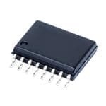
ICGOO电子元器件商城为您提供LT1054CDW由Texas Instruments设计生产,在icgoo商城现货销售,并且可以通过原厂、代理商等渠道进行代购。 LT1054CDW价格参考¥6.55-¥13.30。Texas InstrumentsLT1054CDW封装/规格:PMIC - 稳压器 - DC DC 开关稳压器, 可调(固定) 充电泵 开关稳压器 IC 正或负 3.5V(-Vin,2Vin) 1 输出 100mA 16-SOIC(0.295",7.50mm 宽)。您可以下载LT1054CDW参考资料、Datasheet数据手册功能说明书,资料中有LT1054CDW 详细功能的应用电路图电压和使用方法及教程。
LT1054CDW 是一款由 Texas Instruments(德州仪器)生产的 DC-DC 开关稳压器,属于 PMIC(电源管理集成电路)类别。该器件主要用于升压、降压和极性转换等应用场合,能够为各种电子设备提供稳定的电源输出。以下是 LT1054CDW 的主要应用场景:

 1. 电池供电设备
   - LT1054CDW 常用于便携式电池供电设备中,例如手持设备、无线通信装置、传感器模块等。它可以通过电荷泵技术将单节电池电压(如 1.5V 或 3V)转换为所需的稳定输出电压(如 ±6V),从而延长电池寿命并确保设备正常运行。

 2. 低功耗系统
   - 在低功耗设计中,LT1054CDW 可以高效地将输入电压转换为适合负载的输出电压。其内置的电荷泵结构能够在较低电流需求下实现高效率,适用于微控制器、传感器和其他低功耗组件的供电。

 3. 双极性电源供应
   - 该芯片支持生成正负对称的双极性电源(如 +5V 和 -5V),非常适合需要双电源供电的应用场景,例如运算放大器、模拟电路、音频处理电路和数据采集系统。

 4. 汽车电子
   - 在汽车电子领域,LT1054CDW 可用于为车载电子设备提供稳定的电源,例如仪表盘显示、娱乐系统和传感器接口。其宽泛的工作电压范围(1.5V 至 12V)使其能够适应汽车电池电压的变化。

 5. 工业控制
   - 工业自动化设备中常需要稳定的直流电源,LT1054CDW 可用于为 PLC(可编程逻辑控制器)、继电器驱动器和传感器接口提供可靠电源。其紧凑的设计和高效率特性特别适合空间受限的工业环境。

 6. 医疗设备
   - 在医疗设备中,例如便携式健康监测仪或诊断工具,LT1054CDW 能够提供精确且稳定的电源,确保测量结果的准确性。同时,其低噪声特性有助于减少对敏感信号的影响。

 7. 通信设备
   - 在无线通信模块和射频电路中,LT1054CDW 可以为发射器、接收器和信号处理单元提供稳定的电源支持。其高效的转换能力有助于降低功耗,延长设备工作时间。

总之,LT1054CDW 凭借其简单的设计、高效率和灵活性,广泛应用于各类需要稳定直流电源的场景,尤其是在低功耗、小型化和高可靠性要求的环境中表现优异。
| 参数 | 数值 |
| 产品目录 | 集成电路 (IC)半导体 |
| 描述 | IC REG SWITCHED CAP -5V 16SOIC稳压器—开关式稳压器 Bipolar Regulated V |
| 产品分类 | |
| 品牌 | Texas Instruments |
| 产品手册 | |
| 产品图片 |
|
| rohs | 符合RoHS无铅 / 符合限制有害物质指令(RoHS)规范要求 |
| 产品系列 | 电源管理 IC,稳压器—开关式稳压器,Texas Instruments LT1054CDW- |
| 数据手册 | |
| 产品型号 | LT1054CDW |
| PWM类型 | - |
| 产品目录页面 | |
| 产品种类 | 稳压器—开关式稳压器 |
| 供应商器件封装 | 16-SOIC |
| 其它名称 | 296-9590-5 |
| 包装 | 管件 |
| 单位重量 | 420.400 mg |
| 同步整流器 | 无 |
| 商标 | Texas Instruments |
| 安装类型 | 表面贴装 |
| 安装风格 | SMD/SMT |
| 宽度 | 7.52 mm |
| 封装 | Tube |
| 封装/外壳 | 16-SOIC(0.295",7.50mm 宽) |
| 封装/箱体 | SOIC-16 Wide |
| 工作温度 | 0°C ~ 70°C |
| 工作温度范围 | 0 C to + 70 C |
| 工厂包装数量 | 40 |
| 开关频率 | 25 kHz |
| 拓扑结构 | Buck-Boost |
| 最大工作温度 | + 70 C |
| 最大输入电压 | 15 V |
| 最小工作温度 | 0 C |
| 最小输入电压 | 3.5 V |
| 标准包装 | 40 |
| 电压-输入 | 3.5 V ~ 15 V |
| 电压-输出 | -5V |
| 电流-输出 | 100mA |
| 电源电压-最小 | 3.5 V |
| 类型 | 切换式电容器(充电泵) |
| 系列 | LT1054 |
| 输入电压 | 3.5 V to 15 V |
| 输出数 | 1 |
| 输出电压 | - 5 V |
| 输出电流 | 100 mA |
| 输出类型 | 固定 |
| 频率-开关 | 25kHz |

.jpg)


- 商务部:美国ITC正式对集成电路等产品启动337调查
- 曝三星4nm工艺存在良率问题 高通将骁龙8 Gen1或转产台积电
- 太阳诱电将投资9.5亿元在常州建新厂生产MLCC 预计2023年完工
- 英特尔发布欧洲新工厂建设计划 深化IDM 2.0 战略
- 台积电先进制程称霸业界 有大客户加持明年业绩稳了
- 达到5530亿美元!SIA预计今年全球半导体销售额将创下新高
- 英特尔拟将自动驾驶子公司Mobileye上市 估值或超500亿美元
- 三星加码芯片和SET,合并消费电子和移动部门,撤换高东真等 CEO
- 三星电子宣布重大人事变动 还合并消费电子和移动部门
- 海关总署:前11个月进口集成电路产品价值2.52万亿元 增长14.8%


PDF Datasheet 数据手册内容提取
Product Sample & Technical Tools & Support & Folder Buy Documents Software Community LT1054 SLVS033G–FEBRUARY1990–REVISEDJULY2015 LT1054 Switched-Capacitor Voltage Converters With Regulators 1 Features 3 Description • OutputCurrent,100mA The LT1054 device is a bipolar, switched-capacitor 1 voltage converter with regulator. It provides higher • LowLoss,1.1Vat100mA output current and significantly lower voltage losses • OperatingRange,3.5Vto15V than previously available converters. An adaptive- • ReferenceandErrorAmplifierforRegulation switch drive scheme optimizes efficiency over a wide rangeofoutputcurrents. • ExternalShutdown • ExternalOscillatorSynchronization Total voltage drop at 100-mA output current typically is 1.1 V. This applies to the full supply-voltage range • DevicesCanBeParalleled of 3.5 V to 15 V. Quiescent current typically is 2.5 • Pin-to-PinCompatibleWiththeLTC1044/7660 mA. 2 Applications The LT1054 also provides regulation, a feature previously not available in switched-capacitor voltage • IndustrialCommunications(RS232) converters. By adding an external resistive divider, a • DataAcquisitionSupply regulated output can be obtained. This output is regulated against changes in both input voltage and • VoltageInverters output current. The LT1054 can also shut down by • VoltageRegulators grounding the feedback terminal. Supply current in • NegativeVoltageDoublers shutdowntypicallyis100μA. • PositiveVoltageDoublers The internal oscillator of the LT1054 runs at a nominal frequency of 25 kHz. The oscillator terminal can be used to adjust the switching frequency or to externallysynchronizetheLT1054. The LT1054C is characterized for operation over a free-air temperature range of 0°C to 70°C. The LT1054I is characterized for operation over a free-air temperaturerangeof −40°Cto85°C. DeviceInformation(1) PARTNUMBER PACKAGE BODYSIZE(NOM) PDIP(8) 9.50mm×6.35mm LT1054 SOIC(16) 10.30mm×10.30mm (1) For all available packages, see the orderable addendum at theendofthedatasheet. BasicVoltageInverter 1 8 FB/SD VCC VIN + 2μF 2 7 CAP+ OSC LT1054 + 3 6 10μF GND VREF 4 5 CAP− VOUT −VOUT 100μF + 1 An IMPORTANT NOTICE at the end of this data sheet addresses availability, warranty, changes, use in safety-critical applications, intellectualpropertymattersandotherimportantdisclaimers.PRODUCTIONDATA.
LT1054 SLVS033G–FEBRUARY1990–REVISEDJULY2015 www.ti.com Table of Contents 1 Features.................................................................. 1 7.4 DeviceFunctionalModes........................................11 2 Applications........................................................... 1 8 ApplicationandImplementation........................ 13 3 Description............................................................. 1 8.1 ApplicationInformation ..........................................13 4 RevisionHistory..................................................... 2 8.2 TypicalApplication .................................................13 8.3 SystemExamples...................................................16 5 PinConfigurationandFunctions......................... 3 9 PowerSupplyRecommendations...................... 23 6 Specifications......................................................... 4 10 Layout................................................................... 24 6.1 AbsoluteMaximumRatings......................................4 6.2 ESDRatings ............................................................4 10.1 LayoutGuidelines.................................................24 6.3 RecommendedOperatingConditions.......................4 10.2 LayoutExample....................................................24 6.4 ThermalInformation .................................................4 11 DeviceandDocumentationSupport................. 25 6.5 ElectricalCharacteristics...........................................5 11.1 CommunityResources..........................................25 6.6 TypicalCharacteristics..............................................6 11.2 Trademarks...........................................................25 7 DetailedDescription.............................................. 9 11.3 ElectrostaticDischargeCaution............................25 7.1 Overview...................................................................9 11.4 Glossary................................................................25 7.2 FunctionalBlockDiagram.........................................9 12 Mechanical,Packaging,andOrderable Information........................................................... 25 7.3 FeatureDescription...................................................9 4 Revision History NOTE:Pagenumbersforpreviousrevisionsmaydifferfrompagenumbersinthecurrentversion. ChangesfromRevisionF(November2004)toRevisionG Page • AddedESDRatingstable,FeatureDescriptionsection,DeviceFunctionalModes,ApplicationandImplementation section,PowerSupplyRecommendationssection,Layoutsection,DeviceandDocumentationSupportsection,and Mechanical,Packaging,andOrderableInformationsection. ................................................................................................ 1 2 SubmitDocumentationFeedback Copyright©1990–2015,TexasInstrumentsIncorporated ProductFolderLinks:LT1054
LT1054 www.ti.com SLVS033G–FEBRUARY1990–REVISEDJULY2015 5 Pin Configuration and Functions PPackage 8-PinPDIP TopView FB/SD 1 8 VCC CAP+ 2 7 OSC GND 3 6 VREF CAP− 4 5 VOUT DWPackage 16-PinSOIC TopView NC 1 16 NC NC 2 15 NC FB/SD 3 14 VCC CAP+ 4 13 OSC GND 5 12 VREF CAP− 6 11 VOUT NC 7 10 NC NC 8 9 NC NC−No internal connection PinFunctions PIN I/O DESCRIPTION NAME PDIP SOIC FB/SD 1 3 Input ShutdownforlowIqoperationorerrorampinputforregulation CAP+ 2 4 Input PositivesideofCIN GND 3 5 — Ground CAP- 4 6 Input NegativesideofCIN V 5 11 Output Regulatedoutputvoltage OUT V 6 12 Output InternalReferenceVoltage REF OSC 7 13 Input Oscillatorcontrolpin V 8 14 — Supplypin CC 1,2,7,8,9, NC — — Noconnect(nointernalconnection) 10,15,16 Copyright©1990–2015,TexasInstrumentsIncorporated SubmitDocumentationFeedback 3 ProductFolderLinks:LT1054
LT1054 SLVS033G–FEBRUARY1990–REVISEDJULY2015 www.ti.com 6 Specifications 6.1 Absolute Maximum Ratings overoperatingfree-airtemperaturerange(unlessotherwisenoted)(1) MIN MAX UNIT V Supplyvoltage(2) 16 V CC FB/SD 0 V V CC V Inputvoltage I OSC 0 V V ref LT1054C 125 °C T Junctiontemperature(3) J LT1054I 135 °C T Storagetemperature –55 150 °C stg (1) StressesbeyondthoselistedunderAbsoluteMaximumRatingsmaycausepermanentdamagetothedevice.Thesearestressratings only,whichdonotimplyfunctionaloperationofthedeviceattheseoranyotherconditionsbeyondthoseindicatedunderRecommended OperatingConditions.Exposuretoabsolute-maximum-ratedconditionsforextendedperiodsmayaffectdevicereliability. (2) Theabsolutemaximumsupply-voltageratingof16Visforunregulatedcircuits.Forregulation-modecircuitswithV ≤15V,this OUT ratingmaybeincreasedto20V. (3) Thedevicesarefunctionaluptotheabsolutemaximumjunctiontemperature. 6.2 ESD Ratings VALUE UNIT Electrostatic Humanbodymodel(HBM),perANSI/ESDA/JEDECJS-001(1) ±500 V V (ESD) discharge Charged-devicemodel(CDM),perJEDECspecificationJESD22-C101(2) ±3500 (1) JEDECdocumentJEP155statesthat500-VHBMallowssafemanufacturingwithastandardESDcontrolprocess. (2) JEDECdocumentJEP157statesthat250-VCDMallowssafemanufacturingwithastandardESDcontrolprocess. 6.3 Recommended Operating Conditions overoperatingfree-airtemperaturerange(unlessotherwisenoted) MIN MAX UNIT V Supplyvoltage 3.5 15 V CC Operatingfree-air LT1054C 0 70 T °C A temperaturerange LT1054I –40 85 6.4 Thermal Information LT1054 THERMALMETRIC(1) P(PDIP) DW(SOIC) UNIT 8PINS 16PINS R Junction-to-ambientthermalresistance 85 57 °C/W θJA (1) Formoreinformationabouttraditionalandnewthermalmetrics,seetheSemiconductorandICPackageThermalMetricsapplication report,SPRA953. 4 SubmitDocumentationFeedback Copyright©1990–2015,TexasInstrumentsIncorporated ProductFolderLinks:LT1054
LT1054 www.ti.com SLVS033G–FEBRUARY1990–REVISEDJULY2015 6.5 Electrical Characteristics overrecommendedoperatingfree-airtemperaturerange(unlessotherwisenoted) LT1054C,LT1054I PARAMETER TESTCONDITIONS T (1) UNIT A MIN TYP(2) MAX V Regulatedoutputvoltage V =7V,T =25°C,R =500Ω (3) 25°C −4.7 −5 −5.2 V O CC J L Inputregulation V =7Vto12V,R =500Ω(3) Fullrange 5 25 mV CC L Outputregulation V =7V,R =100Ωto500Ω(3) Fullrange 10 50 mV CC L Voltageloss, IO=10mA 0.35 0.55 C =C =100-μFtantalum Fullrange V VCC−|VO| (4) I O IO=100mA 1.1 1.6 Outputresistance ΔI =10mAto100mA See (5) Fullrange 10 15 Ω O Oscillatorfrequency V =3.5Vto15V Fullrange 15 25 35 kHz CC 25°C 2.35 2.5 2.65 V Referencevoltage I =60μA V ref (REF) Fullrange 2.25 2.75 Maximumswitchcurrent 25°C 300 4 mA V =3.5V 2.5 5 CC I Supplycurrent I =0 Fullrange mA CC O V =15V 3 200 CC Supplycurrentin V =0V Fullrange 100 μA shutdown (FB/SD) (1) Fullrangeis0°Cto70°CfortheLT1054Cand−40°Cto85°CfortheLT1054I. (2) AlltypicalvaluesareatT =25°C. A (3) Allregulationspecificationsareforadeviceconnectedasapositive-to-negativeconverter/regulatorwithR1=20kΩ,R2=102.5kΩ, externalcapacitorC =10μF(tantalum),externalcapacitorC =100μF(tantalum)andC1=0.002μF(see). IN OUT (4) Forvoltage-losstests,thedeviceisconnectedasavoltageinverter,withterminals1,6,and7unconnected.Thevoltagelossesmaybe higherinotherconfigurations.C andC areexternalcapacitors. IN OUT (5) Outputresistanceisdefinedastheslopeofthecurve(ΔV versusΔI )foroutputcurrentsof10mAto100mA.Thisrepresentsthe O O linearportionofthecurve.Theincrementalslopeofthecurveishigheratcurrentslessthan10mAduetothecharacteristicsofthe switchtransistors. Copyright©1990–2015,TexasInstrumentsIncorporated SubmitDocumentationFeedback 5 ProductFolderLinks:LT1054
LT1054 SLVS033G–FEBRUARY1990–REVISEDJULY2015 www.ti.com 6.6 Typical Characteristics Dataathighandlowtemperaturesareapplicableonlywithintherecommendedoperatingfree-airtemperaturerange. Table1.TableofGraphs FIGURE Shutdownthresholdvoltage vsFree-airtemperature Figure1 Supplycurrent vsInputvoltage Figure2 Oscillatorfrequency vsFree-airtemperature Figure3 Supplycurrentinshutdown vsInputvoltage Figure4 Averagesupplycurrent vsOutputcurrent Figure5 Outputvoltageloss vsInputcapacitance Figure6 Outputvoltageloss vsOscillatorfrequency(10µF) Figure7 Outputvoltageloss vsOscillatorfrequency(100µF) Figure8 Regulatedoutputvoltage vsFree-airtemperature Figure9 Referencevoltagechange vsFree-airtemperature Figure10 Voltageloss vsOutputcurrent Figure17 0.6 5 IO= 0 V 0.5 − 4 e A g m a Volt 0.4 V(FB/SD) nt− old urre 3 esh 0.3 y C hr pl T p wn 0.2 Su 2 o − d C ut C h I S 0.1 1 0 0 −50 −25 0 25 50 75 100 0 5 10 15 TA−Free-AirTemperature−°C VCC−InputVoltage−V Figure1.ShutdownThresholdVoltagevsFree-Air Figure2.SupplyCurrentvsInputVoltage Temperature 6 SubmitDocumentationFeedback Copyright©1990–2015,TexasInstrumentsIncorporated ProductFolderLinks:LT1054
LT1054 www.ti.com SLVS033G–FEBRUARY1990–REVISEDJULY2015 35 120 33 A 100 31 μ ncy−kHz 2279 VCC=15V utdown− 80 V(FB/SD) = 0 e h u S Oscillator Freq 222351 VCC=3.5V ply Current in 6400 p 19 Su 20 17 15 0 −50 −25 0 25 50 75 100 0 5 10 15 TA−Free-AirTemperature−°C VCC−InputVoltage−V Figure3.OscillatorFrequencyvsFree-airTemperature Figure4.SupplyCurrentinShutdownvsInputVoltage 140 1.4 120 1.2 A IO= 100 mA m − 100 V 1.0 Supply Current 8600 VoltageLoss− 00..86 IO= 50 mA verage 40 Output 0.4 IO= 10 mA A Inverter Configuration 20 0.2 COUT= 100-μFTantalum fOSC=25kHz 0 0 0 20 40 60 80 100 0 10 20 30 40 50 60 70 80 90 100 IO−Output Current−mA Input Capacitance−μF Figure5.AverageSupplyCurrentvsOutputCurrent Figure6.OutputVoltageLossvsInputCapacitance 2.5 2.5 Inverter Configuration Inverter Configuration 2.25 CIN= 10-μFTantalum 2.25 CIN= 100-μFTantalum COUT= 100-μFTantalum COUT= 100-μFTantalum 2 2 V V 1.75 − 1.75 − s oss 1.5 Los 1.5 oltageL 1.25 IO=100mA Voltage 1.25 IO= 100 mA utputV 0.715 IO= 50 mA Output 0.715 IO= 50 mA O 0.5 IO= 10 mA 0.5 IO= 10 mA 0.25 0.25 0 0 1 10 100 1 10 100 Oscillator Frequency−kHz Oscillator Frequency−kHz Figure7.OutputVoltageLossvsOscillatorFrequency Figure8.OutputVoltageLossvsOscillatorFrequency Copyright©1990–2015,TexasInstrumentsIncorporated SubmitDocumentationFeedback 7 ProductFolderLinks:LT1054
LT1054 SLVS033G–FEBRUARY1990–REVISEDJULY2015 www.ti.com −4.7 100 −4.8 V 80 V m Voltage− −4−.59 hange− 4600 dOutput −−151..16 Voltage C 200 Regulate −1−11.82 eference −−2400 VREFat 0 = 2.500 V − R O − V −12.2 ef −60 Vr −12.4 ∆ −80 −12.6 −100 −50 −25 0 25 50 75 100 −50 −25 0 25 50 75 100 125 TA−Free-AirTemperature−°C TA−Free-AirTemperature−°C Figure9.RegulatedOutputVoltagevsFree-airTemperature Figure10.ReferenceVoltageChangevsFree-air Temperature 8 SubmitDocumentationFeedback Copyright©1990–2015,TexasInstrumentsIncorporated ProductFolderLinks:LT1054
LT1054 www.ti.com SLVS033G–FEBRUARY1990–REVISEDJULY2015 7 Detailed Description 7.1 Overview LT1054 is a "negative voltage generator" or "negative charge pump" that will output a negative voltage that is proportional to the input voltage (or V ). With proper supply voltage, V will regulate to an unregulated V CC OUT OUT that is approximately –V (reduced by a small voltage loss). If a lower absolute voltage is desired, V can be CC OUT regulatedtothatvaluewhenproperfeedbackresistorsareapplied. LT1054 regulates up to 100mA with minimal loss and has a shutdown mode that makes this part optimal across awiderangeofapplications. 7.2 Functional Block Diagram V V REF CC 6 8 2.5V Ref R Drive 2 + CAP+ 1 FB/SD 7 − Q CIN† OSC OSC 4 Q CAP− Drive R Drive 3 GND COUT† 5 VOUT Drive †External capacitors PinnumbersshownareforthePpackage. 7.3 Feature Description 7.3.1 ReferenceandErrorAmplifierforRegulation Thefeedback/shutdown(FB/SD)terminalhastwofunctions.PullingFB/SDbelowtheshutdownthreshold(≈ 0.45 V) puts the device into shutdown. In shutdown, the reference/regulator is turned off and switching stops. The switches are set such that both C and C are discharged through the output load. Quiescent current in IN OUT shutdown drops to approximately 100 µA. Any open-collector gate can be used to put the LT1054 into shutdown. For normal (unregulated) operation, the device will restart when the external gate is shut off. In LT1054 circuits that use the regulation feature, the external resistor divider can provide enough pulldown to keep the device in shutdown until the output capacitor (C ) has fully discharged. For most applications, where the LT1054 is run OUT intermittently, this does not present a problem because the discharge time of the output capacitor is short compared to the off time of the device. In applications where the device has to start up before the output capacitor (C ) has fully discharged, a restart pulse must be applied to FB/SD of the LT1054. Using the circuit OUT shown in Figure 11, the restart signal can be either a pulse (t > 100 µs) or a logic high. Diode coupling the p restart signal into FB/SD allows the output voltage to rise and regulate without overshoot. The resistor divider R3/R4showninFigure11shouldbechosentoprovideasignallevelatFB/SDof0.7−1.1V. FB/SD also is the inverting input of the LT1054 error amplifier and, as such, can be used to obtain a regulated outputvoltage. Copyright©1990–2015,TexasInstrumentsIncorporated SubmitDocumentationFeedback 9 ProductFolderLinks:LT1054
LT1054 SLVS033G–FEBRUARY1990–REVISEDJULY2015 www.ti.com Feature Description (continued) R3 VIN 2.2(cid:3)μF 1 8 + FB/SD VCC 2 7 CAP+ OSC R4 CIN + 3 LT1054 6 R1 10-μF GND VREF Tantalum 4 5 R2 CAP− VOUT Restart Shutdown For example: To get VO=−5V,referencedtothegroundterminaloftheLT1054 VOUT C1 æ ö æ ö R2=R1çèçççVR2EFV-OU4T0mV+1÷ø÷÷÷=20kWçèççç2.52V--54V0mV+1÷ø÷÷÷=102.6kW † C1Ta0On0U-tTμalFum Where: R1=20kΩ VREF=2.5VNominal † Choose the closest 1% value. Figure11. BasicRegulationConfiguration 7.3.2 ExternalOscillatorSynchronization This pin can be used to raise or lower the oscillator frequency or to synchronize the device to an external clock. Internally Pin 7 is connected to the oscillator timing capacitor (Ct ≈ 150pF) which is alternately charged and discharged by current sources of ±7µA so that the duty cycle is ≈50%. The LT1054 oscillator is designed to run in the frequency band where switching losses are minimized. However the frequency can be raised, lowered, or synchronizedtoanexternalsystemclockifnecessary. 1 8 C2 FB/SD V V CC IN 2 7 CAP+ OSC LT1054 + 3 6 GND V REF C1 4 5 CAP− V OUT Figure12. External-ClockSystem The frequency can be lowered by adding an external capacitor (C1, Figure 12) from Pin 7 to ground. This will increase the charge and discharge times which lowers the oscillator frequency. The frequency can be increased by adding an external capacitor (C2, Figure 12, in the range of 5pF to 20pF) from Pin 2 to Pin 7. This capacitor will couple charge into CT at the switch transitions, which will shorten the charge and discharge time, raising the oscillator frequency. Synchronization can be accomplished by adding an external resistive pull-up from Pin 7 to 10 SubmitDocumentationFeedback Copyright©1990–2015,TexasInstrumentsIncorporated ProductFolderLinks:LT1054
LT1054 www.ti.com SLVS033G–FEBRUARY1990–REVISEDJULY2015 Feature Description (continued) the reference pin (Pin 6). A 20k pull-up is recommended. An open collector gate or an NPN transistor can then be used to drive the oscillator pin at the external clock frequency as shown in Figure 12. Pulling up Pin 7 to an external voltage is not recommended. For circuits that require both frequency synchronization and regulation, an external reference can be used as the reference point for the top of the R1/R2 divider allowing Pin 6 to be used asapulluppointforPin7. 7.3.3 OutputCurrentandVoltageLoss The functional block diagram shows that the maximum regulated output voltage is limited by the supply voltage. For the basic configuration, |V | referenced to the ground terminal of the LT1054 must be less than the total of OUT the supply voltage minus the voltage loss due to the switches. The voltage loss versus output current due to the switchescanbefoundinthetypicalperformancecurves.Otherconfigurations,suchasthenegativedoubler,can providehighervoltagesatreducedoutputcurrents. 7.3.4 ReferenceVoltage Reference Output. This pin provides a 2.5V reference point for use in LT1054-based regulator circuits. The temperature coefficient of the reference voltage has been adjusted so that the temperature coefficient of the regulated output voltage is close to zero. This requires the reference output to have a positive temperature coefficient as can be seen in the typical performance curves. This nonzero drift is necessary to offset a drift term inherent in the internal reference divider and comparator network tied to the feedback pin. The overall result of thesedrifttermsisaregulatedoutputwhichhasaslight positive temperature coefficient at output voltages below 5V and a slight negative TC at output voltages above 5V. Reference output current should be limited, for regulator feedback networks, to approximately 60µA. The reference pin will draw ≈100µA when shorted to ground and will not affect the internal reference/regulator, so that this pin can also be used as a pull-up for LT1054circuitsthatrequiresynchronization. 7.4 Device Functional Modes 7.4.1 MainOperation A review of a basic switched-capacitor building block is helpful in understanding the operation of the LT1054. When the switch shown in Figure 13 is in the left position, capacitor C1 charges to the voltage at V1. The total charge on C1 is q1 = C1*V1. When the switch is moved to the right, C1 is discharged to the voltage at V2. After this discharge time, the charge on C1 is q2 = C1*V2. The charge has been transferred from the source V1 to the outputV2.TheamountofchargetransferredisshowninEquation1. Δq=q1–q2=C1(V1–V2) (1) If the switch is cycled f times per second, the charge transfer per unit time (that is, current) is as shown in Equation2. I=f×L\q=f×C1(1–V2) (2) To obtain an equivalent resistance for a switched-capacitor network, this equation can be rewritten in terms of voltageandimpedanceequivalenceasshowninEquation3. V1-V2 V1-V2 I= = (1/fC1) R EQUIV (3) V1 V2 f R L C1 C2 Figure13. Switched-CapacitorBuildingBlock Copyright©1990–2015,TexasInstrumentsIncorporated SubmitDocumentationFeedback 11 ProductFolderLinks:LT1054
LT1054 SLVS033G–FEBRUARY1990–REVISEDJULY2015 www.ti.com Device Functional Modes (continued) A new variable, R , is defined as R = 1 / (f × C1). The equivalent circuit for the switched-capacitor EQUIV EQUIV network is shown in Figure 14. The LT1054 has the same switching action as the basic switched-capacitor building block. Even though this simplification does not include finite switch-on resistance and output-voltage ripple,itprovidesaninsightintohowthedeviceoperates. R EQUIV V1 V2 1 C2 RL R EQUIV fC1 Figure14. Switched-CapacitorEquivalentCircuit These simplified circuits explain voltage loss as a function of oscillator frequency (see Figure 7). As oscillator frequency is decreased, the output impedance eventually is dominated by the 1 / (f × C1) term, and voltage lossesrise. Voltage losses also rise as oscillator frequency increases. This is caused by internal switching losses that occur due to some finite charge being lost on each switching cycle. This charge loss per-unit-cycle, when multiplied by the switching frequency, becomes a current loss. At high frequency, this loss becomes significant and voltage lossesagainrise. The oscillator of the LT1054 is designed to operate in the frequency band where voltage losses are at a minimum. 7.4.2 Shutdown LT1054 can be put into a low quiescent current state by grounding the FB/SD pin. Once FB/SD is pulled low, currentbeingdrawnfromthesupplywillbeapproximately100 µA. 12 SubmitDocumentationFeedback Copyright©1990–2015,TexasInstrumentsIncorporated ProductFolderLinks:LT1054
LT1054 www.ti.com SLVS033G–FEBRUARY1990–REVISEDJULY2015 8 Application and Implementation NOTE Information in the following applications sections is not part of the TI component specification, and TI does not warrant its accuracy or completeness. TI’s customers are responsible for determining suitability of components for their purposes. Customers should validateandtesttheirdesignimplementationtoconfirmsystemfunctionality. 8.1 Application Information The negative voltage converting and regulating ability of the LT1054 make this device optimal across a wide range of applications. As it is a regulator, there are many general design considerations that must be taken into account. Below will describe what to consider for using this device as a basic voltage inverter/regulator. This is the most common application for the LT1054 and the fundamental building block for the applications shown in SystemExamples. 8.2 Typical Application 8 FB/SD VCC VIN + 2μF 2 7 CAP+ OSC R1 LT1054 + 3 6 20kΩ 10μF GND VREF 4 5 R2 CAP− V OUT V OUT 0.002μF + + 100μF æ ö ç V ÷ æ V ö R2=R1ç OUT +1÷=20kWç OUT +1÷ ççVREF -40mV ÷÷ çè1.21V ÷ø è 2 ø PinnumbersshownareforthePpackage. Figure15. BasicVoltageInverter/Regulator 8.2.1 DesignRequirements Forthisdesignexample,usetheparameterslistedinTable2astheinputparameters. Table2.DesignParameters DesignParameter ExampleValue InputVoltageRange 3.5Vto15V V -5V OUT I 100mA OUT Copyright©1990–2015,TexasInstrumentsIncorporated SubmitDocumentationFeedback 13 ProductFolderLinks:LT1054
LT1054 SLVS033G–FEBRUARY1990–REVISEDJULY2015 www.ti.com 8.2.2 DetailedDesignProcedure WhenusingLT1054asabasicvoltageinverter,determinethefollowing: • InputVoltage • DesiredoutputVoltage • DesiredRipple • PowerDissipation 8.2.2.1 OutputVoltageProgramming The error amplifier of the LT1054 drives the PNP switch to control the voltage across the input capacitor (C ), IN whichdeterminestheoutputvoltage.WhenthereferenceanderroramplifieroftheLT1054areused,anexternal resistive divider is all that is needed to set the regulated output voltage. shows the basic regulator configuration and the formula for calculating the appropriate resistor values. R1 should be 20 kΩ or greater because the referencecurrentislimitedto ±100μA.R2shouldbeintherangeof100kΩ to300kΩ. 8.2.2.2 CapacitorSelection While the exact values of C and C are noncritical, good-quality low-ESR capacitors, such as solid tantalum, IN OUT are necessary to minimize voltage losses at high currents. For C , the effect of the ESR of the capacitor is IN multiplied by four, because switch currents are approximately two times higher than output current. Losses occur on both the charge and discharge cycle, which means that a capacitor with 1 Ω of ESR for C has the same IN effect as increasing the output impedance of the LT1054 by 4 Ω. This represents a significant increase in the voltage losses. C alternately is charged and discharged at a current approximately equal to the output OUT current. The ESR of the capacitor causes a step function to occur in the output ripple at the switch transitions. This step function degrades the output regulation for changes in output load current and should be avoided. A technique used to gain both low ESR and reasonable cost is to parallel a smaller tantalum capacitor with a large aluminumelectrolyticcapacitor. FrequencycompensationisaccomplishedbyadjustingtheratioofC toC . IN OUT For best results, this ratio should be approximately 1:10. Capacitor C1, required for good load regulation, should be0.002μFforalloutputvoltages. 8.2.2.3 OutputRipple Thepeak-to-peakoutputrippleisdeterminedbytheoutputcapacitorandtheoutputcurrentvalues.Peak-to-peak outputrippleisapproximatedas: I DV = OUT 2fC OUT where • ΔV=peak-to-peakripple • f =oscillatorfrequency (4) OSC For output capacitors with significant ESR, a second term must be added to account for the voltage step at the switchtransitions.Thisstepisapproximatelyequalto: (2I )(ESRofC ) (5) OUT OUT 8.2.2.4 PowerDissipation The power dissipation of any LT1054 circuit must be limited so that the junction temperature of the device does not exceed the maximum junction-temperature ratings. The total power dissipation is calculated from two components–thepowerlossduetovoltagedropsintheswitches,andthepowerlossduetodrive-currentlosses. ThetotalpowerdissipatedbytheLT1054iscalculatedas: P=(V –V )I +(V )(I )(0.2) CC OUT OUT CC OUT where • bothV andV arereferencedtoground (6) CC OUT 14 SubmitDocumentationFeedback Copyright©1990–2015,TexasInstrumentsIncorporated ProductFolderLinks:LT1054
LT1054 www.ti.com SLVS033G–FEBRUARY1990–REVISEDJULY2015 The power dissipation is equivalent to that of a linear regulator. Limited power-handling capability of the LT1054 packages causes limited output-current requirements, or steps can be taken to dissipate power external to the LT1054 for large input or output differentials. This is accomplished by placing a resistor in series with C as IN shown in Figure 16. A portion of the input voltage is dropped across this resistor without affecting the output regulation. Since switch current is approximately 2.2 times the output current and the resistor causes a voltage dropwhenC isbothcharginganddischarging,theresistorchosenisasshown: IN V R = x x 4.4 I OUT where • V ≈V −[(LT1054voltageloss)(1.3)+|V |] X CC OUT • I =maximumrequiredoutputcurrent (7) OUT Thefactorof1.3allowssomeoperatingmarginfortheLT1054. When using a 12-V to −5-V converter at 100-mA output current, calculate the power dissipation without an externalresistor. P=(12 V-|-5 V|)(100 mA)+(12 V)(100 mA)(0.2) P=700 mW+240 mW =940 mW (8) V IN 1 8 FB/SD V CC Rx 2 7 CAP+ OSC LT1054 + 3 6 R1 C GND V IN REF 4 5 R2 CAP− V OUT V OUT C1 C OUT + PinnumbersshownareforthePpackage. Figure16. Power-Dissipation-LimitingResistorinSeriesWithCIN At R of 130°C/W for a commercial plastic device, a junction temperature rise of 122°C occurs. The device θJA exceeds the maximum junction temperature at an ambient temperature of 25°C. To calculate the power dissipationwithanexternalresistor(R ),determinehowmuchvoltagecanbedroppedacrossRX.Themaximum X voltagelossoftheLT1054inthestandardregulatorconfigurationat100mAoutputcurrentis1.6V. V =12V–[(1.6V)(1.3)+|–5V|]=4.9V (9) X and 4.9 V R = =11W x (4.4)(100 mA) (10) Copyright©1990–2015,TexasInstrumentsIncorporated SubmitDocumentationFeedback 15 ProductFolderLinks:LT1054
LT1054 SLVS033G–FEBRUARY1990–REVISEDJULY2015 www.ti.com The resistor reduces the power dissipated by the LT1054 by (4.9 V)(100 mA) = 490 mW. The total power dissipated by the LT1054 is equal to (940 mW − 490 mW) = 450 mW. The junction-temperature rise is 58°C. Although commercial devices are functional up to a junction temperature of 125°C, the specifications are tested to a junction temperature of 100°C. In this example, this means limiting the ambient temperature to 42°C. To allow higher ambient temperatures, the thermal resistance numbers for the LT1054 packages represent worst- case numbers, with no heat sinking and still air. Small clip-on heat sinks can be used to lower the thermal resistance of the LT1054 package. Airflow in some systems helps to lower the thermal resistance. Wide printed circuit board traces from the LT1054 leads help remove heat from the device. This is especially true for plastic packages. 8.2.3 ApplicationCurve 2 3.5 V≤VCC≤15 V 1.8 Ci= Co= 100μF 1.6 1.4 TJ= 125°C V − s 1.2 s o e L 1 TJ= 25°C g a olt 0.8 V 0.6 0.4 0.2 TJ=−55°C 0 0 10 20 30 40 50 60 70 80 90 100 Output Current−mA Figure17.VoltageLossvsOutputCurrent 8.3 System Examples 10V 1N4002 100 kΩ 1 FB/SD VCC 8 100-kΩ + Speed Control 5μF 2 7 CAP+ OSC LT1054 − + 10μF 3 6 + 1N5817 GND VREF + − 4 5 CAP− VOUT Tach Motor NOTE: Motor-TachisCanonCKT26-T5-3SAE. PinnumbersshownareforthePpackage. Figure18. Motor-SpeedServo 16 SubmitDocumentationFeedback Copyright©1990–2015,TexasInstrumentsIncorporated ProductFolderLinks:LT1054
LT1054 www.ti.com SLVS033G–FEBRUARY1990–REVISEDJULY2015 System Examples (continued) 1 8 FB/SD VCC + 2 7 VOUT CAP+ OSC + LT1054 − 10μF 3 6 VIN GND VREF QX 2μF + 4 5 CAP− VOUT RX 100μF + VIN=−3.5Vto−15V VOUT=2VIN+(LT1054VoltageLoss)+(QXSaturationVoltage) VIN PinnumbersshownareforthePpackage. Figure19. Negative-VoltageDoubler VIN 3.5Vto15V 1N4001 1N4001 + + + 100μF 10μF VOUT 1 8 FB/SD VCC + − 2 7 2μF CAP+ OSC LT1054 3 6 GND VREF VVIONU=T3≈.52VVINto−1(5VLV+2VDiode) 4 CAP− VOUT 5 VL=LT1054VoltageLoss PinnumbersshownareforthePpackage. Figure20. Positive-VoltageDoubler Copyright©1990–2015,TexasInstrumentsIncorporated SubmitDocumentationFeedback 17 ProductFolderLinks:LT1054
LT1054 SLVS033G–FEBRUARY1990–REVISEDJULY2015 www.ti.com System Examples (continued) VIN 3.5 V to 15 V + 2.2μF 1 8 1 8 FB/SD VCC FB/SD VCC HP5082-2810 2 CAP+ OSC 7 VOUT 2 CAP+ OSC 7 CAP+ of SET LT1054 #1 +10μF LT1054 #1 + 10μF LT1054 #2 3 6 3 6 + GND VREF GND VREF 20 kΩ 10μF R1 4 5 4 5 CAP− VOUT 40 kΩ + CAP− VOUT 10μF 10μF + 1N4002 + 0.002μF 1N4002 10μF + 1N4002 R2 1N4002 500kΩ VOUT IOUT≅100 mAMAX 1N4002 100μF + VIN= 3.5 V to 15 V VOUTMAX≈−2 VIN+[LT1054VoltageLoss+2(VDiode)] æ ö ç V ÷ æ V ö R2 = R1ç OUT +1÷ = R1ç OUT +1÷ çç VREF -40 mV ÷÷ çè1.21V ÷ø è 2 ø PinnumbersshownareforthePpackage. Figure21. 100-mARegulatingNegativeDoubler VI 3.5 V to 15 V 1N4001 1N4001 + + +VO 100μF + 10μF 1 8 − FB/SD VCC 2 7 CAP+ OSC LT1054 3 6 + 10μF GND VREF 100μF 4 CAP− VOUT 5 + + 1N4001 10μF 1N4001 − +VVI=O 3≈.52 VV INto− 1(5V VL+2VDiode)−VO≈−2VI+(VL+2VDiode) 1N4001 + 100μF −VO VL=LT1054VoltageLoss + PinnumbersshownareforthePpackage. Figure22. Dual-OutputVoltageDoubler 18 SubmitDocumentationFeedback Copyright©1990–2015,TexasInstrumentsIncorporated ProductFolderLinks:LT1054
LT1054 www.ti.com SLVS033G–FEBRUARY1990–REVISEDJULY2015 System Examples (continued) 5μF 12 V + 1 8 1 8 FB/SD V FB/SD V CC CC HP5082-2810 10Ω 2 7 1/2 W 2 7 CAP+ OSC CAP+ OSC R1 LT1054 #1 + LT1054 #2 10Ω 3 6 39.2 kΩ 10μF 3 6 1/2 W GND VREF 0.002μF GND VREF + 20 kΩ 4 5 R2 4 5 CAP− V CAP− V + OUT 200 kΩ OUT 10μF V =−5 V O I = 0-200 mA O 200μF æ ö + ç V ÷ æ V ö R2=R1ç OUT +1÷=R1ç OUT +1÷ V ç1.21V ÷ çç REF -40mV ÷÷ è ø è 2 ø PinnumbersshownareforthePpackage. Figure23. 5-Vto ±12-VConverter 5 V 10kΩ + InCpMuOt TST LLoowr 10 kΩ 2N2907 40Ω 10μF ZeroTrim for On 10 kΩ GainTrim 5 kΩ 0.022μF 8 2 100 kΩ 301 kΩ 5 kΩ 6 A2 1 MΩ − − 1 1/2 1/2 7 LT1013 3 100 kΩ 10 kΩ 5 LT1013 VOUT + 350Ω + A1 4 1μF 200 kΩ 1 8 FB/SD VCC 5 V 2 7 CAP+ OSC + 3 kΩ 10μF LT1054 #1 2N2222 3 6 GND VREF + 100-μF Tantalum Adjust Gain Trim For 3 V Out From 4 5 CAP− VOUT Full-ScaleBridgeOutputof24mV PinnumbersshownareforthePpackage. Figure24. Strain-GageBridgeSignalConditioner Copyright©1990–2015,TexasInstrumentsIncorporated SubmitDocumentationFeedback 19 ProductFolderLinks:LT1054
LT1054 SLVS033G–FEBRUARY1990–REVISEDJULY2015 www.ti.com System Examples (continued) VI 3.5Vto5.5V 1 8 20 kΩ FB/SD VCC 2 7 CAP+ OSC + LTC1044 1μF 3 6 1N914 GND VREF (All) 1 8 FB/SD VCC 4 CAP− VOUT 5 + 2 7 5μF R2 CAP+ OSC 125 kΩ R1 LT1054 + 3 6 20 kΩ 10μF GND VREF + 1μF + 4 CAP− VOUT 5 0.002μF R1225kΩ +100μF 3 kΩ VO − VI= 3.5 V to 5.5 V VO= 5 V 2N2219 IOMAX = 50 mA æ ö 1N914 1N5817 ç V ÷ æ V ö R2=R1ç OUT +1÷=R1ç OUT +1÷ V ç1.21V ÷ çç REF -40mV ÷÷ è ø è 2 ø PinnumbersshownareforthePpackage. Figure25. 3.5-Vto5-VRegulator 20 SubmitDocumentationFeedback Copyright©1990–2015,TexasInstrumentsIncorporated ProductFolderLinks:LT1054
LT1054 www.ti.com SLVS033G–FEBRUARY1990–REVISEDJULY2015 System Examples (continued) 5μF 12 V + 1 8 1 8 FB/SD V FB/SD V CC CC HP5082-2810 10Ω 2 7 1/2 W 2 7 CAP+ OSC CAP+ OSC R1 LT1054 #1 + LT1054 #2 10Ω 3 6 39.2 kΩ 10μF 3 6 1/2 W GND VREF 0.002μF GND VREF + 20 kΩ 4 5 R2 4 5 CAP− V CAP− V + OUT 200 kΩ OUT 10μF V =−5 V O I = 0-200 mA O 200μF æ ö + ç V ÷ æ V ö R2=R1ç OUT +1÷=R1ç OUT +1÷ V ç1.21V ÷ çç REF -40mV ÷÷ è ø è 2 ø PinnumbersshownareforthePpackage. Figure26. Regulating200-mA+12-Vto−5-VConverter 15 V 5μF + 11 20 kΩ 16 Digital AD558 Input 2.5 V LT1004-2.5 15 1 8 14 13 12 FB/SD VCC 2 7 CAP+ OSC 20 kΩ LT1054 + 3 6 10μF GND VREF 4 5 CAP− VOUT VO=−VI(Programmed) 100μF + PinnumbersshownareforthePpackage. Figure27. DigitallyProgrammableNegativeSupply Copyright©1990–2015,TexasInstrumentsIncorporated SubmitDocumentationFeedback 21 ProductFolderLinks:LT1054
LT1054 SLVS033G–FEBRUARY1990–REVISEDJULY2015 www.ti.com System Examples (continued) V =5V I 2(cid:3)μF + 50kΩ 1N5817 1 8 FB/SD V CC 1N5817 10μF VO + 2 7 8 V CAP+ OSC + LT1054 100μF 0.03μF 10 kΩ 10 kΩ 3 6 GND V 5.5 kΩ REF 5V 4 5 10 kΩ CAP− V OUT − 1/2 2.5 kΩ LT1013 + 0.1μF PinnumbersshownareforthePpackage. Figure28. PositiveDoublerWithRegulation(5-Vto8-VConverter) VI 3.5 V to 15 V 2(cid:3)μF 1 8 + FB/SD VCC 2 7 CAP+ OSC LT1054 R1 + 3 6 60 kΩ 10μF GND VREF 100μF 4 5 + CAP− VOUT R2 + + 1MΩ 0.002μF 10μF 1N4001 1N4001 −VO VI= 3.5 V to 15 V VOMAX≈2VIN+(VL+2VDiode) 100μF VL=LT1054VoltageLoss æ ö ç V ÷ æ V ö R2=R1ç OUT +1÷=R1ç OUT +1÷ ççVREF -40mV ÷÷ çè1.21V ÷ø è 2 ø PinnumbersshownareforthePpackage. Figure29. NegativeDoublerWithRegulator 22 SubmitDocumentationFeedback Copyright©1990–2015,TexasInstrumentsIncorporated ProductFolderLinks:LT1054
LT1054 www.ti.com SLVS033G–FEBRUARY1990–REVISEDJULY2015 9 Power Supply Recommendations TheLT1054alternatelychargesC totheinputvoltagewhenC isswitchedinparallelwiththeinputsupplyand IN IN then transfers charge to C when C is switched in parallel with C . Switching occurs at the oscillator OUT IN OUT frequency. During the time that C is charging, the peak supply current will be approximately equal to 2.2 times IN theoutputcurrent.DuringthetimethatC isdeliveringchargetoC thesupplycurrentdropstoapproximately IN OUT 0.2 times the output current. An input supply bypass capacitor will supply part of the peak input current drawn by the LT1054 and average out the current drawn from the supply. A minimum input supply bypass capacitor of 2µF, preferably tantalum or some other low ESR type is recommended. A larger capacitor may be desirable in some cases, for example, when the actual input supply is connected to the LT1054 through long leads, or when thepulsecurrentdrawnbytheLT1054mightaffectothercircuitrythroughsupplycoupling. In addition to being the output terminal, V is tied to the substrate of the device. Special care must be taken in OUT LT1054 circuits to avoid making V positive with respect to any of the other terminals. For circuits with the OUT output load connected from V to V or from some external positive supply voltage to V , an external CC OUT OUT transistor must be added (see Figure 30). This transistor prevents V from being pulled above GND during OUT startup. Any small general-purpose transistor such as a 2N2222 or a 2N2219 device can be used. Resistor R1 should be chosen to provide enough base drive to the external transistor so that it is saturated under nominal outputvoltageandmaximumoutputcurrentconditions. (V )b OUT R1£ I OUT (11) V IN 1 8 FB/SD V Load CC 2 7 VOUT CAP+ OSC R1 LT1054 + 3 6 C GND V IN REF 4 5 CAP− V OUT C OUT + Figure30. CircuitWithLoadConnectedfromV toV CC OUT Copyright©1990–2015,TexasInstrumentsIncorporated SubmitDocumentationFeedback 23 ProductFolderLinks:LT1054
LT1054 SLVS033G–FEBRUARY1990–REVISEDJULY2015 www.ti.com 10 Layout 10.1 Layout Guidelines • Try to run the feedback trace as far from the noisy power or clocking traces as possible. In the case that the OSC pin is not being used, as in Figure 31, the FB trace can be ran on a lower layer under the OSC pin. WhenOSCisbeingutilizedbyanoisyclockingsignal,itisrecommendedtoruntheFBtraceonalowerlayer throughtheVrefpin. – Keep the FB trace to be as direct as possible and somewhat thick. These two sometimes involve a trade- off,butkeepingitawayfromEMIandothernoisesourcesisthemorecriticalofthetwo. • Keep the external capacitor traces short, specifically on the CAP+ and CAP- nodes that have the fastest rise andfalltimes. • Make all of the power (high current) traces as short, direct, and thick as possible. It is good practice on a standardPCBboardtomakethetracesanabsoluteminimumof15mils(0.381mm)perAmpere. 10.2 Layout Example Ground 2.0 PF FB/SD 1 8 VCC Positive Supply CAP+ 2 7 OSC R1 Ground GND 3 6 VREF 10 PF &$3í 4 5 VOUT R2 0.002 PF 100 PF Ground Figure31. BasicInverter/RegulatorLayout 24 SubmitDocumentationFeedback Copyright©1990–2015,TexasInstrumentsIncorporated ProductFolderLinks:LT1054
LT1054 www.ti.com SLVS033G–FEBRUARY1990–REVISEDJULY2015 11 Device and Documentation Support 11.1 Community Resources The following links connect to TI community resources. Linked contents are provided "AS IS" by the respective contributors. They do not constitute TI specifications and do not necessarily reflect TI's views; see TI's Terms of Use. TIE2E™OnlineCommunity TI'sEngineer-to-Engineer(E2E)Community.Createdtofostercollaboration amongengineers.Ate2e.ti.com,youcanaskquestions,shareknowledge,exploreideasandhelp solveproblemswithfellowengineers. DesignSupport TI'sDesignSupport QuicklyfindhelpfulE2Eforumsalongwithdesignsupporttoolsand contactinformationfortechnicalsupport. 11.2 Trademarks E2EisatrademarkofTexasInstruments. Allothertrademarksarethepropertyoftheirrespectiveowners. 11.3 Electrostatic Discharge Caution Thesedeviceshavelimitedbuilt-inESDprotection.Theleadsshouldbeshortedtogetherorthedeviceplacedinconductivefoam duringstorageorhandlingtopreventelectrostaticdamagetotheMOSgates. 11.4 Glossary SLYZ022—TIGlossary. Thisglossarylistsandexplainsterms,acronyms,anddefinitions. 12 Mechanical, Packaging, and Orderable Information The following pages include mechanical, packaging, and orderable information. This information is the most current data available for the designated devices. This data is subject to change without notice and revision of thisdocument.Forbrowser-basedversionsofthisdatasheet,refertotheleft-handnavigation. Copyright©1990–2015,TexasInstrumentsIncorporated SubmitDocumentationFeedback 25 ProductFolderLinks:LT1054
PACKAGE OPTION ADDENDUM www.ti.com 6-Feb-2020 PACKAGING INFORMATION Orderable Device Status Package Type Package Pins Package Eco Plan Lead/Ball Finish MSL Peak Temp Op Temp (°C) Device Marking Samples (1) Drawing Qty (2) (6) (3) (4/5) LT1054CDW ACTIVE SOIC DW 16 40 Green (RoHS NIPDAU Level-1-260C-UNLIM 0 to 70 LT1054C & no Sb/Br) LT1054CDWG4 ACTIVE SOIC DW 16 40 Green (RoHS NIPDAU Level-1-260C-UNLIM 0 to 70 LT1054C & no Sb/Br) LT1054CDWR ACTIVE SOIC DW 16 2000 Green (RoHS NIPDAU Level-1-260C-UNLIM 0 to 70 LT1054C & no Sb/Br) LT1054CDWRE4 ACTIVE SOIC DW 16 2000 Green (RoHS NIPDAU Level-1-260C-UNLIM 0 to 70 LT1054C & no Sb/Br) LT1054CDWRG4 ACTIVE SOIC DW 16 2000 Green (RoHS NIPDAU Level-1-260C-UNLIM 0 to 70 LT1054C & no Sb/Br) LT1054CP ACTIVE PDIP P 8 50 Green (RoHS NIPDAU N / A for Pkg Type 0 to 70 LT1054CP & no Sb/Br) LT1054CPE4 ACTIVE PDIP P 8 50 Green (RoHS NIPDAU N / A for Pkg Type 0 to 70 LT1054CP & no Sb/Br) LT1054IDW ACTIVE SOIC DW 16 40 Green (RoHS NIPDAU Level-1-260C-UNLIM -40 to 85 LT1054I & no Sb/Br) LT1054IDWG4 ACTIVE SOIC DW 16 40 Green (RoHS NIPDAU Level-1-260C-UNLIM -40 to 85 LT1054I & no Sb/Br) LT1054IDWR ACTIVE SOIC DW 16 2000 Green (RoHS NIPDAU Level-1-260C-UNLIM -40 to 85 LT1054I & no Sb/Br) LT1054IP ACTIVE PDIP P 8 50 Green (RoHS NIPDAU N / A for Pkg Type -40 to 85 LT1054IP & no Sb/Br) LT1054IPE4 ACTIVE PDIP P 8 50 Green (RoHS NIPDAU N / A for Pkg Type -40 to 85 LT1054IP & no Sb/Br) (1) The marketing status values are defined as follows: ACTIVE: Product device recommended for new designs. LIFEBUY: TI has announced that the device will be discontinued, and a lifetime-buy period is in effect. NRND: Not recommended for new designs. Device is in production to support existing customers, but TI does not recommend using this part in a new design. PREVIEW: Device has been announced but is not in production. Samples may or may not be available. OBSOLETE: TI has discontinued the production of the device. (2) RoHS: TI defines "RoHS" to mean semiconductor products that are compliant with the current EU RoHS requirements for all 10 RoHS substances, including the requirement that RoHS substance do not exceed 0.1% by weight in homogeneous materials. Where designed to be soldered at high temperatures, "RoHS" products are suitable for use in specified lead-free processes. TI may reference these types of products as "Pb-Free". RoHS Exempt: TI defines "RoHS Exempt" to mean products that contain lead but are compliant with EU RoHS pursuant to a specific EU RoHS exemption. Addendum-Page 1
PACKAGE OPTION ADDENDUM www.ti.com 6-Feb-2020 Green: TI defines "Green" to mean the content of Chlorine (Cl) and Bromine (Br) based flame retardants meet JS709B low halogen requirements of <=1000ppm threshold. Antimony trioxide based flame retardants must also meet the <=1000ppm threshold requirement. (3) MSL, Peak Temp. - The Moisture Sensitivity Level rating according to the JEDEC industry standard classifications, and peak solder temperature. (4) There may be additional marking, which relates to the logo, the lot trace code information, or the environmental category on the device. (5) Multiple Device Markings will be inside parentheses. Only one Device Marking contained in parentheses and separated by a "~" will appear on a device. If a line is indented then it is a continuation of the previous line and the two combined represent the entire Device Marking for that device. (6) Lead/Ball Finish - Orderable Devices may have multiple material finish options. Finish options are separated by a vertical ruled line. Lead/Ball Finish values may wrap to two lines if the finish value exceeds the maximum column width. Important Information and Disclaimer:The information provided on this page represents TI's knowledge and belief as of the date that it is provided. TI bases its knowledge and belief on information provided by third parties, and makes no representation or warranty as to the accuracy of such information. Efforts are underway to better integrate information from third parties. TI has taken and continues to take reasonable steps to provide representative and accurate information but may not have conducted destructive testing or chemical analysis on incoming materials and chemicals. TI and TI suppliers consider certain information to be proprietary, and thus CAS numbers and other limited information may not be available for release. In no event shall TI's liability arising out of such information exceed the total purchase price of the TI part(s) at issue in this document sold by TI to Customer on an annual basis. Addendum-Page 2
PACKAGE MATERIALS INFORMATION www.ti.com 12-Feb-2019 TAPE AND REEL INFORMATION *Alldimensionsarenominal Device Package Package Pins SPQ Reel Reel A0 B0 K0 P1 W Pin1 Type Drawing Diameter Width (mm) (mm) (mm) (mm) (mm) Quadrant (mm) W1(mm) LT1054CDWR SOIC DW 16 2000 330.0 16.4 10.75 10.7 2.7 12.0 16.0 Q1 LT1054IDWR SOIC DW 16 2000 330.0 16.4 10.75 10.7 2.7 12.0 16.0 Q1 PackMaterials-Page1
PACKAGE MATERIALS INFORMATION www.ti.com 12-Feb-2019 *Alldimensionsarenominal Device PackageType PackageDrawing Pins SPQ Length(mm) Width(mm) Height(mm) LT1054CDWR SOIC DW 16 2000 350.0 350.0 43.0 LT1054IDWR SOIC DW 16 2000 350.0 350.0 43.0 PackMaterials-Page2
GENERIC PACKAGE VIEW DW 16 SOIC - 2.65 mm max height 7.5 x 10.3, 1.27 mm pitch SMALL OUTLINE INTEGRATED CIRCUIT This image is a representation of the package family, actual package may vary. Refer to the product data sheet for package details. 4224780/A www.ti.com
PACKAGE OUTLINE DW0016A SOIC - 2.65 mm max height SCALE 1.500 SOIC C 10.63 SEATING PLANE TYP 9.97 A PIN 1 ID 0.1 C AREA 14X 1.27 16 1 10.5 2X 10.1 8.89 NOTE 3 8 9 0.51 16X 0.31 7.6 B 7.4 0.25 C A B 2.65 MAX NOTE 4 0.33 TYP 0.10 SEE DETAIL A 0.25 GAGE PLANE 0.3 0 - 8 0.1 1.27 0.40 DETAIL A (1.4) TYPICAL 4220721/A 07/2016 NOTES: 1. All linear dimensions are in millimeters. Dimensions in parenthesis are for reference only. Dimensioning and tolerancing per ASME Y14.5M. 2. This drawing is subject to change without notice. 3. This dimension does not include mold flash, protrusions, or gate burrs. Mold flash, protrusions, or gate burrs shall not exceed 0.15 mm, per side. 4. This dimension does not include interlead flash. Interlead flash shall not exceed 0.25 mm, per side. 5. Reference JEDEC registration MS-013. www.ti.com
EXAMPLE BOARD LAYOUT DW0016A SOIC - 2.65 mm max height SOIC 16X (2) SEE SYMM DETAILS 1 16 16X (0.6) SYMM 14X (1.27) 8 9 R0.05 TYP (9.3) LAND PATTERN EXAMPLE SCALE:7X METAL SOLDER MASK SOLDER MASK METAL OPENING OPENING 0.07 MAX 0.07 MIN ALL AROUND ALL AROUND NON SOLDER MASK SOLDER MASK DEFINED DEFINED SOLDER MASK DETAILS 4220721/A 07/2016 NOTES: (continued) 6. Publication IPC-7351 may have alternate designs. 7. Solder mask tolerances between and around signal pads can vary based on board fabrication site. www.ti.com
EXAMPLE STENCIL DESIGN DW0016A SOIC - 2.65 mm max height SOIC 16X (2) SYMM 1 16 16X (0.6) SYMM 14X (1.27) 8 9 R0.05 TYP (9.3) SOLDER PASTE EXAMPLE BASED ON 0.125 mm THICK STENCIL SCALE:7X 4220721/A 07/2016 NOTES: (continued) 8. Laser cutting apertures with trapezoidal walls and rounded corners may offer better paste release. IPC-7525 may have alternate design recommendations. 9. Board assembly site may have different recommendations for stencil design. www.ti.com
None
IMPORTANTNOTICEANDDISCLAIMER TI PROVIDES TECHNICAL AND RELIABILITY DATA (INCLUDING DATASHEETS), DESIGN RESOURCES (INCLUDING REFERENCE DESIGNS), APPLICATION OR OTHER DESIGN ADVICE, WEB TOOLS, SAFETY INFORMATION, AND OTHER RESOURCES “AS IS” AND WITH ALL FAULTS, AND DISCLAIMS ALL WARRANTIES, EXPRESS AND IMPLIED, INCLUDING WITHOUT LIMITATION ANY IMPLIED WARRANTIES OF MERCHANTABILITY, FITNESS FOR A PARTICULAR PURPOSE OR NON-INFRINGEMENT OF THIRD PARTY INTELLECTUAL PROPERTY RIGHTS. These resources are intended for skilled developers designing with TI products. You are solely responsible for (1) selecting the appropriate TI products for your application, (2) designing, validating and testing your application, and (3) ensuring your application meets applicable standards, and any other safety, security, or other requirements. These resources are subject to change without notice. TI grants you permission to use these resources only for development of an application that uses the TI products described in the resource. Other reproduction and display of these resources is prohibited. No license is granted to any other TI intellectual property right or to any third party intellectual property right. TI disclaims responsibility for, and you will fully indemnify TI and its representatives against, any claims, damages, costs, losses, and liabilities arising out of your use of these resources. TI’s products are provided subject to TI’s Terms of Sale (www.ti.com/legal/termsofsale.html) or other applicable terms available either on ti.com or provided in conjunction with such TI products. TI’s provision of these resources does not expand or otherwise alter TI’s applicable warranties or warranty disclaimers for TI products. Mailing Address: Texas Instruments, Post Office Box 655303, Dallas, Texas 75265 Copyright © 2020, Texas Instruments Incorporated