ICGOO在线商城 > 集成电路(IC) > PMIC - 稳压器 - DC DC 开关稳压器 > LM2575S-5.0/NOPB

 Datasheet下载
- 型号: LM2575S-5.0/NOPB
- 制造商: Texas Instruments
- 库位|库存: xxxx|xxxx
- 要求:
| 数量阶梯 | 香港交货 | 国内含税 |
| +xxxx | $xxxx | ¥xxxx |
查看当月历史价格
查看今年历史价格
LM2575S-5.0/NOPB产品简介:
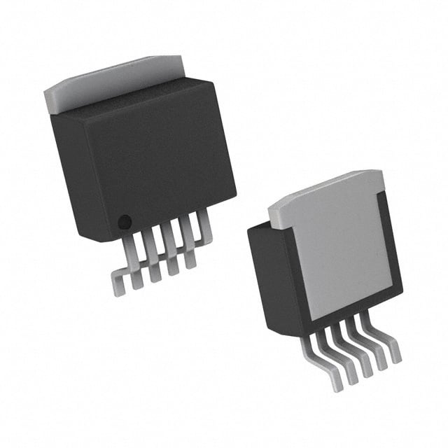
ICGOO电子元器件商城为您提供LM2575S-5.0/NOPB由Texas Instruments设计生产,在icgoo商城现货销售,并且可以通过原厂、代理商等渠道进行代购。 LM2575S-5.0/NOPB价格参考。Texas InstrumentsLM2575S-5.0/NOPB封装/规格:PMIC - 稳压器 - DC DC 开关稳压器, 固定 降压 开关稳压器 IC 正 5V 1 输出 1A TO-263-6,D²Pak(5 引线 + 接片),TO-263BA。您可以下载LM2575S-5.0/NOPB参考资料、Datasheet数据手册功能说明书,资料中有LM2575S-5.0/NOPB 详细功能的应用电路图电压和使用方法及教程。
LM2575S-5.0/NOPB 是由德州仪器 (Texas Instruments) 生产的一款 PMIC(电源管理集成电路),具体分类为 DC-DC 开关稳压器。该型号的稳压器具有高效、低纹波和高稳定性等特点,广泛应用于各种需要将较高电压转换为稳定 5V 输出的场景。

 应用场景:

1. 消费电子设备:
   - 便携式电子产品:如手机充电器、平板电脑适配器等。这些设备通常需要一个稳定的 5V 输出来为电池充电或为内部电路供电。
   - USB 充电器:LM2575S-5.0/NOPB 可以用于 USB 充电器中,提供稳定的 5V 输出,确保连接的设备能够安全快速地充电。

2. 工业控制:
   - 传感器模块:在工业自动化系统中,传感器模块通常需要一个稳定的 5V 电源来确保其正常工作。LM2575S-5.0/NOPB 可以将工业标准的 12V 或 24V 输入电压转换为所需的 5V 输出。
   - PLC(可编程逻辑控制器):PLC 需要稳定的电源供应来保证其内部处理器和输入输出模块的正常运行。LM2575S-5.0/NOPB 可以为 PLC 提供可靠的 5V 电源。

3. 通信设备:
   - 网络路由器和交换机:这些设备通常需要多个不同电压的电源轨,其中 5V 是常见的电源需求之一。LM2575S-5.0/NOPB 可以用于将主电源转换为 5V,为路由器或交换机中的微控制器和其他组件供电。
   - 无线模块:例如 Wi-Fi 模块、蓝牙模块等,这些模块通常需要 5V 的稳定电源来确保其无线通信功能的正常运行。

4. 汽车电子:
   - 车载娱乐系统:现代汽车中的娱乐系统(如导航仪、音响系统)通常需要 5V 电源来驱动其内部的处理器和接口电路。LM2575S-5.0/NOPB 可以从汽车电池提供的 12V 或 24V 电压中转换出稳定的 5V 输出。
   - 车载诊断系统 (OBD):OBD 设备通常需要 5V 电源来读取车辆的传感器数据并进行故障诊断。LM2575S-5.0/NOPB 可以为 OBD 设备提供稳定的电源支持。

总之,LM2575S-5.0/NOPB 凭借其高效的转换效率和稳定的输出特性,适用于多种需要 5V 稳定电源的应用场景,特别是在那些对电源质量要求较高的场合。
| 参数 | 数值 |
| 产品目录 | 集成电路 (IC)半导体 |
| 描述 | IC REG BUCK 5V 1A TO263-5稳压器—开关式稳压器 1A STEP-DOWN VLTG REG |
| 产品分类 | |
| 品牌 | Texas Instruments |
| 产品手册 | |
| 产品图片 |
|
| rohs | 符合RoHS含铅 / 不受限制有害物质指令(RoHS)规范要求限制 |
| 产品系列 | 电源管理 IC,稳压器—开关式稳压器,Texas Instruments LM2575S-5.0/NOPBSIMPLE SWITCHER® |
| 数据手册 | |
| 产品型号 | LM2575S-5.0/NOPB |
| PWM类型 | 电压模式 |
| 产品培训模块 | http://www.digikey.cn/PTM/IndividualPTM.page?site=cn&lang=zhs&ptm=30128 |
| 产品目录页面 | |
| 产品种类 | 稳压器—开关式稳压器 |
| 供应商器件封装 | DDPAK/TO-263-5 |
| 其它名称 | *LM2575S-5.0/NOPB |
| 制造商产品页 | http://www.ti.com/general/docs/suppproductinfo.tsp?distId=10&orderablePartNumber=LM2575S-5.0/NOPB |
| 包装 | 管件 |
| 同步整流器 | 无 |
| 商标 | Texas Instruments |
| 安装类型 | 表面贴装 |
| 安装风格 | SMD/SMT |
| 封装 | Tube |
| 封装/外壳 | TO-263-6,D²Pak(5 引线+接片),TO-263BA |
| 封装/箱体 | TO-263 |
| 工作温度 | -40°C ~ 125°C |
| 工作温度范围 | - 40 C to + 85 C |
| 工厂包装数量 | 45 |
| 开关频率 | 58 kHz |
| 最大工作温度 | + 125 C |
| 最大输入电压 | 40 V |
| 最小工作温度 | - 40 C |
| 最小输入电压 | 4 V |
| 标准包装 | 45 |
| 电压-输入 | 4 V ~ 40 V |
| 电压-输出 | 5V |
| 电流-输出 | 1A |
| 类型 | 降压(降压) |
| 系列 | LM2575-N |
| 输出数 | 1 |
| 输出电压 | 5 V |
| 输出电流 | 1 A |
| 输出端数量 | 1 Output |
| 输出类型 | 固定 |
| 频率-开关 | 52kHz |


- 商务部:美国ITC正式对集成电路等产品启动337调查
- 曝三星4nm工艺存在良率问题 高通将骁龙8 Gen1或转产台积电
- 太阳诱电将投资9.5亿元在常州建新厂生产MLCC 预计2023年完工
- 英特尔发布欧洲新工厂建设计划 深化IDM 2.0 战略
- 台积电先进制程称霸业界 有大客户加持明年业绩稳了
- 达到5530亿美元!SIA预计今年全球半导体销售额将创下新高
- 英特尔拟将自动驾驶子公司Mobileye上市 估值或超500亿美元
- 三星加码芯片和SET,合并消费电子和移动部门,撤换高东真等 CEO
- 三星电子宣布重大人事变动 还合并消费电子和移动部门
- 海关总署:前11个月进口集成电路产品价值2.52万亿元 增长14.8%


PDF Datasheet 数据手册内容提取
LM1575, LM2575-N, LM2575HV www.ti.com SNVS106E–MAY1999–REVISEDAPRIL2013 ® LM1575/LM2575/LM2575HV SIMPLE SWITCHER 1A Step-Down Voltage Regulator CheckforSamples:LM1575,LM2575-N,LM2575HV FEATURES DESCRIPTION 1 • 3.3V,5V,12V,15V,andAdjustableOutput The LM2575 series of regulators are monolithic 23 integrated circuits that provide all the active functions Versions for a step-down (buck) switching regulator, capable of • AdjustableVersionOutputVoltageRange, driving a 1A load with excellent line and load – 1.23Vto37V(57VforHVVersion)±4% regulation.Thesedevicesareavailableinfixedoutput MaxOver voltages of 3.3V, 5V, 12V, 15V, and an adjustable outputversion. – LineandLoadConditions • Specified1AOutputCurrent Requiring a minimum number of external components, these regulators are simple to use and • WideInputVoltageRange,40Vupto60Vfor include internal frequency compensation and a fixed- HVVersion frequencyoscillator. • RequiresOnly4ExternalComponents The LM2575 series offers a high-efficiency • 52kHzFixedFrequencyInternalOscillator replacement for popular three-terminal linear • TTLShutdownCapability,LowPowerStandby regulators. It substantially reduces the size of the Mode heat sink, and in many cases no heat sink is required. • HighEfficiency • UsesReadilyAvailableStandardInductors A standard series of inductors optimized for use with the LM2575 are available from several different • ThermalShutdownandCurrentLimit manufacturers. This feature greatly simplifies the Protection designofswitch-modepowersupplies. • P+ProductEnhancementTested Other features include a specified ±4% tolerance on output voltage within specified input voltages and APPLICATIONS output load conditions, and ±10% on the oscillator • SimpleHigh-EfficiencyStep-Down(Buck) frequency. External shutdown is included, featuring Regulator 50 μA (typical) standby current. The output switch includes cycle-by-cycle current limiting, as well as • EfficientPre-RegulatorforLinearRegulators thermal shutdown for full protection under fault • On-CardSwitchingRegulators conditions. • PositivetoNegativeConverter(Buck-Boost) Typical Application (FixedOutputVoltageVersions) PinnumbersarefortheTO-220package. 1 Pleasebeawarethatanimportantnoticeconcerningavailability,standardwarranty,anduseincriticalapplicationsof TexasInstrumentssemiconductorproductsanddisclaimerstheretoappearsattheendofthisdatasheet. SIMPLESWITCHERisaregisteredtrademarkofTexasInstruments. 2 Allothertrademarksarethepropertyoftheirrespectiveowners. 3 PRODUCTIONDATAinformationiscurrentasofpublicationdate. Copyright©1999–2013,TexasInstrumentsIncorporated Products conform to specifications per the terms of the Texas Instruments standard warranty. Production processing does not necessarilyincludetestingofallparameters.
LM1575, LM2575-N, LM2575HV SNVS106E–MAY1999–REVISEDAPRIL2013 www.ti.com Block Diagram and Typical Application 3.3V,R2=1.7k 5V,R2=3.1k 12V,R2=8.84k 15V,R2=11.3k ForADJ.Version R1=Open,R2=0Ω PinnumbersarefortheTO-220package. Figure1. 2 SubmitDocumentationFeedback Copyright©1999–2013,TexasInstrumentsIncorporated ProductFolderLinks:LM1575 LM2575-N LM2575HV
LM1575, LM2575-N, LM2575HV www.ti.com SNVS106E–MAY1999–REVISEDAPRIL2013 Connection Diagrams (XXindicatesoutputvoltageoption.) TopView TopView SideView Figure2.StraightLeads Figure3.Bent,StaggeredLeads Figure4.LM2575T-XXFlowLB03 5-LeadTO-220Package 5-LeadTO-220Package or LM2575T-XXorLM2575HVT-XX SeePackageNumberNDH0005D LM2575HVT-XXFlowLB03 SeePackageNumberKC0005A SeePackageNumberNDH0005D TopView TopView *NoInternalConnection *NoInternalConnection Figure5.16-LeadCDIPandPDIPPackages Figure6.24-LeadSurfaceMountSOICPackage LM2575N-XXorLM2575HVN-XX LM2575M-XXorLM2575HVM-XX LM1575J-XX-QML SeePackageNumberDW0024B SeePackageNumbersNFE0016AandNBG TopView Figure7. DDPAK/TO-263Package 5-LeadSurface-MountPackage SeePackageNumberKTT0005B SideView Figure8. LM2575S-XXorLM2575HVS-XX SeePackageNumberKTT0005B Copyright©1999–2013,TexasInstrumentsIncorporated SubmitDocumentationFeedback 3 ProductFolderLinks:LM1575 LM2575-N LM2575HV
LM1575, LM2575-N, LM2575HV SNVS106E–MAY1999–REVISEDAPRIL2013 www.ti.com Thesedeviceshavelimitedbuilt-inESDprotection.Theleadsshouldbeshortedtogetherorthedeviceplacedinconductivefoam duringstorageorhandlingtopreventelectrostaticdamagetotheMOSgates. ABSOLUTE MAXIMUM RATINGS (1)(2)(3) MaximumSupplyVoltage LM1575/LM2575 45V LM2575HV 63V ON/OFFPinInputVoltage −0.3V≤V≤+V IN OutputVoltagetoGround (SteadyState) −1V PowerDissipation InternallyLimited StorageTemperatureRange −65°Cto+150°C MaximumJunctionTemperature 150°C MinimumESDRating (C=100pF,R=1.5kΩ) 2kV LeadTemperature (Soldering,10sec.) 260°C (1) AbsoluteMaximumRatingsindicatelimitsbeyondwhichdamagetothedevicemayoccur.OperatingRatingsindicateconditionsfor whichthedeviceisintendedtobefunctional,butdonotensurespecificperformancelimits.Forspecifiedspecificationsandtest conditions,seeElectricalCharacteristics. (2) IfMilitary/Aerospacespecifieddevicesarerequired,pleasecontacttheTISalesOffice/Distributorsforavailabilityandspecifications. (3) RefertoRETSLM1575JforcurrentrevisionofmilitaryRETS/SMD. OPERATING RATINGS TemperatureRange LM1575 −55°C≤T ≤+150°C J LM2575/LM2575HV −40°C≤T ≤+125°C J SupplyVoltage LM1575/LM2575 40V LM2575HV 60V ELECTRICAL CHARACTERISTICS LM1575-3.3, LM2575-3.3, LM2575HV-3.3 SpecificationswithstandardtypefaceareforT =25°C,andthosewithboldfacetypeapplyoverfullOperating J TemperatureRange. LM2575-3.3 Symbol Parameter Conditions Typ LM1575-3.3 LM2575HV-3.3 Units (Limits) Limit (1) Limit (2) SYSTEMPARAMETERSTestCircuitFigure25andFigure26(3) V OutputVoltage V =12V,I =0.2A 3.3 V OUT IN LOAD CircuitFigure25andFigure26 3.267 3.234 V(Min) 3.333 3.366 V(Max) V OutputVoltage 4.75V≤V ≤40V,0.2A≤I ≤1A 3.3 V OUT IN LOAD LM1575/LM2575 CircuitFigure25andFigure26 3.200/3.168 3.168/3.135 V(Min) 3.400/3.432 3.432/3.465 V(Max) V OutputVoltage 4.75V≤V ≤60V,0.2A≤I ≤1A 3.3 V OUT IN LOAD LM2575HV CircuitFigure25andFigure26 3.200/3.168 3.168/3.135 V(Min) 3.416/3.450 3.450/3.482 V(Max) η Efficiency V =12V,I =1A 75 % IN LOAD (1) Alllimitsspecifiedatroomtemperature(standardtypeface)andattemperatureextremes(boldtypeface).Alllimitsareusedto calculateAverageOutgoingQualityLevel,andallare100%productiontested. (2) Alllimitsspecifiedatroomtemperature(standardtypeface)andattemperatureextremes(boldtypeface).Allroomtemperaturelimits are100%productiontested.AlllimitsattemperatureextremesarespecifiedviacorrelationusingstandardStatisticalQualityControl (SQC)methods. (3) Externalcomponentssuchasthecatchdiode,inductor,inputandoutputcapacitorscanaffectswitchingregulatorsystemperformance. WhentheLM1575/LM2575isusedasshowninthetestcircuitFigure25andFigure26,systemperformancewillbeasshowninsystem parametersofElectricalCharacteristics. 4 SubmitDocumentationFeedback Copyright©1999–2013,TexasInstrumentsIncorporated ProductFolderLinks:LM1575 LM2575-N LM2575HV
LM1575, LM2575-N, LM2575HV www.ti.com SNVS106E–MAY1999–REVISEDAPRIL2013 ELECTRICAL CHARACTERISTICS LM1575-5.0, LM2575-5.0, LM2575HV-5.0 SpecificationswithstandardtypefaceareforT =25°C,andthosewithboldfacetypeapplyoverfullOperating J TemperatureRange. LM2575-5.0 Symbol Parameter Conditions Typ LM1575-5.0 LM2575HV-5.0 Units (Limits) Limit (1) Limit (2) SYSTEMPARAMETERSTestCircuitFigure25andFigure26(3) V OutputVoltage V =12V,I =0.2A 5.0 V OUT IN LOAD CircuitFigure25andFigure26 4.950 4.900 V(Min) 5.050 5.100 V(Max) V OutputVoltage 0.2A≤I ≤1A, 5.0 V OUT LOAD LM1575/LM2575 8V≤V ≤40V IN 4.850/4.800 4.800/4.750 V(Min) CircuitFigure25andFigure26 5.150/5.200 5.200/5.250 V(Max) V OutputVoltage 0.2A≤I ≤1A, 5.0 V OUT LOAD LM2575HV 8V≤V ≤60V IN 4.850/4.800 4.800/4.750 V(Min) CircuitFigure25andFigure26 5.175/5.225 5.225/5.275 V(Max) η Efficiency V =12V,I =1A 77 % IN LOAD (1) Alllimitsspecifiedatroomtemperature(standardtypeface)andattemperatureextremes(boldtypeface).Alllimitsareusedto calculateAverageOutgoingQualityLevel,andallare100%productiontested. (2) Alllimitsspecifiedatroomtemperature(standardtypeface)andattemperatureextremes(boldtypeface).Allroomtemperaturelimits are100%productiontested.AlllimitsattemperatureextremesarespecifiedviacorrelationusingstandardStatisticalQualityControl (SQC)methods. (3) Externalcomponentssuchasthecatchdiode,inductor,inputandoutputcapacitorscanaffectswitchingregulatorsystemperformance. WhentheLM1575/LM2575isusedasshowninthetestcircuitFigure25andFigure26,systemperformancewillbeasshowninsystem parametersofElectricalCharacteristics. ELECTRICAL CHARACTERISTICS LM1575-12, LM2575-12, LM2575HV-12 SpecificationswithstandardtypefaceareforT =25°C,andthosewithboldfacetypeapplyoverfullOperating J TemperatureRange. LM2575-12 Symbol Parameter Conditions Typ LM1575-12 LM2575HV-12 Units (Limits) Limit (1) Limit (2) SYSTEMPARAMETERSTestCircuitFigure25andFigure26 (3) V OutputVoltage V =25V,I =0.2A 12 V OUT IN LOAD CircuitFigure25andFigure26 11.88 11.76 V(Min) 12.12 12.24 V(Max) V OutputVoltage 0.2A≤I ≤1A, 12 V OUT LOAD LM1575/LM2575 15V≤V ≤40V IN 11.64/11.52 11.52/11.40 V(Min) CircuitFigure25andFigure26 12.36/12.48 12.48/12.60 V(Max) V OutputVoltage 0.2A≤I ≤1A, 12 V OUT LOAD LM2575HV 15V≤V ≤60V IN 11.64/11.52 11.52/11.40 V(Min) CircuitFigure25andFigure26 12.42/12.54 12.54/12.66 V(Max) η Efficiency V =15V,I =1A 88 % IN LOAD (1) Alllimitsspecifiedatroomtemperature(standardtypeface)andattemperatureextremes(boldtypeface).Alllimitsareusedto calculateAverageOutgoingQualityLevel,andallare100%productiontested. (2) Alllimitsspecifiedatroomtemperature(standardtypeface)andattemperatureextremes(boldtypeface).Allroomtemperaturelimits are100%productiontested.AlllimitsattemperatureextremesarespecifiedviacorrelationusingstandardStatisticalQualityControl (SQC)methods. (3) Externalcomponentssuchasthecatchdiode,inductor,inputandoutputcapacitorscanaffectswitchingregulatorsystemperformance. WhentheLM1575/LM2575isusedasshowninthetestcircuitFigure25andFigure26,systemperformancewillbeasshowninsystem parametersofElectricalCharacteristics. Copyright©1999–2013,TexasInstrumentsIncorporated SubmitDocumentationFeedback 5 ProductFolderLinks:LM1575 LM2575-N LM2575HV
LM1575, LM2575-N, LM2575HV SNVS106E–MAY1999–REVISEDAPRIL2013 www.ti.com ELECTRICAL CHARACTERISTICS LM1575-15, LM2575-15, LM2575HV-15 SpecificationswithstandardtypefaceareforT =25°C,andthosewithboldfacetypeapplyoverfullOperating J TemperatureRange. LM2575-15 Parameter Conditions Typ LM1575-15 LM2575HV-15 Units (Limits) Symbol Limit (1) Limit (2) SYSTEMPARAMETERSTestCircuitFigure25andFigure26(3) V OutputVoltage V =30V,I =0.2A 15 V OUT IN LOAD CircuitFigure25andFigure26 14.85 14.70 V(Min) 15.15 15.30 V(Max) V OutputVoltage 0.2A≤I ≤1A, 15 V OUT LOAD LM1575/LM2575 18V≤V ≤40V IN 14.55/14.40 14.40/14.25 V(Min) CircuitFigure25andFigure26 15.45/15.60 15.60/15.75 V(Max) V OutputVoltage 0.2A≤I ≤1A, 15 V OUT LOAD LM2575HV 18V≤V ≤60V IN 14.55/14.40 14.40/14.25 V(Min) CircuitFigure25andFigure26 15.525/15.675 15.68/15.83 V(Max) η Efficiency V =18V,I =1A 88 % IN LOAD (1) Alllimitsspecifiedatroomtemperature(standardtypeface)andattemperatureextremes(boldtypeface).Alllimitsareusedto calculateAverageOutgoingQualityLevel,andallare100%productiontested. (2) Alllimitsspecifiedatroomtemperature(standardtypeface)andattemperatureextremes(boldtypeface).Allroomtemperaturelimits are100%productiontested.AlllimitsattemperatureextremesarespecifiedviacorrelationusingstandardStatisticalQualityControl (SQC)methods. (3) Externalcomponentssuchasthecatchdiode,inductor,inputandoutputcapacitorscanaffectswitchingregulatorsystemperformance. WhentheLM1575/LM2575isusedasshowninthetestcircuitFigure25andFigure26,systemperformancewillbeasshowninsystem parametersofElectricalCharacteristics. ELECTRICAL CHARACTERISTICS LM1575-ADJ, LM2575-ADJ, LM2575HV-ADJ SpecificationswithstandardtypefaceareforT=25°C,andthosewithboldfacetypeapplyoverfullOperating J TemperatureRange. LM2575-ADJ Symbol Parameter Conditions Typ LM1575-ADJ LM2575HV-ADJ Units (Limits) Limit (1) Limit (2) SYSTEMPARAMETERSTestCircuitFigure25andFigure26(3) V FeedbackVoltage V =12V,I =0.2A 1.230 V OUT IN LOAD V =5V OUT 1.217 1.217 V(Min) CircuitFigure25andFigure26 1.243 1.243 V(Max) V FeedbackVoltage 0.2A≤I ≤1A, 1.230 V OUT LOAD LM1575/LM2575 8V≤V ≤40V IN 1.205/1.193 1.193/1.180 V(Min) V =5V,CircuitFigure25and OUT Figure26 1.255/1.267 1.267/1.280 V(Max) V FeedbackVoltage 0.2A≤I ≤1A, 1.230 V OUT LOAD LM2575HV 8V≤V ≤60V IN 1.205/1.193 1.193/1.180 V(Min) V =5V,CircuitFigure25and OUT Figure26 1.261/1.273 1.273/1.286 V(Max) η Efficiency V =12V,I =1A,V =5V 77 % IN LOAD OUT (1) Alllimitsspecifiedatroomtemperature(standardtypeface)andattemperatureextremes(boldtypeface).Alllimitsareusedto calculateAverageOutgoingQualityLevel,andallare100%productiontested. (2) Alllimitsspecifiedatroomtemperature(standardtypeface)andattemperatureextremes(boldtypeface).Allroomtemperaturelimits are100%productiontested.AlllimitsattemperatureextremesarespecifiedviacorrelationusingstandardStatisticalQualityControl (SQC)methods. (3) Externalcomponentssuchasthecatchdiode,inductor,inputandoutputcapacitorscanaffectswitchingregulatorsystemperformance. WhentheLM1575/LM2575isusedasshowninthetestcircuitFigure25andFigure26,systemperformancewillbeasshowninsystem parametersofElectricalCharacteristics. 6 SubmitDocumentationFeedback Copyright©1999–2013,TexasInstrumentsIncorporated ProductFolderLinks:LM1575 LM2575-N LM2575HV
LM1575, LM2575-N, LM2575HV www.ti.com SNVS106E–MAY1999–REVISEDAPRIL2013 ELECTRICAL CHARACTERISTICS ALL OUTPUT VOLTAGE VERSIONS SpecificationswithstandardtypefaceareforT =25°C,andthosewithboldfacetypeapplyoverfullOperating J TemperatureRange.Unlessotherwisespecified,V =12Vforthe3.3V,5V,andAdjustableversion,V =25Vforthe12V IN IN version,andV =30Vforthe15Vversion.I =200mA. IN LOAD LM2575-XX Symbol Parameter Conditions Typ LM1575-XX LM2575HV-XX Units (Limits) Limit (1) Limit (2) DEVICEPARAMETERS I FeedbackBiasCurrent V =5V(AdjustableVersionOnly) 50 100/500 100/500 nA b OUT f OscillatorFrequency See (3) 52 kHz O 47/43 47/42 kHz(Min) 58/62 58/63 kHz(Max) V SaturationVoltage I =1A (4) 0.9 V SAT OUT 1.2/1.4 1.2/1.4 V(Max) DC MaxDutyCycle(ON) See (5) 98 % 93 93 %(Min) I CurrentLimit PeakCurrent (4)(3) 2.2 A CL 1.7/1.3 1.7/1.3 A(Min) 3.0/3.2 3.0/3.2 A(Max) I OutputLeakage Output=0V 2 2 mA(Max) L Current Output=−1V 7.5 mA Output=−1V (6)(7) 30 30 mA(Max) I QuiescentCurrent See (6) 5 mA Q 10/12 10 mA(Max) I StandbyQuiescent ON/OFFPin=5V(OFF) 50 μA STBY Current 200/500 200 μA(Max) θ ThermalResistance TO-220Package,JunctiontoAmbient (8) 65 JA θ TO-220Package,JunctiontoAmbient (9) 45 JA θ TO-220Package,JunctiontoCase 2 JC θ CDIPPackage,JunctiontoAmbient (10) 85 °C/W JA θ SOICPackage,JunctiontoAmbient (10) 100 JA θ DDPAK/TO-263Package,JunctiontoAmbient 37 JA (11) (1) Alllimitsspecifiedatroomtemperature(standardtypeface)andattemperatureextremes(boldtypeface).Alllimitsareusedto calculateAverageOutgoingQualityLevel,andallare100%productiontested. (2) Alllimitsspecifiedatroomtemperature(standardtypeface)andattemperatureextremes(boldtypeface).Allroomtemperaturelimits are100%productiontested.AlllimitsattemperatureextremesarespecifiedviacorrelationusingstandardStatisticalQualityControl (SQC)methods. (3) Theoscillatorfrequencyreducestoapproximately18kHzintheeventofanoutputshortoranoverloadwhichcausestheregulated outputvoltagetodropapproximately40%fromthenominaloutputvoltage.Thisselfprotectionfeaturelowerstheaveragepower dissipationoftheICbyloweringtheminimumdutycyclefrom5%downtoapproximately2%. (4) Output(pin2)sourcingcurrent.Nodiode,inductororcapacitorconnectedtooutputpin. (5) Feedback(pin4)removedfromoutputandconnectedto0V. (6) Feedback(pin4)removedfromoutputandconnectedto+12VfortheAdjustable,3.3V,and5Vversions,and+25Vforthe12Vand15V versions,toforcetheoutputtransistorOFF. (7) V =40V(60Vforthehighvoltageversion). IN (8) Junctiontoambientthermalresistance(noexternalheatsink)forthe5leadTO-220packagemountedvertically,with½inchleadsina socket,oronaPCboardwithminimumcopperarea. (9) Junctiontoambientthermalresistance(noexternalheatsink)forthe5leadTO-220packagemountedvertically,with½inchleads solderedtoaPCboardcontainingapproximately4squareinchesofcopperareasurroundingtheleads. (10) Junctiontoambientthermalresistancewithapproximately1squareinchofpcboardcoppersurroundingtheleads.Additionalcopper areawilllowerthermalresistancefurther.SeethermalmodelinSwitchersmadeSimplesoftware. (11) IftheDDPAK/TO-263packageisused,thethermalresistancecanbereducedbyincreasingthePCboardcopperareathermally connectedtothepackage:Using0.5squareinchesofcopperarea,θ is50°C/W;with1squareinchofcopperarea,θ is37°C/W; JA JA andwith1.6ormoresquareinchesofcopperarea,θ is32°C/W. JA Copyright©1999–2013,TexasInstrumentsIncorporated SubmitDocumentationFeedback 7 ProductFolderLinks:LM1575 LM2575-N LM2575HV
LM1575, LM2575-N, LM2575HV SNVS106E–MAY1999–REVISEDAPRIL2013 www.ti.com ELECTRICAL CHARACTERISTICS ALL OUTPUT VOLTAGE VERSIONS (continued) SpecificationswithstandardtypefaceareforT =25°C,andthosewithboldfacetypeapplyoverfullOperating J TemperatureRange.Unlessotherwisespecified,V =12Vforthe3.3V,5V,andAdjustableversion,V =25Vforthe12V IN IN version,andV =30Vforthe15Vversion.I =200mA. IN LOAD LM2575-XX Symbol Parameter Conditions Typ LM1575-XX LM2575HV-XX Units (Limits) Limit (1) Limit (2) ON/OFFCONTROLTestCircuitFigure25andFigure26 V ON/OFFPinLogic V =0V 1.4 2.2/2.4 2.2/2.4 V(Min) IH OUT InputLevel V V =NominalOutputVoltage 1.2 1.0/0.8 1.0/0.8 V(Max) IL OUT I ON/OFFPinInput ON/OFFPin=5V(OFF) 12 μA IH Current 30 30 μA(Max) I ON/OFFPin=0V(ON) 0 μA IL 10 10 μA(Max) 8 SubmitDocumentationFeedback Copyright©1999–2013,TexasInstrumentsIncorporated ProductFolderLinks:LM1575 LM2575-N LM2575HV
LM1575, LM2575-N, LM2575HV www.ti.com SNVS106E–MAY1999–REVISEDAPRIL2013 TYPICAL PERFORMANCE CHARACTERISTICS (CircuitFigure25andFigure26) NormalizedOutputVoltage LineRegulation Figure9. Figure10. DropoutVoltage CurrentLimit Figure11. Figure12. Standby QuiescentCurrent QuiescentCurrent Figure13. Figure14. Copyright©1999–2013,TexasInstrumentsIncorporated SubmitDocumentationFeedback 9 ProductFolderLinks:LM1575 LM2575-N LM2575HV
LM1575, LM2575-N, LM2575HV SNVS106E–MAY1999–REVISEDAPRIL2013 www.ti.com TYPICAL PERFORMANCE CHARACTERISTICS (continued) (CircuitFigure25andFigure26) SwitchSaturation OscillatorFrequency Voltage Figure15. Figure16. Efficiency MinimumOperatingVoltage Figure17. Figure18. QuiescentCurrent FeedbackVoltage vsDutyCycle vsDutyCycle Figure19. Figure20. 10 SubmitDocumentationFeedback Copyright©1999–2013,TexasInstrumentsIncorporated ProductFolderLinks:LM1575 LM2575-N LM2575HV
LM1575, LM2575-N, LM2575HV www.ti.com SNVS106E–MAY1999–REVISEDAPRIL2013 TYPICAL PERFORMANCE CHARACTERISTICS (continued) (CircuitFigure25andFigure26) MaximumPowerDissipation FeedbackPinCurrent (TO-263)(See (1)) Figure21. Figure22. SwitchingWaveforms LoadTransientResponse V =5V OUT A:OutputPinVoltage,10V/div B:OutputPinCurrent,1A/div C:InductorCurrent,0.5A/div D:OutputRippleVoltage,20mV/div, AC-Coupled HorizontalTimeBase:5μs/div Figure23. Figure24. (1) IftheDDPAK/TO-263packageisused,thethermalresistancecanbereducedbyincreasingthePCboardcopperareathermally connectedtothepackage:Using0.5squareinchesofcopperarea,θ is50°C/W;with1squareinchofcopperarea,θ is37°C/W; JA JA andwith1.6ormoresquareinchesofcopperarea,θ is32°C/W. JA Copyright©1999–2013,TexasInstrumentsIncorporated SubmitDocumentationFeedback 11 ProductFolderLinks:LM1575 LM2575-N LM2575HV
LM1575, LM2575-N, LM2575HV SNVS106E–MAY1999–REVISEDAPRIL2013 www.ti.com TEST CIRCUIT AND LAYOUT GUIDELINES As in any switching regulator, layout is very important. Rapidly switching currents associated with wiring inductancegeneratevoltagetransientswhichcancauseproblems.Forminimalinductanceandgroundloops,the length of the leads indicated by heavy lines should be kept as short as possible. Single-point grounding (as indicated) or ground plane construction should be used for best results. When using the Adjustable version, physicallylocatetheprogrammingresistorsneartheregulator,tokeepthesensitivefeedbackwiringshort. C —100μF,75V,AluminumElectrolytic IN C —330μF,25V,AluminumElectrolytic OUT D1—Schottky,11DQ06 L1—330μH,PE-52627(for5Vin,3.3Vout,use100μH,PE-92108) Figure25. FixedOutputVoltageVersions where V =1.23V,R1between1kand5k. REF R1—2k,0.1% R2—6.12k,0.1% PinnumbersarefortheTO-220package. Figure26. AdjustableOutputVoltageVersion 12 SubmitDocumentationFeedback Copyright©1999–2013,TexasInstrumentsIncorporated ProductFolderLinks:LM1575 LM2575-N LM2575HV
LM1575, LM2575-N, LM2575HV www.ti.com SNVS106E–MAY1999–REVISEDAPRIL2013 LM2575 Series Buck Regulator Design Procedure PROCEDURE(FixedOutputVoltageVersions) EXAMPLE(FixedOutputVoltageVersions) Given: Given: V (Max)=MaximumInputVoltage V =5V IN OUT VOUT=RegulatedOutputVoltage(3.3V,5V,12V,or15V) VIN(Max)=20V ILOAD(Max)=MaximumLoadCurrent ILOAD(Max)=0.8A 1.InductorSelection(L1) 1.InductorSelection(L1) A. Select the correct Inductor value selection guide from Figure 27, A.UsetheselectionguideshowninFigure28. Figure 28, Figure 29 and Figure 30 (Output voltages of 3.3V, 5V, B.Fromtheselection guide,theinductance area intersected by the 12V or 15V respectively). For other output voltages, see the design 20Vlineand0.8AlineisL330. procedureofFigure26. C. Inductor value required is 330 μH. From the table in Table 2, B. From the inductor value selection guide, identify the inductance chooseAIE415-0926,PulseEngineeringPE-52627,orRL1952. region intersected by V (Max) and I (Max), and note the IN LOAD inductorcodeforthatregion. C. Identify the inductor value from the inductor code, and select an appropriateinductor fromthetableshowninTable 2.Partnumbers are listed for three inductor manufacturers. The inductor chosen must be rated for operation at the LM2575 switching frequency (52 kHz)andforacurrentratingof1.15×I .Foradditionalinductor LOAD information,seeINDUCTORSELECTION. 2.OutputCapacitorSelection(C ) 2.OutputCapacitorSelection(C ) OUT OUT A. The value of the output capacitor together with the inductor A.C =100μFto470μFstandardaluminumelectrolytic. OUT defines the dominate pole-pair of the switching regulator loop. For B.Capacitorvoltagerating=20V. stable operation and an acceptable output ripple voltage, (approximately 1% of the output voltage) a value between 100 μF and470μFisrecommended. B.Thecapacitor'svoltageratingshouldbeatleast1.5timesgreater thantheoutputvoltage.Fora5Vregulator,aratingofatleast8Vis appropriate,anda10Vor15Vratingisrecommended. Higher voltage electrolytic capacitors generally have lower ESR numbers, and for this reason it may be necessary to select a capacitorratedforahighervoltagethanwouldnormallybeneeded. 3.CatchDiodeSelection(D1) 3.CatchDiodeSelection(D1) A.Thecatch-diodecurrentratingmustbeatleast1.2timesgreater A.Forthisexample,a1Acurrentratingisadequate. than the maximum load current. Also, if the power supply design B. Use a 30V 1N5818 or SR103 Schottky diode, or any of the must withstand a continuous output short, the diode should have a suggestedfast-recoverydiodesshowninTable1. currentratingequaltothemaximumcurrentlimitoftheLM2575.The most stressful condition for this diode is an overload or shorted outputcondition. B. The reverse voltage rating of the diode should be at least 1.25 timesthemaximuminputvoltage. 4.InputCapacitor(C ) 4.InputCapacitor(C ) IN IN Analuminumortantalumelectrolyticbypasscapacitorlocatedclose A 47μF,25Valuminumelectrolyticcapacitor locatednear theinput totheregulatorisneededforstableoperation. andgroundpinsprovidessufficientbypassing. Copyright©1999–2013,TexasInstrumentsIncorporated SubmitDocumentationFeedback 13 ProductFolderLinks:LM1575 LM2575-N LM2575HV
LM1575, LM2575-N, LM2575HV SNVS106E–MAY1999–REVISEDAPRIL2013 www.ti.com Inductor Value Selection Guides (ForContinuousModeOperation) Figure27.LM2575(HV)-3.3 Figure28.LM2575(HV)-5.0 Figure29.LM2575(HV)-12 Figure30.LM2575(HV)-15 Figure31.LM2575(HV)-ADJ 14 SubmitDocumentationFeedback Copyright©1999–2013,TexasInstrumentsIncorporated ProductFolderLinks:LM1575 LM2575-N LM2575HV
LM1575, LM2575-N, LM2575HV www.ti.com SNVS106E–MAY1999–REVISEDAPRIL2013 PROCEDURE(AdjustableOutputVoltageVersions) EXAMPLE(AdjustableOutputVoltageVersions) Given: Given: V =RegulatedOutputVoltage V =10V OUT OUT V (Max)=MaximumInputVoltage V (Max)=25V IN IN I (Max)=MaximumLoadCurrent I (Max)=1A LOAD LOAD F=SwitchingFrequency(Fixedat52kHz) F=52kHz 1. Programming Output Voltage (Selecting R1 and R2, as shown 1.ProgrammingOutputVoltage(SelectingR1andR2) inFigure25andFigure26) Usethefollowingformulatoselecttheappropriateresistorvalues. (1) (3) R canbebetween1kand5k.(Forbesttemperaturecoefficientand 1 stabilitywithtime,use1%metalfilmresistors) R2=1k(8.13−1)=7.13k,closest1%valueis7.15k (2) 2.InductorSelection(L1) 2.InductorSelection(L1) A.CalculatetheinductorVolt•microsecondconstant, A.CalculateE•T(V•μs) E•T(V•μs),fromthefollowingformula: (5) (4) B.E•T=115V•μs B.UsetheE•T valuefromthepreviousformulaandmatchitwith C.I (Max)=1A the E • T number on the vertical axis of the Inductor Value LOAD SelectionGuideshowninFigure31. D.InductanceRegion=H470 C.Onthehorizontalaxis,selectthemaximumloadcurrent. E.InductorValue=470μHChoosefromAIEpart#430-0634,Pulse Engineeringpart#PE-53118,orRencopart#RL-1961. D.IdentifytheinductanceregionintersectedbytheE•Tvalueand themaximumloadcurrentvalue,andnotetheinductorcodeforthat region. E. Identify the inductor value from the inductor code, and select an appropriateinductor fromthetableshowninTable 2.Partnumbers are listed for three inductor manufacturers. The inductor chosen must be rated for operation at the LM2575 switching frequency (52 kHz)andforacurrentratingof1.15×I .Foradditionalinductor LOAD information,seeINDUCTORSELECTION. 3.OutputCapacitorSelection(C ) 3.OutputCapacitorSelection(C ) OUT OUT A. The value of the output capacitor together with the inductor A. defines the dominate pole-pair of the switching regulator loop. For stable operation, the capacitor must satisfy the following (7) requirement: However,foracceptableoutputripplevoltageselect C ≥220μF (6) OUT C =220μFelectrolyticcapacitor Theaboveformulayieldscapacitorvaluesbetween10μFand2000 OUT μFthatwillsatisfythelooprequirementsforstableoperation.Butto achieve an acceptable output ripple voltage, (approximately 1% of theoutputvoltage)andtransientresponse,theoutputcapacitormay needtobeseveraltimeslargerthantheaboveformulayields. B.Thecapacitor'svoltagerating should be atlast 1.5timesgreater thantheoutputvoltage.Fora10Vregulator,aratingofatleast15V ormoreisrecommended. Higher voltage electrolytic capacitors generally have lower ESR numbers, and for this reason it may be necessary to select a capacitorrateforahighervoltagethanwouldnormallybeneeded. (Continued) (Continued) Copyright©1999–2013,TexasInstrumentsIncorporated SubmitDocumentationFeedback 15 ProductFolderLinks:LM1575 LM2575-N LM2575HV
LM1575, LM2575-N, LM2575HV SNVS106E–MAY1999–REVISEDAPRIL2013 www.ti.com PROCEDURE(AdjustableOutputVoltageVersions) EXAMPLE(AdjustableOutputVoltageVersions) 4.CatchDiodeSelection(D1) 4.CatchDiodeSelection(D1) A.Thecatch-diodecurrentratingmustbeatleast1.2timesgreater A.Forthisexample,a3Acurrentratingisadequate. than the maximum load current. Also, if the power supply design B. Use a 40V MBR340 or 31DQ04 Schottky diode, or any of the must withstand a continuous output short, the diode should have a suggestedfast-recoverydiodesinTable1. currentratingequaltothemaximumcurrentlimitoftheLM2575.The most stressful condition for this diode is an overload or shorted output.SeeTable1. B. The reverse voltage rating of the diode should be at least 1.25 timesthemaximuminputvoltage. 5.InputCapacitor(C ) 5.InputCapacitor(C ) IN IN Analuminumortantalumelectrolyticbypasscapacitorlocatedclose A100μFaluminumelectrolyticcapacitorlocatedneartheinputand totheregulatorisneededforstableoperation. groundpinsprovidessufficientbypassing. To further simplify the buck regulator design procedure, TI is making available computer design software to be used with the Simple Switcher line of switching regulators. Switchers Made Simple (version 3.3) is available on a(3½″)disketteforIBMcompatiblecomputersfromaTIsalesofficeinyourarea. Table1.DiodeSelectionGuide Schottky FastRecovery V R 1A 3A 1A 3A 20V 1N5817 1N5820 MBR120P MBR320 SR102 SR302 Thefollowing Thefollowing 30V 1N5818 1N5821 diodesareall diodesareall MBR130P MBR330 ratedto100V: ratedto100V: 11DQ03 31DQ03 SR103 SR303 11DF1 31DF1 MUR110 MURD310 HER102 HER302 40V 1N5819 IN5822 MBR140P MBR340 11DQ04 31DQ04 SR104 SR304 50V MBR150 MBR350 11DQ05 31DQ05 SR105 SR305 60V MBR160 MBR360 11DQ06 31DQ06 SR106 SR306 Table2.InductorSelectionbyManufacturer'sPartNumber InductorCode InductorValue Schott (1) PulseEng. (2) Renco (3) L100 100μH 67127000 PE-92108 RL2444 L150 150μH 67127010 PE-53113 RL1954 L220 220μH 67127020 PE-52626 RL1953 L330 330μH 67127030 PE-52627 RL1952 L470 470μH 67127040 PE-53114 RL1951 L680 680μH 67127050 PE-52629 RL1950 H150 150μH 67127060 PE-53115 RL2445 H220 220μH 67127070 PE-53116 RL2446 H330 330μH 67127080 PE-53117 RL2447 H470 470μH 67127090 PE-53118 RL1961 H680 680μH 67127100 PE-53119 RL1960 H1000 1000μH 67127110 PE-53120 RL1959 (1) SchottCorp.,(612)475-1173,1000ParkersLakeRd.,Wayzata,MN55391. (2) PulseEngineering,(619)674-8100,P.O.Box12236,SanDiego,CA92112. (3) RencoElectronicsInc.,(516)586-5566,60JeffrynBlvd.East,DeerPark,NY11729. 16 SubmitDocumentationFeedback Copyright©1999–2013,TexasInstrumentsIncorporated ProductFolderLinks:LM1575 LM2575-N LM2575HV
LM1575, LM2575-N, LM2575HV www.ti.com SNVS106E–MAY1999–REVISEDAPRIL2013 Table2.InductorSelectionbyManufacturer'sPartNumber(continued) InductorCode InductorValue Schott (1) PulseEng. (2) Renco (3) H1500 1500μH 67127120 PE-53121 RL1958 H2200 2200μH 67127130 PE-53122 RL2448 APPLICATION HINTS INPUT CAPACITOR (C ) IN To maintain stability, the regulator input pin must be bypassed with at least a 47 μF electrolytic capacitor. The capacitor'sleadsmustbekeptshort,andlocatedneartheregulator. If the operating temperature range includes temperatures below −25°C, the input capacitor value may need to be larger. With most electrolytic capacitors, the capacitance value decreases and the ESR increases with lower temperaturesandage.Parallelingaceramicorsolidtantalumcapacitorwillincreasetheregulatorstabilityatcold temperatures. For maximum capacitor operating lifetime, the capacitor's RMS ripple current rating should be greaterthan (8) INDUCTORSELECTION All switching regulators have two basic modes of operation: continuous and discontinuous. The difference betweenthetwotypesrelatestotheinductorcurrent,whetheritisflowingcontinuously,orifitdropstozerofora period of time in the normal switching cycle. Each mode has distinctively different operating characteristics, whichcanaffecttheregulatorperformanceandrequirements. The LM2575 (or any of the Simple Switcher family) can be used for both continuous and discontinuous modes of operation. The inductor value selection guides in Figure 27 through Figure 31 were designed for buck regulator designs of the continuous inductor current type. When using inductor values shown in the inductor selection guide, the peak-to-peak inductor ripple current will be approximately 20% to 30% of the maximum DC current. With relatively heavy load currents, the circuit operates in the continuous mode (inductor current always flowing), but under light load conditions, the circuit will be forced to the discontinuous mode (inductor current falls to zero for a period of time). This discontinuous mode of operation is perfectly acceptable. For light loads (less than approximately200mA)itmaybedesirabletooperatetheregulatorinthediscontinuousmode,primarilybecause ofthelowerinductorvaluesrequiredforthediscontinuousmode. The selection guide chooses inductor values suitable for continuous mode operation, but if the inductor value chosen is prohibitively high, the designer should investigate the possibility of discontinuous operation. The computer design software Switchers Made Simple will provide all component values for discontinuous (as well ascontinuous)modeofoperation. Inductors are available in different styles such as pot core, toriod, E-frame, bobbin core, etc., as well as different core materials, such as ferrites and powdered iron. The least expensive, the bobbin core type, consists of wire wrapped on a ferrite rod core. This type of construction makes for an inexpensive inductor, but since the magnetic flux is not completely contained within the core, it generates more electromagnetic interference (EMI). This EMI can cause problems in sensitive circuits, or can give incorrect scope readings because of induced voltagesinthescopeprobe. The inductors listed in the selection chart include ferrite pot core construction for AIE, powdered iron toroid for PulseEngineering,andferritebobbincoreforRenco. Copyright©1999–2013,TexasInstrumentsIncorporated SubmitDocumentationFeedback 17 ProductFolderLinks:LM1575 LM2575-N LM2575HV
LM1575, LM2575-N, LM2575HV SNVS106E–MAY1999–REVISEDAPRIL2013 www.ti.com An inductor should not be operated beyond its maximum rated current because it may saturate. When an inductorbeginstosaturate,theinductancedecreasesrapidlyandtheinductorbeginstolookmainlyresistive(the DCresistanceofthewinding).Thiswillcausetheswitchcurrenttoriseveryrapidly.Differentinductortypeshave differentsaturationcharacteristics,andthisshouldbekeptinmindwhenselectinganinductor. Theinductormanufacturer'sdatasheetsincludecurrentandenergylimitstoavoidinductorsaturation. INDUCTORRIPPLECURRENT When the switcher is operating in the continuous mode, the inductor current waveform ranges from a triangular to a sawtooth type of waveform (depending on the input voltage). For a given input voltage and output voltage, the peak-to-peak amplitude of this inductor current waveform remains constant. As the load current rises or falls, the entire sawtooth current waveform also rises or falls. The average DC value of this waveform is equal to the DCloadcurrent(inthebuckregulatorconfiguration). If the load current drops to a low enough level, the bottom of the sawtooth current waveform will reach zero, and the switcher will change to a discontinuous mode of operation. This is a perfectly acceptable mode of operation. Any buck switching regulator (no matter how large the inductor value is) will be forced to run discontinuous if the loadcurrentislightenough. OUTPUTCAPACITOR An output capacitor is required to filter the output voltage and is needed for loop stability. The capacitor should be located near the LM2575 using short pc board traces. Standard aluminum electrolytics are usually adequate, but low ESR types are recommended for low output ripple voltage and good stability. The ESR of a capacitor depends on many factors, some which are: the value, the voltage rating, physical size and the type of construction. In general, low value or low voltage (less than 12V) electrolytic capacitors usually have higher ESR numbers. The amount of output ripple voltage is primarily a function of the ESR (Equivalent Series Resistance) of the outputcapacitorandtheamplitudeoftheinductorripplecurrent(ΔI ).(SeeINDUCTORRIPPLECURRENT). IND The lower capacitor values (220 μF–680 μF) will allow typically 50 mV to 150 mV of output ripple voltage, while larger-valuecapacitorswillreducetherippletoapproximately20mVto50mV. OutputRippleVoltage=(ΔI )(ESRofC ) (9) IND OUT To further reduce the output ripple voltage, several standard electrolytic capacitors may be paralleled, or a higher-grade capacitor may be used. Such capacitors are often called “high-frequency,” “low-inductance,” or “low-ESR.” These will reduce the output ripple to 10 mV or 20 mV. However, when operating in the continuous mode,reducingtheESRbelow0.05Ω cancauseinstabilityintheregulator. TantalumcapacitorscanhaveaverylowESR,andshouldbecarefullyevaluatedifitistheonlyoutputcapacitor. Because of their good low temperature characteristics, a tantalum can be used in parallel with aluminum electrolytics,withthetantalummakingup10%or20%ofthetotalcapacitance. The capacitor's ripple current rating at 52 kHz should be at least 50% higher than the peak-to-peak inductor ripplecurrent. CATCHDIODE Buckregulatorsrequireadiodetoprovideareturnpathfortheinductorcurrentwhentheswitchisoff.Thisdiode shouldbelocatedclosetotheLM2575usingshortleadsandshortprintedcircuittraces. Because of their fast switching speed and low forward voltage drop, Schottky diodes provide the best efficiency, especially in low output voltage switching regulators (less than 5V). Fast-Recovery, High-Efficiency, or Ultra-Fast Recoverydiodesarealsosuitable,butsometypeswithanabruptturn-offcharacteristicmaycauseinstabilityand EMI problems. A fast-recovery diode with soft recovery characteristics is a better choice. Standard 60 Hz diodes (example: 1N4001 or 1N5400, and so on.) are also not suitable. See Table 1 for Schottky and “soft” fast- recoverydiodeselectionguide. 18 SubmitDocumentationFeedback Copyright©1999–2013,TexasInstrumentsIncorporated ProductFolderLinks:LM1575 LM2575-N LM2575HV
LM1575, LM2575-N, LM2575HV www.ti.com SNVS106E–MAY1999–REVISEDAPRIL2013 OUTPUTVOLTAGERIPPLEANDTRANSIENTS The output voltage of a switching power supply will contain a sawtooth ripple voltage at the switcher frequency, typically about 1% of the output voltage, and may also contain short voltage spikes at the peaks of the sawtooth waveform. TheoutputripplevoltageisduemainlytotheinductorsawtoothripplecurrentmultipliedbytheESRoftheoutput capacitor.(SeeINDUCTORSELECTION) The voltage spikes are present because of the fast switching action of the output switch, and the parasitic inductance of the output filter capacitor. To minimize these voltage spikes, special low inductance capacitors can be used, and their lead lengths must be kept short. Wiring inductance, stray capacitance, as well as the scope probeusedtoevaluatethesetransients,allcontributetotheamplitudeofthesespikes. An additional small LC filter (20 μH & 100 μF) can be added to the output (as shown in Figure 37) to further reduce the amount of output ripple and transients. A 10 × reduction in output ripple voltage and transients is possiblewiththisfilter. FEEDBACKCONNECTION The LM2575 (fixed voltage versions) feedback pin must be wired to the output voltage point of the switching power supply. When using the adjustable version, physically locate both output voltage programming resistors near the LM2575 to avoid picking up unwanted noise. Avoid using resistors greater than 100 kΩ because of the increasedchanceofnoisepickup. ON/OFFINPUT For normal operation, the ON /OFF pin should be grounded or driven with a low-level TTL voltage (typically below 1.6V). To put the regulator into standby mode, drive this pin with a high-level TTL or CMOS signal. The ON /OFF pin can be safely pulled up to +V without a resistor in series with it. The ON /OFF pin should not be IN leftopen. GROUNDING To maintain output voltage stability, the power ground connections must be low-impedance (see Figure 26). For the TO-3 style package, the case is ground. For the 5-lead TO-220 style package, both the tab and pin 3 are groundandeitherconnectionmaybeused,astheyarebothpartofthesamecopperleadframe. With the CDIP or SOIC packages, all the pins labeled ground, power ground, or signal ground should be soldered directly to wide printed circuit board copper traces. This assures both low inductance connections and goodthermalproperties. HEATSINK/THERMALCONSIDERATIONS In many cases, no heat sink is required to keep the LM2575 junction temperature within the allowed operating range. For each application, to determine whether or not a heat sink will be required, the following must be identified: 1. Maximumambienttemperature(intheapplication). 2. Maximumregulatorpowerdissipation(inapplication). 3. Maximum allowed junction temperature (150°C for the LM1575 or 125°C for the LM2575). For a safe, conservative design, a temperature approximately 15°C cooler than the maximum temperature should be selected. 4. LM2575packagethermalresistancesθ andθ . JA JC TotalpowerdissipatedbytheLM2575canbeestimatedasfollows: P =(V )(I )+(V /V )(I )(V ) D IN Q O IN LOAD SAT where • I (quiescentcurrent)andV canbefoundintheCharacteristicCurvesshownpreviously, Q SAT • V istheappliedminimuminputvoltage, IN • V istheregulatedoutputvoltage O • andI istheloadcurrent. (10) LOAD Copyright©1999–2013,TexasInstrumentsIncorporated SubmitDocumentationFeedback 19 ProductFolderLinks:LM1575 LM2575-N LM2575HV
LM1575, LM2575-N, LM2575HV SNVS106E–MAY1999–REVISEDAPRIL2013 www.ti.com Thedynamiclossesduringturn-onandturn-offarenegligibleifaSchottkytypecatchdiodeisused. Whennoheatsinkisused,thejunctiontemperaturerisecanbedeterminedbythefollowing: ΔT =(P )(θ ) (11) J D JA Toarriveattheactualoperatingjunctiontemperature,addthejunctiontemperaturerisetothemaximumambient temperature. T =ΔT +T (12) J J A If the actual operating junction temperature is greater than the selected safe operating junction temperature determinedinstep3,thenaheatsinkisrequired. Whenusingaheatsink,thejunctiontemperaturerisecanbedeterminedbythefollowing: ΔT =(P )(θ +θ +θ ) (13) J D JC interface Heatsink Theoperatingjunctiontemperaturewillbe: T =T +ΔT (14) J A J As shown in Equation 14, if the actual operating junction temperature is greater than the selected safe operating junctiontemperature,thenalargerheatsinkisrequired(onethathasalowerthermalresistance). When using the LM2575 in the plastic CDIP or surface mount SOIC packages, several items about the thermal properties of the packages should be understood. The majority of the heat is conducted out of the package through the leads, with a minor portion through the plastic parts of the package. Since the lead frame is solid copper, heat from the die is readily conducted through the leads to the printed circuit board copper, which is actingasaheatsink. For best thermal performance, the ground pins and all the unconnected pins should be soldered to generous amounts of printed circuit board copper, such as a ground plane. Large areas of copper provide the best transfer of heat to the surrounding air. Copper on both sides of the board is also helpful in getting the heat away from the package, even if there is no direct copper contact between the two sides. Thermal resistance numbers as low as 40°C/W for the SOIC package, and 30°C/W for the CDIP package can be realized with a carefully engineered pc board. Included on the Switchers Made Simple design software is a more precise (non-linear) thermal model that can be used to determine junction temperature with different input-output parameters or different component values. It can also calculate the heat sink thermal resistance required to maintain the regulators junction temperature belowthemaximumoperatingtemperature. ADDITIONAL APPLICATIONS INVERTINGREGULATOR Figure 32 shows a LM2575-12 in a buck-boost configuration to generate a negative 12V output from a positive input voltage. This circuit bootstraps the regulator's ground pin to the negative output voltage, then by grounding thefeedbackpin,theregulatorsensestheinvertedoutputvoltageandregulatesitto−12V. For an input voltage of 12V or more, the maximum available output current in this configuration is approximately 0.35A.Atlighterloads,theminimuminputvoltagerequireddropstoapproximately4.7V. The switch currents in this buck-boost configuration are higher than in the standard buck-mode design, thus lowering the available output current. Also, the start-up input current of the buck-boost converter is higher than the standard buck-mode regulator, and this may overload an input power source with a current limit less than 1.5A. Using a delayed turn-on or an undervoltage lockout circuit (described in the NEGATIVE BOOST REGULATOR section) would allow the input voltage to rise to a high enough level before the switcher would be allowedtoturnon. Because of the structural differences between the buck and the buck-boost regulator topologies, the buck regulator design procedure section cannot be used to select the inductor or the output capacitor. The recommended range of inductor values for the buck-boost design is between 68 μH and 220 μH, and the output capacitor values must be larger than what is normally required for buck designs. Low input voltages or high outputcurrentsrequirealargevalueoutputcapacitor(inthethousandsofmicroFarads). 20 SubmitDocumentationFeedback Copyright©1999–2013,TexasInstrumentsIncorporated ProductFolderLinks:LM1575 LM2575-N LM2575HV
LM1575, LM2575-N, LM2575HV www.ti.com SNVS106E–MAY1999–REVISEDAPRIL2013 The peak inductor current, which is the same as the peak switch current, can be calculated from the following formula: where • f =52kHz. (15) osc Under normal continuous inductor current operating conditions, the minimum V represents the worst case. IN Selectaninductorthatisratedforthepeakcurrentanticipated. Also, the maximum voltage appearing across the regulator is the absolute sum of the input and output voltage. Fora−12Voutput,themaximuminputvoltagefortheLM2575is+28V,or+48VfortheLM2575HV. The Switchers Made Simple (version 3.3) design software can be used to determine the feasibility of regulator designsusingdifferenttopologies,differentinput-outputparameters,differentcomponents,andsoon. Figure32. InvertingBuck-BoostDevelops−12V NEGATIVEBOOSTREGULATOR Another variation on the buck-boost topology is the negative boost configuration. The circuit in Figure 33accepts an input voltage ranging from −5V to −12V and provides a regulated −12V output. Input voltages greater than −12Vwillcausetheoutputtoriseabove−12V,butwillnotdamagetheregulator. Because of the boosting function of this type of regulator, the switch current is relatively high, especially at low input voltages. Output load current limitations are a result of the maximum current rating of the switch. Also, boost regulators can not provide current limiting load protection in the event of a shorted load, so some other means(suchasafuse)maybenecessary. Copyright©1999–2013,TexasInstrumentsIncorporated SubmitDocumentationFeedback 21 ProductFolderLinks:LM1575 LM2575-N LM2575HV
LM1575, LM2575-N, LM2575HV SNVS106E–MAY1999–REVISEDAPRIL2013 www.ti.com + Feedback COUT VIN 4 1000 PF LM2575-12 Output 1 Low ESR 2 3 5 1N5817 + CIN GND ON/OFF 100 PF VOUT = -12V -VIN 150 PH -5V to -12V TypicalLoadCurrent 200mAforV =−5.2V IN 500mAforV =−7V IN PinnumbersareforTO-220package. Figure33. NegativeBoost UNDERVOLTAGELOCKOUT Insomeapplicationsitisdesirabletokeeptheregulatoroffuntiltheinputvoltagereachesacertainthreshold.An undervoltage lockout circuit which accomplishes this task is shown in Figure 34, while Figure 35 shows the same circuit applied to a buck-boost configuration. These circuits keep the regulator off until the input voltage reaches apredeterminedlevel. V ≈V +2V (Q1) (16) TH Z1 BE DELAYEDSTARTUP The ON /OFF pin can be used to provide a delayed startup feature as shown in Figure 36. With an input voltage of 20V and for the part values shown, the circuit provides approximately 10 ms of delay time before the circuit begins switching. Increasing the RC time constant can provide longer delay times. But excessively large RC time constants can cause problems with input voltages that are high in 60 Hz or 120 Hz ripple, by coupling the ripple intotheON/OFFpin. ADJUSTABLEOUTPUT,LOW-RIPPLE POWERSUPPLY A 1A power supply that features an adjustable output voltage is shown in Figure 37. An additional L-C filter that reducestheoutputripplebyafactorof10ormoreisincludedinthiscircuit. 22 SubmitDocumentationFeedback Copyright©1999–2013,TexasInstrumentsIncorporated ProductFolderLinks:LM1575 LM2575-N LM2575HV
LM1575, LM2575-N, LM2575HV www.ti.com SNVS106E–MAY1999–REVISEDAPRIL2013 Completecircuitnotshown. PinnumbersarefortheTO-220package. Figure34. UndervoltageLockoutforBuckCircuit Completecircuitnotshown(seeFigure32). PinnumbersarefortheTO-220package. Figure35. UndervoltageLockout forBuck-BoostCircuit Completecircuitnotshown. PinnumbersarefortheTO-220package. Figure36. DelayedStartup Copyright©1999–2013,TexasInstrumentsIncorporated SubmitDocumentationFeedback 23 ProductFolderLinks:LM1575 LM2575-N LM2575HV
LM1575, LM2575-N, LM2575HV SNVS106E–MAY1999–REVISEDAPRIL2013 www.ti.com PinnumbersarefortheTO-220package. Figure37. 1.2Vto55VAdjustable1APowerSupplywithLowOutputRipple Definition of Terms BUCKREGULATORAswitchingregulatortopologyinwhichahighervoltageisconvertedtoalowervoltage. Alsoknownasastep-downswitchingregulator. BUCK-BOOSTREGULATORAswitchingregulatortopologyinwhichapositivevoltageisconvertedtoa negativevoltagewithoutatransformer. DUTYCYCLE(D)Ratiooftheoutputswitch'son-timetotheoscillatorperiod. (17) CATCHDIODEORCURRENTSTEERINGDIODEThediodewhichprovidesareturnpathfortheloadcurrent whentheLM2575switchisOFF. EFFICIENCY(η)Theproportionofinputpoweractuallydeliveredtotheload. (18) CAPACITOREQUIVALENTSERIESRESISTANCE(ESR)Thepurelyresistivecomponentofarealcapacitor's impedance(seeFigure38).Itcausespowerlossresultingincapacitorheating,whichdirectlyaffectsthe capacitor'soperatinglifetime.Whenusedasaswitchingregulatoroutputfilter,higherESRvaluesresultin higheroutputripplevoltages. Figure38. SimpleModelofaRealCapacitor Moststandardaluminumelectrolyticcapacitorsinthe100μF–1000μFrangehave0.5Ω to 0.1ΩESR.Higher-gradecapacitors(“low-ESR”, “high-frequency”,or“low-inductance”')inthe 100μF–1000μFrangegenerallyhaveESRoflessthan0.15Ω. EQUIVALENTSERIESINDUCTANCE(ESL)Thepureinductancecomponentofacapacitor(seeFigure38). Theamountofinductanceisdeterminedtoalargeextentonthecapacitor'sconstruction.Inabuck regulator,thisunwantedinductancecausesvoltagespikestoappearontheoutput. OUTPUTRIPPLEVOLTAGETheACcomponentoftheswitchingregulator'soutputvoltage.Itisusually dominatedbytheoutputcapacitor'sESRmultipliedbytheinductor'sripplecurrent(ΔI ).Thepeak-to- IND peakvalueofthissawtoothripplecurrentcanbedeterminedbyreadingINDUCTORRIPPLECURRENT. 24 SubmitDocumentationFeedback Copyright©1999–2013,TexasInstrumentsIncorporated ProductFolderLinks:LM1575 LM2575-N LM2575HV
LM1575, LM2575-N, LM2575HV www.ti.com SNVS106E–MAY1999–REVISEDAPRIL2013 CAPACITORRIPPLECURRENTRMSvalueofthemaximumallowablealternatingcurrentatwhichacapacitor canbeoperatedcontinuouslyataspecifiedtemperature. STANDBYQUIESCENTCURRENT(I )SupplycurrentrequiredbytheLM2575wheninthestandbymode STBY (ON/OFFpinisdriventoTTL-highvoltage,thusturningtheoutputswitchOFF). INDUCTORRIPPLECURRENT(ΔI )Thepeak-to-peakvalueoftheinductorcurrentwaveform,typicallya IND sawtoothwaveformwhentheregulatorisoperatinginthecontinuousmode(vs.discontinuousmode). CONTINUOUS/DISCONTINUOUSMODEOPERATIONRelatestotheinductorcurrent.Inthecontinuousmode, theinductorcurrentisalwaysflowingandneverdropstozero,vs.thediscontinuousmode,wherethe inductorcurrentdropstozeroforaperiodoftimeinthenormalswitchingcycle. INDUCTORSATURATIONTheconditionwhichexistswhenaninductorcannotholdanymoremagneticflux. Whenaninductorsaturates,theinductorappearslessinductiveandtheresistivecomponentdominates. InductorcurrentisthenlimitedonlybytheDCresistanceofthewireandtheavailablesourcecurrent. OPERATINGVOLTMICROSECONDCONSTANT(E•T )Theproduct(inVoIt•μs)ofthevoltageappliedtothe op inductorandthetimethevoltageisapplied.ThisE•T constantisameasureoftheenergyhandling op capabilityofaninductorandisdependentuponthetypeofcore,thecorearea,thenumberofturns,and thedutycycle. Copyright©1999–2013,TexasInstrumentsIncorporated SubmitDocumentationFeedback 25 ProductFolderLinks:LM1575 LM2575-N LM2575HV
LM1575, LM2575-N, LM2575HV SNVS106E–MAY1999–REVISEDAPRIL2013 www.ti.com REVISION HISTORY ChangesfromRevisionD(April2013)toRevisionE Page • ChangedlayoutofNationalDataSheettoTIformat.......................................................................................................... 25 26 SubmitDocumentationFeedback Copyright©1999–2013,TexasInstrumentsIncorporated ProductFolderLinks:LM1575 LM2575-N LM2575HV
PACKAGE OPTION ADDENDUM www.ti.com 6-Jul-2020 PACKAGING INFORMATION Orderable Device Status Package Type Package Pins Package Eco Plan Lead finish/ MSL Peak Temp Op Temp (°C) Device Marking Samples (1) Drawing Qty (2) Ball material (3) (4/5) (6) LM2575HVMX-5.0/NOPB ACTIVE SOIC DW 24 1000 Green (RoHS SN Level-3-260C-168 HR -40 to 125 LM2575HVM & no Sb/Br) -5.0 P+ LM2575HVN-5.0/NOPB NRND PDIP NBG 16 20 Green (RoHS SN Level-1-NA-UNLIM -40 to 125 LM2575HVN & no Sb/Br) -5.0 P+ LM2575HVN-ADJ/NOPB NRND PDIP NBG 16 20 Green (RoHS SN Level-1-NA-UNLIM -40 to 125 LM2575HVN & no Sb/Br) -ADJ P+ LM2575HVS-12 NRND DDPAK/ KTT 5 45 TBD Call TI Call TI -40 to 125 LM2575HVS TO-263 -12 P+ LM2575HVS-12/NOPB ACTIVE DDPAK/ KTT 5 45 Green (RoHS SN Level-3-245C-168 HR -40 to 125 LM2575HVS TO-263 & no Sb/Br) -12 P+ LM2575HVS-15 NRND DDPAK/ KTT 5 45 TBD Call TI Call TI -40 to 125 LM2575HVS TO-263 -15 P+ LM2575HVS-15/NOPB ACTIVE DDPAK/ KTT 5 45 Green (RoHS SN Level-3-245C-168 HR -40 to 125 LM2575HVS TO-263 & no Sb/Br) -15 P+ LM2575HVS-3.3/NOPB ACTIVE DDPAK/ KTT 5 45 Green (RoHS SN Level-3-245C-168 HR -40 to 125 LM2575HVS TO-263 & no Sb/Br) -3.3 P+ LM2575HVS-5.0 NRND DDPAK/ KTT 5 45 TBD Call TI Call TI -40 to 125 LM2575HVS TO-263 -5.0 P+ LM2575HVS-5.0/NOPB ACTIVE DDPAK/ KTT 5 45 Green (RoHS SN Level-3-245C-168 HR -40 to 125 LM2575HVS TO-263 & no Sb/Br) -5.0 P+ LM2575HVS-ADJ NRND DDPAK/ KTT 5 45 TBD Call TI Call TI -40 to 125 LM2575HVS TO-263 -ADJ P+ LM2575HVS-ADJ/NOPB ACTIVE DDPAK/ KTT 5 45 Green (RoHS SN Level-3-245C-168 HR -40 to 125 LM2575HVS TO-263 & no Sb/Br) -ADJ P+ LM2575HVSX-15/NOPB ACTIVE DDPAK/ KTT 5 500 Green (RoHS SN Level-3-245C-168 HR -40 to 125 LM2575HVS TO-263 & no Sb/Br) -15 P+ LM2575HVSX-3.3/NOPB ACTIVE DDPAK/ KTT 5 500 Green (RoHS SN Level-3-245C-168 HR -40 to 125 LM2575HVS TO-263 & no Sb/Br) -3.3 P+ LM2575HVSX-5.0 NRND DDPAK/ KTT 5 500 TBD Call TI Call TI -40 to 125 LM2575HVS TO-263 -5.0 P+ LM2575HVSX-5.0/NOPB ACTIVE DDPAK/ KTT 5 500 Green (RoHS SN Level-3-245C-168 HR -40 to 125 LM2575HVS TO-263 & no Sb/Br) -5.0 P+ Addendum-Page 1
PACKAGE OPTION ADDENDUM www.ti.com 6-Jul-2020 Orderable Device Status Package Type Package Pins Package Eco Plan Lead finish/ MSL Peak Temp Op Temp (°C) Device Marking Samples (1) Drawing Qty (2) Ball material (3) (4/5) (6) LM2575HVSX-ADJ NRND DDPAK/ KTT 5 500 TBD Call TI Call TI -40 to 125 LM2575HVS TO-263 -ADJ P+ LM2575HVSX-ADJ/NOPB ACTIVE DDPAK/ KTT 5 500 Green (RoHS SN Level-3-245C-168 HR -40 to 125 LM2575HVS TO-263 & no Sb/Br) -ADJ P+ LM2575HVT-12 NRND TO-220 KC 5 45 TBD Call TI Call TI -40 to 125 LM2575HVT -12 P+ LM2575HVT-12/LB03 NRND TO-220 NDH 5 45 TBD Call TI Call TI LM2575HVT -12 P+ LM2575HVT-12/LF03 ACTIVE TO-220 NDH 5 45 Green (RoHS SN Level-1-NA-UNLIM LM2575HVT & no Sb/Br) -12 P+ LM2575HVT-12/NOPB ACTIVE TO-220 KC 5 45 Green (RoHS SN Level-1-NA-UNLIM -40 to 125 LM2575HVT & no Sb/Br) -12 P+ LM2575HVT-15 NRND TO-220 KC 5 45 TBD Call TI Call TI -40 to 125 LM2575HVT -15 P+ LM2575HVT-15/LB03 NRND TO-220 NDH 5 45 TBD Call TI Call TI LM2575HVT -15 P+ LM2575HVT-15/LF03 ACTIVE TO-220 NDH 5 45 Green (RoHS SN Level-1-NA-UNLIM LM2575HVT & no Sb/Br) -15 P+ LM2575HVT-15/NOPB ACTIVE TO-220 KC 5 45 Green (RoHS SN Level-1-NA-UNLIM -40 to 125 LM2575HVT & no Sb/Br) -15 P+ LM2575HVT-3.3/LF03 ACTIVE TO-220 NDH 5 45 Green (RoHS SN Level-1-NA-UNLIM LM2575HVT & no Sb/Br) -3.3 P+ LM2575HVT-3.3/NOPB ACTIVE TO-220 KC 5 45 Green (RoHS SN Level-1-NA-UNLIM -40 to 125 LM2575HVT & no Sb/Br) -3.3 P+ LM2575HVT-5.0 NRND TO-220 KC 5 45 TBD Call TI Call TI -40 to 125 LM2575HVT -5.0 P+ LM2575HVT-5.0/LB03 NRND TO-220 NDH 5 45 TBD Call TI Call TI LM2575HVT -5.0 P+ LM2575HVT-5.0/LF03 ACTIVE TO-220 NDH 5 45 Green (RoHS SN Level-1-NA-UNLIM LM2575HVT & no Sb/Br) -5.0 P+ LM2575HVT-5.0/NOPB ACTIVE TO-220 KC 5 45 Green (RoHS SN Level-1-NA-UNLIM -40 to 125 LM2575HVT & no Sb/Br) -5.0 P+ LM2575HVT-ADJ NRND TO-220 KC 5 45 TBD Call TI Call TI -40 to 125 LM2575HVT -ADJ P+ LM2575HVT-ADJ/LB03 NRND TO-220 NDH 5 45 TBD Call TI Call TI LM2575HVT Addendum-Page 2
PACKAGE OPTION ADDENDUM www.ti.com 6-Jul-2020 Orderable Device Status Package Type Package Pins Package Eco Plan Lead finish/ MSL Peak Temp Op Temp (°C) Device Marking Samples (1) Drawing Qty (2) Ball material (3) (4/5) (6) -ADJ P+ LM2575HVT-ADJ/LF03 ACTIVE TO-220 NDH 5 45 Green (RoHS SN Level-1-NA-UNLIM LM2575HVT & no Sb/Br) -ADJ P+ LM2575HVT-ADJ/NOPB ACTIVE TO-220 KC 5 45 Green (RoHS SN Level-1-NA-UNLIM -40 to 125 LM2575HVT & no Sb/Br) -ADJ P+ LM2575M-5.0 NRND SOIC DW 24 30 TBD Call TI Call TI -40 to 125 LM2575M -5.0 P+ LM2575M-5.0/NOPB ACTIVE SOIC DW 24 30 Green (RoHS SN Level-3-260C-168 HR -40 to 125 LM2575M & no Sb/Br) -5.0 P+ LM2575M-ADJ/NOPB ACTIVE SOIC DW 24 30 Green (RoHS SN Level-3-260C-168 HR -40 to 125 LM2575M & no Sb/Br) -ADJ P+ LM2575MX-5.0/NOPB ACTIVE SOIC DW 24 1000 Green (RoHS SN Level-3-260C-168 HR -40 to 125 LM2575M & no Sb/Br) -5.0 P+ LM2575MX-ADJ/NOPB ACTIVE SOIC DW 24 1000 Green (RoHS SN Level-3-260C-168 HR -40 to 125 LM2575M & no Sb/Br) -ADJ P+ LM2575N-5.0/NOPB NRND PDIP NBG 16 20 Green (RoHS SN Level-1-NA-UNLIM -40 to 125 LM2575N & no Sb/Br) -5.0 P+ LM2575N-ADJ/NOPB NRND PDIP NBG 16 20 Green (RoHS SN Level-1-NA-UNLIM -40 to 125 LM2575N & no Sb/Br) -ADJ P+ LM2575S-12/NOPB ACTIVE DDPAK/ KTT 5 45 Green (RoHS SN Level-3-245C-168 HR -40 to 125 LM2575S TO-263 & no Sb/Br) -12 P+ LM2575S-15/NOPB ACTIVE DDPAK/ KTT 5 45 Green (RoHS SN Level-3-245C-168 HR -40 to 125 LM2575S TO-263 & no Sb/Br) -15 P+ LM2575S-3.3 NRND DDPAK/ KTT 5 45 TBD Call TI Call TI -40 to 125 LM2575S TO-263 -3.3 P+ LM2575S-3.3/NOPB ACTIVE DDPAK/ KTT 5 45 Green (RoHS SN Level-3-245C-168 HR -40 to 125 LM2575S TO-263 & no Sb/Br) -3.3 P+ LM2575S-5.0 NRND DDPAK/ KTT 5 45 TBD Call TI Call TI -40 to 125 LM2575S TO-263 -5.0 P+ LM2575S-5.0/NOPB ACTIVE DDPAK/ KTT 5 45 Green (RoHS SN Level-3-245C-168 HR -40 to 125 LM2575S TO-263 & no Sb/Br) -5.0 P+ LM2575S-ADJ NRND DDPAK/ KTT 5 45 TBD Call TI Call TI -40 to 125 LM2575S TO-263 -ADJ P+ LM2575S-ADJ/NOPB ACTIVE DDPAK/ KTT 5 45 Green (RoHS SN Level-3-245C-168 HR -40 to 125 LM2575S TO-263 & no Sb/Br) -ADJ P+ Addendum-Page 3
PACKAGE OPTION ADDENDUM www.ti.com 6-Jul-2020 Orderable Device Status Package Type Package Pins Package Eco Plan Lead finish/ MSL Peak Temp Op Temp (°C) Device Marking Samples (1) Drawing Qty (2) Ball material (3) (4/5) (6) LM2575SX-12/NOPB ACTIVE DDPAK/ KTT 5 500 Green (RoHS SN Level-3-245C-168 HR -40 to 125 LM2575S TO-263 & no Sb/Br) -12 P+ LM2575SX-15/NOPB ACTIVE DDPAK/ KTT 5 500 Green (RoHS SN Level-3-245C-168 HR -40 to 125 LM2575S TO-263 & no Sb/Br) -15 P+ LM2575SX-3.3/NOPB ACTIVE DDPAK/ KTT 5 500 Green (RoHS SN Level-3-245C-168 HR -40 to 125 LM2575S TO-263 & no Sb/Br) -3.3 P+ LM2575SX-5.0/NOPB ACTIVE DDPAK/ KTT 5 500 Green (RoHS SN Level-3-245C-168 HR -40 to 125 LM2575S TO-263 & no Sb/Br) -5.0 P+ LM2575SX-ADJ NRND DDPAK/ KTT 5 500 TBD Call TI Call TI -40 to 125 LM2575S TO-263 -ADJ P+ LM2575SX-ADJ/NOPB ACTIVE DDPAK/ KTT 5 500 Green (RoHS SN Level-3-245C-168 HR -40 to 125 LM2575S TO-263 & no Sb/Br) -ADJ P+ LM2575T-12 NRND TO-220 KC 5 45 TBD Call TI Call TI -40 to 125 LM2575T -12 P+ LM2575T-12/LF03 ACTIVE TO-220 NDH 5 45 Green (RoHS SN Level-1-NA-UNLIM LM2575T & no Sb/Br) -12 P+ LM2575T-12/NOPB ACTIVE TO-220 KC 5 45 Green (RoHS SN Level-1-NA-UNLIM -40 to 125 LM2575T & no Sb/Br) -12 P+ LM2575T-15 NRND TO-220 KC 5 45 TBD Call TI Call TI -40 to 125 LM2575T -15 P+ LM2575T-15/LF03 ACTIVE TO-220 NDH 5 45 Green (RoHS SN Level-1-NA-UNLIM LM2575T & no Sb/Br) -15 P+ LM2575T-15/NOPB ACTIVE TO-220 KC 5 45 Green (RoHS SN Level-1-NA-UNLIM -40 to 125 LM2575T & no Sb/Br) -15 P+ LM2575T-3.3/LF03 ACTIVE TO-220 NDH 5 45 Green (RoHS SN Level-1-NA-UNLIM LM2575T & no Sb/Br) -3.3 P+ LM2575T-3.3/NOPB ACTIVE TO-220 KC 5 45 Green (RoHS SN Level-1-NA-UNLIM -40 to 125 LM2575T & no Sb/Br) -3.3 P+ LM2575T-5.0 NRND TO-220 KC 5 45 TBD Call TI Call TI -40 to 125 LM2575T -5.0 P+ LM2575T-5.0/LB03 NRND TO-220 NDH 5 45 TBD Call TI Call TI LM2575T -5.0 P+ LM2575T-5.0/LF03 ACTIVE TO-220 NDH 5 45 Green (RoHS SN Level-1-NA-UNLIM LM2575T & no Sb/Br) -5.0 P+ Addendum-Page 4
PACKAGE OPTION ADDENDUM www.ti.com 6-Jul-2020 Orderable Device Status Package Type Package Pins Package Eco Plan Lead finish/ MSL Peak Temp Op Temp (°C) Device Marking Samples (1) Drawing Qty (2) Ball material (3) (4/5) (6) LM2575T-5.0/NOPB ACTIVE TO-220 KC 5 45 Green (RoHS SN Level-1-NA-UNLIM -40 to 125 LM2575T & no Sb/Br) -5.0 P+ LM2575T-ADJ NRND TO-220 KC 5 45 TBD Call TI Call TI -40 to 125 LM2575T -ADJ P+ LM2575T-ADJ/LB03 NRND TO-220 NDH 5 45 TBD Call TI Call TI LM2575T -ADJ P+ LM2575T-ADJ/LF02 ACTIVE TO-220 NEB 5 45 Green (RoHS SN Level-1-NA-UNLIM LM2575T & no Sb/Br) -ADJ P+ LM2575T-ADJ/LF03 ACTIVE TO-220 NDH 5 45 Green (RoHS SN Level-1-NA-UNLIM LM2575T & no Sb/Br) -ADJ P+ LM2575T-ADJ/NOPB ACTIVE TO-220 KC 5 45 Green (RoHS SN Level-1-NA-UNLIM -40 to 125 LM2575T & no Sb/Br) -ADJ P+ (1) The marketing status values are defined as follows: ACTIVE: Product device recommended for new designs. LIFEBUY: TI has announced that the device will be discontinued, and a lifetime-buy period is in effect. NRND: Not recommended for new designs. Device is in production to support existing customers, but TI does not recommend using this part in a new design. PREVIEW: Device has been announced but is not in production. Samples may or may not be available. OBSOLETE: TI has discontinued the production of the device. (2) RoHS: TI defines "RoHS" to mean semiconductor products that are compliant with the current EU RoHS requirements for all 10 RoHS substances, including the requirement that RoHS substance do not exceed 0.1% by weight in homogeneous materials. Where designed to be soldered at high temperatures, "RoHS" products are suitable for use in specified lead-free processes. TI may reference these types of products as "Pb-Free". RoHS Exempt: TI defines "RoHS Exempt" to mean products that contain lead but are compliant with EU RoHS pursuant to a specific EU RoHS exemption. Green: TI defines "Green" to mean the content of Chlorine (Cl) and Bromine (Br) based flame retardants meet JS709B low halogen requirements of <=1000ppm threshold. Antimony trioxide based flame retardants must also meet the <=1000ppm threshold requirement. (3) MSL, Peak Temp. - The Moisture Sensitivity Level rating according to the JEDEC industry standard classifications, and peak solder temperature. (4) There may be additional marking, which relates to the logo, the lot trace code information, or the environmental category on the device. (5) Multiple Device Markings will be inside parentheses. Only one Device Marking contained in parentheses and separated by a "~" will appear on a device. If a line is indented then it is a continuation of the previous line and the two combined represent the entire Device Marking for that device. (6) Lead finish/Ball material - Orderable Devices may have multiple material finish options. Finish options are separated by a vertical ruled line. Lead finish/Ball material values may wrap to two lines if the finish value exceeds the maximum column width. Addendum-Page 5
PACKAGE OPTION ADDENDUM www.ti.com 6-Jul-2020 Important Information and Disclaimer:The information provided on this page represents TI's knowledge and belief as of the date that it is provided. TI bases its knowledge and belief on information provided by third parties, and makes no representation or warranty as to the accuracy of such information. Efforts are underway to better integrate information from third parties. TI has taken and continues to take reasonable steps to provide representative and accurate information but may not have conducted destructive testing or chemical analysis on incoming materials and chemicals. TI and TI suppliers consider certain information to be proprietary, and thus CAS numbers and other limited information may not be available for release. In no event shall TI's liability arising out of such information exceed the total purchase price of the TI part(s) at issue in this document sold by TI to Customer on an annual basis. Addendum-Page 6
PACKAGE MATERIALS INFORMATION www.ti.com 29-Sep-2019 TAPE AND REEL INFORMATION *Alldimensionsarenominal Device Package Package Pins SPQ Reel Reel A0 B0 K0 P1 W Pin1 Type Drawing Diameter Width (mm) (mm) (mm) (mm) (mm) Quadrant (mm) W1(mm) LM2575HVMX-5.0/NOPB SOIC DW 24 1000 330.0 24.4 10.8 15.9 3.2 12.0 24.0 Q1 LM2575HVSX-15/NOPB DDPAK/ KTT 5 500 330.0 24.4 10.75 14.85 5.0 16.0 24.0 Q2 TO-263 LM2575HVSX-3.3/NOPB DDPAK/ KTT 5 500 330.0 24.4 10.75 14.85 5.0 16.0 24.0 Q2 TO-263 LM2575HVSX-5.0 DDPAK/ KTT 5 500 330.0 24.4 10.75 14.85 5.0 16.0 24.0 Q2 TO-263 LM2575HVSX-5.0/NOPB DDPAK/ KTT 5 500 330.0 24.4 10.75 14.85 5.0 16.0 24.0 Q2 TO-263 LM2575HVSX-ADJ DDPAK/ KTT 5 500 330.0 24.4 10.75 14.85 5.0 16.0 24.0 Q2 TO-263 LM2575HVSX-ADJ/NOPB DDPAK/ KTT 5 500 330.0 24.4 10.75 14.85 5.0 16.0 24.0 Q2 TO-263 LM2575MX-5.0/NOPB SOIC DW 24 1000 330.0 24.4 10.8 15.9 3.2 12.0 24.0 Q1 LM2575MX-ADJ/NOPB SOIC DW 24 1000 330.0 24.4 10.8 15.9 3.2 12.0 24.0 Q1 LM2575SX-12/NOPB DDPAK/ KTT 5 500 330.0 24.4 10.75 14.85 5.0 16.0 24.0 Q2 TO-263 LM2575SX-15/NOPB DDPAK/ KTT 5 500 330.0 24.4 10.75 14.85 5.0 16.0 24.0 Q2 TO-263 LM2575SX-3.3/NOPB DDPAK/ KTT 5 500 330.0 24.4 10.75 14.85 5.0 16.0 24.0 Q2 TO-263 PackMaterials-Page1
PACKAGE MATERIALS INFORMATION www.ti.com 29-Sep-2019 Device Package Package Pins SPQ Reel Reel A0 B0 K0 P1 W Pin1 Type Drawing Diameter Width (mm) (mm) (mm) (mm) (mm) Quadrant (mm) W1(mm) LM2575SX-5.0/NOPB DDPAK/ KTT 5 500 330.0 24.4 10.75 14.85 5.0 16.0 24.0 Q2 TO-263 LM2575SX-ADJ DDPAK/ KTT 5 500 330.0 24.4 10.75 14.85 5.0 16.0 24.0 Q2 TO-263 LM2575SX-ADJ/NOPB DDPAK/ KTT 5 500 330.0 24.4 10.75 14.85 5.0 16.0 24.0 Q2 TO-263 *Alldimensionsarenominal Device PackageType PackageDrawing Pins SPQ Length(mm) Width(mm) Height(mm) LM2575HVMX-5.0/NOPB SOIC DW 24 1000 367.0 367.0 45.0 LM2575HVSX-15/NOPB DDPAK/TO-263 KTT 5 500 367.0 367.0 45.0 LM2575HVSX-3.3/NOPB DDPAK/TO-263 KTT 5 500 367.0 367.0 45.0 LM2575HVSX-5.0 DDPAK/TO-263 KTT 5 500 367.0 367.0 45.0 LM2575HVSX-5.0/NOPB DDPAK/TO-263 KTT 5 500 367.0 367.0 45.0 LM2575HVSX-ADJ DDPAK/TO-263 KTT 5 500 367.0 367.0 45.0 LM2575HVSX-ADJ/NOPB DDPAK/TO-263 KTT 5 500 367.0 367.0 45.0 LM2575MX-5.0/NOPB SOIC DW 24 1000 367.0 367.0 45.0 LM2575MX-ADJ/NOPB SOIC DW 24 1000 367.0 367.0 45.0 LM2575SX-12/NOPB DDPAK/TO-263 KTT 5 500 367.0 367.0 45.0 LM2575SX-15/NOPB DDPAK/TO-263 KTT 5 500 367.0 367.0 45.0 LM2575SX-3.3/NOPB DDPAK/TO-263 KTT 5 500 367.0 367.0 45.0 PackMaterials-Page2
PACKAGE MATERIALS INFORMATION www.ti.com 29-Sep-2019 Device PackageType PackageDrawing Pins SPQ Length(mm) Width(mm) Height(mm) LM2575SX-5.0/NOPB DDPAK/TO-263 KTT 5 500 367.0 367.0 45.0 LM2575SX-ADJ DDPAK/TO-263 KTT 5 500 367.0 367.0 45.0 LM2575SX-ADJ/NOPB DDPAK/TO-263 KTT 5 500 367.0 367.0 45.0 PackMaterials-Page3
None
PACKAGE OUTLINE KC0005A TO-220 - 16.51 mm max height SCALE 0.850 TO-220 4.83 B 4.06 10.67 1.40 AAAAA 8.89 3.05 9.65 1.14 6.86 2.54 6.86 (6.275) 5.69 3.71-3.96 OPTIONAL 12.88 CHAMFER 10.08 16.51 2X (R1) MAX OPTIONAL 9.25 7.67 (4.25) C PIN 1 ID (OPTIONAL) NOTE 3 14.73 12.29 1 5 0.61 1.02 5X 0.30 0.64 3.05 0.25 C A B 2.03 4X 1.7 6.8 1 5 4215009/A 01/2017 NOTES: 1. All controlling linear dimensions are in inches. Dimensions in brackets are in millimeters. Any dimension in brackets or parenthesis are for reference only. Dimensioning and tolerancing per ASME Y14.5M. 2. This drawing is subject to change without notice. 3. Shape may vary per different assembly sites. www.ti.com
EXAMPLE BOARD LAYOUT KC0005A TO-220 - 16.51 mm max height TO-220 4X (1.45) PKG 0.07 MAX METAL 0.07 MAX ALL AROUND (1.45) TYP ALL AROUND PKG (2) 4X (2) 1 5 (R0.05) TYP SOLDER MASK FULL R (1.7) TYP OPENING, TYP TYP 5X ( 1.2) (6.8) LAND PATTERN NON-SOLDER MASK DEFINED SCALE:12X 4215009/A 01/2017 www.ti.com
MECHANICAL DATA NDH0005D www.ti.com
MECHANICAL DATA NBG0016G www.ti.com
MECHANICAL DATA KTT0005B TS5B (Rev D) BOTTOM SIDE OF PACKAGE www.ti.com
MECHANICAL DATA NEB0005F www.ti.com
MECHANICAL DATA NEB0005B www.ti.com
IMPORTANTNOTICEANDDISCLAIMER TI PROVIDES TECHNICAL AND RELIABILITY DATA (INCLUDING DATASHEETS), DESIGN RESOURCES (INCLUDING REFERENCE DESIGNS), APPLICATION OR OTHER DESIGN ADVICE, WEB TOOLS, SAFETY INFORMATION, AND OTHER RESOURCES “AS IS” AND WITH ALL FAULTS, AND DISCLAIMS ALL WARRANTIES, EXPRESS AND IMPLIED, INCLUDING WITHOUT LIMITATION ANY IMPLIED WARRANTIES OF MERCHANTABILITY, FITNESS FOR A PARTICULAR PURPOSE OR NON-INFRINGEMENT OF THIRD PARTY INTELLECTUAL PROPERTY RIGHTS. These resources are intended for skilled developers designing with TI products. You are solely responsible for (1) selecting the appropriate TI products for your application, (2) designing, validating and testing your application, and (3) ensuring your application meets applicable standards, and any other safety, security, or other requirements. These resources are subject to change without notice. TI grants you permission to use these resources only for development of an application that uses the TI products described in the resource. Other reproduction and display of these resources is prohibited. No license is granted to any other TI intellectual property right or to any third party intellectual property right. TI disclaims responsibility for, and you will fully indemnify TI and its representatives against, any claims, damages, costs, losses, and liabilities arising out of your use of these resources. TI’s products are provided subject to TI’s Terms of Sale (www.ti.com/legal/termsofsale.html) or other applicable terms available either on ti.com or provided in conjunction with such TI products. TI’s provision of these resources does not expand or otherwise alter TI’s applicable warranties or warranty disclaimers for TI products. Mailing Address: Texas Instruments, Post Office Box 655303, Dallas, Texas 75265 Copyright © 2020, Texas Instruments Incorporated