ICGOO在线商城 > 集成电路(IC) > PMIC - 稳压器 - DC DC 开关稳压器 > ADM8828ARTZ-REEL7
 Datasheet下载
- 型号: ADM8828ARTZ-REEL7
- 制造商: Analog
- 库位|库存: xxxx|xxxx
- 要求:
| 数量阶梯 | 香港交货 | 国内含税 |
| +xxxx | $xxxx | ¥xxxx |
查看当月历史价格
查看今年历史价格
ADM8828ARTZ-REEL7产品简介:
ICGOO电子元器件商城为您提供ADM8828ARTZ-REEL7由Analog设计生产,在icgoo商城现货销售,并且可以通过原厂、代理商等渠道进行代购。 ADM8828ARTZ-REEL7价格参考¥11.79-¥22.32。AnalogADM8828ARTZ-REEL7封装/规格:PMIC - 稳压器 - DC DC 开关稳压器, Charge Pump Switching Regulator IC Negative Fixed -Vin 1 Output 25mA SOT-23-6。您可以下载ADM8828ARTZ-REEL7参考资料、Datasheet数据手册功能说明书,资料中有ADM8828ARTZ-REEL7 详细功能的应用电路图电压和使用方法及教程。
ADM8828ARTZ-REEL7是Analog Devices Inc.推出的一款DC-DC开关稳压器,主要用于需要高效、小尺寸电源管理的便携式和低功耗电子设备。该器件集成了多个电源管理功能,适用于对空间和能效要求较高的应用场景。

典型应用包括便携式医疗设备(如血糖仪、便携式监护仪)、工业传感器、无线传感器节点、物联网(IoT)终端设备以及低功耗微控制器供电系统。由于其采用小型TSOT封装并具备低静态电流特性,特别适合电池供电设备,有助于延长电池使用寿命。

此外,ADM8828ARTZ-REEL7也常用于需要多路电压输出的嵌入式系统中,为逻辑电路、传感器和射频模块提供稳定高效的电源转换。其高集成度减少了外围元件数量,有助于简化电源设计、缩小PCB面积,广泛应用于消费类电子、工业控制和智能穿戴设备等领域。
| 参数 | 数值 |
| 产品目录 | 集成电路 (IC)半导体 |
| 描述 | IC REG SWITCHED CAP INV SOT23-6稳压器—开关式稳压器 Switched-Capacitor VTG Invtr w/ Shutdwn |
| 产品分类 | |
| 品牌 | Analog Devices |
| 产品手册 | |
| 产品图片 |
|
| rohs | 符合RoHS无铅 / 符合限制有害物质指令(RoHS)规范要求 |
| 产品系列 | 电源管理 IC,稳压器—开关式稳压器,Analog Devices ADM8828ARTZ-REEL7- |
| 数据手册 | |
| 产品型号 | ADM8828ARTZ-REEL7 |
| PWM类型 | - |
| 产品目录页面 | |
| 产品种类 | 稳压器—开关式稳压器 |
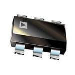
| 供应商器件封装 | SOT-23-6 |
| 关闭 | Shutdown |
| 其它名称 | ADM8828ARTZ-REEL7-ND |
| 包装 | 带卷 (TR) |
| 同步整流器 | 无 |
| 商标 | Analog Devices |
| 安装类型 | 表面贴装 |
| 宽度 | 1.6 mm |
| 封装 | Reel |
| 封装/外壳 | SOT-23-6 |
| 封装/箱体 | SOT-23-6 |
| 工作温度 | -40°C ~ 85°C |
| 工厂包装数量 | 3000 |
| 开关频率 | 120 kHz |
| 拓扑结构 | Inverting |
| 最大工作温度 | + 85 C |
| 最大输入电压 | 5.5 V |
| 最小工作温度 | - 40 C |
| 标准包装 | 3,000 |
| 电压-输入 | 1.5 V ~ 5.5 V |
| 电压-输出 | -1.5 V ~ -5.5 V |
| 电流-输出 | 25mA |
| 电源电流 | 1 mA |
| 类型 | Charge Pumps |
| 系列 | ADM8828 |
| 视频文件 | http://www.digikey.cn/classic/video.aspx?PlayerID=1364138032001&width=640&height=505&videoID=2245193149001 |
| 输入电压 | 1.5 V to 5.5 V |
| 输出数 | 1 |
| 输出电压 | - 1.5 V to - 5.5 V |
| 输出电流 | 25 mA |
| 输出类型 | 可调式 |
| 频率-开关 | 120kHz |


- 商务部:美国ITC正式对集成电路等产品启动337调查
- 曝三星4nm工艺存在良率问题 高通将骁龙8 Gen1或转产台积电
- 太阳诱电将投资9.5亿元在常州建新厂生产MLCC 预计2023年完工
- 英特尔发布欧洲新工厂建设计划 深化IDM 2.0 战略
- 台积电先进制程称霸业界 有大客户加持明年业绩稳了
- 达到5530亿美元!SIA预计今年全球半导体销售额将创下新高
- 英特尔拟将自动驾驶子公司Mobileye上市 估值或超500亿美元
- 三星加码芯片和SET,合并消费电子和移动部门,撤换高东真等 CEO
- 三星电子宣布重大人事变动 还合并消费电子和移动部门
- 海关总署:前11个月进口集成电路产品价值2.52万亿元 增长14.8%


PDF Datasheet 数据手册内容提取
a Switched-Capacitor Voltage Inverter with Shutdown ADM8828/ADM8829 FEATURES FUNCTIONAL BLOCK DIAGRAMS Inverts Input Supply Voltage 99% Voltage Conversion Efficiency 25 mA Output Current OUT 1 6 CAP+ ADM8828 Shutdown Function IN 2 TOP VIEW 5 SHDN Requires Only Two Capacitors CAP– 3 (Not to Scale) 4 GND 1 mF Capacitors 18 V Output Resistance +1.5 V to +5.5 V Input Range OUT 1 6 CAP+ ADM8829 600 mA Quiescent Current IN 2 5 NC TOP VIEW 20 nA Shutdown Current (ADM8828) CAP– 3 (Not to Scale) 4 GND APPLICATIONS NC = NO CONNECT Handheld Instruments LCD Panels Cellular Phones PDAs Remote Data Acquisition Op Amp Power Supplies GENERAL DESCRIPTION +1.5V TO +5.5V The ADM8828/ADM8829 is a charge-pump voltage inverter INPUT which may be used to generate a negative supply from a positive CAP+ input. Input voltages ranging from +1.5 V to +5.5 V can be IN inverted into a negative –1.5 V to –5.5 V output supply. This C1+ ADM8828/ 1mF ADM8829 inverting scheme is ideal for generating a negative rail in single SHUTDOWN SHDN power-supply systems. Only two small external capacitors are CAP– CONTROL needed for the charge pump. Output currents up to 25 mA with INVERTED greater than 99% efficiency are achievable. GND OUT NEGATIVE C2 OUTPUT The ADM8828 also features a low power shutdown (SHDN) +1mF pin. This can be used to disable the device and reduce the quies- cent current to 20nA. Figure 1.Typical Circuit Configuration The ADM8828/ADM8829 is available in a 6-lead SOT-23 package. REV.A Information furnished by Analog Devices is believed to be accurate and reliable. However, no responsibility is assumed by Analog Devices for its use, nor for any infringements of patents or other rights of third parties One Technology Way, P.O. Box 9106, Norwood, MA 02062-9106, U.S.A. which may result from its use. No license is granted by implication or Tel: 781/329-4700 World Wide Web Site: http://www.analog.com otherwise under any patent or patent rights of Analog Devices. Fax: 781/326-8703 © Analog Devices, Inc., 1999
ADM8828/ADM8829–SPECIFICATIONS (V = +5 V, C1, C2 = 1 mF,1 T = T to T unless other- IN A MIN MAX wise noted) Parameter Min Typ Max Units Test Conditions/Comments Input Voltage, IN 1.5 5.5 V R = 10 kW L Supply Current 600 1000 m A Unloaded Output Current 25 mA Output Resistance 18 28 W I = 5 mA L Output Ripple 25 mV p-p I = 5 mA L 130 mV p-p I = 25 mA L Charge-Pump Frequency 50 120 190 kHz 65 kHz V = +2.25 V IN Power Efficiency 90 % R = 200 W L 87 % R = 1 kW L Voltage Conversion Efficiency 99.5 99.96 % No Load 98 % R = 1 kW L 91 % R = 200 W L Shutdown Supply Current, I 0.02 2 m A SHDN = IN SHDN Shutdown Input Voltage, V 2.0 V SHDN High = Disabled SHDN 0.8 V SHDN Low = Enabled Shutdown Exit Time 175 m s I = 5 mA L NOTES 1C1 and C2 are low ESR (<0.2 W ) electrolytic capacitors. High ESR will degrade performance. Specifications subject to change without notice. ABSOLUTE MAXIMUM RATINGS* PIN FUNCTION DESCRIPTIONS (T = +25(cid:176) C unless otherwise noted) A Mnemonic Function InputVoltage (IN to GND) . . . . . . . . . . . . . . . –0.3 V to +6 V OUT to GND . . . . . . . . . . . . . . . . . . . . . . . . –6.0 V to +0.3 V CAP+ Positive Charge-Pump Capacitor Terminal. OUT, IN Output Current (Continuous) . . . . . . . . . . . . 50 mA GND Power Supply Ground. Output Short Circuit Duration to GND . . . . . . . . . . . 10 secs CAP– Negative Charge-Pump Capacitor Terminal. Power Dissipation, RT-6 . . . . . . . . . . . . . . . . . . . . . . 570 mW OUT Output, Negative Voltage. (Derate 8.3 mW/(cid:176) C above +70(cid:176) C) SHDN Shutdown Control Input. This input, when q , Thermal Impedance . . . . . . . . . . . . . . . . . . . . 120(cid:176) C/W JA high, is used to disable the charge pump Operating Temperature Range thereby reducing the power consumption. Industrial (A Version) . . . . . . . . . . . . . . . . –40(cid:176) C to +85(cid:176) C Storage Temperature Range . . . . . . . . . . . –65(cid:176) C to +150(cid:176) C IN Positive Power Supply Input. Lead Temperature Range (Soldering10sec) . . . . . . . . +300(cid:176) C Vapor Phase (70 sec) . . . . . . . . . . . . . . . . . . . . . . . . +215(cid:176) C Infrared (15 sec) . . . . . . . . . . . . . . . . . . . . . . . . . . . . +220(cid:176) C PIN CONFIGURATIONS ESD Rating . . . . . . . . . . . . . . . . . . . . . . . . . . . . . . . . >3500 V *This is a stress rating only and functional operation of the device at these or any other conditions above those indicated in the operation section of this specification OUT 1 6 CAP+ is not implied. Exposure to absolute maximum rating conditions for extended IN 2 ADM8828 5 SHDN periods may affect device reliability. TOP VIEW CAP– 3 (Not to Scale) 4 GND ORDERING GUIDE Temperature Branding Package OUT 1 6 CAP+ Model Range Information Option* ADM8829 IN 2 5 NC TOP VIEW ADM8828ART –40(cid:176) C to +85(cid:176) C MM0 RT-6 CAP– 3 (Not to Scale) 4 GND ADM8829ART –40(cid:176) C to +85(cid:176) C MN0 RT-6 NC = NO CONNECT *RT-6 = 6-lead SOT-23. –2– REV. A
Typical Performance Characteristics–ADM8828/ADM8829 0.8 60 IL = 5mA 0.7 p V p- 50 OUTPUT VOLTAGE RIPPLE mA0.6 – m @ VIN = 4.75V NT – 0.5 PPLE 40 RRE0.4 E RI 30 OUTPUT VOLTAGE RIPPLE CU AG @ VIN = 1.9V UPPLY 0.3 T VOLT 20 S0.2 PU 0.1 OUT 10 O@U VTIPN U=T 3 V.1O5LVTAGE RIPPLE 0 0 1 1.5 2 2.5 3 3.5 4 4.5 5 5.5 0.47 1 2.2 3.3 SUPPLY VOLTAGE – V CAPACITANCE – mF Figure 2.Power Supply Current vs. Voltage Figure 5.Output Voltage Ripple vs. Capacitance 35 350 30 p 300 p- OUTPUT VOLTAGE RIPPLE V mV @ VIN = 4.75V, VOUT = –4.0V NCE – 25 PLE – 250 ESISTA 20 GE RIP 200 O@U VTIPN U=T 3 V.1O5LVT, AVOGUET R=I P–P2.L5EV UT R 15 OLTA 150 OUTP 10 UT V 100 P T U 5 O 50 OUTPUT VOLTAGE RIPPLE @ VIN = 1.9V, VOUT = –1.5V 0 0 1.5 2 2.5 3 3.5 4 4.5 5 5.5 0.47 1 2.2 3.3 SUPPLY VOLTAGE – V CAPACITANCE – mF Figure 3.Output Source Resistance vs. Supply Voltage Figure 6.Output Voltage Ripple vs. Capacitance 20 0 18 OUTPUT CURRENT @ VIN = 4.75V –0.5 OUTPUT VOLTAGE @ VIN = 2.0V 16 –1 A OUTPUT CURRENT – m 11186204 OOUUTTPPUUTT CCUURRRREENNTT @@ VVIINN == 31..195VV OUTPUT VOLTAGE – V –––231––...55532 OUTPUT VOLTAGE @ VIN = 3.3V 4 –4 OUTPUT VOLTAGE @ VIN = 5.0V 2 –4.5 0 –5 0.47 1 2.2 3.3 0 5 10 15 20 25 30 35 40 45 CAPACITANCE – mF OUTPUT CURRENT – mA Figure 4.Output Current vs. Capacitance Figure 7.Output Voltage vs. Output Current REV. A –3–
ADM8828/ADM8829 100 200 PEFF @ VIN = 5.0V 90 180 80 160 PUMP FREQUENCY 70 kHz140 @ VIN = 3.3V – % 60 PEFF @ VIN = 2.0VPEFF @ VIN = 3.3V ENCY – 120 P@U VMINP =F R5.E0QVUENCY F50 U100 F Q PE40 P FRE 80 P@U VMINP =F R1.E5QVUENCY 30 UM 60 P 20 40 10 20 0 0 0 5 10 15 20 25 30 35 40 45 50 –50 –30 –10 10 25 40 60 80 90 110 125 IOUT – mA TEMPERATURE – 8C Figure 8.Power Efficiency vs. Output Current Figure 10.Charge Pump Frequency vs. Temperature 50 45 RESISTANCE (V) @ VIN = 1.5V 40 V E – 35 C STAN 30 RESISTANCE (V) @ VIN = 3.3V SI 25 E R T 20 U UTP 15 RESISTANCE (V) @ VIN = 5.0V O 10 5 0 –50 –30 –10 10 25 40 60 80 90 110 125 TEMPERATURE – 8C Figure 9.Output Resistance vs. Temperature –4– REV. A
ADM8828/ADM8829 GENERAL INFORMATION Capacitor Selection The ADM8828/ADM8829 is a switched capacitor voltage con- The flying capacitor C1 can be increased to reduce the output verter that can be used to invert the input supply voltage. resistance. The voltage conversion task is achieved using a switched capaci- The output capacitor size C2 affects the output ripple. Increas- tor technique using two external charge storage capacitors. An ing the capacitor size reduces the peak-peak ripple. The ESR on-chip oscillator and switching network transfers charge between affects both the output impedance and the output ripple. the charge storage capacitors. The basic principle behind the Reducing the ESR reduces the output impedance and ripple. voltage conversion scheme is illustrated below. For convenience it is recommended that both C1 and C2 be the same value. S1 CAP+ S3 V+ The ac impedance of the ADM8828/ADM8829 may be reduced + S2 C1 S4 by using a bypass capacitor on the input supply. This capacitor OUT = –V+ CAP– + should be connected between the input supply and GND. It will C2 provide instantaneous current surges as required. Suitable capaci- F1 OSCI4LL 2ATOR F2 tors of 1 m F or greater may be used. Figure 11.Voltage Inversion Principle +1.5V TO +5.5V An oscillator generating antiphase signals f 1 and f 2 controls INPUT switches S1, S2 and S3, S4. During f 1, switches S1 and S2 are closed while S3 and S4 are open, thereby charging C1 up to the CAP+ IN voltage at V+. During f 2, S1 and S2 open and S3 and S4 close. C1+ ADM8828/ 1mF ADM8829 The positive terminal of C1 is connected to GND via S3 during SHDN SHUTDOWN this phase and the negative terminal of C1 connects to V CAP– CONTROL OUT via S4. The net result is voltage inversion at V wrt GND. OUT INVERTED Charge on C1 is transferred to C2 during f 2. Capacitor C2 GND OUT NEGATIVE maintains this voltage during f 1. The charge transfer efficiency +C1m2F OUTPUT depends on the on-resistance of the switches, the frequency at which they are being switched and also on the equivalent series Figure 12.Typical Circuit Configuration resistance (ESR) of the external capacitors. For maximum effi- ciency, capacitors with low ESR are, therefore, recommended. Shutdown Input The ADM8828 contains a shutdown input that can be used to disable the device and hence reduce the power consumption. A logic high level on the SHDN input shuts the device down reducing the quiescent current to 0.02 m A. During shutdown the output voltage discharges to 0 V. Therefore, ground ref- erenced loads are not powered during this state. When exiting shutdown, it takes several cycles (approximately 175 m s) for the charge pump to reach its final value. If the shutdown function is not being used, SHDN should be hardwired to GND. REV. A –5–
ADM8828/ADM8829 OUTLINE DIMENSIONS Dimensions shown in inches and (mm). 6-Lead SOT-23 (RT-6) 0.122 (3.10) 0.106 (2.70) 9 9 0/ 1 – 0 0.071 (1.80) 6 5 4 0.118 (3.00) 2a– 0.059 (1.50) 0.098 (2.50) 35 1 2 3 3 C PIN 1 0.037 (0.95) BSC 0.075 (1.90) BSC 0.051 (1.30) 0.057 (1.45) 0.035 (0.90) 0.035 (0.90) 108 0.006 (0.15) 0.020 (0.50) SEATING 0.009 (0.23) 08 0.022 (0.55) 0.000 (0.00) 0.010 (0.25) PLANE 0.003 (0.08) 0.014 (0.35) A. S. U. N I D E T N RI P –6– REV. A
Mouser Electronics Authorized Distributor Click to View Pricing, Inventory, Delivery & Lifecycle Information: A nalog Devices Inc.: ADM8828ART-REEL ADM8828ARTZ-REEL7 ADM8829ARTZ-REEL ADM8829ARTZ-REEL7