ICGOO在线商城 > 集成电路(IC) > PMIC - 稳压器 - DC DC 开关稳压器 > TPS62132RGTR
 Datasheet下载
- 型号: TPS62132RGTR
- 制造商: Texas Instruments
- 库位|库存: xxxx|xxxx
- 要求:
| 数量阶梯 | 香港交货 | 国内含税 |
| +xxxx | $xxxx | ¥xxxx |
查看当月历史价格
查看今年历史价格
TPS62132RGTR产品简介:
ICGOO电子元器件商城为您提供TPS62132RGTR由Texas Instruments设计生产,在icgoo商城现货销售,并且可以通过原厂、代理商等渠道进行代购。 TPS62132RGTR价格参考。Texas InstrumentsTPS62132RGTR封装/规格:PMIC - 稳压器 - DC DC 开关稳压器, Buck Switching Regulator IC Positive Fixed 3.3V 1 Output 3A 16-VFQFN Exposed Pad。您可以下载TPS62132RGTR参考资料、Datasheet数据手册功能说明书,资料中有TPS62132RGTR 详细功能的应用电路图电压和使用方法及教程。
TPS62132RGTR是Texas Instruments(德州仪器)推出的一款高效、同步降压型DC-DC开关稳压器,广泛应用于需要高效率和小尺寸电源解决方案的场景。其主要应用场景包括便携式设备、工业电子、通信系统及消费类电子产品。

在便携式设备中,如智能手机、平板电脑和可穿戴设备,TPS62132RGTR凭借高达2.5MHz的开关频率和高达95%的转换效率,能够在有限空间内提供稳定电源,同时延长电池续航时间。其轻载高效脉冲跳跃模式显著降低待机功耗,非常适合对能效要求严苛的应用。

在工业自动化与控制系统中,该器件可用于为微控制器(MCU)、传感器、FPGA及低功耗处理器供电,其宽输入电压范围(3V至17V)和良好的负载瞬态响应能力确保系统在复杂环境下稳定运行。

此外,在网络通信设备(如路由器、交换机)和分布式电源系统中,TPS62132RGTR的小尺寸QFN封装(6引脚)便于实现高密度布局,支持多层PCB设计,有助于缩小整体电源模块体积。

总之,TPS62132RGTR适用于各类对效率、尺寸和可靠性有较高要求的中低功率DC-DC转换应用,是现代电子设备中理想的电源管理解决方案之一。
| 参数 | 数值 |
| 产品目录 | 集成电路 (IC)半导体 |
| 描述 | IC REG BUCK SYNC 3.3V 3A 16QFN稳压器—开关式稳压器 3-17V 3A SD Cnvrtr |
| 产品分类 | |
| 品牌 | Texas Instruments |
| 产品手册 | |
| 产品图片 |
|
| rohs | 符合RoHS无铅 / 符合限制有害物质指令(RoHS)规范要求 |
| 产品系列 | 电源管理 IC,稳压器—开关式稳压器,Texas Instruments TPS62132RGTRDCS-Control™ |
| 数据手册 | |
| 产品型号 | TPS62132RGTR |
| PCN设计/规格 | |
| PWM类型 | 混合物 |
| 产品种类 | 稳压器—开关式稳压器 |
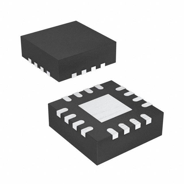
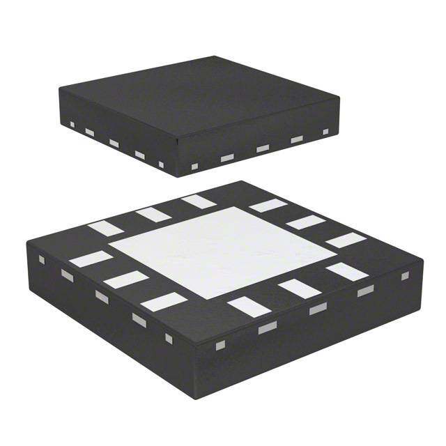
| 供应商器件封装 | 16-QFN(3x3) |
| 其它名称 | 296-29936-6 |
| 制造商产品页 | http://www.ti.com/general/docs/suppproductinfo.tsp?distId=10&orderablePartNumber=TPS62132RGTR |
| 包装 | Digi-Reel® |
| 同步整流器 | 是 |
| 商标 | Texas Instruments |
| 安装类型 | 表面贴装 |
| 安装风格 | SMD/SMT |
| 封装 | Reel |
| 封装/外壳 | 16-VFQFN 裸露焊盘 |
| 封装/箱体 | VQFN-16 |
| 工作温度 | -40°C ~ 85°C |
| 工作温度范围 | - 40 C to + 85 C |
| 工厂包装数量 | 3000 |
| 开关频率 | 2.5 MHz |
| 拓扑结构 | Buck |
| 最大工作温度 | + 85 C |
| 最大输入电压 | 17 V |
| 最小工作温度 | - 40 C |
| 最小输入电压 | 3 V |
| 标准包装 | 1 |
| 电压-输入 | 3 V ~ 17 V |
| 电压-输出 | 3.3V |
| 电流-输出 | 3A |
| 类型 | 降压(降压) |
| 系列 | TPS62132 |
| 设计资源 | http://www.digikey.com/product-highlights/cn/zh/texas-instruments-webench-design-center/3176 |
| 输入电压 | 3 V to 17 V |
| 输出数 | 1 |
| 输出电压 | 3.3 V |
| 输出电流 | 3 A |
| 输出端数量 | 1 Output |
| 输出类型 | 固定 |
| 频率-开关 | 2.5MHz |


.jpg)


PDF Datasheet 数据手册内容提取
Product Order Technical Tools & Support & Folder Now Documents Software Community TPS62130,TPS62130A,TPS62131,TPS62132,TPS62133 SLVSAG7E–NOVEMBER2011–REVISEDAUGUST2016 TPS6213x 3-V to17-V, 3-A Step-Down Converter In 3x3 QFN Package 1 Features 3 Description • DCS-Control™Topology The TPS6213X family is an easy to use synchronous 1 step down DC-DC converter optimized for • InputVoltageRange:3to17V applications with high power density. A high switching • Upto3AOutputCurrent frequency of typically 2.5MHz allows the use of small • AdjustableOutputVoltagefrom0.9to6V inductorsandprovidesfasttransientresponseaswell as high output voltage accuracy by use of the DCS- • Pin-SelectableOutputVoltage(nominal,+5%) Control™topology. • ProgrammableSoftStartandTracking With their wide operating input voltage range of 3V to • SeamlessPowerSaveModeTransition 17V, the devices are ideally suited for systems • QuiescentCurrentof17µA(typ.) powered from either a Li-Ion or other batteries as well • SelectableOperatingFrequency as from 12V intermediate power rails. It supports up to 3A continuous output current at output voltages • PowerGoodOutput between 0.9V and 6V (with 100% duty cycle mode). • 100%DutyCycleMode The output voltage startup ramp is controlled by the • ShortCircuitProtection soft-start pin, which allows operation as either a • OverTemperatureProtection standalonepowersupplyorintrackingconfigurations. Power sequencing is also possible by configuring the • PintoPinCompatiblewithTPS62140and Enableandopen-drainPowerGoodpins. TPS62150 In Power Save Mode, the devices draw quiescent • Availableina3× 3mm,QFN-16Package current of about 17μA from V . Power Save Mode, IN entered automatically and seamlessly if load is small, 2 Applications maintains high efficiency over the entire load range. • Standard12-VRailSupplies In Shutdown Mode, the device is turned off and shutdowncurrentconsumptionislessthan2μA. • POLSupplyfromSingleorMultipleLi-IonBattery • Solid-StateDiskDrives The device, available in adjustable and fixed output voltage versions, is packaged in a 16-pin VQFN • EmbeddedSystems packagemeasuring3×3mm(RGT). • LDOreplacement • MobilePCs,Tablet,Modems,Cameras DeviceInformation(1) • Server,Microserver PARTNUMBER PACKAGE BODYSIZE(NOM) • DataTerminal,PointofSales(ePOS) TPS6213x VQFN(16) 3.00mm×3.00mm (1) For all available packages, see the orderable addendum at theendofthedatasheet. TypicalApplicationSchematic EfficiencyvsOutputCurrent (3..17)V 1/2.2µH 1.8V/3A 100 PVIN SW AVIN VOS 100kΩ 90 10μF 0.1μF EN PG 22μF SS/TR TPS62131 FB %) 80 VIN=5V VIN=12V VIN=17V 3.3nF DEF AGND ncy ( 70 FSW PGND cie Effi 60 Copyright © 2016,Texas Instruments Incorporated 50 VOUT=3.3V fsw=1.25MHz 40 0.0 0.5 1.0 1.5 2.0 2.5 3.0 Output Current (A) G001 1 An IMPORTANT NOTICE at the end of this data sheet addresses availability, warranty, changes, use in safety-critical applications, intellectualpropertymattersandotherimportantdisclaimers.PRODUCTIONDATA.
TPS62130,TPS62130A,TPS62131,TPS62132,TPS62133 SLVSAG7E–NOVEMBER2011–REVISEDAUGUST2016 www.ti.com Table of Contents 1 Features.................................................................. 1 9.1 ApplicationInformation............................................13 2 Applications........................................................... 1 9.2 TypicalApplication .................................................13 3 Description............................................................. 1 9.3 SystemExamples...................................................25 4 RevisionHistory..................................................... 2 10 PowerSupplyRecommendations..................... 29 5 DeviceComparisonTable..................................... 4 11 Layout................................................................... 30 11.1 LayoutGuidelines.................................................30 6 PinConfigurationandFunctions......................... 4 11.2 LayoutExample....................................................30 7 Specifications......................................................... 5 11.3 ThermalInformation..............................................31 7.1 AbsoluteMaximumRatings......................................5 12 DeviceandDocumentationSupport................. 32 7.2 ESDRatings ............................................................5 12.1 DeviceSupport ....................................................32 7.3 RecommendedOperatingConditions.......................5 12.2 DocumentationSupport .......................................32 7.4 ThermalInformation..................................................5 12.3 ReceivingNotificationofDocumentationUpdates32 7.5 ElectricalCharacteristics...........................................6 12.4 RelatedLinks........................................................32 7.6 TypicalCharacteristics..............................................7 12.5 CommunityResources..........................................33 8 DetailedDescription.............................................. 8 12.6 Trademarks...........................................................33 8.1 Overview...................................................................8 12.7 ElectrostaticDischargeCaution............................33 8.2 FunctionalBlockDiagram.........................................8 12.8 Glossary................................................................33 8.3 FeatureDescription...................................................9 13 Mechanical,Packaging,andOrderable 8.4 DeviceFunctionalModes........................................11 Information........................................................... 33 9 ApplicationandImplementation........................ 13 4 Revision History NOTE:Pagenumbersforpreviousrevisionsmaydifferfrompagenumbersinthecurrentversion. ChangesfromRevisionD(June2016)toRevisionE Page • ChangedtheT MAXvalueFrom:125°CTo:150°CintheAbsoluteMaximumRatings ..................................................... 5 J • Changed(T =–40°Cto85°C)To:(T =–40°Cto125°C)intheElectricalCharacteristicsconditions................................ 6 J J • AddedatestconditionforI atT =-40°Cto+85°CintheElectricalCharacteristics........................................................... 6 Q A • AddedTable1andTable2 ................................................................................................................................................. 10 ChangesfromRevisionC(January2015)toRevisionD Page • Added"PintoPinCompatiblewithTPS62140andTPS62150"toFeatureslist .................................................................. 1 • Added"Server,Microserver";and,"DataTerminal,PointofSales(ePOS)"toApplicationslist........................................... 1 • ChangedtheDeviceComparisonTableformat..................................................................................................................... 4 • ChangedThermalInformationtable ...................................................................................................................................... 5 • AddedSwitchingFrequencygraphsfor1.0-V,1.8-V,and5.0-Vapplications..................................................................... 20 • CorrectedSystemExamplesschematics............................................................................................................................. 25 • ChangedLayoutExamplepictorial....................................................................................................................................... 30 • AddedCommunityResourcessection ................................................................................................................................ 33 ChangesfromRevisionB(June2013)toRevisionC Page • AddedDeviceInformationandESDRatingtables,FeatureDescriptionsection,DeviceFunctionalModes, Programmingsection,ApplicationandImplementationsection,PowerSupplyRecommendationssection,Layout section,DeviceandDocumentationSupportsection,andMechanical,Packaging,andOrderableInformation section ................................................................................................................................................................................... 1 • Added"(PWMmodeoperation)"textstringtoV specTestConditionsforclarification.................................................. 6 UVLO • ChangedsecondparagraphofSS/TRdescriptionforclarification. .................................................................................... 10 2 SubmitDocumentationFeedback Copyright©2011–2016,TexasInstrumentsIncorporated
TPS62130,TPS62130A,TPS62131,TPS62132,TPS62133 www.ti.com SLVSAG7E–NOVEMBER2011–REVISEDAUGUST2016 ChangesfromRevisionA(September2012)toRevisionB Page • AddeddeviceTPS62130AtodatasheetHeader................................................................................................................... 1 • AddeddeviceTPS62130AtoDeviceComparisontable........................................................................................................ 4 • AddedtexttoPowerGoodsectionregardingTPS63130A.................................................................................................. 10 • AddedpinoptiontoFootnotestatementforPin-SelectableOutputVoltage(DEF)section................................................. 10 • AddedtexttoFrequencySelection(FSW)sectionregardingpincontrol............................................................................. 11 • AddedtexttoTrackingFunctionsectionforclarification...................................................................................................... 17 • AddedapplicationexampleregardingTPS62130Adevice.................................................................................................. 25 Copyright©2011–2016,TexasInstrumentsIncorporated SubmitDocumentationFeedback 3
TPS62130,TPS62130A,TPS62131,TPS62132,TPS62133 SLVSAG7E–NOVEMBER2011–REVISEDAUGUST2016 www.ti.com 5 Device Comparison Table PARTNUMBER OUTPUTVOLTAGE PowerGoodLogicLevel(EN=Low) TPS62130 adjustable HighImpedance TPS62130A adjustable Low TPS62131 1.8V HighImpedance TPS62132 3.3V HighImpedance TPS62133 5.0V HighImpedance 6 Pin Configuration and Functions 16-PinVQFNWithExposedThermalPad(RGT) TopView D D N N S G G O N P P V E 16 15 14 13 SW 1 12 PVIN SW 2 11 PVIN Exposed Thermal Pad SW 3 10 AVIN PG 4 9 SS/TR 5 6 7 8 B D W F F GN FS DE A PinFunctions PIN(1) I/O DESCRIPTION NO. NAME 1,2,3 SW O Switchnode,whichisconnectedtotheinternalMOSFETswitches.ConnectinductorbetweenSWand outputcapacitor. 4 PG O Outputpowergood(High=V ready,Low=V belownominalregulation);opendrain(requires OUT OUT pull-upresistor) 5 FB I Voltagefeedbackofadjustableversion.Connectresistivevoltagedividertothispin.Itisrecommended toconnectFBtoAGNDonfixedoutputvoltageversionsforimprovedthermalperformance. 6 AGND AnalogGround.MustbeconnecteddirectlytotheExposedThermalPadandcommongroundplane. 7 FSW I SwitchingFrequencySelect(Low≈2.5MHz,High≈1.25MHz(2)fortypicaloperation)(3) 8 DEF I OutputVoltageScaling(Low=nominal,High=nominal+5%)(3) Soft-Start/TrackingPin.Anexternalcapacitorconnectedtothispinsetstheinternalvoltagereference 9 SS/TR I risetime.Itcanbeusedfortrackingandsequencing. 10 AVIN I Supplyvoltageforcontrolcircuitry.ConnecttosamesourceasPVIN. 11,12 PVIN I Supplyvoltageforpowerstage.ConnecttosamesourceasAVIN. 13 EN I Enableinput(High=enabled,Low=disabled)(3) 14 VOS I Outputvoltagesensepinandconnectionforthecontrolloopcircuitry. 15,16 PGND PowerGround.MustbeconnecteddirectlytotheExposedThermalPadandcommongroundplane. Exposed MustbeconnectedtoAGND(pin6),PGND(pin15,16)andcommongroundplane.SeetheLayout ThermalPad Example.Mustbesolderedtoachieveappropriatepowerdissipationandmechanicalreliability. (1) Formoreinformationaboutconnectingpins,seeDetailedDescriptionandApplicationandImplementationsections. (2) ConnectFSWtoV orPGinthiscase. OUT (3) Aninternalpull-downresistorkeepslogiclevellow,ifpinisfloating. 4 SubmitDocumentationFeedback Copyright©2011–2016,TexasInstrumentsIncorporated
TPS62130,TPS62130A,TPS62131,TPS62132,TPS62133 www.ti.com SLVSAG7E–NOVEMBER2011–REVISEDAUGUST2016 7 Specifications 7.1 Absolute Maximum Ratings(1) overoperatingjunctiontemperaturerange(unlessotherwisenoted) MIN MAX UNIT AVIN,PVIN –0.3 20 V EN,SS/TR –0.3 V +0.3 Pinvoltagerange(2) IN SW –0.3 V +0.3 V IN DEF,FSW,FB,PG,VOS –0.3 7 V PowerGoodsinkcurrent PG 10 mA Operatingjunctiontemperature,T –40 150 °C J Storagetemperature,T –65 150 °C stg (1) Stressesbeyondthoselistedunderabsolutemaximumratingsmaycausepermanentdamagetothedevice.Thesearestressratings only,andfunctionaloperationofthedeviceattheseoranyotherconditionsbeyondthoseindicatedunderrecommendedoperating conditionsisnotimplied.Exposuretoabsolute-maximum-ratedconditionsforextendedperiodsmayaffectdevicereliability. (2) Allvoltagesarewithrespecttonetworkgroundterminal. 7.2 ESD Ratings VALUE UNIT Human-bodymodel(HBM),perANSI/ESDA/JEDECJS-001(2) ±2000 V(ESD) Electrostaticdischarge(1) Charged-devicemodel(CDM),perJEDECspecificationJESD22- V C101(3) ±500 (1) ESDtestingisperformedaccordingtotherespectiveJESD22JEDECstandard. (2) JEDECdocumentJEP155statesthat500-VHBMallowssafemanufacturingwithastandardESDcontrolprocess. (3) JEDECdocumentJEP157statesthat250-VCDMallowssafemanufacturingwithastandardESDcontrolprocess. 7.3 Recommended Operating Conditions overoperatingjunctiontemperaturerange(unlessotherwisenoted) MIN MAX UNIT SupplyVoltage,V (atAVINandPVIN) 3 17 V IN Operatingjunctiontemperature,T –40 125 °C J 7.4 Thermal Information TPS6213X THERMALMETRIC(1) UNITS RGT16PINS R Junction-to-ambientthermalresistance 45 θJA R Junction-to-case(top)thermalresistance 53.6 θJCtop R Junction-to-boardthermalresistance 17.4 θJB °C/W ψ Junction-to-topcharacterizationparameter 1.1 JT ψ Junction-to-boardcharacterizationparameter 17.4 JB R Junction-to-case(bottom)thermalresistance 4.5 θJCbot (1) Formoreinformationabouttraditionalandnewthermalmetrics,seetheSemiconductorandICPackageThermalMetricsapplication report. Copyright©2011–2016,TexasInstrumentsIncorporated SubmitDocumentationFeedback 5
TPS62130,TPS62130A,TPS62131,TPS62132,TPS62133 SLVSAG7E–NOVEMBER2011–REVISEDAUGUST2016 www.ti.com 7.5 Electrical Characteristics overoperatingjunctiontemperature(T =–40°Cto125°C),typicalvaluesatV =12VandT =25°C(unlessotherwisenoted) J IN A PARAMETER TESTCONDITIONS MIN TYP MAX UNIT SUPPLY V Inputvoltagerange(1) 3 17 V IN EN=High,I =0mA, 17 30 I Operatingquiescentcurrent OUT µA Q devicenotswitching T =-40°Cto+85°C 17 25 A I 1.5 25 SD Shutdowncurrent(2) EN=Low µA T =-40°Cto+85°C 1.5 4 A V FallingInputVoltage(PWMmodeoperation) 2.6 2.7 2.8 V UVLO Undervoltagelockoutthreshold Hysteresis 200 mV T Thermalshutdowntemperature 160 SD °C Thermalshutdownhysteresis 20 CONTROL(EN,DEF,FSW,SS/TR,PG) Highlevelinputthresholdvoltage(EN, V 0.9 0.65 V H DEF,FSW) V Lowlevelinputthresholdvoltage(EN, 0.45 L 0.3 V DEF,FSW) I Inputleakagecurrent(EN,DEF,FSW) EN=V orGND;DEF,FSW=V orGND 0.01 1 µA LKG IN OUT Rising(%V ) 92% 95% 98% OUT V Powergoodthresholdvoltage TH_PG Falling(%V ) 87% 90% 94% OUT V Powergoodoutputlow I =–2mA 0.07 0.3 V OL_PG PG I Inputleakagecurrent(PG) V =1.8V 1 400 nA LKG_PG PG I SS/TRpinsourcecurrent 2.3 2.5 2.7 µA SS/TR POWERSWITCH V ≥6V 90 170 IN High-sideMOSFETON-resistance mΩ V =3V 120 IN R DS(ON) V ≥6V 40 70 IN Low-sideMOSFETON-resistance mΩ V =3V 50 IN High-sideMOSFETforwardcurrent V =12V,T =25°C ILIMF limit(3) IN A 3.6 4.2 4.9 A OUTPUT I Inputleakagecurrent(FB) TPS62130,V =0.8V 1 100 nA LKG_FB FB Outputvoltagerange(TPS62130) V ≥V 0.9 6.0 V IN OUT DEF(Outputvoltageprogramming) DEF=0(GND) V OUT DEF=1(V ) V +5% OUT OUT PWMmodeoperation,V ≥V +1V 785.6 800 814.4 IN OUT PWMmodeoperation,V ≥V +1V, Initialoutputvoltageaccuracy(4) IN OUT 788.0 800 812.8 mV VOUT TA=–10°Cto85°C PowerSaveModeoperation,C =22µF 781.6 800 822.4 OUT TrackingFeedbackVoltage(TPS62130) V =350mV 212.6 225 237.4 mV SS/TR Loadregulation(5) V =12V,V =3.3V,PWMmodeoperation 0.05 %/A IN OUT Lineregulation(5) 3V≤VIN≤17V,VOUT=3.3V,IOUT=1A,PWM 0.02 %/V modeoperation (1) ThedeviceisstillfunctionaldowntoUnderVoltageLockout(seeparameterV ). UVLO (2) CurrentintoAVIN+PVINpin. (3) Thisisthestaticcurrentlimit.Itcanbetemporarilyhigherinapplicationsduetointernalpropagationdelay(seeCurrentLimitAndShort CircuitProtectionsection). (4) ThisistheaccuracyprovidedattheFBpinfortheadjustableV version(lineandloadregulationeffectsarenotincluded).Forthe OUT fixedoutputvoltageversionsthe(internal)resistivedividerisincluded. (5) Lineandloadregulationdependonexternalcomponentselectionandlayout(seeFigure22andFigure23). 6 SubmitDocumentationFeedback Copyright©2011–2016,TexasInstrumentsIncorporated
TPS62130,TPS62130A,TPS62131,TPS62132,TPS62133 www.ti.com SLVSAG7E–NOVEMBER2011–REVISEDAUGUST2016 7.6 Typical Characteristics Figure1.QuiescentCurrent Figure2.ShutdownCurrent 200.0 100.0 180.0 ) 160.0 125°C ) 80.0 WSide (m 112400..00 85°C WSide (m 60.0 85°C 125°C h− 100.0 25°C w− DSon Hig 6800..00 −10°C DSon Lo 40.0 −251°0C°C R 40.0 −40°C R 20.0 −40°C 20.0 0.0 0.0 0.0 3.0 6.0 9.0 12.0 15.0 18.0 20.0 0.0 3.0 6.0 9.0 12.0 15.0 18.0 20.0 Input Voltage (V) Input Voltage (V) G001 G001 Figure3.High-SideSwitchResistance Figure4.Low-SideSwitchResistance Copyright©2011–2016,TexasInstrumentsIncorporated SubmitDocumentationFeedback 7
TPS62130,TPS62130A,TPS62131,TPS62132,TPS62133 SLVSAG7E–NOVEMBER2011–REVISEDAUGUST2016 www.ti.com 8 Detailed Description 8.1 Overview The TPS6213X synchronous switched mode power converters are based on DCS-Control™ (Direct Control with Seamless Transition into Power Save Mode), an advanced regulation topology, that combines the advantages of hysteretic, voltage mode and current mode control including an AC loop directly associated to the output voltage. This control loop takes information about output voltage changes and feeds it directly to a fast comparator stage. It sets the switching frequency, which is constant for steady state operating conditions, and provides immediate response to dynamic load changes. To get accurate DC load regulation, a voltage feedback loop is used. The internally compensated regulation network achieves fast and stable operation with small external components andlowESRcapacitors. The DCS-ControlTM topology supports PWM (Pulse Width Modulation) mode for medium and heavy load conditions and a Power Save Mode at light loads. During PWM, it operates at its nominal switching frequency in continuous conduction mode. This frequency is typically about 2.5MHz or 1.25MHz with a controlled frequency variationdependingontheinputvoltage.Iftheloadcurrentdecreases,theconverterentersPowerSaveModeto sustain high efficiency down to very light loads. In Power Save Mode the switching frequency decreases linearly with the load current. Since DCS-ControlTM supports both operation modes within one single building block, the transitionfromPWMtoPowerSaveModeisseamlesswithouteffectsontheoutputvoltage. Fixed output voltage versions provide smallest solution size and lowest current consumption, requiring only 4 externalcomponents.Aninternalcurrentlimitsupportsnominaloutputcurrentsofupto3A. The TPS6213X family offers both excellent DC voltage and superior load transient regulation, combined with verylowoutputvoltageripple,minimizinginterferencewithRFcircuits. 8.2 Functional Block Diagram PG AVIN PVIN PVIN Soft Thermal UVLO PGcontrol start Shtdwn HSlim comp EN* SW SS/TR power gate controllogic control drive SW DEF* SW FSW* comp LSlim VOS directcontrol & ramp compensation _ FB comparator timertON error + amplifier DCS-ControlTM *Thispinisconnectedtoapulldownresistorinternally AGND PGNDPGND (seeFeatureDescriptionsection). *Thispinisconnectedtoapulldownresistorinternally(seeFeatureDescriptionsection). Figure5. TPS62130andTPS62130A(AdjustableOutputVoltage) 8 SubmitDocumentationFeedback Copyright©2011–2016,TexasInstrumentsIncorporated
TPS62130,TPS62130A,TPS62131,TPS62132,TPS62133 www.ti.com SLVSAG7E–NOVEMBER2011–REVISEDAUGUST2016 Functional Block Diagram (continued) PG AVIN PVIN PVIN Soft Thermal UVLO PGcontrol start Shtdwn HSlim comp EN* SW SS/TR power gate controllogic control drive SW DEF* SW FSW* comp LSlim VOS directcontrol & ramp compensation _ FB* comparator timertON error + amplifier DCS-ControlTM *Thispinisconnectedtoapulldownresistorinternally AGND PGNDPGND (seeFeatureDescriptionsection). *Thispinisconnectedtoapulldownresistorinternally(seeFeatureDescriptionsection). Figure6. TPS62131/2/3(FixedOutputVoltage) space 8.3 Feature Description 8.3.1 Enable/Shutdown(EN) When Enable (EN) is set High, the device starts operation. Shutdown is forced if EN is pulled Low with a shutdown current of typically 1.5µA. During shutdown, the internal power MOSFETs as well as the entire control circuitry are turned off. The internal resistive divider pulls down the output voltage smoothly. The EN signal must be set externally to High or Low. An internal pull-down resistor of about 400kΩ is connected and keeps EN logic low,ifLowissetinitiallyandthenthepingetsfloating.ItisdisconnectedifthepinissetHigh. Connecting the EN pin to an appropriate output signal of another power rail provides sequencing of multiple powerrails. 8.3.2 SoftStart/Tracking(SS/TR) The internal soft start circuitry controls the output voltage slope during startup. This avoids excessive inrush current and ensures a controlled output voltage rise time. It also prevents unwanted voltage drops from high- impedance power sources or batteries. When EN is set to start device operation, the device starts switching after a delay of about 50µs and V rises with a slope controlled by an external capacitor connected to the SS/TR OUT pin.SeeFigure40andFigure41fortypicalstartupoperation. Copyright©2011–2016,TexasInstrumentsIncorporated SubmitDocumentationFeedback 9
TPS62130,TPS62130A,TPS62131,TPS62132,TPS62133 SLVSAG7E–NOVEMBER2011–REVISEDAUGUST2016 www.ti.com Feature Description (continued) Using a very small capacitor (or leaving SS/TR pin un-connected) provides fastest startup behavior. There is no theoretical limit for the longest startup time. The TPS6213X can start into a pre-biased output. During monotonic pre-biased startup, both the power MOSFETs are not allowed to turn on until the device's internal ramp sets an output voltage above the pre-bias voltage. As long as the output is below about 0.5V a reduced current limit of typically 1.6A is set internally. If the device is set to shutdown (EN=GND), undervoltage lockout or thermal shutdown,aninternalresistorpullstheSS/TRpindowntoensureaproperlowlevel.Returningfromthosestates causesanewstartupsequenceassetbytheSS/TRconnection. AvoltagesuppliedtoSS/TRcanbeusedfortrackingamastervoltage.Theoutputvoltagewillfollowthisvoltage inbothdirectionsupanddown(seeApplicationandImplementation). 8.3.3 PowerGood(PG) The TPS6213X has a built in power good (PG) function to indicate whether the output voltage has reached its appropriate level or not. The PG signal can be used for startup sequencing of multiple rails. The PG pin is an open-drain output that requires a pull-up resistor (to any voltage below 7 V). It can sink 2 mA of current and maintain its specified logic low level. With TPS62130 it is high impedance when the device is turned off due to EN, UVLO or thermal shutdown. TPS62130A features PG=Low in this case and can be used to actively discharge V (see Figure 47). V must remain present for the PG pin to stay Low. See SLVA644 for OUT IN applicationdetails.Ifnotused,thePGpinshouldbeconnectedtoGNDbutmaybeleftfloating. space Table1.PowerGoodPinLogicTable(TPS62130) PGLogicStatus DeviceState HighImpedance Low V ≥V √ FB TH_PG Enable(EN=High) V ≤V √ FB TH_PG Shutdown(EN=Low) √ UVLO 0.7V<V <V √ IN UVLO ThermalShutdown T >T √ J SD PowerSupplyRemoval V <0.7V √ IN space Table2.PowerGoodPinLogicTable(TPS62130A) PGLogicStatus DeviceState HighImpedance Low V ≥V √ FB TH_PG Enable(EN=High) V ≤V √ FB TH_PG Shutdown(EN=Low) √ UVLO 0.7V<V <V √ IN UVLO ThermalShutdown T >T √ J SD PowerSupplyRemoval V <0.7V √ IN space 8.3.4 Pin-SelectableOutputVoltage(DEF) The output voltage of the TPS6213X devices can be increased by 5% above the nominal voltage by setting the DEFpintoHigh (1).WhenDEFisLow,thedeviceregulatestothenominaloutputvoltage.Increasingthenominal voltage allows adapting the power supply voltage to the variations of the application hardware. More detailed information on voltage margining using TPS6213X can be found in SLVA489. A pull down resistor of about 400 kΩ is internally connected to the pin, to ensure a proper logic level if the pin is high impedance or floating after initiallysettoLow.TheresistorisdisconnectedifthepinissetHigh. (1) Maximumallowedvoltageis7V.Therefore,itisrecommendedtoconnectittoV orPG,notV . OUT IN 10 SubmitDocumentationFeedback Copyright©2011–2016,TexasInstrumentsIncorporated
TPS62130,TPS62130A,TPS62131,TPS62132,TPS62133 www.ti.com SLVSAG7E–NOVEMBER2011–REVISEDAUGUST2016 8.3.5 FrequencySelection(FSW) To get high power density with very small solution size, a high switching frequency allows the use of small external components for the output filter. However switching losses increase with the switching frequency. If efficiency is the key parameter, more than solution size, the switching frequency can be set to half (1.25 MHz typ.) by pulling FSW to High. It is mandatory to start with FSW=Low to limit inrush current, which can be done by connecting to V or PG. Running with lower frequency a higher efficiency, but also a higher output voltage OUT ripple, is achieved. Pull FSW to Low for high frequency operation (2.5 MHz typ.). To get low ripple and full output current at the lower switching frequency, it's recommended to use an inductor of at least 2.2 µH. The switching frequency can be changed during operation, if needed. A pull down resistor of about 400kOhm is internally connectedtothepin,actingthesamewayasattheDEFPin(seeabove). 8.3.6 UnderVoltageLockout(UVLO) If the input voltage drops, the under voltage lockout prevents misoperation of the device by switching off both the power FETs. The under voltage lockout threshold is set typically to 2.7V. The device is fully operational for voltages above the UVLO threshold and turns off if the input voltage trips the threshold. The converter starts operationagainoncetheinputvoltageexceedsthethresholdbyahysteresisoftypically200mV. 8.3.7 ThermalShutdown The junction temperature (Tj) of the device is monitored by an internal temperature sensor. If Tj exceeds 160°C (typ),thedevicegoesintothermalshutdown.Boththehigh-sideandlow-sidepowerFETsareturnedoffandPG goes high impedance. When Tj decreases below the hysteresis amount, the converter resumes normal operation, beginning with Soft Start. To avoid unstable conditions, a hysteresis of typically 20°C is implemented onthethermalshutdowntemperature. 8.4 Device Functional Modes 8.4.1 PulseWidthModulation(PWM)Operation The TPS6213X operates with pulse width modulation in continuous conduction mode (CCM) with a nominal switching frequency of 2.5 MHz or 1.25 MHz, selectable with the FSW pin. The frequency variation in PWM is controlled and depends on V , V and the inductance. The device operates in PWM mode as long the output IN OUT current is higher than half the inductor's ripple current. To maintain high efficiency at light loads, the device enters Power Save Mode at the boundary to discontinuous conduction mode (DCM). This happens if the output currentbecomessmallerthanhalftheinductor'sripplecurrent. 8.4.2 PowerSaveModeOperation The TPS6213X enters its built in Power Save Mode seamlessly if the load current decreases. This secures a high efficiency in light load operation. The device remains in Power Save Mode as long as the inductor current is discontinuous. In Power Save Mode the switching frequency decreases linearly with the load current maintaining high efficiency. The transition into and out of Power Save Mode happens within the entire regulation scheme and is seamless in bothdirections. TPS6213X includes a fixed on-time circuitry. An estimate for this on-time, in steady-state operation with FSW = Low,is: space V t = OUT ×400ns ON V IN (1) space For very small output voltages, an absolute minimum on-time of about 80ns is kept to limit switching losses. The operating frequency is thereby reduced from its nominal value, which keeps efficiency high. Also the off-time can reach its minimum value at high duty cycles. The output voltage remains regulated in such case. Using t , the ON typicalpeakinductorcurrentinPowerSaveModecanbeapproximatedby: space Copyright©2011–2016,TexasInstrumentsIncorporated SubmitDocumentationFeedback 11
TPS62130,TPS62130A,TPS62131,TPS62132,TPS62133 SLVSAG7E–NOVEMBER2011–REVISEDAUGUST2016 www.ti.com Device Functional Modes (continued) (V -V ) I = IN OUT ×t LPSM(peak) L ON (2) space When V decreases to typically 15% above V , the TPS6213X won't enter Power Save Mode, regardless of IN OUT theloadcurrent.ThedevicemaintainsoutputregulationinPWMmode. 8.4.3 100%Duty-CycleOperation The duty cycle of the buck converter is given by D=V /V and increases as the input voltage comes close to OUT IN the output voltage. In this case, the device starts 100% duty cycle operation turning on the high-side switch 100% of the time. The high-side switch stays turned on as long as the output voltage is below the internal set point. This allows the conversion of small input to output voltage differences, e.g. for longest operation time of battery-poweredapplications.In100%dutycyclemode,thelow-sideFETisswitchedoff. The minimum input voltage to maintain output voltage regulation, depending on the load current and the output voltagelevel,canbecalculatedas: spacing ( ) V =V +I R +R IN(min) OUT(min) OUT DS(on) L (3) where I istheoutputcurrent, OUT R istheR ofthehigh-sideFETand DS(on) DS(on) R istheDCresistanceoftheinductorused. L 8.4.4 CurrentLimitAndShortCircuitProtection The TPS6213X devices have protection against heavy load and short circuit events. If a short circuit is detected (V drops below 0.5 V), the current limit is reduced to 1.6 A typically. If the output voltage rises above 0.5 V, OUT the device runs in normal operation again. At heavy loads, the current limit determines the maximum output current. If the current limit is reached, the high-side FET is turned off. Avoiding shoot through current, then the low-side FET switches on to allow the inductor current to decrease. The low-side current limit is typically 3.5 A. The high-side FET turns on again only if the current in the low-side FET has decreased below the low-side currentlimitthreshold. The output current of the device is limited by the current limit (see Electrical Characteristics). Due to internal propagation delay, the actual current can exceed the static current limit during that time. The dynamic current limitcanbecalculatedasfollows: spacing V I = I + L ×t peak(typ) LIMF L PD (4) where I isthestaticcurrentlimit,specifiedintheElectricalCharacteristics, LIMF Listheinductorvalue, V isthevoltageacrosstheinductor(V -V )and L IN OUT t istheinternalpropagationdelay. PD spacing The current limit can exceed static values, especially if the input voltage is high and very small inductances are used.Thedynamichigh-sideswitchpeakcurrentcanbecalculatedasfollows: spacing ( ) V -V I = I + IN OUT ×30ns peak(typ) LIMF L (5) 12 SubmitDocumentationFeedback Copyright©2011–2016,TexasInstrumentsIncorporated
TPS62130,TPS62130A,TPS62131,TPS62132,TPS62133 www.ti.com SLVSAG7E–NOVEMBER2011–REVISEDAUGUST2016 9 Application and Implementation NOTE Information in the following applications sections is not part of the TI component specification, and TI does not warrant its accuracy or completeness. TI’s customers are responsible for determining suitability of components for their purposes. Customers should validateandtesttheirdesignimplementationtoconfirmsystemfunctionality. 9.1 Application Information The TPS6213X is a switched mode step-down converter, able to convert a 3V to 17V input voltage into a 0.9V to 6V output voltage, providing up to 3A. It needs a minimum amount of external components. Apart from the LC output filter and the input capacitors, only the TPS62130 (TPS62130A) with adjustable output voltage needs an additionalresistivedividertosettheoutputvoltagelevel. 9.2 Typical Application space (3..17)V 1/2.2µH VOUT/3A PVIN SW AVIN VOS 100k C1 10uF C7 EN PG R1 C3 0.1uF 22uF TPS62130 SS/TR FB C5 3.3nF DEF AGND R2 FSW PGND Figure7. 3AStep-DownConverterforPoint-Of-LoadPowerSupplyUsingTPS62130 space 9.2.1 DesignRequirements The following design guideline provides a component selection to operate the device within the recommended operating conditions. Using the FSW pin, the design can be optimized for highest efficiency or smallest solution sizeandlowestoutputvoltageripple.ForhighestefficiencysetFSW=Highandthedeviceoperatesatthelower switching frequency. For smallest solution size and lowest output voltage ripple set FSW = Low and the device operates with higher switching frequency. The typical values for all measurements are V = 12 V, V = 3.3 V IN OUT andT=25°C,usingtheexternalcomponentsofTable3. Thecomponentselectionusedformeasurementsisgivenasfollows: Table3.ListOfComponents(1) REFERENCE DESCRIPTION MANUFACTURER IC 17V,3AStep-DownConverter,QFN TPS62130RGT,TexasInstruments L1 2.2µH,0.165x0.165in XFL4020-222MEB,Coilcraft C1 10µF,25V,Ceramic,1210 Standard C3 22µF,6.3V,Ceramic,0805 Standard C5 3300pF,25V,Ceramic,0603 Standard C7 0.1µF,25V,Ceramic,0603 Standard R1 dependingonV OUT R2 dependingonV OUT R3 100kΩ,Chip,0603,1/16W,1% Standard (1) SeeThird-PartyProductsDisclaimer. Copyright©2011–2016,TexasInstrumentsIncorporated SubmitDocumentationFeedback 13
TPS62130,TPS62130A,TPS62131,TPS62132,TPS62133 SLVSAG7E–NOVEMBER2011–REVISEDAUGUST2016 www.ti.com 9.2.2 DetailedDesignProcedure 9.2.2.1 ProgrammingTheOutputVoltage While the output voltage of the TPS62130 (TPS62130A) is adjustable, the TPS62131/2/3 are programmed to fixed output voltages. For fixed output voltage versions, the FB pin is pulled down internally and may be left floating. It is recommended to connect to AGND to improve thermal resistance. The adjustable version can be programmedforoutputvoltagesfrom0.9Vto6VbyusingaresistivedividerfromV toAGND.Thevoltageat OUT the FB pin is regulated to 800mV. The value of the output voltage is set by the selection of the resistive divider from Equation 6. It is recommended to choose resistor values which allow a current of at least 2uA, meaning the value of R2 shouldn't exceed 400 kΩ. Lower resistor values are recommended for highest accuracy and most robust design. For applications requiring lowest current consumption, the use of fixed output voltage versions is recommended. space æV ö R =R ç OUT -1÷ 1 2è 0.8V ø (6) space IncasetheFBpingetsopened,thedeviceclampstheoutputvoltageattheVOSpininternallytoabout7.4V. 9.2.2.2 ExternalComponentSelection The external components have to fulfill the needs of the application, but also the stability criteria of the devices control loop. The TPS6213X is optimized to work within a range of external components. The LC output filter's inductance and capacitance have to be considered together, creating a double pole, responsible for the corner frequency of the converter (see Output Filter And Loop Stability). Table 4 can be used to simplify the output filter component selection. Checked cells represent combinations that are proven for stability by simulation and lab test.Furthercombinationsshouldbecheckedforeachindividualapplication.SeeSLVA463 fordetails. Table4.RecommendedLCOutputFilterCombinations(1) 4.7µF 10µF 22µF 47µF 100µF 200µF 400µF 0.47µH 1µH √ √ √ √ 2.2µH √ √(2) √ √ √ 3.3µH √ √ √ √ 4.7µH (1) Thevaluesinthetablearenominalvalues.Theeffectivecapacitancewasconsideredtovaryby+20%and-50%. (2) ThisLCcombinationisthestandardvalueandrecommendedformostapplications. spacing The TPS6213X can be run with an inductor as low as 1µH. FSW should be set Low in this case. However, for applications running with the low frequency setting (FSW=High) or with low input voltages, 2.2µH is recommended. 9.2.2.2.1 InductorSelection The inductor selection is affected by several effects like inductor ripple current, output ripple voltage, PWM-to- PSM transition point and efficiency. In addition, the inductor selected has to be rated for appropriate saturation current and DC resistance (DCR). Equation 7 and Equation 8 calculate the maximum inductor current under staticloadconditions. spacing DI I = I + L(max) L(max) OUT(max) 2 (7) spacing 14 SubmitDocumentationFeedback Copyright©2011–2016,TexasInstrumentsIncorporated
TPS62130,TPS62130A,TPS62131,TPS62132,TPS62133 www.ti.com SLVSAG7E–NOVEMBER2011–REVISEDAUGUST2016 æ V ö ç1- OUT ÷ ç V ÷ DI =V ×ç IN(max) ÷ L(max) OUT L × f ç (min) SW ÷ ç ÷ è ø (8) where I (max)isthemaximuminductorcurrent, L ΔI isthePeaktoPeakInductorRippleCurrent, L L(min)istheminimumeffectiveinductorvalueand f istheactualPWMSwitchingFrequency. SW spacing Calculating the maximum inductor current using the actual operating conditions gives the minimum saturation current of the inductor needed. A margin of about 20% is recommended to add. A larger inductor value is also useful to get lower ripple current, but increases the transient response time and size as well. The following inductorshavebeenusedwiththeTPS6213Xandarerecommendedforuse: Table5.ListOfInductors(1) Type Inductance[µH] Current[A](2) Dimensions[LxBxH] MANUFACTURER mm XFL4020-102ME_ 1.0µH,±20% 4.7 4x4x2.1 Coilcraft XFL4020-152ME_ 1.5µH,±20% 4.2 4x4x2.1 Coilcraft XFL4020-222ME_ 2.2µH,±20% 3.8 4x4x2.1 Coilcraft IHLP1212BZ-11 1.0µH,±20% 4.5 3x3.6x2 Vishay IHLP1212BZ-11 2.2µH,±20% 3.0 3x3.6x2 Vishay SRP4020-3R3M 3.3µH,±20% 3.3 4.8x4x2 Bourns VLC5045T-3R3N 3.3µH,±30% 4.0 5x5x4.5 TDK (1) SeeThird-PartyProductsDisclaimer (2) LowerofI at40°CriseorI at30%drop. RMS SAT spacing TheinductorvaluealsodeterminestheloadcurrentatwhichPowerSaveModeisentered: space 1 I = DI load(PSM) 2 L (9) space UsingEquation8,thiscurrentlevelcanbeadjustedbychangingtheinductorvalue. 9.2.2.2.2 CapacitorSelection 9.2.2.2.2.1 OutputCapacitor The recommended value for the output capacitor is 22uF. The architecture of the TPS6213X allows the use of tiny ceramic output capacitors with low equivalent series resistance (ESR). These capacitors provide low output voltage ripple and are recommended. To keep its low resistance up to high frequencies and to get narrow capacitancevariationwithtemperature,it'srecommendedtouseX7RorX5Rdielectric.Usingahighervaluecan have some advantages like smaller voltage ripple and a tighter DC output accuracy in Power Save Mode (see SLVA463). Note: In power save mode, the output voltage ripple depends on the output capacitance, its ESR and the peak inductorcurrent.UsingceramiccapacitorsprovidessmallESRandlowripple. Copyright©2011–2016,TexasInstrumentsIncorporated SubmitDocumentationFeedback 15
TPS62130,TPS62130A,TPS62131,TPS62132,TPS62133 SLVSAG7E–NOVEMBER2011–REVISEDAUGUST2016 www.ti.com 9.2.2.2.2.2 InputCapacitor For most applications, 10µF will be sufficient and is recommended, though a larger value reduces input current ripple further. The input capacitor buffers the input voltage for transient events and also decouples the converter from the supply. A low ESR multilayer ceramic capacitor is recommended for best filtering and should be placed between PVIN and PGND as close as possible to those pins. Even though AVIN and PVIN must be supplied from the same input source, it's required to place a capacitance of 0.1uF from AVIN to AGND, to avoid potential noisecoupling.AnRC,low-passfilterfromPVINtoAVINmaybeusedbutisnotrequired. 9.2.2.2.2.3 SoftStartCapacitor A capacitance connected between SS/TR pin and AGND allows a user programmable start-up slope of the output voltage. A constant current source supports 2.5µA to charge the external capacitance. The capacitor requiredforagivensoft-startramptimefortheoutputvoltageisgivenby: spacing 2.5mA C =t × [F] SS SS 1.25V (10) where C isthecapacitance(F)requiredattheSS/TRpinand SS t isthedesiredsoft-startramptime(s). SS spacing NOTE DC Bias effect: High capacitance ceramic capacitors have a DC Bias effect, which will have a strong influence on the final effective capacitance. Therefore the right capacitor value has to be chosen carefully. Package size and voltage rating in combination with dielectric material are responsible for differences between the rated capacitor value and theeffectivecapacitance. spacing 9.2.2.3 TrackingFunction If a tracking function is desired, the SS/TR pin can be used for this purpose by connecting it to an external tracking voltage. The output voltage tracks that voltage. If the tracking voltage is between 50mV and 1.2V, the FBpinwilltracktheSS/TRpinvoltageasdescribedinEquation11andshowninFigure8. spacing V »0.64×V FB SS/TR (11) VSS/ TR[V] 1.2 0.8 0.4 0.2 0.4 0.6 0.8 VFB[V] Figure8. VoltageTrackingRelationship spacing 16 SubmitDocumentationFeedback Copyright©2011–2016,TexasInstrumentsIncorporated
TPS62130,TPS62130A,TPS62131,TPS62132,TPS62133 www.ti.com SLVSAG7E–NOVEMBER2011–REVISEDAUGUST2016 OncetheSS/TRpinvoltagereachesabout1.2V,theinternalvoltageisclampedtotheinternalfeedbackvoltage and device goes to normal regulation. This works for rising and falling tracking voltages with the same behavior, as long as the input voltage is inside the recommended operating conditions. For decreasing SS/TR pin voltage, the device does not sink current from the output. So, the resulting decrease of the output voltage may be slower than the SS/TR pin voltage if the load is light. When driving the SS/TR pin with an external voltage, do not exceedthevoltageratingoftheSS/TRpinwhichisV +0.3V. IN If the input voltage drops into undervoltage lockout or even down to zero, the output voltage will go to zero, independent of the tracking voltage. Figure 9 shows how to connect devices to get ratiometric and simultaneous sequencingbyusingthetrackingfunction. VOUT1 PVIN SW AVIN VOS EN PG TPS62130 SS/TR FB DEF AGND FSW PGND VOUT2 PVIN SW AVIN VOS R1 EN PG TPS62130 SS/TR FB R2 DEF AGND FSW PGND Copyright © 2016,Texas Instruments Incorporated Figure9. SequenceForRatiometricAndSimultaneousStartup spacing spacing The resistive divider of R1 and R2 can be used to change the ramp rate of V faster, slower or the same as OUT2 V . OUT1 A sequential startup is achieved by connecting the PG pin of V to the EN pin of V . Ratiometric start up OUT1 OUT2 sequencehappensifbothsuppliesaresharingthesamesoftstartcapacitor.Equation10calculatesthesoftstart time, though the SS/TR current has to be doubled. Details about these and other tracking and sequencing circuitsarefoundinSLVA470. Note: If the voltage at the FB pin is below its typical value of 0.8V, the output voltage accuracy may have a wider tolerancethanspecified. 9.2.2.4 OutputFilterAndLoopStability The devices of the TPS6213X family are internally compensated to be stable with L-C filter combinations correspondingtoacornerfrequencytobecalculatedwithEquation12: space 1 f = LC 2p L×C (12) space Copyright©2011–2016,TexasInstrumentsIncorporated SubmitDocumentationFeedback 17
TPS62130,TPS62130A,TPS62131,TPS62132,TPS62133 SLVSAG7E–NOVEMBER2011–REVISEDAUGUST2016 www.ti.com Proven nominal values for inductance and ceramic capacitance are given in Table 4 and are recommended for use. Different values may work, but care has to be taken on the loop stability which will be affected. More informationincludingadetailedLCstabilitymatrixcanbefoundinSLVA463. The TPS6213X devices, both fixed and adjustable output voltage versions, include an internal 25pF feedforward capacitor, connected between the VOS and FB pins. This capacitor impacts the frequency behavior and sets a pole and zero in the control loop with the resistors of the feedback divider, per equation Equation 13 and Equation14: spacing 1 f = zero 2p ×R ×25pF 1 (13) spacing 1 æ 1 1 ö f = ×ç + ÷ ç ÷ pole 2p ×25pF èR R ø 1 2 (14) spacing Though the TPS6213X devices are stable without the pole and zero being in a particular location, adjusting their location to the specific needs of the application can provide better performance in Power Save mode and/or improved transient response. An external feedforward capacitor can also be added. A more detailed discussion ontheoptimizationforstabilityvs.transientresponsecanbefoundinSLVA289andSLVA466. 18 SubmitDocumentationFeedback Copyright©2011–2016,TexasInstrumentsIncorporated
TPS62130,TPS62130A,TPS62131,TPS62132,TPS62133 www.ti.com SLVSAG7E–NOVEMBER2011–REVISEDAUGUST2016 9.2.3 ApplicationCurves V =12V,V =3.3V,T =25°C,(unlessotherwisenoted) IN OUT A 100.0 100.0 90.0 90.0 80.0 80.0 VIN=17V 70.0 VIN=12V 70.0 %) %) y ( 60.0 y ( 60.0 IOUT=10mA IOUT=1A nc 50.0 nc 50.0 IOUT=1mA IOUT=100mA e e Effici 40.0 Effici 40.0 30.0 30.0 20.0 20.0 10.0 10.0 0.0 0.0 0.0001 0.001 0.01 0.1 1 10 7 8 9 10 11 12 13 14 15 16 17 Output Current (A) Input Voltage (V) V =5V V =5V OUT OUT Figure10.Efficiencywith1.25MHz Figure11.Efficiencywith1.25MHz 100.0 100.0 90.0 90.0 80.0 80.0 70.0 70.0 %) %) y ( 60.0 VIN=17V y ( 60.0 IOUT=10mA IOUT=1A nc 50.0 VIN=12V nc 50.0 IOUT=1mA IOUT=100mA e e Effici 40.0 Effici 40.0 30.0 30.0 20.0 20.0 10.0 10.0 0.0 0.0 0.0001 0.001 0.01 0.1 1 10 7 8 9 10 11 12 13 14 15 16 17 Output Current (A) Input Voltage (V) V =5V V =5V OUT OUT Figure12.Efficiencywith2.5MHz Figure13.Efficiencywith2.5MHz 100.0 100.0 90.0 90.0 80.0 80.0 70.0 VIN=12V VIN=17V 70.0 %) %) y ( 60.0 VIN=5V y ( 60.0 IOUT=1A IOUT=100mA IOUT=10mA IOUT=1mA nc 50.0 nc 50.0 e e Effici 40.0 Effici 40.0 30.0 30.0 20.0 20.0 10.0 10.0 0.0 0.0 0.0001 0.001 0.01 0.1 1 10 4 5 6 7 8 9 10 11 12 13 14 15 16 17 Output Current (A) Input Voltage (V) V =3.3V V =3.3V OUT OUT Figure14.Efficiencywith1.25MHz Figure15.Efficiencywith1.25MHz Copyright©2011–2016,TexasInstrumentsIncorporated SubmitDocumentationFeedback 19
TPS62130,TPS62130A,TPS62131,TPS62132,TPS62133 SLVSAG7E–NOVEMBER2011–REVISEDAUGUST2016 www.ti.com V =12V,V =3.3V,T =25°C,(unlessotherwisenoted) IN OUT A 100.0 100.0 90.0 90.0 80.0 80.0 70.0 70.0 %) %) y ( 60.0 VIN=12V VIN=17V y ( 60.0 IOUT=100mA IOUT=1mA nc 50.0 VIN=5V nc 50.0 IOUT=10mA IOUT=1A e e Effici 40.0 Effici 40.0 30.0 30.0 20.0 20.0 10.0 10.0 0.0 0.0 0.0001 0.001 0.01 0.1 1 10 4 5 6 7 8 9 10 11 12 13 14 15 16 17 Output Current (A) Input Voltage (V) V =3.3V V =3.3V OUT OUT Figure16.Efficiencywith2.5MHz Figure17.Efficiencywith2.5MHz 100.0 100.0 90.0 90.0 80.0 80.0 70.0 70.0 %) VIN=12V VIN=17V %) IOUT=1A ncy ( 5600..00 VIN=5V ncy ( 5600..00 IOUT=100mA IOUT=10mA IOUT=1mA e e Effici 40.0 Effici 40.0 30.0 30.0 20.0 20.0 10.0 10.0 0.0 0.0 0.0001 0.001 0.01 0.1 1 10 3 4 5 6 7 8 9 10 11 12 13 14 15 16 17 Output Current (A) Input Voltage (V) V =1.8V V =1.8V OUT OUT Figure18.Efficiencywith1.25MHz Figure19.Efficiencywith1.25MHz 100.0 100.0 90.0 90.0 80.0 80.0 70.0 70.0 %) %) y ( 60.0 VIN=12V VIN=17V y ( 60.0 IOUT=1A nc 50.0 nc 50.0 IOUT=100mA Efficie 40.0 VIN=5V Efficie 40.0 IOUT=10mA IOUT=1mA 30.0 30.0 20.0 20.0 10.0 10.0 0.0 0.0 0.0001 0.001 0.01 0.1 1 10 3 4 5 6 7 8 9 10 11 12 13 14 15 16 17 Output Current (A) Input Voltage (V) V =0.9V V =0.9V OUT OUT Figure20.Efficiencywith1.25MHz Figure21.Efficiencywith1.25MHz 20 SubmitDocumentationFeedback Copyright©2011–2016,TexasInstrumentsIncorporated
TPS62130,TPS62130A,TPS62131,TPS62132,TPS62133 www.ti.com SLVSAG7E–NOVEMBER2011–REVISEDAUGUST2016 V =12V,V =3.3V,T =25°C,(unlessotherwisenoted) IN OUT A 3.40 3.40 VIN=17V IOUT=10mA IOUT=1mA 3.35 3.35 V) VIN=12V V) e ( e ( g g a a olt 3.30 olt 3.30 V V put VIN=5V put IOUT=1A IOUT=100mA ut ut O O 3.25 3.25 3.20 3.20 0.0001 0.001 0.01 0.1 1 10 4 7 10 13 16 Output Current (A) Input Voltage (V) Figure22.OutputVoltageAccuracy(LoadRegulation) Figure23.OutputVoltageAccuracy(LineRegulation) 4 4 3.5 IOUT=2A IOUT=3A 3.5 z) z) MH 3 MH 3 y ( y ( c 2.5 c 2.5 n n e e u u q 2 q 2 Fre IOUT=0.5A IOUT=1A Fre g 1.5 g 1.5 n n hi hi witc 1 witc 1 S S 0.5 0.5 0 0 6 8 10 12 14 16 18 0 0.5 1 1.5 2 2.5 3 Input Voltage (V) Output Current (A) G000 G000 FSW=Low V =5V FSW=Low V =5V OUT OUT Figure24.SwitchingFrequencyvsInputVoltage Figure25.SwitchingFrequencyvsOutputCurrent 4 4 3.5 IOUT=2A IOUT=3A 3.5 z) z) MH 3 MH 3 y ( y ( c 2.5 c 2.5 n n e e u u q 2 q 2 Fre IOUT=0.5A IOUT=1A Fre g 1.5 g 1.5 n n hi hi witc 1 witc 1 S S 0.5 0.5 0 0 4 6 8 10 12 14 16 18 0 0.5 1 1.5 2 2.5 3 Input Voltage (V) Output Current (A) G000 G000 FSW=Low V =3.3V FSW=Low V =3.3V OUT OUT Figure26.SwitchingFrequencyvsInputVoltage Figure27.SwitchingFrequencyvsOutputCurrent, Copyright©2011–2016,TexasInstrumentsIncorporated SubmitDocumentationFeedback 21
TPS62130,TPS62130A,TPS62131,TPS62132,TPS62133 SLVSAG7E–NOVEMBER2011–REVISEDAUGUST2016 www.ti.com V =12V,V =3.3V,T =25°C,(unlessotherwisenoted) IN OUT A 4 4 3.5 3.5 z) z) MH 3 IOUT=2A IOUT=3A MH 3 y ( y ( c 2.5 c 2.5 n n e e u u q 2 q 2 e e g Fr 1.5 IOUT=0.5A IOUT=1A g Fr 1.5 n n hi hi witc 1 witc 1 S S 0.5 0.5 0 0 3 5 7 9 11 13 15 17 0 0.5 1 1.5 2 2.5 3 Input Voltage (V) Output Current (A) G000 G000 FSW=Low V =1.8V FSW=Low V =1.8V OUT OUT Figure28.SwitchingFrequencyvsInputVoltage Figure29.SwitchingFrequencyvsOutputCurrent 3 3 z) 2.5 IOUT=2A IOUT=3A z) 2.5 H H M M y ( 2 y ( 2 c c n n e e u u q 1.5 q 1.5 e e g Fr IOUT=1A g Fr hin 1 IOUT=0.5A hin 1 c c wit wit S 0.5 S 0.5 0 0 3 5 7 9 11 13 15 17 0 0.5 1 1.5 2 2.5 3 Input Voltage (V) Output Current (A) G000 G000 FSW=Low V =1V FSW=Low V =1V OUT OUT Figure30.SwitchingFrequencyvsInputVoltage Figure31.SwitchingFrequencyvsOutputCurrent 0.05 6 5.5 5 Ripple (V) 00..0034 ent (A) 34..545 −40°C ge VIN=17V VIN=5V urr 3 a C Volt 0.02 put 2.5 85°C 25°C put Out 2 ut 1.5 O 0.01 1 VIN=12V 0.5 0 0 0 0.3 0.6 0.9 1.2 1.5 1.8 2.1 2.4 2.7 3 4 5 6 7 8 9 10 11 12 13 14 15 16 17 Output Current (A) Input Voltage (V) Figure32.OutputVoltageRipple Figure33.MaximumOutputCurrent 22 SubmitDocumentationFeedback Copyright©2011–2016,TexasInstrumentsIncorporated
TPS62130,TPS62130A,TPS62131,TPS62132,TPS62133 www.ti.com SLVSAG7E–NOVEMBER2011–REVISEDAUGUST2016 V =12V,V =3.3V,T =25°C,(unlessotherwisenoted) IN OUT A 100 100 90 VIN=5V 90 VIN=12V 80 VIN=12V 80 VIN=5V 70 VIN=17V 70 VIN=17V B) 60 B) 60 d d R ( 50 R ( 50 R R S 40 S 40 P P 30 30 20 VOUT=3.3V, IOUT=1A 20 VOUT=3.3V, IOUT=0.1A 10 L=2.2uH (XFL4020) 10 L=2.2uH (XFL4020) Cin=10uF, Cout=22uF Cin=10uF, Cout=22uF 0 0 10 100 1k 10k 100k 1M 10 100 1k 10k 100k 1M Frequency (Hz) Frequency (Hz) G000 G000 F =2.5Mhz F =2.5MHz SW SW Figure34.PowerSupplyRejectionRatio Figure35.PowerSupplyRejectionRatio VIN=12 VOUT=3.3Vwith50mV/Div IOUT=0.5to3to0.5A Figure36.PWM-PSM-Transition Figure37.LoadTransientResponse Figure38.LoadTransientResponseofFigure37, Figure39.LoadTransientResponseofFigure37, RisingEdge FallingEdge Copyright©2011–2016,TexasInstrumentsIncorporated SubmitDocumentationFeedback 23
TPS62130,TPS62130A,TPS62131,TPS62132,TPS62133 SLVSAG7E–NOVEMBER2011–REVISEDAUGUST2016 www.ti.com V =12V,V =3.3V,T =25°C,(unlessotherwisenoted) IN OUT A Figure40.StartupInto100mA Figure41.StartupInto3A IOUT=1A IOUT=10mA Figure42.TypicalOperationInPWMMode Figure43.TypicalOperationInPowerSaveMode 125 125 115 115 C) C) e (° 105 e (° 105 ur ur erat 95 erat 95 p p m m Te 85 Te 85 Air Air − 75 − 75 e e e e Fr Fr 65 65 55 55 0 0.5 1 1.5 2 2.5 3 3.5 0 2 4 6 8 10 12 Output Current (A) Output Power (W) F =2.5MHz TPS62130EVM F =2.5MHz TPS62130EVM SW SW L=2.2µH(XFL4020) L=2.2µH(XFL4020) Figure44.MaximumAmbientTemperature Figure45.MaximumAmbientTemperature 24 SubmitDocumentationFeedback Copyright©2011–2016,TexasInstrumentsIncorporated
TPS62130,TPS62130A,TPS62131,TPS62132,TPS62133 www.ti.com SLVSAG7E–NOVEMBER2011–REVISEDAUGUST2016 9.3 System Examples 9.3.1 LEDPowerSupply The TPS62130 can be used as a power supply for power LEDs. The FB pin can be easily set down to lower values than nominal by using the SS/TR pin. With that, the voltage drop on the sense resistor is low to avoid excessive power loss. Since this pin provides 2.5µA, the feedback pin voltage can be adjusted by an external resistorperEquation15.Thisdrop,proportionaltotheLEDcurrent,isusedtoregulatetheoutputvoltage(anode voltage) to a proper level to drive the LED. Both analog and PWM dimming are supported with the TPS62130. Figure46showsanapplicationcircuit,testedwithanalogdimming: spacing (4..17)V 2.2µH PVIN SW AVIN VOS 10uF 0.1uF EN PG 22uF ADIM TPS62130 SS/TR FB 187k DEF AGND 0.1R FSW PGND Figure46. SinglePowerLEDSupply spacing TheresistoratSS/TRsetstheFBvoltagetoalevelofabout300mVandiscalculatedfromEquation15. spacing V = 0.64×2.5mA×R FB SS/TR (15) spacing spacing The device now supplies a constant current, set by the resistor at the FB pin, by regulating the output voltage accordingly. The minimum input voltage has to be rated according the forward voltage needed by the LED used. MoreinformationisavailableintheApplicationNoteSLVA451. spacing 9.3.2 ActiveOutputDischarge The TPS62130A pulls the PG pin Low, when the device is shut down by EN, UVLO or thermal shutdown. Connecting PG to V through a resistor can be used to discharge V in those cases (see Figure 47). The OUT OUT dischargeratecanbeadjustedbyR3,whichisalsousedtopullupthePGpininnormaloperation.Forreliability, keepthemaximumcurrentintothePGpinlessthan10mA. spacing spacing Copyright©2011–2016,TexasInstrumentsIncorporated SubmitDocumentationFeedback 25
TPS62130,TPS62130A,TPS62131,TPS62132,TPS62133 SLVSAG7E–NOVEMBER2011–REVISEDAUGUST2016 www.ti.com System Examples (continued) (3..17)V 1/2.2µH Vout/3A PVIN SW TPS62130A AVIN VOS R3 10uF 0.1uF EN PG R1 22uF SS/TR FB 3.3nF DEF AGND R2 FSW PGND Figure47. DischargeV ThroughPGPinwithTPS62130A OUT 9.3.3 –3.3VInvertingPowerSupply The TPS62130 can be used as inverting power supply by rearranging external circuitry as shown in Figure 48. As the former GND node now represents a voltage level below system ground, the voltage difference between V andV hastobelimitedforoperationtothemaximumsupplyvoltageof17V(seeEquation16). IN OUT spacing V +V £V IN OUT INmax (16) spacing spacing 10uF (3..13.7)V 2.2µH PVIN SW AVIN VOS 10uF EN PG 1.21M 0.1uF TPS62130 22uF SS/TR FB 3.3nF DEF AGND 383k -3.3V FSW PGND Figure48. –3.3VInvertingPowerSupply spacing The transfer function of the inverting power supply configuration differs from the buck mode transfer function, incorporating a Right Half Plane Zero additionally. The loop stability has to be adapted and an output capacitanceofatleast22µFisrecommended.AdetaileddesignexampleisgiveninSLVA469. spacing 9.3.4 VariousOutputVoltages The following example circuits show how to use the various devices and configure the external circuitry to furnish differentoutputvoltagesat3A. spacing spacing 26 SubmitDocumentationFeedback Copyright©2011–2016,TexasInstrumentsIncorporated
TPS62130,TPS62130A,TPS62131,TPS62132,TPS62133 www.ti.com SLVSAG7E–NOVEMBER2011–REVISEDAUGUST2016 System Examples (continued) (5..17)V 1/2.2µH 5V/3A PVIN SW AVIN VOS 100k 10uF 0.1uF EN PG 22uF TPS62133 SS/TR FB 3.3nF DEF AGND FSW PGND Figure49. 5V/3APowerSupply spacing spacing spacing (3.3..17)V 1/2.2µH 3.3V/3A PVIN SW AVIN VOS 100k 10uF 0.1uF EN PG 22uF TPS62132 SS/TR FB 3.3nF DEF AGND FSW PGND Figure50. 3.3V/3APowerSupply spacing spacing (3..17)V 1/2.2µH 2.5V/3A PVIN SW AVIN VOS 100k 10uF 0.1uF EN PG 390k 22uF TPS62130 SS/TR FB 3.3nF DEF AGND 180k FSW PGND Figure51. 2.5V/3APowerSupply spacing spacing Copyright©2011–2016,TexasInstrumentsIncorporated SubmitDocumentationFeedback 27
TPS62130,TPS62130A,TPS62131,TPS62132,TPS62133 SLVSAG7E–NOVEMBER2011–REVISEDAUGUST2016 www.ti.com System Examples (continued) (3..17)V 1/2.2µH 1.8V/3A PVIN SW AVIN VOS 100k 10uF 0.1uF EN PG 22uF TPS62131 SS/TR FB 3.3nF DEF AGND FSW PGND Figure52. 1.8V/3APowerSupply spacing spacing spacing (3..17)V 1/2.2µH 1.5V/3A PVIN SW AVIN VOS 100k 10uF 0.1uF EN PG 130k 22uF TPS62130 SS/TR FB 3.3nF DEF AGND 150k FSW PGND Figure53. 1.5V/3APowerSupply spacing spacing (3..17)V 1/2.2µH 1.2V/3A PVIN SW AVIN VOS 100k 10uF 0.1uF EN PG 75k 22uF TPS62130 SS/TR FB 3.3nF DEF AGND 150k FSW PGND Figure54. 1.2V/3APowerSupply spacing spacing 28 SubmitDocumentationFeedback Copyright©2011–2016,TexasInstrumentsIncorporated
TPS62130,TPS62130A,TPS62131,TPS62132,TPS62133 www.ti.com SLVSAG7E–NOVEMBER2011–REVISEDAUGUST2016 System Examples (continued) (3..17)V 1/2.2µH 1V/3A PVIN SW AVIN VOS 100k 10uF 0.1uF EN PG 51k 22uF TPS62130 SS/TR FB 3.3nF DEF AGND 200k FSW PGND Figure55. 1V/3APowerSupply spacing 10 Power Supply Recommendations TheTPS6213Xaredesignedtooperatefroma3-Vto17-Vinputvoltagesupply.Theinputpowersupply'soutput currentneedstoberatedaccordingtotheoutputvoltageandtheoutputcurrentofthepowerrailapplication. Copyright©2011–2016,TexasInstrumentsIncorporated SubmitDocumentationFeedback 29
TPS62130,TPS62130A,TPS62131,TPS62132,TPS62133 SLVSAG7E–NOVEMBER2011–REVISEDAUGUST2016 www.ti.com 11 Layout 11.1 Layout Guidelines A proper layout is critical for the operation of a switched mode power supply, even more at high switching frequencies. Therefore the PCB layout of the TPS6213X demands careful attention to ensure operation and to get the performance specified. A poor layout can lead to issues like poor regulation (both line and load), stability andaccuracyweaknesses,increasedEMIradiationandnoisesensitivity. See Figure 56 for the recommended layout of the TPS6213X, which is designed for common external ground connections. Therefore both AGND and PGND pins are directly connected to the Exposed Thermal Pad. On the PCB, the direct common ground connection of AGND and PGND to the Exposed Thermal Pad and the system ground (ground plane) is mandatory. Also connect the VOS pin in the shortest way to V at the output OUT capacitor. To avoid noise coupling into the VOS line, this connection should be separated from the V power OUT line/planeasshowninLayoutExample. Provide low inductive and resistive paths for loops with high di/dt. Therefore paths conducting the switched load currentshouldbeasshortandwideaspossible.Providelowcapacitivepaths(withrespecttoallothernodes)for wires with high dv/dt. Therefore the input and output capacitance should be placed as close as possible to the IC pins and parallel wiring over long distances as well as narrow traces should be avoided. Loops which conduct an alternatingcurrentshouldoutlineanareaassmallaspossible,asthisareaisproportionaltotheenergyradiated. Sensitive nodes like FB and VOS need to be connected with short wires and not nearby high dv/dt signals (e.g. SW). As they carry information about the output voltage, they should be connected as close as possible to the actual output voltage (at the output capacitor). The capacitor on the SS/TR pin and on AVIN as well as the FB resistors, R1 and R2, should be kept close to the IC and connect directly to those pins and the system ground plane. The Exposed Thermal Pad must be soldered to the circuit board for mechanical reliability and to achieve appropriatepowerdissipation. The recommended layout is implemented on the EVM and shown in its Users Guide, SLVU437. Additionally, the EVMGerberdataareavailablefordownloadhere,SLVC394. 11.2 Layout Example space AGND C5 R1 C7 R2 VIN DEF FSW AGND FB SS/TR PG AVIN SW PVIN SW PVIN SW C1 EN VOS PGND PGND C3 L1 VOUT GND Figure56. LayoutExample 30 SubmitDocumentationFeedback Copyright©2011–2016,TexasInstrumentsIncorporated
TPS62130,TPS62130A,TPS62131,TPS62132,TPS62133 www.ti.com SLVSAG7E–NOVEMBER2011–REVISEDAUGUST2016 11.3 Thermal Information Implementation of integrated circuits in low-profile and fine-pitch surface-mount packages typically requires special attention to power dissipation. Many system-dependent issues such as thermal coupling, airflow, added heat sinks and convection surfaces, and the presence of other heat-generating components affect the power- dissipationlimitsofagivencomponent. Threebasicapproachesforenhancingthermalperformancearelistedbelow: • ImprovingthepowerdissipationcapabilityofthePCBdesign • ImprovingthethermalcouplingofthecomponenttothePCBbysolderingtheExposedThermalPad • Introducingairflowinthesystem For more details on how to use the thermal parameters, see the application notes: Thermal Characteristics ApplicationNote(SZZA017),and(SPRA953). TheTPS6213Xisdesignedforamaximumoperatingjunctiontemperature(T)of125°C.Thereforethemaximum j output power is limited by the power losses that can be dissipated over the actual thermal resistance, given by the package and the surrounding PCB structures. Since the thermal resistance of the package is fixed, increasing the size of the surrounding copper area and improving the thermal connection to the IC can reduce thethermalresistance.Togetanimprovedthermalbehavior,it'srecommendedtousetoplayermetaltoconnect the device with wide and thick metal lines. Internal ground layers can connect to vias directly under the IC for improvedthermalperformance. If short circuit or overload conditions are present, the device is protected by limiting internal power dissipation. Experimental data, taken from the TPS62130 EVM, shows the maximum ambient temperature (without additional cooling like airflow or heat sink), that can be allowed to limit the junction temperature to at most 125°C (see Figure44). Copyright©2011–2016,TexasInstrumentsIncorporated SubmitDocumentationFeedback 31
TPS62130,TPS62130A,TPS62131,TPS62132,TPS62133 SLVSAG7E–NOVEMBER2011–REVISEDAUGUST2016 www.ti.com 12 Device and Documentation Support 12.1 Device Support 12.1.1 Third-PartyProductsDisclaimer TI'S PUBLICATION OF INFORMATION REGARDING THIRD-PARTY PRODUCTS OR SERVICES DOES NOT CONSTITUTE AN ENDORSEMENT REGARDING THE SUITABILITY OF SUCH PRODUCTS OR SERVICES OR A WARRANTY, REPRESENTATION OR ENDORSEMENT OF SUCH PRODUCTS OR SERVICES, EITHER ALONEORINCOMBINATIONWITHANYTIPRODUCTORSERVICE. 12.2 Documentation Support • ApplicationReport, VoltageMarginingUsingtheTPS62130SLVA489 • ApplicationReport, UsingtheTPS62150asStep-DownLEDDriverWithDimmingSLVA451 • ApplicationReport, UsingtheTPS6215xinanInvertingBuck-BoostTopologySLVA469 • ApplicationReport, OptimizingtheTPS62130/40/50/60/70OutputFilter SLVA463 • ApplicationReport, TPS62130/40/50SequencingandTrackingSLVA470 • Application Report, Optimizing Transient Response of Internally Compensated dc-dc Converters With FeedforwardCapacitorSLVA289 • Application Report, Using a Feedforward Capacitor to Improve Stability and Bandwidth of TPS62130/40/50/60/70 SLVA466 • Application Report, Thermal Characteristics of Linear and Logic Packages Using JEDEC PCB Designs SZZA017 • ApplicationReport, SemiconductorandICPackageThermalMetricsSPRA953 • User's Guide, TPS62130EVM-505, TPS62140EVM-505, and TPS62150EVM-505 Evaluation Modules SLVU437 • EVMGerberData,SLVC394 12.3 Receiving Notification of Documentation Updates To receive notification of documentation updates, navigate to the device product folder on ti.com. In the upper right corner, click on Alert me to register and receive a weekly digest of any product information that has changed.Forchangedetails,reviewtherevisionhistoryincludedinanyreviseddocument. 12.4 Related Links The table below lists quick access links. Categories include technical documents, support and community resources,toolsandsoftware,andquickaccesstosampleorbuy. Table6.RelatedLinks TECHNICAL TOOLS& SUPPORT& PARTS PRODUCTFOLDER SAMPLE&BUY DOCUMENTS SOFTWARE COMMUNITY TPS62130 Clickhere Clickhere Clickhere Clickhere Clickhere TPS62130A Clickhere Clickhere Clickhere Clickhere Clickhere TPS62131 Clickhere Clickhere Clickhere Clickhere Clickhere TPS62132 Clickhere Clickhere Clickhere Clickhere Clickhere TPS62133 Clickhere Clickhere Clickhere Clickhere Clickhere 32 SubmitDocumentationFeedback Copyright©2011–2016,TexasInstrumentsIncorporated
TPS62130,TPS62130A,TPS62131,TPS62132,TPS62133 www.ti.com SLVSAG7E–NOVEMBER2011–REVISEDAUGUST2016 12.5 Community Resources The following links connect to TI community resources. Linked contents are provided "AS IS" by the respective contributors. They do not constitute TI specifications and do not necessarily reflect TI's views; see TI's Terms of Use. TIE2E™OnlineCommunity TI'sEngineer-to-Engineer(E2E)Community.Createdtofostercollaboration amongengineers.Ate2e.ti.com,youcanaskquestions,shareknowledge,exploreideasandhelp solveproblemswithfellowengineers. DesignSupport TI'sDesignSupport QuicklyfindhelpfulE2Eforumsalongwithdesignsupporttoolsand contactinformationfortechnicalsupport. 12.6 Trademarks DCS-Control,E2EaretrademarksofTexasInstruments. Allothertrademarksarethepropertyoftheirrespectiveowners. 12.7 Electrostatic Discharge Caution Thesedeviceshavelimitedbuilt-inESDprotection.Theleadsshouldbeshortedtogetherorthedeviceplacedinconductivefoam duringstorageorhandlingtopreventelectrostaticdamagetotheMOSgates. 12.8 Glossary SLYZ022—TIGlossary. Thisglossarylistsandexplainsterms,acronyms,anddefinitions. 13 Mechanical, Packaging, and Orderable Information The following pages include mechanical, packaging, and orderable information. This information is the most current data available for the designated devices. This data is subject to change without notice and revision of thisdocument.Forbrowser-basedversionsofthisdatasheet,refertotheleft-handnavigation. Copyright©2011–2016,TexasInstrumentsIncorporated SubmitDocumentationFeedback 33
PACKAGE OPTION ADDENDUM www.ti.com 6-Feb-2020 PACKAGING INFORMATION Orderable Device Status Package Type Package Pins Package Eco Plan Lead/Ball Finish MSL Peak Temp Op Temp (°C) Device Marking Samples (1) Drawing Qty (2) (6) (3) (4/5) TPS62130ARGTR ACTIVE VQFN RGT 16 3000 Green (RoHS NIPDAU Level-2-260C-1 YEAR -40 to 125 PA6I & no Sb/Br) TPS62130ARGTT ACTIVE VQFN RGT 16 250 Green (RoHS NIPDAU Level-2-260C-1 YEAR -40 to 125 PA6I & no Sb/Br) TPS62130RGTR ACTIVE VQFN RGT 16 3000 Green (RoHS NIPDAU Level-2-260C-1 YEAR -40 to 125 PTSI & no Sb/Br) TPS62130RGTT ACTIVE VQFN RGT 16 250 Green (RoHS NIPDAU Level-2-260C-1 YEAR -40 to 125 PTSI & no Sb/Br) TPS62131RGTR ACTIVE VQFN RGT 16 3000 Green (RoHS NIPDAU Level-2-260C-1 YEAR -40 to 125 QVX & no Sb/Br) TPS62131RGTT ACTIVE VQFN RGT 16 250 Green (RoHS NIPDAU Level-2-260C-1 YEAR -40 to 125 QVX & no Sb/Br) TPS62132RGTR ACTIVE VQFN RGT 16 3000 Green (RoHS NIPDAU Level-2-260C-1 YEAR -40 to 125 QVY & no Sb/Br) TPS62132RGTT ACTIVE VQFN RGT 16 250 Green (RoHS NIPDAU Level-2-260C-1 YEAR -40 to 125 QVY & no Sb/Br) TPS62133RGTR ACTIVE VQFN RGT 16 3000 Green (RoHS NIPDAU Level-2-260C-1 YEAR -40 to 125 QVZ & no Sb/Br) TPS62133RGTT ACTIVE VQFN RGT 16 250 Green (RoHS NIPDAU Level-2-260C-1 YEAR -40 to 125 QVZ & no Sb/Br) (1) The marketing status values are defined as follows: ACTIVE: Product device recommended for new designs. LIFEBUY: TI has announced that the device will be discontinued, and a lifetime-buy period is in effect. NRND: Not recommended for new designs. Device is in production to support existing customers, but TI does not recommend using this part in a new design. PREVIEW: Device has been announced but is not in production. Samples may or may not be available. OBSOLETE: TI has discontinued the production of the device. (2) RoHS: TI defines "RoHS" to mean semiconductor products that are compliant with the current EU RoHS requirements for all 10 RoHS substances, including the requirement that RoHS substance do not exceed 0.1% by weight in homogeneous materials. Where designed to be soldered at high temperatures, "RoHS" products are suitable for use in specified lead-free processes. TI may reference these types of products as "Pb-Free". RoHS Exempt: TI defines "RoHS Exempt" to mean products that contain lead but are compliant with EU RoHS pursuant to a specific EU RoHS exemption. Green: TI defines "Green" to mean the content of Chlorine (Cl) and Bromine (Br) based flame retardants meet JS709B low halogen requirements of <=1000ppm threshold. Antimony trioxide based flame retardants must also meet the <=1000ppm threshold requirement. (3) MSL, Peak Temp. - The Moisture Sensitivity Level rating according to the JEDEC industry standard classifications, and peak solder temperature. Addendum-Page 1
PACKAGE OPTION ADDENDUM www.ti.com 6-Feb-2020 (4) There may be additional marking, which relates to the logo, the lot trace code information, or the environmental category on the device. (5) Multiple Device Markings will be inside parentheses. Only one Device Marking contained in parentheses and separated by a "~" will appear on a device. If a line is indented then it is a continuation of the previous line and the two combined represent the entire Device Marking for that device. (6) Lead/Ball Finish - Orderable Devices may have multiple material finish options. Finish options are separated by a vertical ruled line. Lead/Ball Finish values may wrap to two lines if the finish value exceeds the maximum column width. Important Information and Disclaimer:The information provided on this page represents TI's knowledge and belief as of the date that it is provided. TI bases its knowledge and belief on information provided by third parties, and makes no representation or warranty as to the accuracy of such information. Efforts are underway to better integrate information from third parties. TI has taken and continues to take reasonable steps to provide representative and accurate information but may not have conducted destructive testing or chemical analysis on incoming materials and chemicals. TI and TI suppliers consider certain information to be proprietary, and thus CAS numbers and other limited information may not be available for release. In no event shall TI's liability arising out of such information exceed the total purchase price of the TI part(s) at issue in this document sold by TI to Customer on an annual basis. OTHER QUALIFIED VERSIONS OF TPS62130A : •Automotive: TPS62130A-Q1 NOTE: Qualified Version Definitions: •Automotive - Q100 devices qualified for high-reliability automotive applications targeting zero defects Addendum-Page 2
PACKAGE MATERIALS INFORMATION www.ti.com 20-Jul-2019 TAPE AND REEL INFORMATION *Alldimensionsarenominal Device Package Package Pins SPQ Reel Reel A0 B0 K0 P1 W Pin1 Type Drawing Diameter Width (mm) (mm) (mm) (mm) (mm) Quadrant (mm) W1(mm) TPS62130ARGTR VQFN RGT 16 3000 330.0 12.4 3.3 3.3 1.1 8.0 12.0 Q2 TPS62130ARGTT VQFN RGT 16 250 180.0 12.4 3.3 3.3 1.1 8.0 12.0 Q2 TPS62130RGTR VQFN RGT 16 3000 330.0 12.4 3.3 3.3 1.1 8.0 12.0 Q2 TPS62130RGTR VQFN RGT 16 3000 330.0 12.4 3.3 3.3 1.1 8.0 12.0 Q2 TPS62130RGTT VQFN RGT 16 250 180.0 12.5 3.3 3.3 1.1 8.0 12.0 Q2 TPS62130RGTT VQFN RGT 16 250 180.0 12.4 3.3 3.3 1.1 8.0 12.0 Q2 TPS62131RGTR VQFN RGT 16 3000 330.0 12.4 3.3 3.3 1.1 8.0 12.0 Q2 TPS62131RGTT VQFN RGT 16 250 180.0 12.4 3.3 3.3 1.1 8.0 12.0 Q2 TPS62132RGTR VQFN RGT 16 3000 330.0 12.4 3.3 3.3 1.1 8.0 12.0 Q2 TPS62132RGTT VQFN RGT 16 250 180.0 12.4 3.3 3.3 1.1 8.0 12.0 Q2 TPS62133RGTR VQFN RGT 16 3000 330.0 12.4 3.3 3.3 1.1 8.0 12.0 Q2 TPS62133RGTT VQFN RGT 16 250 180.0 12.4 3.3 3.3 1.1 8.0 12.0 Q2 PackMaterials-Page1
PACKAGE MATERIALS INFORMATION www.ti.com 20-Jul-2019 *Alldimensionsarenominal Device PackageType PackageDrawing Pins SPQ Length(mm) Width(mm) Height(mm) TPS62130ARGTR VQFN RGT 16 3000 552.0 367.0 36.0 TPS62130ARGTT VQFN RGT 16 250 552.0 185.0 36.0 TPS62130RGTR VQFN RGT 16 3000 552.0 367.0 36.0 TPS62130RGTR VQFN RGT 16 3000 338.0 355.0 50.0 TPS62130RGTT VQFN RGT 16 250 338.0 355.0 50.0 TPS62130RGTT VQFN RGT 16 250 552.0 185.0 36.0 TPS62131RGTR VQFN RGT 16 3000 367.0 367.0 35.0 TPS62131RGTT VQFN RGT 16 250 210.0 185.0 35.0 TPS62132RGTR VQFN RGT 16 3000 367.0 367.0 35.0 TPS62132RGTT VQFN RGT 16 250 210.0 185.0 35.0 TPS62133RGTR VQFN RGT 16 3000 367.0 367.0 35.0 TPS62133RGTT VQFN RGT 16 250 210.0 185.0 35.0 PackMaterials-Page2
None
PACKAGE OUTLINE RGT0016C VQFN - 1 mm max height SCALE 3.600 PLASTIC QUAD FLATPACK - NO LEAD A 3.1 B 2.9 PIN 1 INDEX AREA 3.1 2.9 1 MAX C SEATING PLANE 0.05 0.08 0.00 1.68 0.07 (0.2) TYP 5 8 EXPOSED THERMAL PAD 12X 0.5 4 9 4X SYMM 1.5 1 12 0.30 16X 0.18 16 13 0.1 C A B PIN 1 ID SYMM (OPTIONAL) 0.05 0.5 16X 0.3 4222419/B 11/2016 NOTES: 1. All linear dimensions are in millimeters. Any dimensions in parenthesis are for reference only. Dimensioning and tolerancing per ASME Y14.5M. 2. This drawing is subject to change without notice. 3. The package thermal pad must be soldered to the printed circuit board for thermal and mechanical performance. www.ti.com
EXAMPLE BOARD LAYOUT RGT0016C VQFN - 1 mm max height PLASTIC QUAD FLATPACK - NO LEAD ( 1.68) SYMM 16 13 16X (0.6) 1 12 16X (0.24) SYMM (2.8) (0.58) TYP 12X (0.5) 9 4 ( 0.2) TYP VIA 5 8 (R0.05) (0.58) TYP ALL PAD CORNERS (2.8) LAND PATTERN EXAMPLE SCALE:20X 0.07 MAX 0.07 MIN ALL AROUND ALL AROUND SOLDER MASK METAL OPENING SOLDER MASK METAL UNDER OPENING SOLDER MASK NON SOLDER MASK SOLDER MASK DEFINED DEFINED (PREFERRED) SOLDER MASK DETAILS 4222419/B 11/2016 NOTES: (continued) 4. This package is designed to be soldered to a thermal pad on the board. For more information, see Texas Instruments literature number SLUA271 (www.ti.com/lit/slua271). 5. Vias are optional depending on application, refer to device data sheet. If any vias are implemented, refer to their locations shown on this view. It is recommended that vias under paste be filled, plugged or tented. www.ti.com
EXAMPLE STENCIL DESIGN RGT0016C VQFN - 1 mm max height PLASTIC QUAD FLATPACK - NO LEAD ( 1.55) 16 13 16X (0.6) 1 12 16X (0.24) 17 SYMM (2.8) 12X (0.5) 9 4 METAL ALL AROUND 5 8 SYMM (R0.05) TYP (2.8) SOLDER PASTE EXAMPLE BASED ON 0.125 mm THICK STENCIL EXPOSED PAD 17: 85% PRINTED SOLDER COVERAGE BY AREA UNDER PACKAGE SCALE:25X 4222419/B 11/2016 NOTES: (continued) 6. Laser cutting apertures with trapezoidal walls and rounded corners may offer better paste release. IPC-7525 may have alternate design recommendations. www.ti.com
IMPORTANTNOTICEANDDISCLAIMER TI PROVIDES TECHNICAL AND RELIABILITY DATA (INCLUDING DATASHEETS), DESIGN RESOURCES (INCLUDING REFERENCE DESIGNS), APPLICATION OR OTHER DESIGN ADVICE, WEB TOOLS, SAFETY INFORMATION, AND OTHER RESOURCES “AS IS” AND WITH ALL FAULTS, AND DISCLAIMS ALL WARRANTIES, EXPRESS AND IMPLIED, INCLUDING WITHOUT LIMITATION ANY IMPLIED WARRANTIES OF MERCHANTABILITY, FITNESS FOR A PARTICULAR PURPOSE OR NON-INFRINGEMENT OF THIRD PARTY INTELLECTUAL PROPERTY RIGHTS. These resources are intended for skilled developers designing with TI products. You are solely responsible for (1) selecting the appropriate TI products for your application, (2) designing, validating and testing your application, and (3) ensuring your application meets applicable standards, and any other safety, security, or other requirements. These resources are subject to change without notice. TI grants you permission to use these resources only for development of an application that uses the TI products described in the resource. Other reproduction and display of these resources is prohibited. No license is granted to any other TI intellectual property right or to any third party intellectual property right. TI disclaims responsibility for, and you will fully indemnify TI and its representatives against, any claims, damages, costs, losses, and liabilities arising out of your use of these resources. TI’s products are provided subject to TI’s Terms of Sale (www.ti.com/legal/termsofsale.html) or other applicable terms available either on ti.com or provided in conjunction with such TI products. TI’s provision of these resources does not expand or otherwise alter TI’s applicable warranties or warranty disclaimers for TI products. Mailing Address: Texas Instruments, Post Office Box 655303, Dallas, Texas 75265 Copyright © 2020, Texas Instruments Incorporated