ICGOO在线商城 > 集成电路(IC) > PMIC - 稳压器 - DC DC 开关稳压器 > TPS61080DRCR
 Datasheet下载
- 型号: TPS61080DRCR
- 制造商: Texas Instruments
- 库位|库存: xxxx|xxxx
- 要求:
| 数量阶梯 | 香港交货 | 国内含税 |
| +xxxx | $xxxx | ¥xxxx |
查看当月历史价格
查看今年历史价格
TPS61080DRCR产品简介:
ICGOO电子元器件商城为您提供TPS61080DRCR由Texas Instruments设计生产,在icgoo商城现货销售,并且可以通过原厂、代理商等渠道进行代购。 TPS61080DRCR价格参考¥6.94-¥15.63。Texas InstrumentsTPS61080DRCR封装/规格:PMIC - 稳压器 - DC DC 开关稳压器, 可调式 升压 开关稳压器 IC 正 2.5V 1 输出 500mA(开关) 10-VFDFN 裸露焊盘。您可以下载TPS61080DRCR参考资料、Datasheet数据手册功能说明书,资料中有TPS61080DRCR 详细功能的应用电路图电压和使用方法及教程。
TPS61080DRCR是德州仪器(Texas Instruments)生产的一款高效升压DC-DC开关稳压器,适用于多种需要电压转换和电源管理的应用场景。该器件的主要特点包括高效率、小尺寸、低静态电流以及宽输入电压范围,使其成为便携式设备和电池供电系统的理想选择。

 应用场景:

1. 便携式电子产品:
   - 智能手机和平板电脑:这些设备通常使用锂电池供电,而TPS61080DRCR可以在较低的电池电压下提供稳定的输出电压,延长电池寿命并确保系统稳定运行。
   - 可穿戴设备:如智能手表、健身追踪器等,这些设备对电源管理要求极高,TPS61080DRCR的小尺寸和高效率特性非常适合此类应用。

2. 物联网(IoT)设备:
   - 传感器节点:在物联网系统中,传感器节点通常由电池供电,且需要长时间工作。TPS61080DRCR可以有效地将电池电压提升到所需的工作电压,同时保持低功耗,从而延长设备的使用寿命。
   - 无线通信模块:如Wi-Fi、蓝牙模块等,这些模块需要稳定的电源供应以确保通信质量,TPS61080DRCR可以提供可靠的电压转换。

3. 工业应用:
   - 远程监控设备:如环境监测站、安防摄像头等,这些设备可能部署在偏远地区,依赖电池或太阳能供电。TPS61080DRCR的高效能和宽输入电压范围使其能够适应不同的电源条件。
   - 手持式工具:如电动螺丝刀、电钻等,这些工具通常需要较高的工作电压,TPS61080DRCR可以将电池电压提升到所需的水平,确保工具的正常运行。

4. 医疗设备:
   - 便携式医疗设备:如血糖仪、脉搏血氧仪等,这些设备需要小巧、高效的电源管理方案,TPS61080DRCR的小尺寸和低功耗特性非常适合此类应用。

5. 消费电子:
   - 便携式音频设备:如蓝牙音箱、耳机放大器等,TPS61080DRCR可以提供稳定的电源,确保音频质量不受电源波动的影响。

总之,TPS61080DRCR凭借其高效能、小尺寸和宽输入电压范围,广泛应用于各种需要电压转换和电源管理的场景,特别是在便携式设备和电池供电系统中表现尤为出色。
| 参数 | 数值 |
| 产品目录 | 集成电路 (IC)光电子产品 |
| 描述 | IC REG BOOST ADJ 0.5A 10-SONLED照明驱动器 High Vge DC/DC Boost Converter |
| DevelopmentKit | TPS61080EVM-147 |
| 产品分类 | |
| 品牌 | Texas Instruments |
| 产品手册 | |
| 产品图片 |
|
| rohs | 符合RoHS无铅 / 符合限制有害物质指令(RoHS)规范要求 |
| 产品系列 | LED照明电子器件,LED照明驱动器,Texas Instruments TPS61080DRCR- |
| 数据手册 | |
| 产品型号 | TPS61080DRCR |
| PWM类型 | 电流模式 |
| 产品目录页面 | |
| 产品种类 | LED照明驱动器 |
| 供应商器件封装 | 10-SON(3x3) |
| 其它名称 | 296-27010-6 |
| 包装 | Digi-Reel® |
| 单位重量 | 26.100 mg |
| 同步整流器 | 无 |
| 商标 | Texas Instruments |
| 安装类型 | 表面贴装 |
| 安装风格 | SMD/SMT |
| 封装 | Reel |
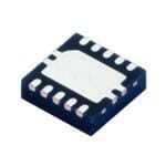
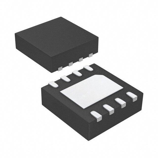
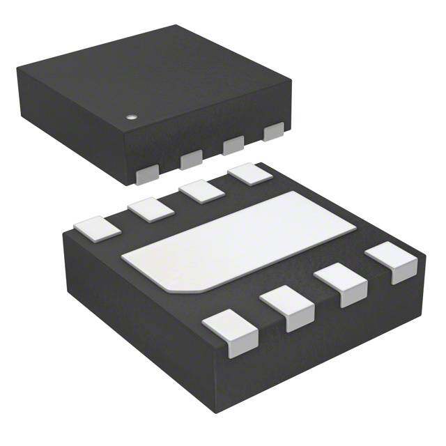
| 封装/外壳 | 10-VFDFN 裸露焊盘 |
| 封装/箱体 | VSON-10 |
| 工作温度 | -40°C ~ 85°C |
| 工作频率 | 1.2 MHz |
| 工厂包装数量 | 3000 |
| 拓扑结构 | Boost |
| 最大工作温度 | + 85 C |
| 最大电源电流 | 6 mA |
| 最小工作温度 | - 40 C |
| 标准包装 | 1 |
| 电压-输入 | 2.5 V ~ 6 V |
| 电压-输出 | 2.5 V ~ 27 V |
| 电流-输出 | 500mA |
| 类型 | 升压(升压) |
| 系列 | TPS61080 |
| 输入电压 | 2.5 V to 6 V |
| 输出数 | 1 |
| 输出电流 | 500 mA |
| 输出端数量 | 1 Output |
| 输出类型 | 可调式 |
| 配用 | /product-detail/zh/TPS61080EVM-147/296-31220-ND/1907973 |
| 频率-开关 | 600kHz,1.2MHz |


- 商务部:美国ITC正式对集成电路等产品启动337调查
- 曝三星4nm工艺存在良率问题 高通将骁龙8 Gen1或转产台积电
- 太阳诱电将投资9.5亿元在常州建新厂生产MLCC 预计2023年完工
- 英特尔发布欧洲新工厂建设计划 深化IDM 2.0 战略
- 台积电先进制程称霸业界 有大客户加持明年业绩稳了
- 达到5530亿美元!SIA预计今年全球半导体销售额将创下新高
- 英特尔拟将自动驾驶子公司Mobileye上市 估值或超500亿美元
- 三星加码芯片和SET,合并消费电子和移动部门,撤换高东真等 CEO
- 三星电子宣布重大人事变动 还合并消费电子和移动部门
- 海关总署:前11个月进口集成电路产品价值2.52万亿元 增长14.8%


PDF Datasheet 数据手册内容提取
Product Sample & Technical Tools & Support & Reference Folder Buy Documents Software Community Design TPS61080,TPS61081 SLVS644E–FEBRUARY2006–REVISEDDECEMBER2014 TPS6108x High-Voltage DC-DC Boost Converter With 0.5-A,1.3-A Integrated Switch 1 Features 3 Description • 2.5-Vto6-VInputVoltageRange The TPS6108x is a 1.2 MHz/600 kHz fixed-frequency 1 boost regulator designed for high integration, which • Upto27-VOutputVoltage integratesapowerswitch,anI/Oisolationswitch,and • 0.5-AIntegratedSwitch(TPS61080) a power diode. When a short-circuit condition is 1.3-AIntegratedSwitch(TPS61081) detected, the isolation switch opens up to disconnect • 12-V/400-mAand24-V/170-mAFrom5-VInput the output from the input. As a result, the IC protects itself and the input source from any pin, except VIN, (Typical) from being shorted to ground. The isolation switch • IntegratedPowerDiode also disconnects the output from input during • 1.2-MHz/600-kHzSelectableFixedSwitching shutdown to prevent any leakage current. Other Frequency provisions for protection include 0.5 A/1.3 A peak-to- peak overcurrent protection, programmable soft start • Input-to-OutputIsolation (SS), over voltage protection (OVP), thermal • Short-CircuitProtection shutdown,andundervoltagelockout(UVLO). • ProgrammableSoftStart The IC operates from input supplies including single • OvervoltageProtection Li-ionbattery,tripleNiMH,andregulated5V,suchas • Upto87%Efficiency USB output. The output can be boosted up to 27 V. • 10-Pin3-mm×3-mmQFNPackage TPS6108x can provide the supply voltages of OLED, TFT-LCD bias, 12-V and 24-V power rails. The output 2 Applications of TPS6108x can also be configured as a current source to power up to seven WLEDs in flash light • 3.3-Vto12-V,5-Vto12-V,and24-VBoost applications. Converter • WhiteLEDBacklightforMediaFormFactor DeviceInformation(1) Display PARTNUMBER PACKAGE BODYSIZE(NOM) • OLEDPowerSupply TPS61080 VSON(10) 3.00mm×3.00mm • xDSLApplications TPS61081 • TFT-LCDBiasSupply (1) For all available packages, see the orderable addendum at theendofthedatasheet. • WhiteLEDFlashLight 4 5-V To 12-V, 250-mA Step-Up DC-DC Converter TPS61081 L1 4.7 µH Vin 5V VIN L SW V 12 V/250 mA O EN OUT C1 R3 R1 C3 FSW 4.7mF 100Ω 437 kW 33pF SS FB 4.7µF Cs GND PGND R2 47 nF 49.9 kW L1:TDK VLCF5020T-4R7N1R7-1 C3: Feed forward capacitor for stability C1: Murata GRM188R60J105K R3: Noise decoupling resistor C2: Murata GRM219R61C475K Cs: Soft start programming capacitor 1 An IMPORTANT NOTICE at the end of this data sheet addresses availability, warranty, changes, use in safety-critical applications, intellectualpropertymattersandotherimportantdisclaimers.PRODUCTIONDATA.
TPS61080,TPS61081 SLVS644E–FEBRUARY2006–REVISEDDECEMBER2014 www.ti.com Table of Contents 1 Features.................................................................. 1 9.3 FeatureDescription.................................................10 2 Applications........................................................... 1 9.4 DeviceFunctionalModes........................................11 3 Description............................................................. 1 10 ApplicationandImplementation........................ 13 4 5-VTo12-V,250-mAStep-UpDC-DCConverter.1 10.1 ApplicationInformation..........................................13 10.2 TypicalApplication ...............................................15 5 RevisionHistory..................................................... 2 10.3 SystemExamples.................................................18 6 DeviceComparisonTable..................................... 3 11 PowerSupplyRecommendations..................... 20 7 PinConfigurationandFunctions......................... 3 12 Layout................................................................... 20 8 Specifications......................................................... 4 12.1 LayoutGuidelines.................................................20 8.1 AbsoluteMaximumRatings......................................4 12.2 LayoutExample....................................................20 8.2 ESDRatings..............................................................4 13 DeviceandDocumentationSupport................. 21 8.3 RecommendedOperatingConditions.......................4 13.1 DeviceSupport......................................................21 8.4 ThermalInformation .................................................4 13.2 RelatedLinks........................................................21 8.5 ElectricalCharacteristics..........................................5 13.3 Trademarks...........................................................21 8.6 TypicalCharacteristics..............................................6 13.4 ElectrostaticDischargeCaution............................21 9 DetailedDescription.............................................. 9 13.5 Glossary................................................................21 9.1 Overview...................................................................9 14 Mechanical,Packaging,andOrderable 9.2 FunctionalBlockDiagram.........................................9 Information........................................................... 21 5 Revision History ChangesfromRevisionD(April2013)toRevisionE Page • AddedDeviceInformationandESDRatingstables,FeatureDescriptionsection,DeviceFunctionalModes, ApplicationandImplementationsection,PowerSupplyRecommendationssection,Layoutsection,Deviceand DocumentationSupportsection,andMechanical,Packaging,andOrderableInformationsection ..................................... 1 ChangesfromRevisionC(July2011)toRevisionD Page • ChangedNote2oftheElectricalCharacteristicstable.......................................................................................................... 5 • ChangedthefirstparagraphoftheSTARTUPsection....................................................................................................... 10 ChangesfromRevisionB(January2007)toRevisionC Page • AddedaMaxvalueof30µFtoC intheRecommendedOperatingConditionsTable...................................................... 4 OUT • Addedsentence"Theoutputcapacitorvaluemustbe...."totheInputandOutputCapacitorSelectionsection................. 16 ChangesfromRevisionA(February2006)toRevisionB Page • Changedfroma1pageProductPreviewtothefulldatasheet............................................................................................. 1 ChangesfromOriginal(February2006)toRevisionA Page • ChangedtheTypicalApplicationcircuit.................................................................................................................................. 1 2 SubmitDocumentationFeedback Copyright©2006–2014,TexasInstrumentsIncorporated ProductFolderLinks:TPS61080 TPS61081
TPS61080,TPS61081 www.ti.com SLVS644E–FEBRUARY2006–REVISEDDECEMBER2014 6 Device Comparison Table OVERCURRENT PARTNUMBER(1) LIMIT 0.5-A(min) TPS61080 1.3-A(min) TPS61081 (1) ForcompleteorderableinformationseeMechanical,Packaging,andOrderableInformationattheendofthisdatasheet. 7 Pin Configuration and Functions 10-PinVSON (DRC)PackagewithThermalPad TopView L SW VIN OUT Thermal SS Pad PGND GND FSW FB EN PinFunctions PIN I/O DESCRIPTION NAME NO. Enablepin.Whenthevoltageofthispinfallsbelowenablethresholdformorethan74ms,theICturnsoff EN 6 I andconsumeslessthan2μAcurrent. Voltagefeedbackpinfortheoutputregulation.Itisregulatedtoaninternalreferencevoltage.Anexternal FB 5 I voltagedividerfromtheoutputtoGNDwiththecentertapconnectedtothispinprogramstheregulated voltage.Thispincanalsobeconnectedtoalowsidecurrentsenseresistortoprogramcurrentregulation. Switchingfrequencyselectionpin.Logichighonthepinselects1.2MHz,whilelogiclowreducesthe FSW 7 I frequencyto600kHzforbetterlightloadefficiency. GND 4 SignalgroundoftheIC TheinductorisconnectedbetweenthispinandtheSWpin.Thispinconnectstothesourceoftheisolation L 1 I FETaswell.MinimizetraceareaatthispintoreduceEMI. Outputoftheboostregulator.Whentheoutputvoltageexceedsthe27-Vovervoltageprotection(OVP) OUT 9 O threshold,thePWMswitchturnsoffuntilVoutdrops0.7Vbelowtheovervoltagethreshold. PowergroundoftheIC.ItisconnectedtothesourceofthePWMswitch.Thispinshouldbemadevery PGND 8 closetotheoutputcapacitorinlayout. SS 3 I Softstartprogrammingpin.AcapacitorbetweentheSSpinandGNDpinprogramssoftstarttiming. SW 10 I SwitchingnodeoftheIC.ConnecttheinductorbetweenthispinandtheLpin. InputpintotheIC.Itistheinputtotheboostregulator,andalsopowerstheICcircuit.Itisconnectedto VIN 2 I thedrainoftheisolationFETaswell. Thethermalpadshouldbesolderedtotheanalogground.Ifpossible,usethermalviatoconnecttoground ThermalPad – planeforidealpowerdissipation. Copyright©2006–2014,TexasInstrumentsIncorporated SubmitDocumentationFeedback 3 ProductFolderLinks:TPS61080 TPS61081
TPS61080,TPS61081 SLVS644E–FEBRUARY2006–REVISEDDECEMBER2014 www.ti.com 8 Specifications 8.1 Absolute Maximum Ratings overoperatingfree-airtemperaturerange(unlessotherwisenoted)(1) MIN MAX UNIT SupplyVoltagesonpinVIN(2) –0.3 7 V VoltagesonpinsEN,FB,SS,LandFSW(2) –0.3 7 V VoltageonpinOUT(2) 30V V VoltageonpinSW(2) 30V V ContinuousPowerDissipation SeeThermalInformation OperatingJunctionTemperatureRange –40 150 °C Storagetemperaturerange –65 150 °C (1) StressesbeyondthoselistedunderAbsoluteMaximumRatingsmaycausepermanentdamagetothedevice.Thesearestressratings only,andfunctionaloperationofthedeviceattheseoranyotherconditionsbeyondthoseindicatedunderRecommendedOperating Conditionsisnotimplied.Exposuretoabsolute-maximum-ratedconditionsforextendedperiodsmayaffectdevicereliability. (2) Allvoltagevaluesarewithrespecttonetworkgroundterminal. 8.2 ESD Ratings VALUE UNIT Human-bodymodel(HBM),perANSI/ESDA/JEDECJS-001(1) ±2000 V(ESD) Electrostaticdischarge Charged-devicemodel(CDM),perJEDECspecificationJESD22- ±750 V C101(2) (1) JEDECdocumentJEP155statesthat500-VHBMallowssafemanufacturingwithastandardESDcontrolprocess. (2) JEDECdocumentJEP157statesthat250-VCDMallowssafemanufacturingwithastandardESDcontrolprocess. 8.3 Recommended Operating Conditions overoperatingfree-airtemperaturerange(unlessotherwisenoted) MIN NOM MAX UNIT V Inputvoltagerange 2.5 6.0 V IN V Outputvoltagerange VIN 27 V OUT L Inductor(1) 4.7 10 μH C Inputcapacitor(1) 1 μF IN C Outputcapacitor(1) 4.7 30 μF OUT T Operatingambienttemperature –40 85 °C A T Operatingjunctiontemperature –40 125 °C J (1) RefertoApplicationandImplementationforfurtherinformation 8.4 Thermal Information TPS6108x THERMALMETRIC(1) DRC UNIT 10PINS R Junction-to-ambientthermalresistance 45.3 θJA R Junction-to-case(top)thermalresistance 52.2 θJC(top) R Junction-to-boardthermalresistance 20.9 θJB °C/W ψ Junction-to-topcharacterizationparameter 0.9 JT ψ Junction-to-boardcharacterizationparameter 20.7 JB R Junction-to-case(bottom)thermalresistance 5.3 θJC(bot) (1) Formoreinformationabouttraditionalandnewthermalmetrics,seetheICPackageThermalMetricsapplicationreport,SPRA953. 4 SubmitDocumentationFeedback Copyright©2006–2014,TexasInstrumentsIncorporated ProductFolderLinks:TPS61080 TPS61081
TPS61080,TPS61081 www.ti.com SLVS644E–FEBRUARY2006–REVISEDDECEMBER2014 8.5 Electrical Characteristics VIN=3.6V,EN=VIN,T =–40°Cto85°C,typicalvaluesareatT =25°C(unlessotherwisenoted) A A PARAMETER TESTCONDITIONS MIN TYP MAX UNIT SUPPLYCURRENT V Inputvoltagerange 2.5 6.0 V IN I OperatingquiescentcurrentintoVIN Deviceswitchingnoload 6 mA Q I Shutdowncurrent EN=GND 1 μA SD V Undervoltagelockoutthreshold V falling 1.65 1.8 V UVLO IN V Undervoltagelockouthysterisis 50 mV hys ENABLE Enablelevelvoltage V =2.5Vto6V 1.2 IN V V EN Disablelevelvoltage V =2.5Vto6V 0.4 IN R Enablepulldownresistor 400 800 1600 kΩ en t ENpulsewidthtodisable ENhightolow 74 ms off SOFTSTART T =25°C 4.75 5 5.25 A I Softstartbiascurrent μA ss 4.6 5 5.4 V SSpintoFBpinaccuracy V =500mV 487 500 513 mV clp SS FEEDBACKFB I Feedbackinputbiascurrent V =1.229V –100 100 nA FB FB V Feedbackregulationvoltage 1.204 1.229 1.254 V FB POWERSWITCHANDDIODE IsolationMOSFETon-resistance 0.06 0.1 Ω R V =VGS=3.6V 0.17 0.22 DS(ON) IN N-channelMOSFETon-resistance Ω V =VGS=2.5V 0.2 0.32 IN I N-channelleakagecurrent V =28V 1 2 μA LN_NFET DS V Powerdiodeforwardvoltage Id=1A 0.85 1 V F I IsolationFETleakagecurrent Lpintoground 1 μA LN_ISO OCANDSC TPS61080,FSW=HighorFSW=Low 0.5 0.7 1.0 I N-ChannelMOSFETcurrentlimit(1) A LIM TPS61081,FSW=HighorFSW=Low 1.3 1.6 2.0 TPS61080 1.0 2.2 I Shortcircuitcurrentlimit A SC TPS61081 2.0 3.5 t Shortcircuitdelaytime 13 μs scd t Shortcircuitreleasetime 57 ms scr V OUTshortdetectionthreshold (2) V –V 1.4 V SC IN OUT OSCILLATOR FSWpinhigh 1.0 1.2 1.5 f Oscillatorfrequency MHz S FSWpinlow 0.5 0.6 0.7 D Maximumdutycycle FB=1.0V 90% 94% max D Minimumdutycycle 5% min R FSWpinpulldownresistance 400 800 1600 kΩ fsw FSWhighlogic 1.6 V V FSW FSWlowlogic 0.8 (1) V =3.6V,V =15V,Dutycycle=76%.SeeFigure5toFigure8forotheroperationconditions. IN OUT (2) OUTshortcircuitconditionisdetectedifOUTstayslowerthanVIN–V for1.7msafterICenables.SeetheStartUpsectionfor SC details. Copyright©2006–2014,TexasInstrumentsIncorporated SubmitDocumentationFeedback 5 ProductFolderLinks:TPS61080 TPS61081
TPS61080,TPS61081 SLVS644E–FEBRUARY2006–REVISEDDECEMBER2014 www.ti.com Electrical Characteristics (continued) VIN=3.6V,EN=VIN,T =–40°Cto85°C,typicalvaluesareatT =25°C(unlessotherwisenoted) A A PARAMETER TESTCONDITIONS MIN TYP MAX UNIT OVP Outputovervoltageprotection V rising 27 28 29 V OUT Vovp Outputovervoltageprotectionhysteresis V falling 0.7 V OUT THERMALSHUTDOWN T Thermalshutdownthreshold 160 °C shutdown T Thermalshutdownthresholdhysteresis 15 °C hysteresis 8.6 Typical Characteristics Table1.TableOfGraphs FIGURE Efficiency V I ,VIN=3.6VOUT=12V,15V,20V,25V,FSW=HIGH,L=4.7μH Figure1 S OUT V I ,VIN=3.6VOUT=12V,15V,20V,25V,FSW=LOW,L=10μH Figure2 S OUT V I ,VIN=3V,3.6V,5V,OUT=12V,FSW=HIGH,L=4.7μH Figure3 S OUT V I ,VIN=3V,3.6V,5V,OUT=12V,FSW=LOW,L=10μH Figure4 S OUT OvercurrentLimit VIN=3.0V,3.6V,5V,FSW=High/Low Figure5, Figure6, Figure7,Figure8 LineRegulation TPS61081,VIN=2.5Vto6V,OUT=12V,I =100mA Figure9 OUT LoadRegulation TPS61081,VIN=3.6V,OUT=12V Figure10 spacer 100 100 90 90 80 80 Efficiency - % 70 VO= 25 V VO= 20 VVO= 16 V VO= 12 V Efficiency - % 70 VO= 25 VVO= 20 V VO= 16 V VO= 12 V 60 60 50 50 40 40 0 50 100 150 200 250 300 0 50 100 150 200 250 300 IO- Output Current - mA IO- Output Current - mA VI=3.6V FSW=HIGH VI=3.6V FSW=LOW Figure1.TPS61081Efficiency Figure2.TPS61081Efficiency 6 SubmitDocumentationFeedback Copyright©2006–2014,TexasInstrumentsIncorporated ProductFolderLinks:TPS61080 TPS61081
TPS61080,TPS61081 www.ti.com SLVS644E–FEBRUARY2006–REVISEDDECEMBER2014 100 100 90 90 80 80 y - % VI= 3 V VI= 3.6 V VI= 5 V % VI= 3 V VI= 5 V Efficienc 7600 Efficiency - 6700 VI= 3.6 V 50 50 40 40 30 30 0 50 100 150 200 250 300 350 0 50 100 150 200 250 300 350 IO- Output Current - mA IO- Output Current - mA V =12V FSW=HIGH V =12V FSW=LOW O O Figure3.TPS61081Efficiency Figure4.TPS61081Efficiency 1 1 VI= 3.6 V 0.8 0.8 VI= 3.6 V mit -A 0.6 VI= 3 V VI= 5 V mit -A 0.6 VI= 3 V VI= 5 V Current Li 0.4 Current Li 0.4 0.2 0.2 0 0 20 30 40 50 60 70 80 90 20 30 40 50 60 70 80 90 Duty Cycle - % Duty Cycle - % FSW=LOW FSW=HIGH Figure5.TPS61080OvercurrentLimit Figure6.TPS61080OvercurrentLimit 2 2 VI= 5 V 1.60 VI= 3 V 1.60 VI= 5 V VI= 3.6 V VI= 3 V VI= 3.6 V A A mit -1.20 mit - 1.20 Current Li0.80 Current Li 0.80 0.40 0.40 0 0 20 30 40 50 60 70 80 90 20 30 40 50 60 70 80 90 Duty Cycle - % Duty Cycle - % FSW=LOW FSW=HIGH Figure7.TPS61081OvercurrentLimit Figure8.TPS61081OvercurrentLimit Copyright©2006–2014,TexasInstrumentsIncorporated SubmitDocumentationFeedback 7 ProductFolderLinks:TPS61080 TPS61081
TPS61080,TPS61081 SLVS644E–FEBRUARY2006–REVISEDDECEMBER2014 www.ti.com 12.30 12.32 12.29 12.30 12.28 TA= 85 °C V- Output Voltage - VO 11112222....22226574 TTAA== 2 -54 0° C°C V- Output Voltage - VO 111222...222468 TATTA=A 8==5 2 -°54C 0°C °C 12.23 IO= 150 mA 12.22 VI= 3.6 V 12.22 IO= 100 mA VI= 5 V 12.21 12.20 2.5 3 3.5 4 4.5 5 5.5 6 0 0.05 0.10 0.15 0.20 0.25 0.30 VI- Input Voltage - V IO- Output Current -A Figure9.TPS61081LineRegulation Figure10.TPS61081LoadRegulation 8 SubmitDocumentationFeedback Copyright©2006–2014,TexasInstrumentsIncorporated ProductFolderLinks:TPS61080 TPS61081
TPS61080,TPS61081 www.ti.com SLVS644E–FEBRUARY2006–REVISEDDECEMBER2014 9 Detailed Description 9.1 Overview TPS6108x is a highly integrated boost regulator for up to 27-V output. In addition to the on-chip 0.5-A/1.2-A PWM switch and power diode, this IC also builds in an input side isolation switch as shown in the block diagram. One common issue with conventional boost regulator is the conduction path from input to output even when PWM switch is turned off. It creates three problems, inrush current during start up, output leakage voltage under shutdown, and unlimited short circuit current. To address these issues, TPS6108x turns off the isolation switch undershutdownmodeandshortcircuitconditiontoeliminateanypossiblecurrentpath. TPS6108x adopts current mode control with constant PWM (pulse width modulation) frequency. The switching frequency can be configured to either 600 kHz or 1.2 MHz through the FSW pin. 600 kHz improves light load efficiency, while 1.2 MHz allows using smaller external component. The PWM operation turns on the PWM switch at the beginning of each switching cycle. The input voltage is applied across the inductor and stores the energy as inductor current ramps up. The load current is provided by the output capacitor. When the inductor current across the threshold set by error amplifier output, the PWM switch is turned off, and the power diode is forward biased. The inductor transfers its stored energy to replenish the output capacitor. This operation repeats inthenextswitchingcycle. The error amplifier compares the FB pin voltage with an internal reference, and its output determines the duty cycle of the PWM switching. This close loop system requires loop compensation for stable operation. TPS6108x has internal compensation circuitry which accommodates a wide range of input and output voltages. The TPS6108x integrates slope compensation to the current ramp to avoid the sub-harmonic oscillation that is intrinsictocurrentmodecontrolschemes. 9.2 Functional Block Diagram L1 2 1 10 VIN L SW C1 Charge Pump Current Sensor EN OUT EN SC 6 OVP 9 ShortCircuit SC OVP Ramp + OVP R1 C3 Generator BandGap PWM Control SS 1.229V Oscillator 3 1.2MHz SThhuetdrmowaln C2 600KHz Clamp Cs MUX R2 R3 Error FB Amplifer FSW PGND GND FB 5 7 8 4 Copyright©2006–2014,TexasInstrumentsIncorporated SubmitDocumentationFeedback 9 ProductFolderLinks:TPS61080 TPS61081
TPS61080,TPS61081 SLVS644E–FEBRUARY2006–REVISEDDECEMBER2014 www.ti.com 9.3 Feature Description 9.3.1 StartUp TPS6108x turns on the isolation FET when the EN pin is pulled high, provided that the input voltage is higher than the undervoltage lockout threshold. The Vgs of the isolation FET is clamped to maintain high on-resistance and limits the current to 30mA charging the output capacitor. This feature limits the in-rush current and maximum startupcurrentto30mA.OncetheoutputcapacitorischargedtoVIN,theICremovestheVgsclamptofullyturn ontheisolationFETandatthesametimeactivessoftstartbychargingthecapacitorontheSSpin.IfOUTstays lower than VIN-Vsc following a 1.7ms delay after enable is taken high, the IC recognizes a short circuit condition. In this case, the isolation FET turns off, and IC remains off until the EN pin toggles or VIN cycles through power onreset(POR). During the soft start phase, the SS pin capacitor is charged by internal bias current of the SS pin. The SS pin capacitor programs the ramp up slope. The SS pin voltage clamps the reference voltage of the FB pin, therefore the output capacitor rise time follows the SS pin voltage. Without the soft start, the inductor current could reach the overcurrent limit threshold, and there is potential for output overshoot. see the Application and Implementation section on selecting soft start capacitor values. Pulling the SS pin to ground disables the PWM switching. However, unlike being disabled by pulling EN low, the IC continues to draw quiescent current and the isolationFETremainson. 9.3.2 OvercurrentandShortCircuitProtection TPS6108x has a pulse by pulse overcurrent limit feature which turns off the power switch once the inductor current reaches the overcurrent limit. The PWM circuitry resets itself at the beginning of the next switch cycle. The overcurrent threshold determines the available output current. However, the maximum output is also a function of the input voltage, output voltage, switching frequency and inductor value. Larger inductor values and 1.2MHzswitchingfrequencyincreasethecurrentoutputcapabilitybecauseofthereducedcurrentripple.Seethe APPLICATIONINFORMATIONsectionforthemaximumoutputcurrentcalculation. In typical boost converter topologies, if the output is grounded, turning off the power switch does not limit the currentbecauseacurrentpathexistsfromtheinputtooutputthroughtheinductorandpowerdiode.Toeliminate this path, TPS6108x turns off the isolation FET between the input and the inductor. This circuit is triggered when the inductor current remains above short circuit current limit for more than 13μs, or the OUT pin voltage falls belowVIN-1.4Vformorethan1.7ms.Aninternalcatch-diodebetweentheLpinandgroundturnsontoprovidea current discharge path for the inductor. If the short is caused by the output being low, then the IC shuts down and waits for EN to be toggled or a POR. If the short protection is triggered by short circuit current limit, the IC attempts to start up one time. After 57ms, the IC restarts in a fashion described in the above section. If the short is cleared, the boost regulator properly starts up and reaches output regulation. However, after reaching regulation, if another event of short circuit current limit occurs, the IC goes into shutdown mode again, and the faultcanonlybeclearedbytogglingtheENpinorPOR.Underapermanentshortcircuit,theICshutsdownafter astartupfailureandwaitsforPORortheENpintoggling. The same circuit also protects the ICs and external components when the SW pin is shorted to ground. These features provide much more comprehensive and reliable protection than the conventional boost regulator. Table2liststheICprotectionagainsttheshortofeachICpin. 10 SubmitDocumentationFeedback Copyright©2006–2014,TexasInstrumentsIncorporated ProductFolderLinks:TPS61080 TPS61081
TPS61080,TPS61081 www.ti.com SLVS644E–FEBRUARY2006–REVISEDDECEMBER2014 Feature Description (continued) Table2.TPS6108xShortCircuitProtectionMode SHORTEDTOGND FAULTDETECTION ICOPERATION HOWTOCLEARTHEFAULT ICrestartsafter57ms;Ifithappensagain, L,SW INDUCTOR>I for13μs TurnoffisolationFET thefaultcanonlybeclearedbytoggling SC ENorPOR. OUT(duringstart OUT<Vin–1.4Vfor2ms ICshutsdown ClearedbytogglingENorPOR up) OUT(afterstartup) OUT<Vin–1.4Vwithoutdelay ICshutsdown ClearedbytogglingENorPOR EN N/A ICdisabled N/A FSW N/A 600kHzswitchingfrequency N/A DisablePWMswitchingandnooutput; SS N/A N/A butstilldissipatequiescentcurrent. FB N/A OvervoltageprotectionoftheOUTpin OUTvoltagefailsbyOVPhysteresis GND,PGND,VIN N/A N/A N/A 9.3.3 OvervoltageProtection WhenTPS6108xisconfiguredasregulatedcurrentoutputasshownintheTypicalApplication section,theoutput voltage can run away if the current load is disconnected. The over voltage condition can also occur if the FB pin is shorted to the ground. To prevent the SW node and the output capacitor from exceeding the maximum voltage rating, an over voltage protection circuit turns off the boost regulator as soon as the output voltage exceeds the OVP threshold. When the output voltage falls 0.7 V below the OVP threshold, the regulator resumes the PWM switchingunlesstheoutputvoltageexceedstheOVPthreshold. 9.3.4 UndervoltageLockout(UVLO) An undervoltage lockout prevents mis-operation of the device for input voltages below 1.65 V (typical). When the input voltage is below the undervoltage threshold, the device remains off and both PWM and isolation switch are turned off, providing isolation between input and output. The undervoltage lockout threshold is set below minimum operating voltage of 2.5 V to avoid any transient VIN dip to trigger UVLO and causes converter reset. For the VIN voltage between UVLO threshold and 2.5 V, the IC still maintains its operation. However, the spec is notassured. 9.3.5 ThermalShutdown An internal thermal shutdown turns off the isolation and PWM switches when the typical junction temperature of 160°Cisexceeded.TheICrestartsifthejunctiontemperaturedropsby15°C. 9.4 Device Functional Modes 9.4.1 Enable Connecting the EN pin low turns off the power switch immediately, but keeps the isolation FET on. If the EN pin is logic low for more than 74 ms, the IC turns off the isolation FET and enters shutdown mode drawing less than 1 μA current. The enable input pin has an internal 800 kΩ pulldown resistor to disable the device when the pin is floating. 9.4.2 FrequencySelection The FSW pin can be connected to either a logic high or logic low to program the switching frequency to1.2 MHz or 600 kHz respectively. The 600 kHz switching frequency provides better efficiency because of lower switching losses. This advantage becomes more evident at light load when switching losses dominate overall losses. The higher switching frequency shrinks external component size and thus the size of power solution. High switching frequency also improves load transient response because the smaller value inductor takes less time to ramp up and down current. The other benefits of high switching frequency are lower output ripples and a higher maximum output current. Overall, it is recommended to use 1.2 MHz switching frequency unless light load efficiency is a majorconcern. Copyright©2006–2014,TexasInstrumentsIncorporated SubmitDocumentationFeedback 11 ProductFolderLinks:TPS61080 TPS61081
TPS61080,TPS61081 SLVS644E–FEBRUARY2006–REVISEDDECEMBER2014 www.ti.com Device Functional Modes (continued) The FSW pin has internal 800 kΩ pullup resistor to the VIN pin. Floating this pin programs the switching frequencyto1.2MHz. 9.4.3 MaximumandMinimumOutputCurrent The overcurrent limit in a boost converter limits the maximum input current and thus maximum input power from agiveninputvoltage.Maximumoutputpowerislessthanmaximuminputpowerduetopowerconversionlosses. Therefore, the overcurrent limit, the input voltage, the output voltage and the conversion efficiency all affect maximum current output. Because the overcurrent limit clamps the peak inductor current, the current ripple must be subtracted to derive maximum DC current. The current ripple is a function of the switching frequency, the inductorvalueandthedutycycle. 1 Ip(cid:4) L(cid:1)(cid:5) 1 (cid:2) 1 (cid:6)(cid:1)Fs Vout(cid:2)Vf(cid:3)Vin Vin (1) where Ip=inductorpeaktopeakripple L=inductorvalue Vf=powerdiodeforwardvoltage Fs=Switchingfrequency Thefollowingequationstakeintoaccountofalltheabovefactorsformaximumoutputcurrentcalculation. (cid:4) Ip(cid:5) Vin(cid:1) Ilim(cid:2) (cid:1)(cid:1) 2 Iout_max(cid:3) Vout (2) where Ilim=overcurrentlimit η=conversionefficiency To minimize the variation in the overcurrent limit threshold, the TPS6108x uses the VIN and OUT pin voltage to compensate for the variation caused by the slope compensation. However, the threshold still has some dependency on the VIN and OUT voltage. Use Figure 5 to Figure 8 to identify the typical overcurrent limit in your application,anduse25%tolerancetoaccountfortemperaturedependencyandprocessvariations. Because of the minimum duty cycle of each power switching cycle of TPS6108x, the device can lose regulation at the very light load. Use the following equations to calculate PWM duty cycle under discontinues conduction mode(DCM). Ipeak(cid:4)(cid:5)2(cid:1)Iload(cid:1)Vout(cid:2)Vf(cid:3)Vin L(cid:1)Fs Ipeak D(cid:4)L(cid:1) (cid:1)Fs Vin (3) Where Ipeak=inductorpeaktopeakrippleinDCM Iload=loadcurrent D=PWMswitchingdutycycle If the calculated duty cycle is less than 5%, minimum load should be considered to the boost output to ensure regulation.Figure20providesquickreferencetoidentifytheminimumloadrequirementsfortwoinputvoltages. 12 SubmitDocumentationFeedback Copyright©2006–2014,TexasInstrumentsIncorporated ProductFolderLinks:TPS61080 TPS61081
TPS61080,TPS61081 www.ti.com SLVS644E–FEBRUARY2006–REVISEDDECEMBER2014 10 Application and Implementation NOTE Information in the following applications sections is not part of the TI component specification, and TI does not warrant its accuracy or completeness. TI’s customers are responsible for determining suitability of components for their purposes. Customers should validateandtesttheirdesignimplementationtoconfirmsystemfunctionality. 10.1 Application Information TPS6108x is a highly integrated boost regulator for up to 27-V output with integration of a PWM switch, a power diode as well as an input side isolation switch.TPS6108x adopts current mode control with constant PWM (pulse width modulation) frequency. The switching frequency can be configured to either 600 kHz or 1.2 MHz through theFSWpin. 10.1.1 ProgramOutputVoltage OUT R1 C1 TPS61080/1 R3 C2 100W 4.7mF FB R2 Figure11. FeedForwardCapacitorConnectingWithFeedbackResistorDivider To program the output voltage, select the values of R1 and R2 (See Figure 11) according to the following equation. (cid:4) Vout (cid:5) R1(cid:3)R2(cid:1) (cid:2)1 1.229V (4) A optimum value for R2 is around 50kΩ which sets the current in the resistor divider chain to 1.229 V/50 kΩ = 24.58μA.TheoutputvoltagetolerancedependsontheV accuracyandtheresistordivider. FB 10.1.2 FeedForwardCapacitor A feed forward capacitor on the feedback divider, shown in Figure 11, improves transient response and phase margin.Thisnetworkcreatesalowfrequencyzeroandhighfrequencypoleat Fz(cid:2)2(cid:1)R11(cid:1)C1 (5) (cid:3) 1 1 (cid:4) 1 FP(cid:2) R1(cid:1)R2 2(cid:1)C1 (6) The frequency of the pole is determined by C1 and paralleled resistance of R1 and R2. For high output voltage, R1ismuchbiggerthanR2.So F (cid:1) 1 whenR1(cid:2)(cid:2) R2. P 2(cid:1)R2C1 (7) The loop gains more phase margin from this network when (Fz+Fp)/2 is placed right at crossover frequency, whichisapproximately15kHzwithrecommendedLandC.Thetypicalvalueforthezerofrequencyisbetween1 kHz to 10 kHz. For high output voltage, the zero and pole are further apart which makes the feed forward capacitor very effective. For low output voltage, the benefit of the feed forward capacitor is less visible. Table 3 gives the typical R1, R2 and the feed forward capacitor values at the certain output voltage. However, the transientresponseisnotgreatlyimprovedwhichimpliesthatthezerofrequencyistoohighorlowtoincreasethe phasemargin. Copyright©2006–2014,TexasInstrumentsIncorporated SubmitDocumentationFeedback 13 ProductFolderLinks:TPS61080 TPS61081
TPS61080,TPS61081 SLVS644E–FEBRUARY2006–REVISEDDECEMBER2014 www.ti.com Table3.RecommendedFeedForwardCapacitor ValuesWithDifferentOutputVoltage C1(Feed OutputVoltage R1 R2 Forward) 12V 437kΩ 49.9kΩ 33pF 16V 600kΩ 49.9kΩ 42pF 20V 762kΩ 49.9kΩ 56pF 25V 582kΩ 30.1kΩ 120pF The 100-Ω resistor is added to reduce noise coupling from the OUT to the FB pin through the feed forward capacitor.Withouttheresistor,theregulatormayoscillateathighoutputcurrent. 10.1.3 SoftStartCapacitor The voltage at the SS pin clamps the internal reference voltage, which allows the output voltage to ramp up slowly.Thesoftstarttimeiscalculatedas C (cid:1)1.229 t (cid:2) ss ss I ss (8) where C =softstartcapacitor ss I =softstartbiascurrent(TYP5 μA) ss 1.229Visthetypicalvalueofthereferencevoltage. During start up, input current has to be supplied to charge the output capacitor. This current is proportional to risingslopeoftheoutputvoltage,andpeakswhenoutputreachesregulation. I (cid:1)V I (cid:2)C ss out in_cout out C (cid:1)V (cid:1)(cid:1) ss in (9) Where I =additionalinputcurrentforchargingtheoutputcapacitor in_cout Themaximuminputduringsoftstartis V I (cid:3)I (cid:2) out (cid:1)I in_ss in_cout V (cid:1)(cid:1) load in (10) Output overshoot can occur if the input current at startup exceeds the inductor saturation current and/or reaches current limit because the error amplifier loses control of the voltage feedback loop. The in-rush current can also pulldown input sources, potentially causing system reset. Therefore, select C to make I stay below the ss in_ss inductorsaturationcurrent,theICovercurrentlimitandtheinput'smaximumsupplycurrent. TPS6108x can also be configured for constant current output, as shown in the typical applications. In this configuration, a current sense resistor is connected to FB pin for output current regulation. In order to reduce power loss on the sense resistor, FB pin reference voltage can be lowered by connecting a resistor to the SS pin The new reference voltage is simply the resistor value times the SS pin bias current. However, keep in mind that this reference has higher tolerance due to the tolerance of the bias current and sense resistor, and the offset of theclampcircuit.RefertothespecificationV andI tocalculatethetoleranceasfollowing. CLP SS Kref(cid:2)(cid:3)K2Vclp(cid:1)K2Iss(cid:1)K2R (11) Where K =percentagetoleranceoftheFBreferencevoltage. ref K =percentagetoleranceoftheclampcircuit. Vclp K =percentagetoleranceoftheSSpinbiascurrent. lss K =percentagetoleranceoftheSSpinresistor. R Without considering the SS pin resistor tolerance, the FB reference voltage has ±5.6% under the room temperature. 14 SubmitDocumentationFeedback Copyright©2006–2014,TexasInstrumentsIncorporated ProductFolderLinks:TPS61080 TPS61081
TPS61080,TPS61081 www.ti.com SLVS644E–FEBRUARY2006–REVISEDDECEMBER2014 10.2 Typical Application Figure12showstypicalapplicationcircuitforastep-upDC-DCconverter. TPS61081 L1 4.7 µH Vin 5V VIN L SW V 12 V/250 mA O EN OUT C1 R3 R1 C3 FSW 4.7mF 100Ω 437 kW 33pF SS FB 4.7µF Cs GND PGND R2 47 nF 49.9 kW L1:TDK VLCF5020T-4R7N1R7-1 C3: Feed forward capacitor for stability C1: Murata GRM188R60J105K R3: Noise decoupling resistor C2: Murata GRM219R61C475K Cs: Soft start programming capacitor SeeThird-PartyProductsDisclaimer. Figure12. 3.3Vto12V,80mAStep-UpDC-DCConverter 10.2.1 DesignRequirements Table4.TPS6108x12-VOutputDesignParameters DESIGNPARAMETERS VALUES InputVoltageRange 2.5Vto6V OutputVoltage 12V TransientResponse +/-250mV InputVoltageRipple +/-50mV OutputCurrent 250mA OperatingFrequency 1.2MHz 10.2.2 DetailedDesignProcedure 10.2.2.1 InductorSelection Because the selection of the inductor affects steady state operation, transient behavior and loop stability, the inductor is the most important component in power regulator design. There are three important inductor specifications, inductor value, DC resistance and saturation current. Considering inductor value alone is not enough. The inductance value of the inductor determines the inductor ripple current. It is generally recommended to set peak to peak ripple current given by Equation 4 to 30–40% of DC current. Also, the inductor value should not be beyond the range in the recommended operating conditions table. It is a good compromise of power losses and inductorsize.InductorDCcurrentcanbecalculatedas V (cid:1)I I (cid:2) out out L_DC V (cid:1)(cid:1) in (12) The internal loop compensation for PWM control is optimized for the external component shown in the typical application circuit with consideration of component tolerance. Inductor values can have ±20% tolerance with no current bias. When the inductor current approaches saturation level, its inductance can decrease 20% to 35% from the 0A value depending on how the inductor vendor defines saturation current. Using an inductor with a smallerinductancevalueforcesdiscontinuousPWMinwhichinductorcurrentrampsdowntozerobeforetheend of each switching cycle. It reduces the boost converter’s maximum output current, causes large input voltage ripple and reduces efficiency. An inductor with larger inductance reduces the gain and phase margin of the feedbackloop,possiblyresultingininstability. For these reasons, 10μH inductors are recommended for TPS61080 and 4.7μH inductors for TPS61081 for most applications.However,10μHinductorisalsosuitablefor600kHzswitchingfrequency. Copyright©2006–2014,TexasInstrumentsIncorporated SubmitDocumentationFeedback 15 ProductFolderLinks:TPS61080 TPS61081
TPS61080,TPS61081 SLVS644E–FEBRUARY2006–REVISEDDECEMBER2014 www.ti.com Regulator efficiency is dependent on the resistance of its high current path and switching losses associated with the PWM switch and power diode. Although the TPS6108x has optimized the internal switches, the overall efficiency still relies on inductor’s DC resistance (DCR); Lower DCR improves efficiency. However, there is a trade off between DCR and inductor size, and shielded inductors typically have higher DCR than unshielded ones.Table5listrecommendedinductormodels. Table5.RecommendedInductorForTPS6108x TPS61080 L DCRMAX SATURATIONCURRENT Size VENDOR (μH) (mΩ) (A) (L×W×Hmm) VLCF4018T 10 188 0.74 4.0×4.0×1.8 TDK CDRH4D16NP 10 118 0.96 4.0×4.0×1.8 Sumida LQH43CN100K 10 240 0.65 4.5×3.6×2.6 Murata TPS61081 L DCRMAX SATURATIONCURRENT Size VENDOR (μH) (mΩ) (A) (L×W×Hmm) VLCF5020T 4.7 122 1.74 5.0×5.0×2.0 TDK VLCF5014A 6.8 190 1.4 5.0×5.0×1.4 TDK CDRH4D14/HP 4.7 140 1.4 4.8×4.8×1.5 Sumida CDRH4D22/HP 10 144 1.5 5.0×5.0×2.4 Sumida 10.2.2.2 InputAndOutputCapacitorSelection The output capacitor is mainly selected to meet output ripple and loop stability requirements. This ripple voltage is related to the capacitor’s capacitance and its equivalent series resistance (ESR). Assuming a capacitor with zeroESR,theminimumcapacitanceneededforagivenripplecanbecalculatedby (cid:4)Vout(cid:2)Vin(cid:5)Iout Cout(cid:3)Vout(cid:1)Fs(cid:1)Vripple (13) V =Peaktopeakoutputripple. ripple For VIN = 3.6V, V = 20 V, and Fs = 1.2 MHz, 0.1% ripple (20mV) would require 1.0μ capacitor, however, the OUT minimum recommended output capacitor for control loop stability is 4.7 μF. The output capacitor value must be lessthan30µFtoensurethestartupcurrentchargestheoutputcapacitortotheinputvoltageinlessthan1.7ms. Forthisvalue,ceramiccapacitorsareagoodchoiceforitssize,costandavailability. TheadditionaloutputripplecomponentcausedbyESRiscalculatedusing: V (cid:2)I (cid:1)R ripple_ESR out ESR (14) Due to its low ESR, V can be neglected for ceramic capacitors, but must be considered if tantalum or ripple_ESR electrolyticcapacitorsareused. Duringaloadtransient,theoutputcapacitorattheoutputoftheboostconverterhastosupplyorabsorbtransient current before the inductor current ramps up its steady state value. Larger capacitors always help to reduce the voltage over and under shoot during a load transient. A larger capacitor also helps loop stability. Care must be taken when evaluating a ceramic capacitor’s derating under dc bias, aging and AC signal. For example, larger form factor capacitors (in 1206 size) have their self resonant frequencies in the range of the switching frequency. So the effective capacitance is significantly lower. The DC bias can also significantly reduce capacitance. Ceramic capacitors can loss as much as 50% of its capacitance at its rated voltage. Therefore, almost leave marginonvoltageratingtoensureadequatecapacitance. SeeDeviceSupportforpopularceramiccapacitorvendors. 16 SubmitDocumentationFeedback Copyright©2006–2014,TexasInstrumentsIncorporated ProductFolderLinks:TPS61080 TPS61081
TPS61080,TPS61081 www.ti.com SLVS644E–FEBRUARY2006–REVISEDDECEMBER2014 10.2.3 ApplicationCurves OUT SW 10V/div, DC 10V/div, DC SS OUT 2V/div, DC 10V/div, DC Input Current Input Current 500mA/div, DC 2A/div, DC Inductor Current L 500mA/div, DC 5V/div, DC t - Time - 4 ms/div t - Time - 10ms/div TPS61081 TPS61081 Figure13.SoftStart Figure14.VoutSCProtection OUT OUT 100 mV/div,AC 200 mV/div,AC Output Current Output Current 50 mA/div, DC 100 mA/div, DC t - Time - 400ms/div t - Time - 400ms/div TPS61080 TPS61081 Figure15.TransientResponse Figure16.TransientResponse OUT 50 mV/div,AC OUT 1 V/div, DC 27 V Offset VIN 50 mV/div,AC SW 20 V/div, DC SW 10 V/div, DC Inductor Current Inductor Current 1A/div, DC 500 mA/div, DC t - Time - 400 ns/div t - Time - 20 ns/div TPS61081 TPS61081 Figure17.InputandOutputRipple Figure18.OVP Copyright©2006–2014,TexasInstrumentsIncorporated SubmitDocumentationFeedback 17 ProductFolderLinks:TPS61080 TPS61081
TPS61080,TPS61081 SLVS644E–FEBRUARY2006–REVISEDDECEMBER2014 www.ti.com 1.50 1.4 1.2 1.20 A m nt - 1 V e ge - 0.90 Curr 0.8 FB - Volta 0.60 - Output 0.6 VI= 5 V O I 0.4 0.30 VI= 3.6 V 0.2 0 0 0 0.30 0.60 0.90 1.20 1.50 6 7 8 9 10 11 12 SS - Voltage - V VO- Output Voltage - V TPS61080 TPS61081 Figure19.SStoFBAccuracy Figure20.MinimumLoadRequirement 10.3 System Examples 10.3.1 TorchLightandFlashLight L1 4.7mH Torch light Vin3.6V TPS61081 Flash light L VIN SW C1 EN OUT 1mF C2 FSW 4.7mF SS FB R R2 SS GND PGND R1 10W 100 kW 10W ON/OFF Flash light L1:TDK VLCF5020T- 4R7N1R7-1 C1: MurataGRM188R60J105K; C2: Murata GRM219R61C475K Figure21. 50mATorchLightand100mAFlashLight 10.3.2 24VoutOutputConverter L1 4.7mH Vin 5 V TPS61081 VIN L SW 24 V/120 mA EN OUT C1 FSW R3 R1 C2 100W 555.8 kW 120pF 4.7mF SS FB C3 CS GND PGND R1 4.7mF 47nF 30 kW L1:TDK VLCF5020T- 4RN1R7-1 C1: Murata GRM188R60J475K; C3: Murata GRM55ER61H475K Figure22. 5Vto24V,120mAStep-UpDC-DCConverter 18 SubmitDocumentationFeedback Copyright©2006–2014,TexasInstrumentsIncorporated ProductFolderLinks:TPS61080 TPS61081
TPS61080,TPS61081 www.ti.com SLVS644E–FEBRUARY2006–REVISEDDECEMBER2014 System Examples (continued) 10.3.3 30WLEDsDriverinMediaFactorFormDisplay L1 4.7mH 10strings 10.5V/200mA TPS61081 Vin5V VIN L SW C1 EN OUT 4.7mF FSW C2 4.7mF R2 SS FB R1 80 kW GND PGND Rset 80 kW PWM 1W Signal L1:TDK VLCF5020T- 4R7N1R7-1 C1: MurataGRM188R60J475K; C2: Murata GRM219R61C475K Figure23. 30WLEDsDriverinMediaFactorFormDisplay 10.3.3.1 ±15VDualOutputConverter L1 -15V/30mA 10mH C2 0.1mF D1 D2 C4 Vin 5 V TPS61080 4.7mF VIN L SW 15V/30mA EN OUT C1 R1 FSW 4.7mF 560.3KW SS FB C3 Cs GND PGND R1 4.7mF 20nF 50KW L1: Sumida CDRH4D16NP-100NC C1: MurataGRM188R60J475K; C3,C4: Murata GRM219R61C475K D1,D2: ON Semiconductor MBR0520 Figure24. ±15VDualOutputConverter 10.3.3.2 Step-UpDC-DCConverterwithOutputDoubler L1 50V/50mA 4.7mH C2 1mF D1 D2 TPS61081 Vin5V R1 C4 VIN L SW 794KW 4.7mF EN OUT C3 C1 FSW 4.7mF 4.7mF SS FB Cs GND PGND R2 20nF 20KW L1:TDK VLCF5020T-4R7N1R7-1 C1: MurataGRM188R60J475K; C3: Murata GRM219R61C475K D1,D2: ON Semiconductor MBR0520 Figure25. 5Vto50V,50mAStep-UpDC-DCConverterwithOutputDoubler Copyright©2006–2014,TexasInstrumentsIncorporated SubmitDocumentationFeedback 19 ProductFolderLinks:TPS61080 TPS61081
TPS61080,TPS61081 SLVS644E–FEBRUARY2006–REVISEDDECEMBER2014 www.ti.com 11 Power Supply Recommendations The device is designed to operate from an input voltage supply range of TPS6108x's rating specification. This input supply must be well regulated. If the input supply is located more than a few inches from the converter, additional bulk capacitance may be required in addition to the ceramic bypass capacitors. An electrolytic or tantalumcapacitorwithavalueof47 μFisatypicalchoice. 12 Layout 12.1 Layout Guidelines As for all switching power supplies, the layout is an important step in the design, especially for high current and high switching frequencies. If the layout is not carefully done, the regulator could show stability problems as well as EMI problems. Therefore, use wide and short traces for high current paths and for power ground tracks. Input capacitor needs not only to be close to the VIN, but also close to the GND pin to reduce the voltage ripple seen by the IC. The L and SW pins are conveniently located on the edge of the IC, therefore the inductor can be placed close to the IC. The output capacitor needs to be placed near the load to minimize ripple and maximize transientperformance. To minimize the effects of ground noise, use a common node for all power grounds that are connected to the PGNDpin;and,adifferentoneforsignalgroundtyingtotheGNDpin.Connecttwogroundnodestogetheratthe load if possible. This allows the GND pin to be close to the output ground for good DC regulation. Any voltage differencebetweenthesetwonodeswouldbegainedupbyfeedbackdividerontheoutput.Itisalsobeneficialto have the ground of the output capacitor close to PGND because there is a large current between them. To lay outsignalground,itisrecommendedtouseshorttracesseparatedfrompowergroundtraces. 12.2 Layout Example Vin L1 Vout C2 C1 T h e Cs Parm PGND d al GND R2 R3* R1 EN FSW C3* 20 SubmitDocumentationFeedback Copyright©2006–2014,TexasInstrumentsIncorporated ProductFolderLinks:TPS61080 TPS61081
TPS61080,TPS61081 www.ti.com SLVS644E–FEBRUARY2006–REVISEDDECEMBER2014 13 Device and Documentation Support 13.1 Device Support 13.1.1 Third-PartyProductsDisclaimer TI'S PUBLICATION OF INFORMATION REGARDING THIRD-PARTY PRODUCTS OR SERVICES DOES NOT CONSTITUTE AN ENDORSEMENT REGARDING THE SUITABILITY OF SUCH PRODUCTS OR SERVICES OR A WARRANTY, REPRESENTATION OR ENDORSEMENT OF SUCH PRODUCTS OR SERVICES, EITHER ALONEORINCOMBINATIONWITHANYTIPRODUCTORSERVICE. 13.2 Related Links The table below lists quick access links. Categories include technical documents, support and community resources,toolsandsoftware,andquickaccesstosampleorbuy. Table6.RelatedLinks TECHNICAL TOOLS& SUPPORT& PARTS PRODUCTFOLDER SAMPLE&BUY DOCUMENTS SOFTWARE COMMUNITY TPS61080 Clickhere Clickhere Clickhere Clickhere Clickhere TPS61081 Clickhere Clickhere Clickhere Clickhere Clickhere 13.3 Trademarks Alltrademarksarethepropertyoftheirrespectiveowners. 13.4 Electrostatic Discharge Caution Thesedeviceshavelimitedbuilt-inESDprotection.Theleadsshouldbeshortedtogetherorthedeviceplacedinconductivefoam duringstorageorhandlingtopreventelectrostaticdamagetotheMOSgates. 13.5 Glossary SLYZ022—TIGlossary. Thisglossarylistsandexplainsterms,acronyms,anddefinitions. 14 Mechanical, Packaging, and Orderable Information The following pages include mechanical, packaging, and orderable information. This information is the most current data available for the designated devices. This data is subject to change without notice and revision of thisdocument.Forbrowser-basedversionsofthisdatasheet,refertotheleft-handnavigation. Copyright©2006–2014,TexasInstrumentsIncorporated SubmitDocumentationFeedback 21 ProductFolderLinks:TPS61080 TPS61081
PACKAGE OPTION ADDENDUM www.ti.com 24-Aug-2018 PACKAGING INFORMATION Orderable Device Status Package Type Package Pins Package Eco Plan Lead/Ball Finish MSL Peak Temp Op Temp (°C) Device Marking Samples (1) Drawing Qty (2) (6) (3) (4/5) TPS61080DRCR ACTIVE VSON DRC 10 3000 Green (RoHS CU NIPDAU Level-2-260C-1 YEAR -40 to 85 BCN & no Sb/Br) TPS61080DRCT ACTIVE VSON DRC 10 250 Green (RoHS CU NIPDAU Level-2-260C-1 YEAR -40 to 85 BCN & no Sb/Br) TPS61080DRCTG4 ACTIVE VSON DRC 10 250 Green (RoHS CU NIPDAU Level-2-260C-1 YEAR -40 to 85 BCN & no Sb/Br) TPS61081DRCR ACTIVE VSON DRC 10 3000 Green (RoHS CU NIPDAU Level-2-260C-1 YEAR -40 to 85 BCO & no Sb/Br) TPS61081DRCRG4 ACTIVE VSON DRC 10 3000 Green (RoHS CU NIPDAU Level-2-260C-1 YEAR -40 to 85 BCO & no Sb/Br) TPS61081DRCT ACTIVE VSON DRC 10 250 Green (RoHS CU NIPDAU Level-2-260C-1 YEAR -40 to 85 BCO & no Sb/Br) TPS61081DRCTG4 ACTIVE VSON DRC 10 250 Green (RoHS CU NIPDAU Level-2-260C-1 YEAR -40 to 85 BCO & no Sb/Br) (1) The marketing status values are defined as follows: ACTIVE: Product device recommended for new designs. LIFEBUY: TI has announced that the device will be discontinued, and a lifetime-buy period is in effect. NRND: Not recommended for new designs. Device is in production to support existing customers, but TI does not recommend using this part in a new design. PREVIEW: Device has been announced but is not in production. Samples may or may not be available. OBSOLETE: TI has discontinued the production of the device. (2) RoHS: TI defines "RoHS" to mean semiconductor products that are compliant with the current EU RoHS requirements for all 10 RoHS substances, including the requirement that RoHS substance do not exceed 0.1% by weight in homogeneous materials. Where designed to be soldered at high temperatures, "RoHS" products are suitable for use in specified lead-free processes. TI may reference these types of products as "Pb-Free". RoHS Exempt: TI defines "RoHS Exempt" to mean products that contain lead but are compliant with EU RoHS pursuant to a specific EU RoHS exemption. Green: TI defines "Green" to mean the content of Chlorine (Cl) and Bromine (Br) based flame retardants meet JS709B low halogen requirements of <=1000ppm threshold. Antimony trioxide based flame retardants must also meet the <=1000ppm threshold requirement. (3) MSL, Peak Temp. - The Moisture Sensitivity Level rating according to the JEDEC industry standard classifications, and peak solder temperature. (4) There may be additional marking, which relates to the logo, the lot trace code information, or the environmental category on the device. (5) Multiple Device Markings will be inside parentheses. Only one Device Marking contained in parentheses and separated by a "~" will appear on a device. If a line is indented then it is a continuation of the previous line and the two combined represent the entire Device Marking for that device. Addendum-Page 1
PACKAGE OPTION ADDENDUM www.ti.com 24-Aug-2018 (6) Lead/Ball Finish - Orderable Devices may have multiple material finish options. Finish options are separated by a vertical ruled line. Lead/Ball Finish values may wrap to two lines if the finish value exceeds the maximum column width. Important Information and Disclaimer:The information provided on this page represents TI's knowledge and belief as of the date that it is provided. TI bases its knowledge and belief on information provided by third parties, and makes no representation or warranty as to the accuracy of such information. Efforts are underway to better integrate information from third parties. TI has taken and continues to take reasonable steps to provide representative and accurate information but may not have conducted destructive testing or chemical analysis on incoming materials and chemicals. TI and TI suppliers consider certain information to be proprietary, and thus CAS numbers and other limited information may not be available for release. In no event shall TI's liability arising out of such information exceed the total purchase price of the TI part(s) at issue in this document sold by TI to Customer on an annual basis. Addendum-Page 2
PACKAGE MATERIALS INFORMATION www.ti.com 9-Oct-2014 TAPE AND REEL INFORMATION *Alldimensionsarenominal Device Package Package Pins SPQ Reel Reel A0 B0 K0 P1 W Pin1 Type Drawing Diameter Width (mm) (mm) (mm) (mm) (mm) Quadrant (mm) W1(mm) TPS61080DRCR VSON DRC 10 3000 330.0 12.4 3.3 3.3 1.1 8.0 12.0 Q2 TPS61080DRCT VSON DRC 10 250 180.0 12.4 3.3 3.3 1.1 8.0 12.0 Q2 TPS61081DRCR VSON DRC 10 3000 330.0 12.4 3.3 3.3 1.1 8.0 12.0 Q2 TPS61081DRCT VSON DRC 10 250 180.0 12.4 3.3 3.3 1.1 8.0 12.0 Q2 PackMaterials-Page1
PACKAGE MATERIALS INFORMATION www.ti.com 9-Oct-2014 *Alldimensionsarenominal Device PackageType PackageDrawing Pins SPQ Length(mm) Width(mm) Height(mm) TPS61080DRCR VSON DRC 10 3000 367.0 367.0 35.0 TPS61080DRCT VSON DRC 10 250 210.0 185.0 35.0 TPS61081DRCR VSON DRC 10 3000 367.0 367.0 35.0 TPS61081DRCT VSON DRC 10 250 210.0 185.0 35.0 PackMaterials-Page2
GENERIC PACKAGE VIEW DRC 10 VSON - 1 mm max height PLASTIC SMALL OUTLINE - NO LEAD Images above are just a representation of the package family, actual package may vary. Refer to the product data sheet for package details. 4204102-3/M
PACKAGE OUTLINE DRC0010J VSON - 1 mm max height SCALE 4.000 PLASTIC SMALL OUTLINE - NO LEAD 3.1 B A 2.9 PIN 1 INDEX AREA 3.1 2.9 1.0 C 0.8 SEATING PLANE 0.05 0.00 0.08 C 1.65 0.1 2X (0.5) (0.2) TYP EXPOSED 4X (0.25) THERMAL PAD 5 6 2X 11 SYMM 2 2.4 0.1 10 1 8X 0.5 0.30 10X 0.18 PIN 1 ID SYMM 0.1 C A B (OPTIONAL) 0.5 0.05 C 10X 0.3 4218878/B 07/2018 NOTES: 1. All linear dimensions are in millimeters. Any dimensions in parenthesis are for reference only. Dimensioning and tolerancing per ASME Y14.5M. 2. This drawing is subject to change without notice. 3. The package thermal pad must be soldered to the printed circuit board for optimal thermal and mechanical performance. www.ti.com
EXAMPLE BOARD LAYOUT DRC0010J VSON - 1 mm max height PLASTIC SMALL OUTLINE - NO LEAD (1.65) (0.5) 10X (0.6) 1 10 10X (0.24) 11 SYMM (2.4) (3.4) (0.95) 8X (0.5) 6 5 (R0.05) TYP ( 0.2) VIA TYP (0.25) (0.575) SYMM (2.8) LAND PATTERN EXAMPLE EXPOSED METAL SHOWN SCALE:20X 0.07 MIN 0.07 MAX EXPOSED METAL ALL AROUND ALL AROUND EXPOSED METAL SOLDER MASK METAL METAL UNDER SOLDER MASK OPENING SOLDER MASK OPENING NON SOLDER MASK SOLDER MASK DEFINED DEFINED (PREFERRED) SOLDER MASK DETAILS 4218878/B 07/2018 NOTES: (continued) 4. This package is designed to be soldered to a thermal pad on the board. For more information, see Texas Instruments literature number SLUA271 (www.ti.com/lit/slua271). 5. Vias are optional depending on application, refer to device data sheet. If any vias are implemented, refer to their locations shown on this view. It is recommended that vias under paste be filled, plugged or tented. www.ti.com
EXAMPLE STENCIL DESIGN DRC0010J VSON - 1 mm max height PLASTIC SMALL OUTLINE - NO LEAD 2X (1.5) (0.5) SYMM EXPOSED METAL 11 TYP 10X (0.6) 1 10 (1.53) 10X (0.24) 2X (1.06) SYMM (0.63) 8X (0.5) 6 5 (R0.05) TYP 4X (0.34) 4X (0.25) (2.8) SOLDER PASTE EXAMPLE BASED ON 0.125 mm THICK STENCIL EXPOSED PAD 11: 80% PRINTED SOLDER COVERAGE BY AREA SCALE:25X 4218878/B 07/2018 NOTES: (continued) 6. Laser cutting apertures with trapezoidal walls and rounded corners may offer better paste release. IPC-7525 may have alternate design recommendations. www.ti.com
IMPORTANTNOTICE TexasInstrumentsIncorporated(TI)reservestherighttomakecorrections,enhancements,improvementsandotherchangestoits semiconductorproductsandservicesperJESD46,latestissue,andtodiscontinueanyproductorserviceperJESD48,latestissue.Buyers shouldobtainthelatestrelevantinformationbeforeplacingordersandshouldverifythatsuchinformationiscurrentandcomplete. TI’spublishedtermsofsaleforsemiconductorproducts(http://www.ti.com/sc/docs/stdterms.htm)applytothesaleofpackagedintegrated circuitproductsthatTIhasqualifiedandreleasedtomarket.AdditionaltermsmayapplytotheuseorsaleofothertypesofTIproductsand services. ReproductionofsignificantportionsofTIinformationinTIdatasheetsispermissibleonlyifreproductioniswithoutalterationandis accompaniedbyallassociatedwarranties,conditions,limitations,andnotices.TIisnotresponsibleorliableforsuchreproduced documentation.Informationofthirdpartiesmaybesubjecttoadditionalrestrictions.ResaleofTIproductsorserviceswithstatements differentfromorbeyondtheparametersstatedbyTIforthatproductorservicevoidsallexpressandanyimpliedwarrantiesforthe associatedTIproductorserviceandisanunfairanddeceptivebusinesspractice.TIisnotresponsibleorliableforanysuchstatements. BuyersandotherswhoaredevelopingsystemsthatincorporateTIproducts(collectively,“Designers”)understandandagreethatDesigners remainresponsibleforusingtheirindependentanalysis,evaluationandjudgmentindesigningtheirapplicationsandthatDesignershave fullandexclusiveresponsibilitytoassurethesafetyofDesigners'applicationsandcomplianceoftheirapplications(andofallTIproducts usedinorforDesigners’applications)withallapplicableregulations,lawsandotherapplicablerequirements.Designerrepresentsthat,with respecttotheirapplications,Designerhasallthenecessaryexpertisetocreateandimplementsafeguardsthat(1)anticipatedangerous consequencesoffailures,(2)monitorfailuresandtheirconsequences,and(3)lessenthelikelihoodoffailuresthatmightcauseharmand takeappropriateactions.DesigneragreesthatpriortousingordistributinganyapplicationsthatincludeTIproducts,Designerwill thoroughlytestsuchapplicationsandthefunctionalityofsuchTIproductsasusedinsuchapplications. TI’sprovisionoftechnical,applicationorotherdesignadvice,qualitycharacterization,reliabilitydataorotherservicesorinformation, including,butnotlimitedto,referencedesignsandmaterialsrelatingtoevaluationmodules,(collectively,“TIResources”)areintendedto assistdesignerswhoaredevelopingapplicationsthatincorporateTIproducts;bydownloading,accessingorusingTIResourcesinany way,Designer(individuallyor,ifDesignerisactingonbehalfofacompany,Designer’scompany)agreestouseanyparticularTIResource solelyforthispurposeandsubjecttothetermsofthisNotice. TI’sprovisionofTIResourcesdoesnotexpandorotherwisealterTI’sapplicablepublishedwarrantiesorwarrantydisclaimersforTI products,andnoadditionalobligationsorliabilitiesarisefromTIprovidingsuchTIResources.TIreservestherighttomakecorrections, enhancements,improvementsandotherchangestoitsTIResources.TIhasnotconductedanytestingotherthanthatspecifically describedinthepublisheddocumentationforaparticularTIResource. Designerisauthorizedtouse,copyandmodifyanyindividualTIResourceonlyinconnectionwiththedevelopmentofapplicationsthat includetheTIproduct(s)identifiedinsuchTIResource.NOOTHERLICENSE,EXPRESSORIMPLIED,BYESTOPPELOROTHERWISE TOANYOTHERTIINTELLECTUALPROPERTYRIGHT,ANDNOLICENSETOANYTECHNOLOGYORINTELLECTUALPROPERTY RIGHTOFTIORANYTHIRDPARTYISGRANTEDHEREIN,includingbutnotlimitedtoanypatentright,copyright,maskworkright,or otherintellectualpropertyrightrelatingtoanycombination,machine,orprocessinwhichTIproductsorservicesareused.Information regardingorreferencingthird-partyproductsorservicesdoesnotconstitutealicensetousesuchproductsorservices,orawarrantyor endorsementthereof.UseofTIResourcesmayrequirealicensefromathirdpartyunderthepatentsorotherintellectualpropertyofthe thirdparty,oralicensefromTIunderthepatentsorotherintellectualpropertyofTI. TIRESOURCESAREPROVIDED“ASIS”ANDWITHALLFAULTS.TIDISCLAIMSALLOTHERWARRANTIESOR REPRESENTATIONS,EXPRESSORIMPLIED,REGARDINGRESOURCESORUSETHEREOF,INCLUDINGBUTNOTLIMITEDTO ACCURACYORCOMPLETENESS,TITLE,ANYEPIDEMICFAILUREWARRANTYANDANYIMPLIEDWARRANTIESOF MERCHANTABILITY,FITNESSFORAPARTICULARPURPOSE,ANDNON-INFRINGEMENTOFANYTHIRDPARTYINTELLECTUAL PROPERTYRIGHTS.TISHALLNOTBELIABLEFORANDSHALLNOTDEFENDORINDEMNIFYDESIGNERAGAINSTANYCLAIM, INCLUDINGBUTNOTLIMITEDTOANYINFRINGEMENTCLAIMTHATRELATESTOORISBASEDONANYCOMBINATIONOF PRODUCTSEVENIFDESCRIBEDINTIRESOURCESOROTHERWISE.INNOEVENTSHALLTIBELIABLEFORANYACTUAL, DIRECT,SPECIAL,COLLATERAL,INDIRECT,PUNITIVE,INCIDENTAL,CONSEQUENTIALOREXEMPLARYDAMAGESIN CONNECTIONWITHORARISINGOUTOFTIRESOURCESORUSETHEREOF,ANDREGARDLESSOFWHETHERTIHASBEEN ADVISEDOFTHEPOSSIBILITYOFSUCHDAMAGES. UnlessTIhasexplicitlydesignatedanindividualproductasmeetingtherequirementsofaparticularindustrystandard(e.g.,ISO/TS16949 andISO26262),TIisnotresponsibleforanyfailuretomeetsuchindustrystandardrequirements. WhereTIspecificallypromotesproductsasfacilitatingfunctionalsafetyorascompliantwithindustryfunctionalsafetystandards,such productsareintendedtohelpenablecustomerstodesignandcreatetheirownapplicationsthatmeetapplicablefunctionalsafetystandards andrequirements.Usingproductsinanapplicationdoesnotbyitselfestablishanysafetyfeaturesintheapplication.Designersmust ensurecompliancewithsafety-relatedrequirementsandstandardsapplicabletotheirapplications.DesignermaynotuseanyTIproductsin life-criticalmedicalequipmentunlessauthorizedofficersofthepartieshaveexecutedaspecialcontractspecificallygoverningsuchuse. Life-criticalmedicalequipmentismedicalequipmentwherefailureofsuchequipmentwouldcauseseriousbodilyinjuryordeath(e.g.,life support,pacemakers,defibrillators,heartpumps,neurostimulators,andimplantables).Suchequipmentincludes,withoutlimitation,all medicaldevicesidentifiedbytheU.S.FoodandDrugAdministrationasClassIIIdevicesandequivalentclassificationsoutsidetheU.S. TImayexpresslydesignatecertainproductsascompletingaparticularqualification(e.g.,Q100,MilitaryGrade,orEnhancedProduct). Designersagreethatithasthenecessaryexpertisetoselecttheproductwiththeappropriatequalificationdesignationfortheirapplications andthatproperproductselectionisatDesigners’ownrisk.Designersaresolelyresponsibleforcompliancewithalllegalandregulatory requirementsinconnectionwithsuchselection. DesignerwillfullyindemnifyTIanditsrepresentativesagainstanydamages,costs,losses,and/orliabilitiesarisingoutofDesigner’snon- compliancewiththetermsandprovisionsofthisNotice. MailingAddress:TexasInstruments,PostOfficeBox655303,Dallas,Texas75265 Copyright©2018,TexasInstrumentsIncorporated