ICGOO在线商城 > 集成电路(IC) > PMIC - 稳压器 - DC DC 开关稳压器 > LM5009ASD/NOPB

 Datasheet下载
- 型号: LM5009ASD/NOPB
- 制造商: Texas Instruments
- 库位|库存: xxxx|xxxx
- 要求:
| 数量阶梯 | 香港交货 | 国内含税 |
| +xxxx | $xxxx | ¥xxxx |
查看当月历史价格
查看今年历史价格
LM5009ASD/NOPB产品简介:
ICGOO电子元器件商城为您提供LM5009ASD/NOPB由Texas Instruments设计生产,在icgoo商城现货销售,并且可以通过原厂、代理商等渠道进行代购。 LM5009ASD/NOPB价格参考。Texas InstrumentsLM5009ASD/NOPB封装/规格:PMIC - 稳压器 - DC DC 开关稳压器, 可调式 降压 开关稳压器 IC 正 2.5V 1 输出 150mA 8-WDFN 裸露焊盘。您可以下载LM5009ASD/NOPB参考资料、Datasheet数据手册功能说明书,资料中有LM5009ASD/NOPB 详细功能的应用电路图电压和使用方法及教程。
Texas Instruments的LM5009ASD/NOPB是一款DC-DC开关稳压器,广泛应用于需要高效电源管理的场景。其主要应用场景包括:

1. 工业自动化:在工业控制系统中,如PLC(可编程逻辑控制器)、传感器和执行器等设备中,LM5009ASD/NOPB可以提供稳定的电源输出,确保系统的可靠性和稳定性。它能够承受恶劣的工作环境,如高温、高湿度和电磁干扰。

2. 通信设备:适用于基站、路由器和交换机等通信基础设施。这些设备通常需要长时间稳定运行,并且对电源效率要求较高。LM5009ASD/NOPB可以在宽输入电压范围内工作,适应不同的电源输入条件,同时保持高效的电源转换。

3. 汽车电子:在汽车行业中,该器件可用于车载信息娱乐系统、ADAS(高级驾驶辅助系统)和其他车载电子模块。它具有良好的抗噪性能和瞬态响应能力,能够在汽车启动时的电压波动下保持稳定输出。

4. 消费电子产品:如笔记本电脑、平板电脑和智能手机的充电器和适配器中,LM5009ASD/NOPB可以实现高效的小型化设计,减少发热并延长电池寿命。它还支持多种保护功能,如过流保护、过温保护等,提高产品的安全性。

5. 医疗设备:在便携式医疗设备如血糖仪、血压计等中,LM5009ASD/NOPB可以提供精确的电源管理,确保测量结果的准确性。它的小尺寸和低功耗特性使得它可以集成到紧凑的设计中。

6. 物联网(IoT)设备:在智能家居、智能城市等物联网应用中,LM5009ASD/NOPB可以为各种传感器节点和网关提供稳定的电源支持,确保数据传输的可靠性和设备的长续航能力。

总之,LM5009ASD/NOPB凭借其高效能、高可靠性以及广泛的适用性,成为众多领域中不可或缺的电源管理解决方案。
| 参数 | 数值 |
| 产品目录 | 集成电路 (IC)半导体 |
| 描述 | IC REG BUCK ADJ 0.15A 8LLP稳压器—开关式稳压器 100V 150mA Constant Buck Switch Reg |
| 产品分类 | |
| 品牌 | Texas Instruments |
| 产品手册 | |
| 产品图片 |
|
| rohs | 符合RoHS无铅 / 符合限制有害物质指令(RoHS)规范要求 |
| 产品系列 | 电源管理 IC,稳压器—开关式稳压器,Texas Instruments LM5009ASD/NOPB- |
| 数据手册 | |
| 产品型号 | LM5009ASD/NOPB |
| PWM类型 | - |
| 产品培训模块 | http://www.digikey.cn/PTM/IndividualPTM.page?site=cn&lang=zhs&ptm=30145http://www.digikey.cn/PTM/IndividualPTM.page?site=cn&lang=zhs&ptm=25875 |
| 产品目录页面 | |
| 产品种类 | 稳压器—开关式稳压器 |
| 供应商器件封装 | 8-LLP-EP(4x4) |
| 其它名称 | *LM5009ASD/NOPB |
| 制造商产品页 | http://www.ti.com/general/docs/suppproductinfo.tsp?distId=10&orderablePartNumber=LM5009ASD/NOPB |
| 包装 | 剪切带 (CT) |
| 同步整流器 | 无 |
| 商标 | Texas Instruments |
| 安装类型 | 表面贴装 |
| 安装风格 | SMD/SMT |
| 封装 | Reel |
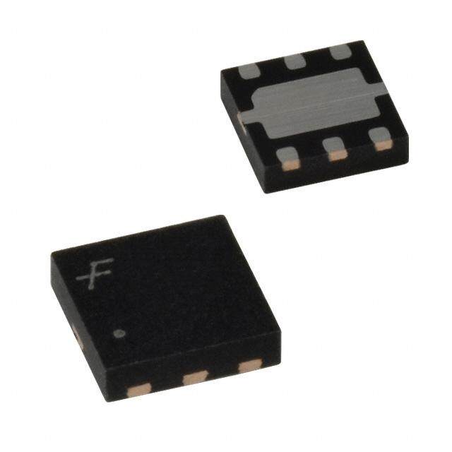
| 封装/外壳 | 8-WDFN 裸露焊盘 |
| 封装/箱体 | WSON-8 |
| 工作温度 | -40°C ~ 125°C |
| 工作温度范围 | - 40 C to + 125 C |
| 工厂包装数量 | 1000 |
| 开关频率 | 600 kHz |
| 拓扑结构 | Buck |
| 最大工作温度 | + 125 C |
| 最大输入电压 | 95 V |
| 最小工作温度 | - 40 C |
| 最小输入电压 | 6 V |
| 标准包装 | 1 |
| 电压-输入 | 6 V ~ 95 V |
| 电压-输出 | 2.5 V ~ 85 V |
| 电流-输出 | 150mA |
| 电源电压-最小 | 6 V |
| 类型 | Step Down |
| 系列 | LM5009A |
| 设计资源 | http://www.digikey.com/product-highlights/cn/zh/texas-instruments-webench-design-center/3176 |
| 输出数 | 1 |
| 输出电压 | 2.5 V to 85 V |
| 输出电流 | 150 mA |
| 输出端数量 | 1 Output |
| 输出类型 | 可调式 |
| 配用 | /product-detail/zh/LM5009AEVAL%2FNOPB/LM5009AEVAL%2FNOPB-ND/2506776 |
| 频率-开关 | 50kHz ~ 1.1MHz |


- 商务部:美国ITC正式对集成电路等产品启动337调查
- 曝三星4nm工艺存在良率问题 高通将骁龙8 Gen1或转产台积电
- 太阳诱电将投资9.5亿元在常州建新厂生产MLCC 预计2023年完工
- 英特尔发布欧洲新工厂建设计划 深化IDM 2.0 战略
- 台积电先进制程称霸业界 有大客户加持明年业绩稳了
- 达到5530亿美元!SIA预计今年全球半导体销售额将创下新高
- 英特尔拟将自动驾驶子公司Mobileye上市 估值或超500亿美元
- 三星加码芯片和SET,合并消费电子和移动部门,撤换高东真等 CEO
- 三星电子宣布重大人事变动 还合并消费电子和移动部门
- 海关总署:前11个月进口集成电路产品价值2.52万亿元 增长14.8%


PDF Datasheet 数据手册内容提取
Product Sample & Technical Tools & Support & Folder Buy Documents Software Community LM5009A SNVS608H–JUNE2009–REVISEDSEPTEMBER2016 LM5009A 100-V, 150-mA Constant ON-Time Buck Switching Regulator 1 Features 3 Description • OperatingInputVoltageRange:6Vto95V The LM5009A is a functional variant of the LM5009 1 COT buck switching regulator. The functional • Integrated100-V,N-ChannelBuckSwitch differences of the LM5009A are: The minimum input • InternalStart-UpRegulator operating voltage is 6 V, the ON-time equation is • NoLoopCompensationRequired slightly different, and the requirement for a minimum loadcurrentisremoved. • Ultra-FastTransientResponse • ONTimeVariesInverselyWithInputVoltage The LM5009A step-down switching regulator features all of the functions required to implement a low cost, • OperatingFrequencyRemainsConstantWith efficient, buck bias regulator. This high voltage VaryingLineVoltageandLoadCurrent regulator contains an 100-V N-channel buck switch. • AdjustableOutputVoltageFrom2.5V The device is easy to implement and is provided in • HighlyEfficientOperation the 8-pin VSSOP and the thermally enhanced 8-pin WSON packages. The regulator is based on a control • PrecisionInternalReference scheme using an ON time inversely proportional to • LowBiasCurrent V . This feature allows the operating frequency to IN • IntelligentCurrentLimit remain relatively constant. The control scheme requires no loop compensation. An intelligent current • ThermalShutdown limit is implemented with forced OFF time, which is • 8-PinVSSOPand8-PinWSON(4mm × 4mm) inversely proportional to V . This scheme ensures OUT Packages short-circuit control while providing minimum foldback. Other features include: thermal shutdown, 2 Applications undervoltage lockout (V ), gate drive undervoltage CC lockout, max duty cycle limiter, and a precharge • Non-IsolatedTelecommunicationBuckRegulator switch. • SecondaryHigh-VoltagePostRegulator • 42-VAutomotiveSystems DeviceInformation(1) PARTNUMBER PACKAGE BODYSIZE(NOM) VSSOP(8) 4.00mm×4.00mm LM5009A WSON(8) 4.00mm×4.00mm (1) For all available packages, see the orderable addendum at theendofthedatasheet. TypicalApplication,BasicStep-DownRegulator 6V - 95V Input VIN C1 VIN VCC C3 LM5009A RT BST GND C4 L1 RT/SD SW VOUT RCL D1 SHUTDOWN RCL RFB2 R3 RTN FB C2 GND RFB1 Copyright © 2016, Texas Instruments Incorporated 1 An IMPORTANT NOTICE at the end of this data sheet addresses availability, warranty, changes, use in safety-critical applications, intellectualpropertymattersandotherimportantdisclaimers.PRODUCTIONDATA.
LM5009A SNVS608H–JUNE2009–REVISEDSEPTEMBER2016 www.ti.com Table of Contents 1 Features.................................................................. 1 7.4 DeviceFunctionalModes........................................12 2 Applications........................................................... 1 8 ApplicationandImplementation........................ 13 3 Description............................................................. 1 8.1 ApplicationInformation............................................13 4 RevisionHistory..................................................... 2 8.2 TypicalApplication..................................................13 5 PinConfigurationandFunctions......................... 3 9 PowerSupplyRecommendations...................... 18 6 Specifications......................................................... 4 10 Layout................................................................... 18 6.1 AbsoluteMaximumRatings......................................4 10.1 LayoutGuidelines.................................................18 6.2 ESDRatings..............................................................4 10.2 LayoutExample....................................................18 6.3 RecommendedOperatingConditions.......................4 11 DeviceandDocumentationSupport................. 19 6.4 ThermalInformation..................................................4 11.1 DocumentationSupport........................................19 6.5 ElectricalCharacteristics...........................................5 11.2 ReceivingNotificationofDocumentationUpdates19 6.6 SwitchingCharacteristics..........................................6 11.3 CommunityResources..........................................19 6.7 TypicalCharacteristics..............................................7 11.4 Trademarks...........................................................19 7 DetailedDescription.............................................. 8 11.5 ElectrostaticDischargeCaution............................19 7.1 Overview...................................................................8 11.6 Glossary................................................................19 7.2 FunctionalBlockDiagram.........................................8 12 Mechanical,Packaging,andOrderable Information........................................................... 19 7.3 FeatureDescription...................................................8 4 Revision History NOTE:Pagenumbersforpreviousrevisionsmaydifferfrompagenumbersinthecurrentversion. ChangesfromRevisionG(February2013)toRevisionH Page • AddedESDRatingstable,FeatureDescriptionsection,DeviceFunctionalModes,ApplicationandImplementation section,PowerSupplyRecommendationssection,Layoutsection,DeviceandDocumentationSupportsection,and Mechanical,Packaging,andOrderableInformationsection.................................................................................................. 1 • ChangedvaluesintheThermalInformationtablefrom200to157.7(DGK)andfrom40to42.8(NGU)............................. 4 ChangesfromRevisionF(February2013)toRevisionG Page • ChangedlayoutofNationalSemiconductorDataSheettoTIformat.................................................................................... 1 2 SubmitDocumentationFeedback Copyright©2009–2016,TexasInstrumentsIncorporated ProductFolderLinks:LM5009A
LM5009A www.ti.com SNVS608H–JUNE2009–REVISEDSEPTEMBER2016 5 Pin Configuration and Functions DGKPackage 8-PinVSSOP NGUPackage TopView 8-PinWSON TopView SW 1 8 VIN BST 2 7 VCC SW 1 8 VIN RCL 3 6 RT /SD BST 2 EP 7 VCC RTN 4 5 FB RCL 3 6 RT /SD RTN 4 5 FB Not to scale Not to scale PinFunctions PIN I/O DESCRIPTION NAME NO. Switchingnode:powerswitchingnode.Connecttotheoutputinductor,recirculatingdiode,and SW 1 O bootstrapcapacitor. Boostpin(bootstrapcapacitorinput):anexternalcapacitorisrequiredbetweentheBSTandtheSW BST 2 I pins.A0.01-µFceramiccapacitorisrecommended.AninternaldiodechargesthecapacitorfromV CC duringeachOFFtime. CurrentlimitOFF-timesetpin:aresistorbetweenthispinandRTNsetstheOFFtimewhencurrentlimit RCL 3 I isdetected.TheOFFtimeispresetto35µsifFB=0V. RTN 4 — Groundpin:groundfortheentirecircuit. Feedbackinputfromregulatedoutput:thispinisconnectedtotheinvertinginputoftheinternal FB 5 I regulationcomparator.Theregulationthresholdis2.5V. Ontimesetpin:aresistorbetweenthispinandV setstheswitchontimeasafunctionofV .The IN IN R /SD 6 I minimumrecommendedontimeis400nsatthemaximuminputvoltage.Thispinisusedforremote T shutdown. Outputfromtheinternalhighvoltageseriespassregulator:thisregulatedvoltageprovidesgatedrive V 7 O powerfortheinternalBuckswitch.AninternaldiodeisprovidedbetweenthispinandtheBSTpin.A CC local0.47-µFdecouplingcapacitorisrequired.Theseriespassregulatoriscurrentlimitedto9mA. V 8 I Inputvoltage:inputoperatingrangeof6Vto95V. IN Exposedpad:theexposedpadhasnoelectricalcontact.Connecttosystemgroundplaneforreduced EP — — thermalresistance. Copyright©2009–2016,TexasInstrumentsIncorporated SubmitDocumentationFeedback 3 ProductFolderLinks:LM5009A
LM5009A SNVS608H–JUNE2009–REVISEDSEPTEMBER2016 www.ti.com 6 Specifications 6.1 Absolute Maximum Ratings overoperatingfree-airtemperaturerange(unlessotherwisenoted)(1) MIN MAX UNIT V toGND –0.3 100 V IN BSTtoGND –0.3 114 V SWtoGND(steadystate) –1 V BSTtoV 100 V CC BSTtoSW 14 V V toGND 14 V CC AllotherinputstoGND –0.3 7 V Storagetemperature,T –55 150 °C stg (1) StressesbeyondthoselistedunderAbsoluteMaximumRatingsmaycausepermanentdamagetothedevice.Thesearestressratings only,whichdonotimplyfunctionaloperationofthedeviceattheseoranyotherconditionsbeyondthoseindicatedunderRecommended OperatingConditions.Exposuretoabsolute-maximum-ratedconditionsforextendedperiodsmayaffectdevicereliability. 6.2 ESD Ratings VALUE UNIT Human-bodymodel(HBM),perANSI/ESDA/JEDECJS-001(1) ±2000 V Electrostaticdischarge V (ESD) Charged-devicemodel(CDM),perJEDECspecificationJESD22-C101(2) ±750 (1) JEDECdocumentJEP155statesthat500-VHBMallowssafemanufacturingwithastandardESDcontrolprocess. (2) JEDECdocumentJEP157statesthat250-VCDMallowssafemanufacturingwithastandardESDcontrolprocess. 6.3 Recommended Operating Conditions overoperatingfree-airtemperaturerange(unlessotherwisenoted) MIN MAX UNIT V Inputvoltage 6 95 V IN T Operatingjunctiontemperature –40 125 °C J 6.4 Thermal Information LM5009A THERMALMETRIC(1) DGK(VSSOP) NGU(WSON) UNIT 8PINS 8PINS R Junction-to-ambientthermalresistance 157.7 42.8 °C/W θJA R Junction-to-case(top)thermalresistance 50.2 41.5 °C/W θJC(top) R Junction-to-boardthermalresistance 77.9 20.1 °C/W θJB ψ Junction-to-topcharacterizationparameter 4.5 0.4 °C/W JT ψ Junction-to-boardcharacterizationparameter 76.5 20.2 °C/W JB R Junction-to-case(bottom)thermalresistance — 4.5 °C/W θJC(bot) (1) Formoreinformationabouttraditionalandnewthermalmetrics,seetheSemiconductorandICPackageThermalMetricsapplication report. 4 SubmitDocumentationFeedback Copyright©2009–2016,TexasInstrumentsIncorporated ProductFolderLinks:LM5009A
LM5009A www.ti.com SNVS608H–JUNE2009–REVISEDSEPTEMBER2016 6.5 Electrical Characteristics TypicalvaluescorrespondtoT =25°C.MinimumandmaximumlimitsapplyoverT =–40°Cto125°CforLM5009A.Unless J J otherwisestated,V =48V(1) IN PARAMETER TESTCONDITIONS MIN TYP MAX UNIT V SUPPLY CC V Reg V regulatoroutput(2) V =48V 6.6 7 7.4 V CC CC IN V –V 6V<V <8.5V 100 mV IN CC IN V bypassthreshold V increasing 8.5 V CC IN V bypasshysteresis 300 mV CC V =6V 100 Ω IN V outputimpedance V =10V 8.8 Ω CC IN V =48V 0.8 Ω IN V currentlimit V =48V 9.2 mA CC IN V UVLO V increasing 5.3 V CC CC V UVLOhysteresis 190 mV CC V UVLOfilterdelay 3 µs CC Iinoperatingcurrent FB=3V,V =48V 550 750 µA IN Iinshutdowncurrent R /SD=0V 110 176 µA T CURRENTLIMIT Currentlimitthreshold 0.24 0.3 0.36 A Currentlimitresponsetime I overdrive=0.1A,timetoswitchoff 350 ns switch T OFF-timegenerator FB=0V,R =100K 35 µs OFF-1 CL T OFF-timegenerator FB=2.3V,R =100K 2.56 µs OFF-2 CL ONTIMEGENERATOR T ON-timegenerator V =10V,R =200K 2.15 2.77 3.5 µs ON-1 IN ON T ON-timegenerator V =95V,R =200K 200 300 420 ns ON-2 IN ON RT/SD Remoteshutdownthreshold Rising 0.4 0.7 1.05 V RT/SD Remoteshutdownhysteresis 35 mV (HYS) MINIMUMOFFTIME Minimumofftimer FB=0V 300 ns REGULATIONANDOVCOMPARATORS FBreferencethreshold Internalreference,trippointforswitchON 2.445 2.5 2.55 V FBovervoltagethreshold TrippointforswitchOFF 2.875 V FBbiascurrent 100 nA THERMALSHUTDOWN T Thermalshutdowntemperature 165 °C SD Thermalshutdownhysteresis 25 °C (1) Allminimumandmaximumlimitsarespecifiedbycorrelatingtheelectricalcharacteristicstoprocessandtemperaturevariationsand applyingstatisticalprocesscontrol.Thejunctiontemperature(T in°C)iscalculatedfromtheambienttemperature(T in°C)andpower J A dissipation(P inWatts)asfollows:T =T +(P •R )whereR (in°C/W)isthepackagethermalimpedanceprovidedinthe D J A D θJA θJA ThermalInformationsection. (2) TheV outputisintendedasaselfbiasfortheinternalgatedrivepowerandcontrolcircuits.Devicethermallimitationslimitexternal CC loading. Copyright©2009–2016,TexasInstrumentsIncorporated SubmitDocumentationFeedback 5 ProductFolderLinks:LM5009A
LM5009A SNVS608H–JUNE2009–REVISEDSEPTEMBER2016 www.ti.com 6.6 Switching Characteristics TypicalvaluescorrespondtoT =25°C.MinimumandmaximumlimitsapplyoverT =–40°Cto125°CforLM5009A.Unless J J otherwisestated,V =48V IN PARAMETER TESTCONDITIONS MIN TYP MAX UNIT BuckswitchR (1) I =200mA 2.2 4.6 Ω DS(ON) test GatedriveUVLO V –V rising 2.8 3.8 4.8 V bst sw GatedriveUVLOhysteresis 490 mV Prechargeswitchvoltage At1mA 0.8 V PrechargeswitchONtime 150 ns (1) Fordevicesprocuredinthe8-pinWSONpackage,theRds(on)limitsarespecifiedbydesigncharacterizationdataonly. 6 SubmitDocumentationFeedback Copyright©2009–2016,TexasInstrumentsIncorporated ProductFolderLinks:LM5009A
LM5009A www.ti.com SNVS608H–JUNE2009–REVISEDSEPTEMBER2016 6.7 Typical Characteristics Figure1.EfficiencyvsLoadCurrentandV Figure2.V vsV IN CC IN (CircuitofFigure10) 35 )s 30 P ( E M 25 IT F FO 20 T IM IL T 15 300k RCL = 500k N E 10 R RU 100k C 5 50k 0 0 0.5 1.0 1.5 2.0 2.5 VFB (V) Figure3.ONTimevsInputVoltageandRT Figure4.CurrentLimitOFFTimevsVFBandRCL Figure5.MaximumFrequencyvsV andV Figure6.I CurrentvsAppliedV Voltage OUT IN CC CC Copyright©2009–2016,TexasInstrumentsIncorporated SubmitDocumentationFeedback 7 ProductFolderLinks:LM5009A
LM5009A SNVS608H–JUNE2009–REVISEDSEPTEMBER2016 www.ti.com 7 Detailed Description 7.1 Overview The LM5009A device is a step-down switching regulator featuring all of the functions required to implement a low-cost, efficient, buck bias power converter. This high-voltage regulator contains a 100-V, N-channel buck switch, is easy to implement, and is provided in the 8-pin VSSOP and the thermally-enhanced, 8-pin WSON packages. The regulator is based on a control scheme using an ON time inversely proportional to V . The IN control scheme requires no loop compensation. Current limit is implemented with forced OFF time, which is inverselyproportionaltoV .Thisschemeensuresshortcircuitcontrolwhileprovidingminimumfoldback. OUT The LM5009A is applied in numerous applications to efficiently regulate down higher voltages. This regulator is wellsuitedfor48-VTelecomandthenew42-VAutomotivepowerbusranges. 7.2 Functional Block Diagram 6V to 95V 7 V BIAS LM5009A Input REGULATOR VIN C1 C5 VIN SENSE VCC THERMAL Q2 BYPASS UVLO SHUTDOWN VCC SWITCH GND C3 R T ON TIMER START 0.7V RT FINISH RT/SD BST SHUTDOWN OVER-VOLTAGE START GD SD Vin COMPARATOR 300 ns MIN UVLO C4 OFF TIMER DRIVER 2.875V FINISH L1 LEVEL 2.5A SHIFT SW FB SSET Q D1 VOUT REGULATION RCLRQ PRE - COMPARATOR CHARGE RCL RFCBL FSINTAISRHT SBWUITCCKH RFB2 R3 RCL CURRENT LIMIT CURRENT RTN OFF TIMER 0.3A SENSE C2 RFB1 Copyright © 2016, Texas Instruments Incorporated 7.3 Feature Description 7.3.1 ControlCircuitOverview The LM5009A is a buck DC-DC regulator that uses a control scheme in which the ON time varies inversely with line voltage (V ). Control is based on a comparator and the ON-time one-shot, with the output voltage feedback IN (FB)comparedtoaninternalreference(2.5V).IftheFBlevelisbelowthereferencethebuckswitchisturnedon for a fixed time determined by the line voltage and a programming resistor (R ). Following the ON period the T switch remains off for at least the minimum off-timer period of 300 ns. If FB is still below the reference at that time,theswitchturnsonagainforanotherON-timeperiod.Thiscontinuesuntilregulationisachieved. 8 SubmitDocumentationFeedback Copyright©2009–2016,TexasInstrumentsIncorporated ProductFolderLinks:LM5009A
LM5009A www.ti.com SNVS608H–JUNE2009–REVISEDSEPTEMBER2016 Feature Description (continued) The LM5009A operates in discontinuous conduction mode at light load currents, and continuous conduction mode at heavy load current. In discontinuous conduction mode, current through the output inductor starts at zero and ramps up to a peak during the ON time, then ramps back to zero before the end of the OFF time. The next ON-time period starts when the voltage at FB falls below the internal reference; until then, the inductor current remainszero.Inthismode,theoperatingfrequencyislowerthanincontinuousconductionmode,andvarieswith load current. Therefore, at light loads the conversion efficiency is maintained, because the switching losses reduce with the reduction in load and frequency. The discontinuous operating frequency is calculated with Equation1. V 2 x L x 1.04 x 10²⁰ OUT F = R x (R )2 L T where • R =theloadresistance (1) L In continuous conduction mode, current flows continuously through the inductor and never ramps down to zero. In this mode the operating frequency is greater than the discontinuous mode frequency and remains relatively constant with load and line variations. The approximate continuous mode operating frequency is calculated with Equation2. V OUT F = 1.385 x 10⁻¹⁰ x R T (2) The output voltage (V ) is programmed by two external resistors as shown in Functional Block Diagram. The OUT regulationpointiscalculatedwithEquation3. V =2.5×(R +R )/R (3) OUT FB1 FB2 FB1 The LM5009A regulates the output voltage based on ripple voltage at the feedback input, requiring a minimum amount of ESR for the output capacitor C2. A minimum of 25 mV to 50 mV of ripple voltage at the feedback pin (FB) is required for the LM5009A. In cases where the capacitor ESR is too small, additional series resistance mayberequired(R3inFunctionalBlockDiagram). For applications where lower output voltage ripple is required, the output is taken directly from a low-ESR output capacitor,asshowninFigure7.However,R3slightlydegradestheloadregulation. L1 SW LM5009A RFB2 R3 FB V OUT2 R FB1 C2 Copyright © 2016, Texas Instruments Incorporated Figure7. LowRippleOutputConfiguration Copyright©2009–2016,TexasInstrumentsIncorporated SubmitDocumentationFeedback 9 ProductFolderLinks:LM5009A
LM5009A SNVS608H–JUNE2009–REVISEDSEPTEMBER2016 www.ti.com Feature Description (continued) 7.3.2 Start-UpRegulator(V ) CC The high-voltage bias regulator is integrated within the LM5009A. The input pin (V ) is connected directly to line IN voltages between 6 V and 95 V, with transient capability to 100 V. Referring to Functional Block Diagram and Figure 2, when V is between 6 V and the bypass threshold (nominally 8.5 V), the bypass switch (Q2) is on, and IN V tracks V within 100 mV to 150 mV. The bypass switch on-resistance is approximately 100 Ω, with inherent CC IN current limiting at approximately 100 mA. When V is above the bypass threshold Q2 is turned off, and V is IN CC regulated at 7 V. The V regulator output current is limited at approximately 9.2 mA. When the LM5009A is CC shutdownusingtheR /SDpin,theV bypassswitchisshutoffregardlessofthevoltageatV . T CC IN When V exceeds the bypass threshold, the time required for Q2 to shut off is approximately 2 µs to 3 µs. The IN capacitoratV (C3)mustbeaminimumof0.47µFtopreventthevoltageatV fromrisingabovetheabsolute CC CC maximum rating in response to a step input applied at V . C3 must be placed as close as possible to the V IN CC and RTN pins. In applications with a relatively high input voltage, power dissipation in the bias regulator is a concern. An auxiliary voltage of between 7.5 V and 14 V is diode connected to the V pin to shut off the V CC CC regulator, thereby reducing internal power dissipation. The current required into the V pin is shown in Figure 6. CC InternallyadiodeconnectsV toV requiringthattheauxiliaryvoltagebelessthanV . CC IN IN The turnon sequence is shown in Figure 8. During the initial delay (t1) V ramps up at a rate determined by the CC current limit and C3 while internal circuitry stabilizes. When V reaches UVLO (typically 5.3 V) the buck switch CC is enabled. The inductor current increases to the current limit threshold (I ) and during t2 V increases as the LIM OUT output capacitor charges up. When V reaches the intended voltage, the average inductor current decreases OUT (t3)tothenominalloadcurrent(I ). O VIN t1 7 V UVLO VCC Vin SW Pin 0 V ILIM Inductor Current IO t2 t3 VOUT Figure8. Start-UpSequence 10 SubmitDocumentationFeedback Copyright©2009–2016,TexasInstrumentsIncorporated ProductFolderLinks:LM5009A
LM5009A www.ti.com SNVS608H–JUNE2009–REVISEDSEPTEMBER2016 Feature Description (continued) 7.3.3 RegulationComparator ThefeedbackvoltageatFBiscomparedtoaninternal2.5-Vreference.Innormaloperation(theoutputvoltageis regulated), an ON-time period is initiated when the voltage at FB falls below 2.5 V. The buck switch stays on for the ON time, causing the FB voltage to rise above 2.5 V. After the ON-time period, the buck switch stays off until the FB voltage again falls below 2.5 V. During start-up, the FB voltage is below 2.5 V at the end of each ON time,resultingintheminimumOFF-timeof300ns.BiascurrentattheFBpinisnominally100nA. 7.3.4 OvervoltageComparator The feedback voltage at FB is compared to an internal 2.875-V reference. If the voltage at FB rises above 2.875 V, the ON-time pulse is immediately terminated. This condition can occur if the input voltage or the output loadchangesuddenly.ThebuckswitchdoesnotturnonagainuntilthevoltageatFBfallsbelow2.5V. 7.3.5 ON-TimeGeneratorandShutdown The ON time for the LM5009A is determined by the R resistor, and is inversely proportional to the input voltage T (V ). This results in a nearly constant frequency as V is varied over the V range. The ON-time equation for IN IN IN theLM5009AiscalculatedwithEquation4. T =1.385×10⁻¹⁰×R /V (4) ON T IN R must be selected for a minimum ON time (at maximum V ) greater than 400 ns, for proper current limit T IN operation.Thisrequirementlimitsthemaximumfrequencyforeachapplication,dependingonV andV . IN OUT 7.3.6 CurrentLimit The LM5009A contains an intelligent current limit OFF timer. If the current in the Buck switch exceeds 0.3 A, the present cycle is immediately terminated, and a non-resetable OFF timer is initiated. The length of OFF time is controlled by an external resistor (R ) and the FB voltage (see Figure 4). When FB = 0 V, a maximum OFF time CL is required, and the time is preset to 35 µs. This condition occurs when the output is shorted, and during the initial part of start-up. This amount of time ensures safe short circuit operation up to the maximum input voltage of 95 V. In cases of overload where the FB voltage is above 0 V (not a short circuit), the current limit OFF time is less than 35 µs. Reducing the OFF time during less severe overloads reduces the amount of foldback, recovery time,andthestart-uptime.TheOFFtimeiscalculatedwithEquation5. -5 10 T = OFF V FB 0.285 + -6 (6.35 x 10 x R ) CL (5) The current limit sensing circuit is blanked for the first 50 ns to 70 ns of each ON time, so it is not falsely tripped by the current surge which occurs at turnon. The current surge is required by the recirculating diode (D1) for the turnoffrecovery. 7.3.7 N-ChannelBuckSwitchandDriver The LM5009A integrates an N-channel Buck switch and associated floating high-voltage gate driver. The gate driver circuit works in conjunction with an external bootstrap capacitor and an internal high voltage diode. A 0.01-µF ceramic capacitor (C4) connected between the BST pin and SW pin provides the voltage to the driver duringtheONtime. During each OFF time, the SW pin is at approximately 0 V, and the bootstrap capacitor charges from V CC through the internal diode. The minimum OFF timer, set to 300 ns, ensures a minimum time each cycle to rechargethebootstrapcapacitor. Copyright©2009–2016,TexasInstrumentsIncorporated SubmitDocumentationFeedback 11 ProductFolderLinks:LM5009A
LM5009A SNVS608H–JUNE2009–REVISEDSEPTEMBER2016 www.ti.com Feature Description (continued) The internal precharge switch at the SW pin is turned on for approximately 150 ns during the minimum OFF-time period, ensuring sufficient voltage exists across the bootstrap capacitor for the ON time. This feature helps prevent operating problems which can occur during very light-load conditions, involving a long OFF time, during which the voltage across the bootstrap capacitor could otherwise reduce below the gate drive UVLO threshold. The precharge switch also helps prevent start-up problems which can occur if the output voltage is precharged prior to turnon. After current limit detection, the precharge switch is turned on for the entire duration of the forced OFFtime. 7.3.8 ThermalProtection TheLM5009Amustbeoperatedsothejunctiontemperaturedoesnotexceed125°Cduringnormaloperation.An internal thermal shutdown circuit is provided to shutdown the LM5009A in the event of a higher than normal junction temperature. When activated, typically at 165°C, the controller is forced into a low power reset state by disabling the buck switch. This feature prevents catastrophic failures from accidental device overheating. When thejunctiontemperaturereducesbelow140°C,normaloperationisresumed(typicalhysteresis=25°C). 7.4 Device Functional Modes The LM5009A is remotely disabled by taking the R /SD pin to ground, as shown in Figure 9. The voltage at the T R /SDpinisbetween1.5Vand3V,dependingonV andthevalueoftheR resistor. T IN T Input Voltage VIN LM5009A R T R /SD T STOP RUN Copyright © 2016, Texas Instruments Incorporated Figure9. ShutdownImplementation 12 SubmitDocumentationFeedback Copyright©2009–2016,TexasInstrumentsIncorporated ProductFolderLinks:LM5009A
LM5009A www.ti.com SNVS608H–JUNE2009–REVISEDSEPTEMBER2016 8 Application and Implementation NOTE Information in the following applications sections is not part of the TI component specification, and TI does not warrant its accuracy or completeness. TI’s customers are responsible for determining suitability of components for their purposes. Customers should validateandtesttheirdesignimplementationtoconfirmsystemfunctionality. 8.1 Application Information The LM5009A is a nonsynchronous buck regulator designed to operate over a wide input voltage range and output current. Spreadsheet-based quick-start calculation tools and the on-line WEBENCH® software can be usedtocreateabuckdesignalongwiththebillofmaterials,estimatedefficiency,andthecompletesolutioncost. 8.2 Typical Application The final circuit is shown in Figure 10. The circuit was tested, and the resulting performance is shown in Figure11andFigure12. 12V - 90V Input VIN VCC 8 7 C3 C1 C5 0.47 PF 1.0 PF 0.1 PF BST RT 309k 2 C4 RT/SD LM5009A 0.01 PF L1 220 PH 6 SW 10.0V V OUT 1 D1 SHUTDOWN RCL RFB2 R3 3.01k 3.3 3 R CL FB C2 R 316k RTN FB1 22 PF 5 1.0k 4 GND Copyright © 2016, Texas Instruments Incorporated Figure10. LM5009AExampleCircuit 8.2.1 DesignRequirements A guide for determining the component values is illustrated with a design example. See Functional Block DiagramandtheBillofMaterialslistedinTable2. Table1.DesignParameters PARAMETER VALUE Inputvoltagerange 12Vto90V Outputvoltage 10V Loadcurrentrange 100mAto150mA Copyright©2009–2016,TexasInstrumentsIncorporated SubmitDocumentationFeedback 13 ProductFolderLinks:LM5009A
LM5009A SNVS608H–JUNE2009–REVISEDSEPTEMBER2016 www.ti.com 8.2.2 DetailedDesignProcedure Table2.BillofMaterials ITEM DESCRIPTION PARTNUMBER VALUE C1 Ceramiccapacitor TDKC4532X7R2A105M 1µF,100V C2 Ceramiccapacitor TDKC4532X7R1E226M 22µF,25V C3 Ceramiccapacitor KemetC1206C474K5RAC 0.47µF,50V C4 Ceramiccapacitor KemetC1206C103K5RAC 0.01µF,50V C5 Ceramiccapacitor TDKC3216X7R2A104M 0.1µF,100V D1 Schottkypowerdiode DiodesInc.DFLS1100 100V,1A COILTRONICSDR125-221-Ror L1 Powerinductor 220µH TDKSLF10145T-221MR65 R Resistor VishayCRCW12063011F 3.01kΩ FB2 R Resistor VishayCRCW12061001F 1kΩ FB1 R3 Resistor VishayCRCW12063R30F 3.3Ω R Resistor VishayCRCW12063093F 309kΩ T R Resistor VishayCRCW12063163F 316kΩ CL U1 Switchingregulator TexasInstrumentsLM5009A — 8.2.2.1 R andR FB1 FB2 V =V ×(R +R )/R (6) OUT FB FB1 FB2 FB1 Because V = 2.5 V, the ratio of R to R calculates as 3:1. Standard values of 3.01 kΩ and 1 kΩ are FB FB2 FB1 chosen.Othervaluescouldbeusedaslongasthe3:1ratioismaintained. 8.2.2.2 F andR s T The recommended operating frequency range for the LM5009A is 50 kHz to 1.1 MHz. Unless the application requires a specific frequency, the choice of frequency is generally a compromise, because it affects the size of L1 and C2, and the switching losses. The maximum allowed frequency, based on a minimum ON time of 400 ns, iscalculatedwithEquation7. F =V /(V ×400ns) (7) MAX OUT INMAX For this exercise, F = 277 kHz. From Equation 2, R calculates to 260 kΩ. A standard value, 309-kΩ resistor MAX T isusedtoallowfortolerancesinEquation2,resultinginafrequencyof234kHz. 8.2.2.3 L1 The main parameter affected by the inductor is the output current ripple amplitude. The choice of inductor value therefore depends on both the minimum and maximum load currents, keeping in mind that the maximum ripple currentoccursatmaximumV . IN 8.2.2.3.1 MinimumLoadCurrent To maintain continuous conduction at minimum I (100 mA), the ripple amplitude (I ) must be less than 200 mA O OR peak-to-peaksothelowerpeakofthewaveformdoesnotreachzero.L1iscalculatedusingEquation8. V x (V - V ) OUT IN OUT L1 = I x F x V OR s IN (8) At V = 90 V, L1(min) calculates to 190 µH. The next larger standard value (220 µH) is chosen and with this IN valueI calculatesto173mApeak-to-peakatV =90V,and32mApeak-to-peakatV =12V. OR IN IN 14 SubmitDocumentationFeedback Copyright©2009–2016,TexasInstrumentsIncorporated ProductFolderLinks:LM5009A
LM5009A www.ti.com SNVS608H–JUNE2009–REVISEDSEPTEMBER2016 8.2.2.3.2 MaximumLoadCurrent At a load current of 150 mA, the peak of the ripple waveform must not reach the minimum value of the LM5009A’s current limit threshold (240 mA). Therefore, the ripple amplitude must be less than 180 mA peak-to- peak, which is already satisfied in the above calculation. With L1 = 220 µH, at maximum V and I , the peak of IN O the ripple is 236 mA. While L1 must carry this peak current without saturating or exceeding the temperature rating, it also must be capable of carrying the maximum value of the LM5009A’s current limit threshold (360 mA) withoutsaturating,becausethecurrentlimitisreachedduringstartup. TheDCresistanceoftheinductormustbeaslowaspossibletominimizethepowerloss. 8.2.2.4 C3 The capacitor on the V output provides not only noise filtering and stability, but the primary purpose is to CC prevent false triggering of the V UVLO at the buck switch on and off transitions. C3 must be no smaller than CC 0.47µF. 8.2.2.5 C2andR3 When selecting the output filter capacitor C2, the items to consider are ripple voltage due to the ESR, ripple voltageduetothecapacitance,andthenatureoftheload. 8.2.2.6 ESRandR3 A low ESR for C2 is generally desirable so as to minimize power losses and heating within the capacitor. However, the regulator requires a minimum amount of ripple voltage at the feedback input for proper loop operation. For the LM5009A, the minimum ripple required at pin 5 is 25 mV peak-to-peak, requiring a minimum ripple at V of 100 mV. Because the minimum ripple current (at minimum V ) is 32 mA peak-to-peak, the OUT IN minimum ESR required at V is 100 mV / 32 mA = 3.12 Ω. Because quality capacitors for SMPS applications OUT have an ESR considerably less than this, R3 is inserted as shown in Functional Block Diagram. R3’s value, alongwithC2’sESR,mustresultinatleast25mVpeak-to-peakrippleatpin5.Generally,R3is0.5 Ωto4 Ω. 8.2.2.7 C2 C2 must generally be no smaller than 3.3 µF. Typically, the value is 10 µF to 20 µF with the optimum value determined by the load. If the load current is fairly constant, a small value suffices for C2. If the load current includes significant transients, a larger value is necessary. For each application, experimentation is required to determinetheoptimumvaluesforR3andC2. 8.2.2.8 R CL When current limit is detected, the minimum OFF-time set by this resistor must be greater than the maximum normal OFF time, which occurs at maximum input voltage. Using Equation 4, the minimum ON time is 476 ns, yieldinganOFFtimeof3.8 µs(at234kHz).Duetothe25%toleranceontheONtime,theOFF-timetoleranceis also 25%, yielding a maximum OFF time of 4.75 µs. Allowing for the response time of the current limit detection circuit (350 ns) increases the maximum OFF time to 5.1 µs. This is increased an additional 25% to 6.4 µs to allow for the tolerances of Equation 5. Using Equation 5, R calculates to 310 kΩ at V = 2.5 V. A standard CL FB value316-kΩresistorisused. 8.2.2.9 D1 The important parameters are reverse recovery time and forward voltage. The reverse recovery time determines how long the reverse current surge lasts each time the buck switch is turned on. The forward voltage drop is significant in the event the output is short-circuited as it is only this diode’s voltage which forces the inductor current to reduce during the forced OFF time. For this reason, a higher voltage is better, although that affects efficiency. A good choice is a Schottky power diode, such as the DFLS1100. The reverse voltage rating of D1 must be at least as great as the maximum V , and the current rating must be greater than the maximum current IN limitthreshold(360mA). Copyright©2009–2016,TexasInstrumentsIncorporated SubmitDocumentationFeedback 15 ProductFolderLinks:LM5009A
LM5009A SNVS608H–JUNE2009–REVISEDSEPTEMBER2016 www.ti.com 8.2.2.10 C1 C1 supplies most of the switch current during the ON time, and limit the voltage ripple at V , on the assumption IN that the voltage source feeding V has an output impedance greater than zero. At maximum load current, when IN the buck switch turns on, the current into pin 8 suddenly increases to the lower peak of the output current waveform, ramp up to the peak value, then drop to zero at turnoff. The average input current during this ON time is the load current (150 mA). For a worst-case calculation, C1 must supply this average load current during the maximum ON time. To keep the input voltage ripple to less than 2 V (for this exercise), C1 is calculated with Equation9. I x tON 0.15A x 3.57 Ps C1 = = = 0.268 PF ’V 2.0V (9) Quality ceramic capacitors in this value have a low ESR, which adds only a few millivolts to the ripple. It is the capacitance which is dominant in this case. To allow for the capacitor’s tolerance, temperature effects, and voltageeffects,a1-µF,100-VX7Rcapacitorisused. 8.2.2.11 C4 The recommended value for C4 is 0.01 µF, as this is appropriate in the majority of applications. A high-quality ceramic capacitor, with low ESR is recommended as C4 supplies the surge current to charge the buck switch gate at turnon. A low ESR also ensures a quick recharge during each OFF time. At minimum V , when the ON IN time is at maximum, it is possible during start-up that C4 does not fully re-charge during each 300 ns OFF time. Thecircuitisnotabletocompletethestart-up,andachieveoutputregulation.Thiscanoccurwhenthefrequency is intended to be low (for example, R = 500 K). In this case, C4 must be increased so it can maintain sufficient T voltageacrossthebuckswitchdriverduringeachONtime. 8.2.2.12 C5 This capacitor helps avoid supply voltage transients and ringing due to long lead inductance at V . TI IN recommendsplacingalow-ESR,0.1-µFceramicchipcapacitorclosetotheLM5009A. 8.2.2.13 RippleConfiguration The LM5009A uses a constant-ON-time (COT) control scheme where the ON time is terminated by a one-shot and the OFF time is terminated by the feedback voltage (V ) falling below the reference voltage. Therefore, for FB stable operation, the feedback voltage must decrease monotonically in phase with the inductor current during the OFF time. Furthermore, this change in feedback voltage (V ) during OFF time must be large enough to FB dominateanynoisepresentatthefeedbacknode. Table 3 presents three different methods for generating appropriate voltage ripple at the feedback node. Type 1 andtype2ripplecircuitscoupletheripplefromtheoutputoftheconvertertothefeedbacknode(FB).Theoutput voltageripplehastwocomponents: 1. Capacitiveripplecausedbytheinductorcurrentripplechargingordischargingtheoutputcapacitor. 2. Resistive ripple caused by the inductor current ripple flowing through the ESR of the output capacitor and R3. The capacitive ripple is out of phase with the inductor current. As a result, the capacitive ripple does not decrease monotonically during the OFF time. The resistive ripple is in phase with the inductor current and decreases monotonically during the OFF time. The resistive ripple must exceed the capacitive ripple at output (V ) for stable operation. If this condition is not satisfied, then unstable switching behavior is observed in COT OUT converterswithmultipleON-timeburstsinclosesuccessionfollowedbyalongOFFtime. Thetype3ripplemethodusesarippleinjectioncircuitwithR ,C ,andtheswitchnode(SW)voltagetogenerate A A a triangular ramp. This triangular ramp is then ac-coupled into the feedback node (FB) using the capacitor C . B This circuit is suited for applications where low output voltage ripple is imperative because this circuit does not usetheoutputvoltageripple. 16 SubmitDocumentationFeedback Copyright©2009–2016,TexasInstrumentsIncorporated ProductFolderLinks:LM5009A
LM5009A www.ti.com SNVS608H–JUNE2009–REVISEDSEPTEMBER2016 Table3.RippleConfiguration TYPE1 TYPE2 TYPE3 Lowestcost Reducedripple Minimumripple V V OUT OUT V L1 L1 OUT L1 RFB2 R3 Cff RFB2 R3 RA CARFB2 COUT To FB To FB CB GND COUT COUT To FB RFB1 RFB1 RFB1 GND GND 5 25mVuV Cff t F u(R IIR ) (VIN,min(cid:16)VO)uTON(@V ) R t O SW FB2 FB1 R C d IN,min 3 V u’I 25mV A A 25mV REF L1,min (10) R3 t ’I (12) L1,min (11) See AN-1481 Controlling Output Ripple and Achieving ESR Independence in Constant On-Time (COT) RegulatorDesigns(SNVA166)formoredetailsoneachripplegenerationmethod. 8.2.3 ApplicationCurves Figure11.EfficiencyvsLoadCurrentandV Figure12.EfficiencyvsV IN IN Copyright©2009–2016,TexasInstrumentsIncorporated SubmitDocumentationFeedback 17 ProductFolderLinks:LM5009A
LM5009A SNVS608H–JUNE2009–REVISEDSEPTEMBER2016 www.ti.com 9 Power Supply Recommendations The LM5009A is designed to operate with an input power supply capable of supplying a voltage range from 6 V to 95 V. The input power supply must be well regulated and capable of supplying sufficient current to the regulator during peak load operation. Also, like in all applications, the power-supply source impedance must be smallcomparedtothemoduleinputimpedancetomaintainthestabilityoftheconverter. 10 Layout 10.1 Layout Guidelines TheLM5009Aregulationandovervoltagecomparatorsareveryfast,andassuchrespondtoshortdurationnoise pulses. Therefore, layout considerations are critical for optimum performance. The components at pins 1, 2, 3, 5, and 6 must be as physically close as possible to the IC, thereby minimizing noise pickup in the PC tracks. The currentloopformedbyD1,L1,andC2mustbeassmallaspossible.ThegroundconnectionfromD1toC1must beasshortanddirectaspossible. If the internal dissipation of the LM5009A produces excessive junction temperatures during normal operation, good use of the PCB ground plane can help to dissipate heat. The exposed pad on the bottom of the 8-pin WSON package is soldered to a ground plane on the PCB, and that plane must extend out from beneath the IC to help dissipate the heat. Additionally, the use of wide PCB traces, where possible, can also help conduct heat away from the IC. Judicious positioning of the PCB within the end product, along with use of any available air flow(forcedornaturalconvection)canhelpreducethejunctiontemperatures. 10.2 Layout Example V CA OUT COUT LIND D1 GND RA Cbyp CIN SW SW LM5009A VIN VLINE CBST BST VCC Exp Thermal Pad RON CVCC RCL RON RFB2 RTN FB GND CB RFB1 Via to Ground Plane Copyright © 2016, Texas Instruments Incorporated Figure13. LM5009ABuckLayoutExampleWiththeWSONPackage 18 SubmitDocumentationFeedback Copyright©2009–2016,TexasInstrumentsIncorporated ProductFolderLinks:LM5009A
LM5009A www.ti.com SNVS608H–JUNE2009–REVISEDSEPTEMBER2016 11 Device and Documentation Support 11.1 Documentation Support 11.1.1 RelatedDocumentation Forrelateddocumentationseethefollowing: AN-1481 Controlling Output Ripple and Achieving ESR Independence in Constant On-Time (COT) Regulator Designs(SNVA166) 11.2 Receiving Notification of Documentation Updates To receive notification of documentation updates, navigate to the device product folder on ti.com. In the upper right corner, click on Alert me to register and receive a weekly digest of any product information that has changed.Forchangedetails,reviewtherevisionhistoryincludedinanyreviseddocument. 11.3 Community Resources The following links connect to TI community resources. Linked contents are provided "AS IS" by the respective contributors. They do not constitute TI specifications and do not necessarily reflect TI's views; see TI's Terms of Use. TIE2E™OnlineCommunity TI'sEngineer-to-Engineer(E2E)Community.Createdtofostercollaboration amongengineers.Ate2e.ti.com,youcanaskquestions,shareknowledge,exploreideasandhelp solveproblemswithfellowengineers. DesignSupport TI'sDesignSupport QuicklyfindhelpfulE2Eforumsalongwithdesignsupporttoolsand contactinformationfortechnicalsupport. 11.4 Trademarks E2EisatrademarkofTexasInstruments. WEBENCHisaregisteredtrademarkofTexasInstruments. Allothertrademarksarethepropertyoftheirrespectiveowners. 11.5 Electrostatic Discharge Caution Thesedeviceshavelimitedbuilt-inESDprotection.Theleadsshouldbeshortedtogetherorthedeviceplacedinconductivefoam duringstorageorhandlingtopreventelectrostaticdamagetotheMOSgates. 11.6 Glossary SLYZ022—TIGlossary. Thisglossarylistsandexplainsterms,acronyms,anddefinitions. 12 Mechanical, Packaging, and Orderable Information The following pages include mechanical, packaging, and orderable information. This information is the most current data available for the designated devices. This data is subject to change without notice and revision of thisdocument.Forbrowser-basedversionsofthisdatasheet,refertotheleft-handnavigation. Copyright©2009–2016,TexasInstrumentsIncorporated SubmitDocumentationFeedback 19 ProductFolderLinks:LM5009A
PACKAGE OPTION ADDENDUM www.ti.com 6-Feb-2020 PACKAGING INFORMATION Orderable Device Status Package Type Package Pins Package Eco Plan Lead/Ball Finish MSL Peak Temp Op Temp (°C) Device Marking Samples (1) Drawing Qty (2) (6) (3) (4/5) LM5009AMM/NOPB ACTIVE VSSOP DGK 8 1000 Green (RoHS SN Level-1-260C-UNLIM -40 to 125 SLLA & no Sb/Br) LM5009AMMX/NOPB ACTIVE VSSOP DGK 8 3500 Green (RoHS SN Level-1-260C-UNLIM -40 to 125 SLLA & no Sb/Br) LM5009ASD/NOPB ACTIVE WSON NGU 8 1000 Green (RoHS SN Level-1-260C-UNLIM -40 to 125 5009ASD & no Sb/Br) LM5009ASDX/NOPB ACTIVE WSON NGU 8 4500 Green (RoHS SN Level-1-260C-UNLIM -40 to 125 5009ASD & no Sb/Br) (1) The marketing status values are defined as follows: ACTIVE: Product device recommended for new designs. LIFEBUY: TI has announced that the device will be discontinued, and a lifetime-buy period is in effect. NRND: Not recommended for new designs. Device is in production to support existing customers, but TI does not recommend using this part in a new design. PREVIEW: Device has been announced but is not in production. Samples may or may not be available. OBSOLETE: TI has discontinued the production of the device. (2) RoHS: TI defines "RoHS" to mean semiconductor products that are compliant with the current EU RoHS requirements for all 10 RoHS substances, including the requirement that RoHS substance do not exceed 0.1% by weight in homogeneous materials. Where designed to be soldered at high temperatures, "RoHS" products are suitable for use in specified lead-free processes. TI may reference these types of products as "Pb-Free". RoHS Exempt: TI defines "RoHS Exempt" to mean products that contain lead but are compliant with EU RoHS pursuant to a specific EU RoHS exemption. Green: TI defines "Green" to mean the content of Chlorine (Cl) and Bromine (Br) based flame retardants meet JS709B low halogen requirements of <=1000ppm threshold. Antimony trioxide based flame retardants must also meet the <=1000ppm threshold requirement. (3) MSL, Peak Temp. - The Moisture Sensitivity Level rating according to the JEDEC industry standard classifications, and peak solder temperature. (4) There may be additional marking, which relates to the logo, the lot trace code information, or the environmental category on the device. (5) Multiple Device Markings will be inside parentheses. Only one Device Marking contained in parentheses and separated by a "~" will appear on a device. If a line is indented then it is a continuation of the previous line and the two combined represent the entire Device Marking for that device. (6) Lead/Ball Finish - Orderable Devices may have multiple material finish options. Finish options are separated by a vertical ruled line. Lead/Ball Finish values may wrap to two lines if the finish value exceeds the maximum column width. Important Information and Disclaimer:The information provided on this page represents TI's knowledge and belief as of the date that it is provided. TI bases its knowledge and belief on information provided by third parties, and makes no representation or warranty as to the accuracy of such information. Efforts are underway to better integrate information from third parties. TI has taken and Addendum-Page 1
PACKAGE OPTION ADDENDUM www.ti.com 6-Feb-2020 continues to take reasonable steps to provide representative and accurate information but may not have conducted destructive testing or chemical analysis on incoming materials and chemicals. TI and TI suppliers consider certain information to be proprietary, and thus CAS numbers and other limited information may not be available for release. In no event shall TI's liability arising out of such information exceed the total purchase price of the TI part(s) at issue in this document sold by TI to Customer on an annual basis. Addendum-Page 2
PACKAGE MATERIALS INFORMATION www.ti.com 20-Jul-2019 TAPE AND REEL INFORMATION *Alldimensionsarenominal Device Package Package Pins SPQ Reel Reel A0 B0 K0 P1 W Pin1 Type Drawing Diameter Width (mm) (mm) (mm) (mm) (mm) Quadrant (mm) W1(mm) LM5009AMM/NOPB VSSOP DGK 8 1000 178.0 12.4 5.3 3.4 1.4 8.0 12.0 Q1 LM5009AMMX/NOPB VSSOP DGK 8 3500 330.0 12.4 5.3 3.4 1.4 8.0 12.0 Q1 LM5009ASD/NOPB WSON NGU 8 1000 178.0 12.4 4.3 4.3 1.3 8.0 12.0 Q1 LM5009ASDX/NOPB WSON NGU 8 4500 330.0 12.4 4.3 4.3 1.3 8.0 12.0 Q1 PackMaterials-Page1
PACKAGE MATERIALS INFORMATION www.ti.com 20-Jul-2019 *Alldimensionsarenominal Device PackageType PackageDrawing Pins SPQ Length(mm) Width(mm) Height(mm) LM5009AMM/NOPB VSSOP DGK 8 1000 210.0 185.0 35.0 LM5009AMMX/NOPB VSSOP DGK 8 3500 367.0 367.0 35.0 LM5009ASD/NOPB WSON NGU 8 1000 210.0 185.0 35.0 LM5009ASDX/NOPB WSON NGU 8 4500 367.0 367.0 35.0 PackMaterials-Page2
None
None
MECHANICAL DATA NGU0008B SDC08B (Rev A) www.ti.com
IMPORTANTNOTICEANDDISCLAIMER TI PROVIDES TECHNICAL AND RELIABILITY DATA (INCLUDING DATASHEETS), DESIGN RESOURCES (INCLUDING REFERENCE DESIGNS), APPLICATION OR OTHER DESIGN ADVICE, WEB TOOLS, SAFETY INFORMATION, AND OTHER RESOURCES “AS IS” AND WITH ALL FAULTS, AND DISCLAIMS ALL WARRANTIES, EXPRESS AND IMPLIED, INCLUDING WITHOUT LIMITATION ANY IMPLIED WARRANTIES OF MERCHANTABILITY, FITNESS FOR A PARTICULAR PURPOSE OR NON-INFRINGEMENT OF THIRD PARTY INTELLECTUAL PROPERTY RIGHTS. These resources are intended for skilled developers designing with TI products. You are solely responsible for (1) selecting the appropriate TI products for your application, (2) designing, validating and testing your application, and (3) ensuring your application meets applicable standards, and any other safety, security, or other requirements. These resources are subject to change without notice. TI grants you permission to use these resources only for development of an application that uses the TI products described in the resource. Other reproduction and display of these resources is prohibited. No license is granted to any other TI intellectual property right or to any third party intellectual property right. TI disclaims responsibility for, and you will fully indemnify TI and its representatives against, any claims, damages, costs, losses, and liabilities arising out of your use of these resources. TI’s products are provided subject to TI’s Terms of Sale (www.ti.com/legal/termsofsale.html) or other applicable terms available either on ti.com or provided in conjunction with such TI products. TI’s provision of these resources does not expand or otherwise alter TI’s applicable warranties or warranty disclaimers for TI products. Mailing Address: Texas Instruments, Post Office Box 655303, Dallas, Texas 75265 Copyright © 2020, Texas Instruments Incorporated