ICGOO在线商城 > 集成电路(IC) > PMIC - 稳压器 - 线性 > LD2981ABM50TR
 Datasheet下载
- 型号: LD2981ABM50TR
- 制造商: STMicroelectronics
- 库位|库存: xxxx|xxxx
- 要求:
| 数量阶梯 | 香港交货 | 国内含税 |
| +xxxx | $xxxx | ¥xxxx |
查看当月历史价格
查看今年历史价格
LD2981ABM50TR产品简介:
ICGOO电子元器件商城为您提供LD2981ABM50TR由STMicroelectronics设计生产,在icgoo商城现货销售,并且可以通过原厂、代理商等渠道进行代购。 LD2981ABM50TR价格参考。STMicroelectronicsLD2981ABM50TR封装/规格:PMIC - 稳压器 - 线性, Linear Voltage Regulator IC Positive Fixed 1 Output 5V 100mA SOT-23-5。您可以下载LD2981ABM50TR参考资料、Datasheet数据手册功能说明书,资料中有LD2981ABM50TR 详细功能的应用电路图电压和使用方法及教程。
LD2981ABM50TR 是由 STMicroelectronics(意法半导体)生产的一款线性稳压器(PMIC - Power Management IC),属于低压差线性稳压器(LDO)系列。其主要应用场景包括:

1. 便携式设备
   LD2981ABM50TR 适用于电池供电的便携式设备,如智能手机、平板电脑、可穿戴设备(智能手表、健康监测器)等。由于其低功耗和高效率特性,能够有效延长电池寿命。

2. 消费电子
   在消费电子产品中,例如蓝牙音箱、无线耳机(TWS)、智能家居设备(如智能灯泡、摄像头)等,该稳压器可以为系统提供稳定的电源电压,确保设备运行的可靠性和稳定性。

3. 工业控制
   在工业领域,LD2981ABM50TR 可用于传感器模块、数据采集系统、PLC(可编程逻辑控制器)等设备中,为其内部电路提供精确的电源电压,支持长时间稳定工作。

4. 通信设备
   该器件适合用于通信领域的低功耗模块,如物联网(IoT)网关、RF 模块、GPS 设备等,能够为射频电路和处理器提供干净的电源,减少噪声干扰。

5. 医疗电子
   在医疗设备中,例如便携式血糖仪、脉搏血氧仪、心率监测仪等,LD2981ABM50TR 的低噪声和高精度输出特性可以满足敏感电子元件对电源质量的要求。

6. 汽车电子(辅助应用)
   虽然 LD2981ABM50TR 不是专门针对汽车级设计,但在非关键车载应用中(如导航系统、娱乐系统或传感器接口),它也可以作为稳定的电源解决方案。

 特性总结:
- 输入电压范围:2.7V 至 6V
- 输出电压:固定 3.3V 或可调(通过外部电阻设置)
- 最大输出电流:500mA
- 静态电流低,有助于降低功耗
- 内置过流保护和过温保护,提高可靠性

这些特点使 LD2981ABM50TR 成为需要高效、稳定电源供应的多种应用的理想选择。
| 参数 | 数值 |
| 产品目录 | 集成电路 (IC)半导体 |
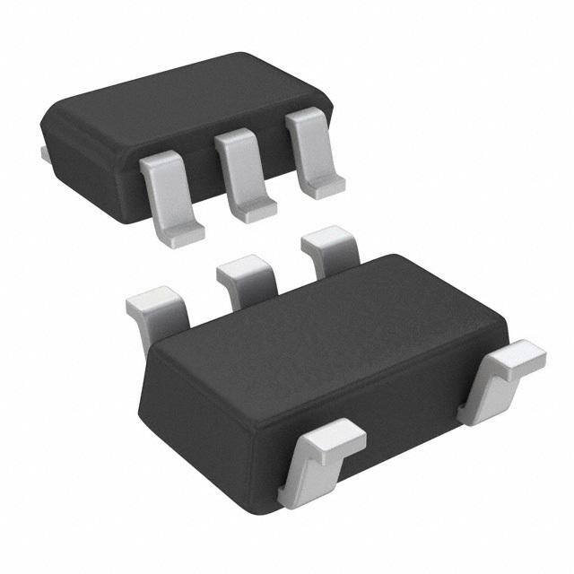
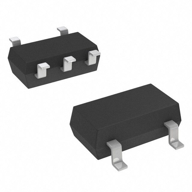
| 描述 | IC REG LDO 5V 0.1A SOT23-5低压差稳压器 5.0V 100mA Positive |
| 产品分类 | |
| 品牌 | STMicroelectronics |
| 产品手册 | |
| 产品图片 |
|
| rohs | 符合RoHS无铅 / 符合限制有害物质指令(RoHS)规范要求 |
| 产品系列 | 电源管理 IC,低压差稳压器,STMicroelectronics LD2981ABM50TR- |
| 数据手册 | |
| 产品型号 | LD2981ABM50TR |
| 产品目录页面 | |
| 产品种类 | 低压差稳压器 |
| 供应商器件封装 | SOT-23-5 |
| 其它名称 | 497-1522-2 |
| 其它有关文件 | http://www.st.com/web/catalog/sense_power/FM142/CL1015/SC312/PF63518?referrer=70071840 |
| 包装 | 带卷 (TR) |
| 商标 | STMicroelectronics |
| 回动电压—最大值 | 3 mV at 0 A |
| 安装类型 | 表面贴装 |
| 安装风格 | SMD/SMT |
| 封装 | Reel |
| 封装/外壳 | SC-74A,SOT-753 |
| 封装/箱体 | SOT-23 |
| 工作温度 | -40°C ~ 125°C |
| 工厂包装数量 | 3000 |
| 最大工作温度 | + 125 C |
| 最大输入电压 | 16 V |
| 最小工作温度 | - 40 C |
| 最小输入电压 | 2.5 V |
| 标准包装 | 3,000 |
| 电压-跌落(典型值) | 0.18V @ 100mA |
| 电压-输入 | 最高 16V |
| 电压-输出 | 5V |
| 电压调节准确度 | 0.75 % |
| 电流-输出 | 100mA |
| 电流-限制(最小值) | - |
| 稳压器拓扑 | 正,固定式 |
| 稳压器数 | 1 |
| 系列 | LD2981ABM |
| 线路调整率 | 0.014 % / V |
| 负载调节 | - 5 mV |
| 输入偏压电流—最大 | 0.08 mA |
| 输出电压 | 5 V |
| 输出电流 | 100 mA |
| 输出端数量 | 1 Output |
| 输出类型 | Fixed |


PDF Datasheet 数据手册内容提取
LD2981 Ultra low-drop voltage regulators with inhibit Datasheet - production data Description The LD2981 is a 100 mA fixed-output voltage regulator. The low-drop voltage and the ultra low quiescent current make them suitable for low noise, low power applications and in battery powered systems. SOT23-5L SOT-89 The quiescent current in sleep mode is less than 1 µA when INHIBIT pin is pulled low. Shutdown logic control function is available on pin n° 3 Features (TTLcompatible). This means that when the device is used as local regulator, it is possible to • Ultra low dropout voltage (0.17 V typ. at 100 put a part of the board in standby, decreasing the mA load, 7 mV typ. at 1 mA load) total power consumption. The LD2981 is • Very low quiescent current (80 µA typ. at no designed to work with low ESR ceramic capacitor. load in on mode; max 1 µA in off mode) Typical applications are in cellular phone, palmtop/laptop computer, personal digital • Guaranteed output current up to 100mA assistant (PDA), personal stereo, camcorder and • Logic-controlled electronic shutdown camera. • Output voltage of 2.5; 3.0; 3.3; 5.0 V • Internal current and thermal limit • ± 0.75% tolerance output voltage available (Aversion) • Output low noise voltage 160 µV RMS • Temperature range: -40 to 125 °C • Small package SOT23-5L and SOT-89 • Fast dynamic response to line and load changes March 2015 DocID6279 Rev 16 1/25 This is information on a product in full production. www.st.com
Contents LD2981 Contents 1 Diagram . . . . . . . . . . . . . . . . . . . . . . . . . . . . . . . . . . . . . . . . . . . . . . . . . . . 3 2 Pin configuration . . . . . . . . . . . . . . . . . . . . . . . . . . . . . . . . . . . . . . . . . . . 4 3 Maximum ratings . . . . . . . . . . . . . . . . . . . . . . . . . . . . . . . . . . . . . . . . . . . . 5 4 Typical application . . . . . . . . . . . . . . . . . . . . . . . . . . . . . . . . . . . . . . . . . . 6 5 Electrical characteristics . . . . . . . . . . . . . . . . . . . . . . . . . . . . . . . . . . . . . 7 6 Typical performance characteristics . . . . . . . . . . . . . . . . . . . . . . . . . . . 10 7 Application notes . . . . . . . . . . . . . . . . . . . . . . . . . . . . . . . . . . . . . . . . . . 13 7.1 External capacitors . . . . . . . . . . . . . . . . . . . . . . . . . . . . . . . . . . . . . . . . . . 13 7.2 Input capacitor . . . . . . . . . . . . . . . . . . . . . . . . . . . . . . . . . . . . . . . . . . . . . 13 7.3 Output capacitor . . . . . . . . . . . . . . . . . . . . . . . . . . . . . . . . . . . . . . . . . . . . 13 7.4 Important . . . . . . . . . . . . . . . . . . . . . . . . . . . . . . . . . . . . . . . . . . . . . . . . . 13 7.5 Inhibit input operation . . . . . . . . . . . . . . . . . . . . . . . . . . . . . . . . . . . . . . . . 13 7.6 Reverse current . . . . . . . . . . . . . . . . . . . . . . . . . . . . . . . . . . . . . . . . . . . . 14 8 Package information . . . . . . . . . . . . . . . . . . . . . . . . . . . . . . . . . . . . . . . . 15 8.1 SOT23-5L package information . . . . . . . . . . . . . . . . . . . . . . . . . . . . . . . . 15 8.2 SOT23-5L packing information . . . . . . . . . . . . . . . . . . . . . . . . . . . . . . . . . 17 8.3 SOT-89 package information . . . . . . . . . . . . . . . . . . . . . . . . . . . . . . . . . . 18 8.4 SOT-89 packing information . . . . . . . . . . . . . . . . . . . . . . . . . . . . . . . . . . . 21 9 Ordering information . . . . . . . . . . . . . . . . . . . . . . . . . . . . . . . . . . . . . . . 23 10 Revision history . . . . . . . . . . . . . . . . . . . . . . . . . . . . . . . . . . . . . . . . . . . 24 2/25 DocID6279 Rev 16
LD2981 Diagram 1 Diagram Figure 1. Schematic diagram DocID6279 Rev 16 3/25 25
Pin configuration LD2981 2 Pin configuration Figure 2. Pin connections (top view) SOT-89 SOT23-5L Table 1. Pin description Pin n° Pin n° Symbol Name and function SOT23-5L SOT-89 1 3 V Input port IN 2 2 GND Ground pin Control switch ON/OFF. Inhibit is not internally pulled-up; it cannot be 3 INHIBIT left floating. Disable the device when connected to GND or to a positive voltage less than 0.18 V 4 NC Not connected 5 1 V Output port OUT Table 2. Thermal data Symbol Parameter SOT23-5L SOT-89 Unit R Thermal resistance junction-case 81 15 °C/W thJC R Thermal resistance junction-ambient 255 110 °C/W thJA 4/25 DocID6279 Rev 16
LD2981 Maximum ratings 3 Maximum ratings Table 3. Absolute maximum ratings Symbol Parameter Value Unit V DC input voltage -0.3 to 16 V I V INHIBIT input voltage -0.3 to 16 V INH I Output current Internally limited O P Power dissipation Internally limited D T Storage temperature range -55 to 150 °C STG T Operating junction temperature range -40 to 125 °C OP Note: Absolute maximum ratings are those values beyond which damage to the device may occur. Functional operation under these condition is not implied. DocID6279 Rev 16 5/25 25
Typical application LD2981 4 Typical application Figure 3. Application circuit Note: Inhibit pin is not internally pulled-up then it must not be left floating. Disable the device when connected to GND or to a positive voltage less than 0.18 V. 6/25 DocID6279 Rev 16
LD2981 Electrical characteristics 5 Electrical characteristics (T = 25 °C, V = V +1 V, C = 1 µF, C = 2.2 µF, I = 1 mA, V = 2 V, unless J I O(NOM) I O O INH otherwise specified). Table 4. Electrical characteristics for LD2981AB Symbol Parameter Test conditions Min. Typ. Max. Unit V Operating input voltage 2.5 16 V OP I = 1 mA 2.977 3 3.023 O V Output voltage I = 1 to 100 mA 2.970 3.030 V O O I = 1 to 100 mA, T = -40 to 125°C 2.925 3.075 O J I = 1 mA 3.275 3.3 3.325 O V Output voltage I = 1 to 100 mA 3.267 3.333 V O O I = 1 to 100 mA, T = -40 to 125°C 3.217 3.383 O J I = 1 mA 4.962 5 5.038 O V Output voltage I = 1 to 100 mA 4.950 5.050 V O O I = 1 to 100 mA, T = -40 to 125°C 4.875 5.125 O J V + 1 < V < 16 V, I = 1 mA 0.003 0.014 ΔV Line regulation O(NOM) IN O %/V O T = -40 to 125°C 0.032 J I = 0 80 100 O I = 0, T = -40 to 125°C 150 O J I = 1 mA 100 150 O Quiescent current IO = 1 mA, TJ= -40 to 125°C 200 ON MODE I = 25 mA 250 400 O I µA Q I = 25 mA, T = -40 to 125°C 800 O J I = 100 mA 1000 1300 O I = 100 mA, T = -40 to 125°C 2600 O J V < 0.3 V 0.8 INH OFF MODE V < 0.15 V, T = -40 to 125°C 2 INH J I = 0 1 3 O I = 0, T = -40 to 125°C 5 O J I = 1mA 7 10 O I = 1mA, T = -40 to 125°C 15 V Dropout voltage (1) O J mV DROP I = 25mA 70 100 O I = 25mA, T = -40 to 125°C 150 O J I = 100mA 180 250 O I = 100mA, T = -40 to 125°C 375 O J DocID6279 Rev 16 7/25 25
Electrical characteristics LD2981 Table 4. Electrical characteristics for LD2981AB (continued) Symbol Parameter Test conditions Min. Typ. Max. Unit I Short circuit current R = 0 150 mA SC L SVR Supply voltage rejection C = 10µF, f = 1KHz 63 dB O V Inhibit input logic low LOW = Output OFF, T = -40 to 125°C 0.18 V INH J V Inhibit input logic high HIGH = Output ON, T = -40 to 125°C 1.6 V INL J V = 0V, T = -40 to 125°C 0 -1 INH J I Inhibit input current µA INH V = 5V, T = -40 to 125°C 5 15 INH J e Output noise voltage B = 300 Hz to 50 KHz, C = 10µF 160 µV N W O RMS T Thermal shutdown 170 °C SHDN 1. For V < 2.5 V dropout voltage can be calculated according to the minimum input voltage in full temperature range. O (T = 25 °C, V = V +1 V, C = 1 µF, C = 2.2 µF, I = 1 mA, V = 2 V, unless J I O(NOM) I O O INH otherwise specified) Table 5. Electrical characteristics for LD2981C Symbol Parameter Test conditions Min. Typ. Max. Unit V Operating input voltage 2.5 16 V OP I = 1 mA 2.468 2.5 2.531 O V Output voltage I = 1 to 100 mA 2.45 2.55 V O O I = 1 to 100 mA, T = -40 to 125°C 2.412 2.587 O J I = 1 mA 2.962 3 3.037 O V Output voltage I = 1 to 100 mA 2.94 3.06 V O O I = 1 to 100 mA, T = -40 to 125°C 2.895 3.105 O J I = 1 mA 3.258 3.3 3.341 O V Output voltage I = 1 to 100 mA 3.234 3.366 V O O I = 1 to 100 mA, T = -40 to 125°C 3.184 3.415 O J I = 1 mA 4.937 5 5.062 O V Output voltage I = 1 to 100 mA 4.9 5.1 V O O I = 1 to 100 mA, T = -40 to 125°C 4.825 5.175 O J V + 1 < V < 16 V, I = 1 mA 0.003 0.014 ΔV Line regulation O(NOM) IN O %/V O T = -40 to 125°C 0.032 J 8/25 DocID6279 Rev 16
LD2981 Electrical characteristics Table 5. Electrical characteristics for LD2981C (continued) Symbol Parameter Test conditions Min. Typ. Max. Unit I = 0 80 100 O I = 0, T = -40 to 125°C 150 O J I = 1 mA 100 150 O Quiescent current IO = 1 mA, TJ= -40 to 125°C 200 ON MODE I = 25 mA 250 400 O I µA Q I = 25 mA, T = -40 to 125°C 800 O J I = 100 mA 1000 1300 O I = 100 mA, T = -40 to 125°C 2600 O J V < 0.3 V 0.8 INH OFF MODE V < 0.15 V, T = -40 to 125°C 2 INH J I = 0 1 3 O I = 0, T = -40 to 125°C 5 O J I = 1 mA 7 10 O I = 1 mA, T = -40 to 125°C 15 V Dropout voltage (1) O J mV DROP I = 25 mA 70 100 O I = 25 mA, T = -40 to 125°C 150 O J I = 100 mA 180 250 O I = 100 mA, T = -40 to 125°C 375 O J I Short circuit current R = 0 150 mA SC L SVR Supply voltage rejection C = 10µF, f = 1KHz 63 dB O V Inhibit input logic low LOW = Output OFF, T = -40 to 125°C 0.18 V INH J V Inhibit input logic high HIGH = Output ON, T = -40 to 125°C 1.6 V INL J V = 0V, T = -40 to 125°C 0 -1 INH J I Inhibit input current µF INH V = 5V, T = -40 to 125°C 5 15 INH J e Output noise voltage B = 300 Hz to 50 KHz, C = 10µF 160 µV N W O RMS T Thermal shutdown 170 °C SHDN 1. For V < 2.5 V dropout voltage can be calculated according to the minimum input voltage in full temperature range. O DocID6279 Rev 16 9/25 25
Typical performance characteristics LD2981 6 Typical performance characteristics (T = 25 °C, V = V +1 V, C = 1 µF, C = 2.2 µF, V = 2 V, unless otherwise J I O(NOM) I O INH specified). Figure 4. Output voltage vs temperature Figure 5. Dropout voltage vs temperature Figure 6. Line regulation vs temperature Figure 7. Load regulation vs temperature Figure 8. Dropout voltage vs temperature Figure 9. Quiescent current vs temperature 10/25 DocID6279 Rev 16
LD2981 Typical performance characteristics Figure 1 0. Quiescent current vs output Figure 11. Off mode quiescent current vs current temperature Figure 12. Quiescent current vs input voltage Figure 13. Dropout voltage vs output current Figure 14. Inhibit input current vs temperature Figure 15. Inhibit voltage vs temperature DocID6279 Rev 16 11/25 25
Typical performance characteristics LD2981 Figure 16. Supply voltage rejection vs Figure 17. Noise voltage vs frequency frequency Figure 18. Best case: highest output version Figure 19. Worst case: lowest output version Figure 20. Load transient response Figure 21. Line transient response VO = 4.7V, IO = 1 to 100mA, CO = 4.7µF (X7R) VI = [VO(NOM) +1V], VO = 4.7V, IO = 100mA, CO = 4.7µF (X7R) 12/25 DocID6279 Rev 16
LD2981 Application notes 7 Application notes 7.1 External capacitors Like any low-dropout regulator, the LD2981 requires external capacitors for regulator stability. This capacitor must be selected to meet the requirements of minimum capacitance and equivalent series resistance. We suggest to solder input and output capacitors as close as possible to the relative pins. 7.2 Input capacitor An input capacitor whose value is 1 µF is required with the LD2981 (amount of capacitance can be increased without limit). This capacitor must be located a distance of not more than 0.5" from the input pin of the device and returned to a clean analog ground. Any good quality ceramic, tantalum or film capacitors can be used for this capacitor. 7.3 Output capacitor The LD2981 is designed specifically to work with ceramic output capacitors. It may also be possible to use Tantalum capacitors, but these are not as attractive for reasons of size and cost. By the way, the output capacitor must meet both the requirement for minimum amount of capacitance and ESR (equivalent series resistance) value. The Figure18 and Figure19 show the allowable ESR range as a function of the output capacitance. These curves represent the stability region over the full temperature and I range. Due to the different O loop gain, the stability improves for higher output versions and so the suggested minimum output capacitor value, if low ESR ceramic type is used, is 1 µF for output voltages equal or major than 3.8 V, 2.2 µF for output voltages from 2.85 to 3.3 V, and 3.3 µF for the other versions. However, if an output capacitor lower than the suggested one is used, it’s possible to make stable the regulator adding a resistor in series to the capacitor (see Figure18 and Figure19 to choose the right value according to the used version and keeping in account that the ESR of ceramic capacitors has been measured @ 100 kHz). 7.4 Important The output capacitor must maintain its ESR in the stable region over the full operating temperature to assure stability. Also, capacitor tolerance and variation with temperature must be considered to assure the minimum amount of capacitance is provided at all times. This capacitor should be located not more than 0.5" from the output pin of the device and returned to a clean analog ground. 7.5 Inhibit input operation The inhibit pin can be used to turn OFF the regulator when pulled low, so drastically reducing the current consumption down to less than 1 µA. When the inhibit feature is not used, this pin must be tied to V to keep the regulator output ON at all times. To assure I proper operation, the signal source used to drive the inhibit pin must be able to swing above DocID6279 Rev 16 13/25 25
Application notes LD2981 and below the specified thresholds listed in the electrical characteristics section under V IH V . Any slew rate can be used to drive the inhibit. IL 7.6 Reverse current The power transistor used in the LD2981 has not an inherent diode connected between the regulator input and output. If the output is forced above the input, no current will flow from the output to the input across the series pass transistor. When a V voltage is applied on REV the output, the reverse current measured, according to the test circuit in Figure22, flows to the GND across the two feedback resistors. This current typical value is 160 µA. R and R 1 2 resistors are implanted type; typical values are, respectively, 42.6 kΩ and 51.150 kΩ. Figure 22. Reverse current test circuit 14/25 DocID6279 Rev 16
LD2981 Package information 8 Package information In order to meet environmental requirements, ST offers these devices in different grades of ECOPACK® packages, depending on their level of environmental compliance. ECOPACK® specifications, grade definitions and product status are available at: www.st.com. ECOPACK® is an ST trademark. 8.1 SOT23-5L package information Figure 23. SOT23-5L package outline (cid:26)(cid:19)(cid:23)(cid:28)(cid:25)(cid:26)(cid:25)(cid:66)(cid:78) DocID6279 Rev 16 15/25 25
Package information LD2981 Table 6. SOT23-5L mechanical data mm Dim. Min. Typ. Max. A 0.90 1.45 A1 0 0.15 A2 0.90 1.30 b 0.30 0.50 c 2.09 0.20 D 2.95 E 1.60 e 0.95 H 2.80 L 0.30 0.60 q 0 8 Figure 24. SOT23-5L recommended footprint (dimensions in mm) (cid:26)(cid:19)(cid:23)(cid:28)(cid:25)(cid:26)(cid:25)(cid:66)(cid:78) 16/25 DocID6279 Rev 16
LD2981 Package information 8.2 SOT23-5L packing information Figure 25. SOT23-5L tape and reel outline Table 7. SOT23-5L tape and reel mechanical data mm Dim. Min. Typ. Max. A 180 C 12.8 13.0 13.2 D 20.2 N 60 T 14.4 Ao 3.13 3.23 3.33 Bo 3.07 3.17 3.27 Ko 1.27 1.37 1.47 Po 3.9 4.0 4.1 P 3.9 4.0 4.1 DocID6279 Rev 16 17/25 25
Package information LD2981 8.3 SOT-89 package information Figure 26. SOT-89 package outline (cid:26)(cid:19)(cid:28)(cid:27)(cid:20)(cid:25)(cid:25)(cid:66)(cid:53)(cid:40)(cid:57)(cid:66)(cid:40) 18/25 DocID6279 Rev 16
LD2981 Package information Table 8. SOT-89 mechanical data mm Dim. Min. Typ. Max. A 1.40 1.60 B 0.44 0.56 B1 0.36 0.48 C 0.35 0.44 C1 0.35 0.44 D 4.40 4.60 D1 1.62 1.83 D3 0.90 E 2.29 2.60 e 1.42 1.57 e1 2.92 3.07 H 3.94 4.25 H1 2.70 3.10 K 1° 8° L 0.89 1.20 R 0.25 b 90° DocID6279 Rev 16 19/25 25
Package information LD2981 Figure 27. SOT-89 recommended footprint (cid:41)(cid:82)(cid:82)(cid:87)(cid:83)(cid:85)(cid:76)(cid:81)(cid:87) 20/25 DocID6279 Rev 16
LD2981 Package information 8.4 SOT-89 packing information Figure 28. SOT-89 carrier tape outline (cid:26)(cid:20)(cid:20)(cid:20)(cid:26)(cid:25)(cid:21)(cid:66)(cid:40) Table 9. SOT-89 carrier tape mechanical data mm. Dim. Values Tolerance Ao 4.52 ± 0.10 Bo 4.91 ± 0.10 Ko 1.90 ± 0.10 F 5.50 ± 0.10 E 1.75 ± 0.10 W 12 ± 0.30 P2 2 ± 0.10 Po 4 ± 0.10 P1 8 ± 0.10 T 0.30 ± 0.10 D ∅ 1.55 ± 0.05 D1 ∅ 1.60 ± 0.10 DocID6279 Rev 16 21/25 25
Package information LD2981 Figure 29. SOT-89 package orientation in carrier tape (cid:53)(cid:58)(cid:49)(cid:42)(cid:36)(cid:34)(cid:45) (cid:54)(cid:84)(cid:70)(cid:83)(cid:1)(cid:69)(cid:74)(cid:83)(cid:70)(cid:68)(cid:85)(cid:74)(cid:80)(cid:79)(cid:1)(cid:80)(cid:71)(cid:1)(cid:71)(cid:70)(cid:70)(cid:69) (cid:1) (cid:52)(cid:53)(cid:1)(cid:4)(cid:17)(cid:17)(cid:20)(cid:18)(cid:26)(cid:20)(cid:19) 22/25 DocID6279 Rev 16
LD2981 Ordering information 9 Ordering information Table 10. Order code AB Version C Version Output voltage SOT23-5L SOT-89 SOT23-5L SOT-89 LD2981CM25TR 2.5 V LD2981ABM30TR LD2981CM30TR 3.0 V LD2981ABM33TR LD2981ABU33TR LD2981CM33TR LLD2981CU33TR 3.3 V LD2981ABM50TR LD2981ABU50TR LD2981CM33TR LD2981CU50TR 5.0 V DocID6279 Rev 16 23/25 25
Revision history LD2981 10 Revision history Table 11. Document revision history Date Revision Changes 25-Jul-2006 12 Order codes updated. 14-Feb-2008 13 Added: Table1 on page1. 14-Jul-2008 14 Modified: Table1 on page1 and Table10 on page23. Document name changed from LD2981ABxx and LD2981Cxx to LD2981. Updated Table4 and Table5. 25-Nov-2013 15 Updated Section8: Package information and Section8.4: SOT-89 packing information. Minor text changes in title, in features and description in cover page. Updated Section8: Package information. 16-Mar-2015 16 Minor text changes. 24/25 DocID6279 Rev 16
LD2981 IMPORTANT NOTICE – PLEASE READ CAREFULLY STMicroelectronics NV and its subsidiaries (“ST”) reserve the right to make changes, corrections, enhancements, modifications, and improvements to ST products and/or to this document at any time without notice. Purchasers should obtain the latest relevant information on ST products before placing orders. ST products are sold pursuant to ST’s terms and conditions of sale in place at the time of order acknowledgement. Purchasers are solely responsible for the choice, selection, and use of ST products and ST assumes no liability for application assistance or the design of Purchasers’ products. No license, express or implied, to any intellectual property right is granted by ST herein. Resale of ST products with provisions different from the information set forth herein shall void any warranty granted by ST for such product. ST and the ST logo are trademarks of ST. All other product or service names are the property of their respective owners. Information in this document supersedes and replaces information previously supplied in any prior versions of this document. © 2015 STMicroelectronics – All rights reserved DocID6279 Rev 16 25/25 25