ICGOO在线商城 > 集成电路(IC) > PMIC - 稳压器 - 线性 > LP3875ES-2.5/NOPB

 Datasheet下载
- 型号: LP3875ES-2.5/NOPB
- 制造商: Texas Instruments
- 库位|库存: xxxx|xxxx
- 要求:
| 数量阶梯 | 香港交货 | 国内含税 |
| +xxxx | $xxxx | ¥xxxx |
查看当月历史价格
查看今年历史价格
LP3875ES-2.5/NOPB产品简介:
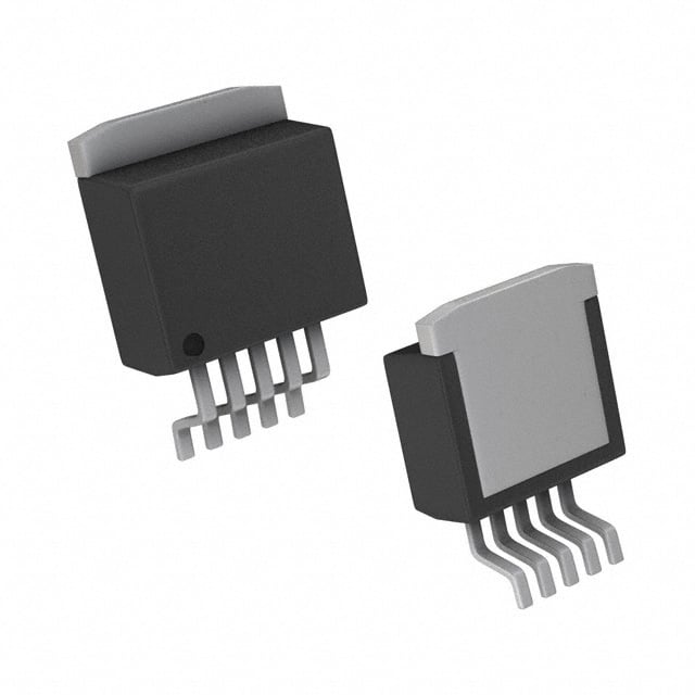
ICGOO电子元器件商城为您提供LP3875ES-2.5/NOPB由Texas Instruments设计生产,在icgoo商城现货销售,并且可以通过原厂、代理商等渠道进行代购。 LP3875ES-2.5/NOPB价格参考¥9.63-¥27.48。Texas InstrumentsLP3875ES-2.5/NOPB封装/规格:PMIC - 稳压器 - 线性, Linear Voltage Regulator IC Positive Fixed 1 Output 2.5V 1.5A DDPAK/TO-263-5。您可以下载LP3875ES-2.5/NOPB参考资料、Datasheet数据手册功能说明书,资料中有LP3875ES-2.5/NOPB 详细功能的应用电路图电压和使用方法及教程。
Texas Instruments 的 LP3875ES-2.5/NOPB 是一款线性稳压器(LDO),输出电压为固定的2.5V,具有低噪声、高纹波抑制比(PSRR)和快速瞬态响应等特点。该器件广泛应用于对电源噪声敏感、要求稳定供电的电子系统中。

典型应用场景包括:

1. 便携式电子产品:如智能手机、平板电脑、数码相机等,用于为处理器、传感器或射频模块提供稳定电源。
2. 通信设备:用于无线基站、路由器或接入点中,为射频前端、时钟电路或数据转换器供电。
3. 工业控制系统:如PLC、工业仪表和传感器模块,提供低噪声电源以确保信号精度。
4. 音频设备:如便携式音频播放器或高保真音响系统,用于为模拟电路或放大器供电,降低电源噪声对音质的影响。
5. 测试与测量仪器:如示波器、万用表等,为内部精密模拟和数字电路提供干净电源。

该器件采用热增强型封装(如ES封装),有助于在较高负载下保持稳定工作温度,适合空间受限但需要良好散热性能的设计。此外,其低压差特性使其在电池供电系统中特别有用,可延长电池使用寿命。
| 参数 | 数值 |
| 产品目录 | 集成电路 (IC)半导体 |
| 描述 | IC REG LDO 2.5V 1.5A DDPAK低压差稳压器 1.5A Low Dropout LDO |
| 产品分类 | |
| 品牌 | Texas Instruments |
| 产品手册 | |
| 产品图片 |
|
| rohs | 符合RoHS含铅 / 不受限制有害物质指令(RoHS)规范要求限制 |
| 产品系列 | 电源管理 IC,低压差稳压器,Texas Instruments LP3875ES-2.5/NOPB- |
| 数据手册 | |
| 产品型号 | LP3875ES-2.5/NOPB |
| PSRR/纹波抑制—典型值 | 73 dB |
| 产品 | Fast Ultra Low Dropout Linear Regulator |
| 产品目录页面 | |
| 产品种类 | 低压差稳压器 |
| 供应商器件封装 | DDPAK/TO-263-5 |
| 其它名称 | *LP3875ES-2.5/NOPB |
| 包装 | 管件 |
| 商标 | Texas Instruments |
| 回动电压—最大值 | 550 mV |
| 安装类型 | 表面贴装 |
| 安装风格 | SMD/SMT |
| 封装/外壳 | TO-263-6,D²Pak(5 引线+接片),TO-263BA |
| 封装/箱体 | TO-263-5 |
| 工作温度 | -40°C ~ 125°C |
| 工厂包装数量 | 45 |
| 最大工作温度 | + 125 C |
| 最大输入电压 | 7 V |
| 最小工作温度 | - 40 C |
| 最小输入电压 | 2.5 V |
| 标准包装 | 45 |
| 电压-跌落(典型值) | 0.38V @ 1.5A |
| 电压-输入 | 最高 7V |
| 电压-输出 | 2.5V |
| 电流-输出 | 1.5A |
| 电流-限制(最小值) | - |
| 稳压器拓扑 | 正,固定式 |
| 稳压器数 | 1 |
| 类型 | Ultra Low Dropout Voltage |
| 系列 | LP3875 |
| 线路调整率 | 0.06 % |
| 设计资源 | http://www.digikey.com/product-highlights/cn/zh/texas-instruments-webench-design-center/3176 |
| 负载调节 | 0.12 % |
| 输出电压 | 2.5 V |
| 输出电压容差 | +/- 3 % |
| 输出电流 | 1.5 A |
| 输出端数量 | 1 Output |
| 输出类型 | Fixed |


- 商务部:美国ITC正式对集成电路等产品启动337调查
- 曝三星4nm工艺存在良率问题 高通将骁龙8 Gen1或转产台积电
- 太阳诱电将投资9.5亿元在常州建新厂生产MLCC 预计2023年完工
- 英特尔发布欧洲新工厂建设计划 深化IDM 2.0 战略
- 台积电先进制程称霸业界 有大客户加持明年业绩稳了
- 达到5530亿美元!SIA预计今年全球半导体销售额将创下新高
- 英特尔拟将自动驾驶子公司Mobileye上市 估值或超500亿美元
- 三星加码芯片和SET,合并消费电子和移动部门,撤换高东真等 CEO
- 三星电子宣布重大人事变动 还合并消费电子和移动部门
- 海关总署:前11个月进口集成电路产品价值2.52万亿元 增长14.8%


PDF Datasheet 数据手册内容提取
Product Sample & Technical Tools & Support & Folder Buy Documents Software Community LP3872,LP3875 SNVS227H–FEBRUARY2003–REVISEDJANUARY2015 LP387x 1.5-A Fast Ultra-Low-Dropout Linear Regulators 1 Features 3 Description • InputVoltageRange:2.5Vto7V The LP387x series of fast ultra low-dropout linear 1 regulators operate from a 2.5-V to 7-V input supply. • UltraLow-DropoutVoltage Wide range of preset output voltage options are • LowGroundPinCurrent available. These ultra low-dropout linear regulators • LoadRegulationof0.06% respond very quickly to step changes in load, which makes them suitable for low-voltage microprocessor • 10-nAQuiescentCurrentinShutdownMode applications. The LP3872 and LP3875 are developed • EnsuredOutputCurrentof1.5-ADC on a CMOS process which allows low quiescent • AvailableinDDPAK/TO-263,TO-220,and current operation independent of output load current. SOT-223Packages This CMOS process also allows the LP3872 and LP3875 to operate under extremely low dropout • OutputVoltageAccuracy ± 1.5% conditions. • ERROR FlagforOutputStatus Dropout Voltage: Ultra low-dropout voltage; typically • SenseOptionImprovesLoadRegulation 38 mV at 150-mA load current and 380 mV at 1.5-A • MinimumOutputCapacitorRequirements loadcurrent. • Overtemperature/OvercurrentProtection Ground Pin Current: Typically 6 mA at 1.5-A load • −40°Cto125°CJunctionTemperatureRange current. Shutdown Mode: Typically 10-nA quiescent current 2 Applications whenthe SDpinispulledlow. • MicroprocessorPowerSupplies ERROR Flag: ERROR flag goes low when the output • GTL,GTL+,BTL,andSSTLBusTerminators voltage drops 10% below nominal value (LP3872 • PowerSuppliesforDSPs only). • SCSITerminators SENSE: Sense pin improves regulation at remote • PostRegulators loads(LP3875only). • HighEfficiencyLinearRegulators Precision Output Voltage: Multiple output voltage • BatteryChargers options are available ranging from 1.8 V to 5 V with a specified accuracy of ±1.5% at room temperature, • OtherBattery-PoweredApplications and ±3.0% over all conditions (varying line, load, and space temperature). space space DeviceInformation(1) space PARTNUMBER PACKAGE BODYSIZE(NOM) space SOT-223(5) 6.50mm×3.56mm LP3872 TO-263(5) 10.16mm×8.42mm LP3872TypicalApplicationCircuit SOT-223(5) 6.50mm×3.56mm LP3875 TO-263(5) 10.16mm×8.42mm TO-220(5) 14.986mm×10.16mm (1) For all available packages, see the orderable addendum at theendofthedatasheet. LP3875TypicalApplicationCircuit *SDandERRORpinsmustbepulledhigh througha10-kΩpullupresistor.Connect theERRORpintogroundifthisfunctionis notused.SeetheShutdownModeand ERRORFlagOperationsections. *SDmustbepulledhighthrougha10-kΩ pullupresistor.SeetheShutdownMode section. 1 An IMPORTANT NOTICE at the end of this data sheet addresses availability, warranty, changes, use in safety-critical applications, intellectualpropertymattersandotherimportantdisclaimers.PRODUCTIONDATA.
LP3872,LP3875 SNVS227H–FEBRUARY2003–REVISEDJANUARY2015 www.ti.com Table of Contents 1 Features.................................................................. 1 7.3 FeatureDescription...................................................8 2 Applications........................................................... 1 7.4 DeviceFunctionalModes..........................................9 3 Description............................................................. 1 8 ApplicationandImplementation........................ 11 4 RevisionHistory..................................................... 2 8.1 ApplicationInformation............................................11 8.2 TypicalApplication..................................................11 5 PinConfigurationandFunctions......................... 3 9 PowerSupplyRecommendations...................... 16 6 Specifications......................................................... 4 10 Layout................................................................... 16 6.1 AbsoluteMaximumRatings......................................4 6.2 ESDRatings ............................................................4 10.1 LayoutGuidelines.................................................16 6.3 RecommendedOperatingConditions.......................4 10.2 LayoutExamples...................................................17 6.4 ThermalInformation..................................................4 11 DeviceandDocumentationSupport................. 18 6.5 ElectricalCharacteristics...........................................5 11.1 RelatedLinks........................................................18 6.6 TypicalCharacteristics..............................................6 11.2 Trademarks...........................................................18 7 DetailedDescription.............................................. 8 11.3 ElectrostaticDischargeCaution............................18 7.1 Overview...................................................................8 11.4 Glossary................................................................18 7.2 FunctionalBlockDiagram.........................................8 12 Mechanical,Packaging,andOrderable Information........................................................... 18 4 Revision History NOTE:Pagenumbersforpreviousrevisionsmaydifferfrompagenumbersinthecurrentversion. ChangesfromRevisionG(December2014)toRevisionH Page • AddedInputvoltagerangeasfirstFeature ........................................................................................................................... 1 • Added"(LP3872only)" .......................................................................................................................................................... 1 • Added"(LP3875only)" .......................................................................................................................................................... 1 • ChangedallVINandVOUTpinnamestoINandOUTindrawingsandtext........................................................................ 1 • Changedfootnotestoappearundereachtable .................................................................................................................... 4 • DeletedCDMfootnote ........................................................................................................................................................... 4 • DeletedlastsentenceofShort-CircuitProtectionsubsection ............................................................................................... 9 ChangesfromRevisionF(April2013)toRevisionG Page • AddedPinConfigurationandFunctionssection,ESDRatingstable,FeatureDescriptionsection,DeviceFunctional Modes,ApplicationandImplementationsection,PowerSupplyRecommendationssection,Layoutsection,Device andDocumentationSupportsection,andMechanical,Packaging,andOrderableInformationsection;update thermalvalues ....................................................................................................................................................................... 1 2 SubmitDocumentationFeedback Copyright©2003–2015,TexasInstrumentsIncorporated ProductFolderLinks:LP3872 LP3875
LP3872,LP3875 www.ti.com SNVS227H–FEBRUARY2003–REVISEDJANUARY2015 5 Pin Configuration and Functions 5-PinTO-220 5-PinDDPAK/TO-263 NDHPackage KTTPackage TopView TopView 5-PinSOT-223 NDCPackage TopView GND 5 1 2 3 4 SD IN OUT ERROR /SENSE PinFunctions PIN NUMBER LP3872 LP3875 I/O DESCRIPTION NAME TO-220 TO-220 SOT-223 SOT-223 DDPAK/TO-263 DDPAK/TO-263 SD 1 1 1 1 I Shutdown IN 2 2 2 2 I Inputsupply OUT 4 3 4 3 O Outputvoltage ERROR 5 4 — — O Errorflag SENSE — — 5 4 I Remotevoltagesense GND 3 5 3 5 — Ground Copyright©2003–2015,TexasInstrumentsIncorporated SubmitDocumentationFeedback 3 ProductFolderLinks:LP3872 LP3875
LP3872,LP3875 SNVS227H–FEBRUARY2003–REVISEDJANUARY2015 www.ti.com 6 Specifications 6.1 Absolute Maximum Ratings(1)(2) IfMilitary/Aerospacespecifieddevicesarerequired,contacttheTexasInstrumentsSalesOffice/Distributorsforavailability andspecifications. MIN MAX UNIT Leadtemperature(soldering,5sec.) 260 °C Powerdissipation(3) Internallylimited INpintoGNDpinvoltage −0.3 7.5 V Shutdown(SD)pintoGNDpinvoltage −0.3 7.5 V OUTpintoGNDpinvoltage(4), (5) −0.3 6 V I Short-circuitprotected OUT ERRORpintoGNDpinvoltage V V IN SENSEpintoGNDpinvoltage V V OUT Storagetemperature,T −65 150 °C stg (1) StressesbeyondthoselistedunderAbsoluteMaximumRatings(1)(2)maycausepermanentdamagetothedevice.Thesearestress ratingsonly,whichdonotimplyfunctionaloperationofthedeviceattheseoranyotherconditionsbeyondthoseindicatedunder RecommendedOperatingConditions.Exposuretoabsolute-maximum-ratedconditionsforextendedperiodsmayaffectdevicereliability. (2) IfMilitary/Aerospacespecifieddevicesarerequired,pleasecontacttheTISalesOffice/Distributorsforavailabilityandspecifications. (3) Internalthermalshutdowncircuitryprotectsthedevicefrompermanentdamage. (4) Ifusedinadual-supplysystemwheretheregulatorloadisreturnedtoanegativesupply,theoutputmustbediode-clampedtoground. (5) TheoutputPMOSstructurecontainsadiodebetweentheINandOUTpins.Thisdiodeisnormallyreversebiased.Thisdiodewillget forwardbiasedifthevoltageattheoutputterminalisforcedtobehigherthanthevoltageattheinputterminal.Thisdiodecantypically withstand200mAofDCcurrentand1Aofpeakcurrent. 6.2 ESD Ratings VALUE UNIT V Electrostaticdischarge Humanbodymodel(HBM),perANSI/ESDA/JEDECJS-001(1) ±2000 V (ESD) (1) JEDECdocumentJEP155statesthat500-VHBMallowssafemanufacturingwithastandardESDcontrolprocess. 6.3 Recommended Operating Conditions MIN MAX UNIT V supplyvoltage (1) 2.5 7 V IN Shutdown(SD)voltage −0.3 7 V Maximumoperatingcurrent(DC)I 1.5 A OUT Junctiontemperature –40 125 °C (1) TheminimumoperatingvalueforV isequaltoeither[V +V ]or2.5V,whicheverisgreater. IN OUT(NOM) DROPOUT 6.4 Thermal Information LP3872,LP3875 LP3875 THERMALMETRIC(1) NDC(SOT-223) KTT(TO-263) NDH(TO-220) UNIT 5PINS 5PINS 5PINS R Junction-to-ambientthermalresistance 65.2 40.3 32 θJA R Junction-to-case(top)thermalresistance 47.2 43.4 43.8 θJC(top) R Junction-to-boardthermalresistance 9.9 23.1 18.6 θJB °C/W ψ Junction-to-topcharacterizationparameter 3.4 11.5 8.8 JT ψ Junction-to-boardcharacterizationparameter 9.7 22 18 JB R Junction-to-case(bottom)thermalresistance n/a 1 1.2 θJC(bot) (1) Formoreinformationabouttraditionalandnewthermalmetrics,seetheICPackageThermalMetricsapplicationreport,SPRA953. 4 SubmitDocumentationFeedback Copyright©2003–2015,TexasInstrumentsIncorporated ProductFolderLinks:LP3872 LP3875
LP3872,LP3875 www.ti.com SNVS227H–FEBRUARY2003–REVISEDJANUARY2015 6.5 Electrical Characteristics Unlessotherwisespecified:T =25°C,V =V +1V,I =10mA,C =10µF,V =2V. J IN O(NOM) L OUT SD PARAMETER TESTCONDITIONS MIN(1) TYP(2) MAX(1) UNIT Outputvoltagetolerance (3) V +1V≤V ≤7V,10mA≤I ≤1.5A –1.5% 0% 1.5% OUT IN L VOUT VOUT+1V≤VIN≤7V,10mA≤IL≤1.5A, –3% 3% –40°C≤T ≤125°C J Outputvoltagelineregulation (3) V +1V≤V ≤7V 0.02% OUT IN ΔV OL V +1V≤V ≤7V,–40°C≤T ≤125°C 0.06% OUT IN J ΔVO/ Outputvoltageloadregulation (3) 10mA≤IL≤1.5A 0.06% ΔIOUT 10mA≤IL≤1.5A,–40°C≤TJ≤125°C 0.12% I =150mA 38 50 L VIN- Dropoutvoltage (4) IL=150mA,–40°C≤TJ≤125°C 60 mV VOUT IL=1.5A 380 450 I =1.5A,–40°C≤T ≤125°C 550 L J I =150mA 5 9 L Groundpincurrentinnormal IL=150mA,–40°C≤TJ≤125°C 10 I mA GND operationmode I =1.5A 6 14 L I =1.5A,–40°C≤T ≤125°C 15 L J Groundpincurrentinshutdown V ≤0.3V 0.01 10 µA SD IGND mode –40°C≤T ≤85°C 50 J I Peakoutputcurrent V ≥V –4% 1.8 A O(PK) OUT O(NOM) SHORTCIRCUITPROTECTION I Short-circuitcurrent 3.2 A SC SHUTDOWNINPUT Output=High V IN Output=High,–40°C≤T ≤125°C 2 J V Shutdownthreshold V SDT Output=Low 0 Output=Low,–40°C≤T ≤125°C 0.3 J T Turnoffdelay I =1.5A 20 µs dOFF L T Turnondelay I =1.5A 25 µs dON L I SDinputcurrent V =V 1 nA SD SD IN ERRORFLAG Threshold See(5) 10% V T See(5),–40°C≤T ≤125°C 5% 16% J Thresholdhysteresis See(5) 5% V TH See(5),–40°C≤T ≤125°C 2% 8% J ERRORflagsaturation I =100µA 0.02 sink V V EF(Sat) I =100µA,–40°C≤T ≤125°C 0.1 sink J Td Flagresetdelay 1 µs I ERRORflagpinleakagecurrent 1 nA lk I ERRORflagpinsinkcurrent V =0.5V 1 mA max Error (1) Limitsarespecifiedbytesting,design,orstatisticalcorrelation. (2) Typicalnumbersareat25°Candrepresentthemostlikelyparametricnorm. (3) Outputvoltagelineregulationisdefinedasthechangeinoutputvoltagefromthenominalvalueduetochangeintheinputlinevoltage. Outputvoltageloadregulationisdefinedasthechangeinoutputvoltagefromthenominalvalueduetochangeinloadcurrent.Theline andloadregulationspecificationcontainsonlythetypicalnumber.However,thelimitsforlineandloadregulationareincludedinthe outputvoltagetolerancespecification. (4) Dropoutvoltageisdefinedastheminimuminputtooutputdifferentialvoltageatwhichtheoutputdrops2%belowthenominalvalue. Dropoutvoltagespecificationappliesonlytooutputvoltagesof2.5Vandabove.Foroutputvoltagesbelow2.5V,thedropoutvoltageis nothingbuttheinputtooutputdifferential,becausetheminimuminputvoltageis2.5V. (5) ERRORFlagthresholdandhysteresisarespecifiedaspercentageofregulatedoutputvoltage.SeeERRORFlagOperation. Copyright©2003–2015,TexasInstrumentsIncorporated SubmitDocumentationFeedback 5 ProductFolderLinks:LP3872 LP3875
LP3872,LP3875 SNVS227H–FEBRUARY2003–REVISEDJANUARY2015 www.ti.com Electrical Characteristics (continued) Unlessotherwisespecified:T =25°C,V =V +1V,I =10mA,C =10µF,V =2V. J IN O(NOM) L OUT SD PARAMETER TESTCONDITIONS MIN(1) TYP(2) MAX(1) UNIT ACPARAMETERS V =V +1V,C =10µF IN OUT OUT 73 V =3.3V,f=120Hz OUT PSRR Ripplerejection dB V =V +0.5V,C =10µF IN OUT OUT 57 V =3.3V,f=120Hz OUT ρ Outputnoisedensity f=120Hz 0.8 µV n(l/f) BW=10Hz–100kHz,VOUT=2.5V 150 µV e Outputnoisevoltage n BW=300Hz–300kH,V =2.5V 100 (rms) OUT 6.6 Typical Characteristics Unlessotherwisespecified:T =25°C,C =10µF,C =10µF,SDpinistiedtoV ,V =2.5V,V =V +1V,I = J OUT IN IN OUT IN O(NOM) L 10mA 600 6 V) 500 mA) 5 LTAGE (m 400 125o C 25o C URRENT( 4 O C OUT V 300 D PIN 3 ROP 200 -40oC OUN 2 D R 100 G 1 0 0 0 0.5 1 1.5 1.8 2.3 2.8 3.3 3.8 4.3 5.0 OUTPUT LOAD CURRENT (A) OUTPUTVOLTAGE (V) Figure1.DropoutVoltagevsOutputLoadCurrent Figure2.GroundCurrentvsOutputVoltage I =1.5A L 10 14 1 V)OUT 12 A)P % of 10 WN I (Q 0.1 HOLD ( 8 O S 6 D E T R U H H T 4 S 0.01 R O R 2 R E 0.001 0 -40 -20 0 20 40 60 80 100 125 -40 -20 0 20 40 60 80 100 125 TEMPERATURE (oC) JUNCTION TEMPERATURE (oC) Figure3.ShutdownI vsJunctionTemperature Figure4.ErrorflagThresholdvsJunctionTemperature Q 6 SubmitDocumentationFeedback Copyright©2003–2015,TexasInstrumentsIncorporated ProductFolderLinks:LP3872 LP3875
LP3872,LP3875 www.ti.com SNVS227H–FEBRUARY2003–REVISEDJANUARY2015 Typical Characteristics (continued) Unlessotherwisespecified:T =25°C,C =10µF,C =10µF,SDpinistiedtoV ,V =2.5V,V =V +1V,I = J OUT IN IN OUT IN O(NOM) L 10mA 3 3 2.5 mV) 2.5 AD REGULATION (mV/A) 1.512 OLT CHANGE in V (IN 1.512 O V DC L 0.5 V/OUT 0.5 ' 0 0 -40 -20 0 20 40 60 80 100 125 -40 -20 0 20 40 60 80 100 125 JUNCTION TEMPERATURE (oC) JUNCTION TEMPERATURE (oC) Figure5.DCLoadReg.vsJunctionTemperature Figure6.DCLineRegulationvsTemperature 3.000 2.500 IL = 100mA CIN = COUT = 10PF (Hz 2.000 V/ E (P 1.500 S NOI 1.000 0.500 0.000 100 1k 10k 100k FREQUENCY (Hz) Figure7.NoisevsFrequency Copyright©2003–2015,TexasInstrumentsIncorporated SubmitDocumentationFeedback 7 ProductFolderLinks:LP3872 LP3875
LP3872,LP3875 SNVS227H–FEBRUARY2003–REVISEDJANUARY2015 www.ti.com 7 Detailed Description 7.1 Overview The LP387x linear regulators are designed to provide an ultra-low-dropout voltage with excellent transient response and load/line regulation. For battery-powered always-on type applications, the very low quiescent current of LP387x in shutdown mode helps reduce battery drain. For applications where load is not placed close to the regulator, LP3875 incorporates a voltage sense circuit to improve voltage regulation at the point of load. ERROR outputpinofLP3872canbeusedinthesystemtoflagalow-voltagecondition. 7.2 Functional Block Diagram Figure8. LP3872 Figure9. LP3875 7.3 Feature Description 7.3.1 Shutdown(SD) The LM387x devices have a shutdown feature that turns the device off and reduces the quiescent current to 10 nA,typical. 8 SubmitDocumentationFeedback Copyright©2003–2015,TexasInstrumentsIncorporated ProductFolderLinks:LP3872 LP3875
LP3872,LP3875 www.ti.com SNVS227H–FEBRUARY2003–REVISEDJANUARY2015 Feature Description (continued) 7.3.2 LoadVoltageSense In applications where the regulator output is not very close to the load, LP3875 can provide better remote load regulation using the SENSE pin. Figure 10 depicts the advantage of the SENSE option. LP3872 regulates the voltage at the OUT pin. Hence, the voltage at the remote load will be the regulator output voltage minus the drop across the trace resistance. For example, in the case of a 3.3-V output, if the trace resistance is 100 mΩ, the voltage at the remote load will be 3.15 V with 1.5 A of load current, I . The LP3875 regulates the voltage at LOAD the sense pin. Connecting the sense pin to the remote load will provide regulation at the remote load, as shown inFigure10.Ifthesenseoptionpinisnotrequired,theSENSEpinmustbeconnectedtotheOUTpin. Figure10. ImprovingRemoteLoadRegulationUsingLP3875 7.3.3 Short-CircuitProtection The LP3872 and LP3875 devices are short-circuit protected and in the event of a peak overcurrent condition, the short-circuitcontrolloopwillrapidlydrivetheoutputPMOSpasselementoff.Oncethepowerpasselementshuts down, the control loop will rapidly cycle the output on and off until the average power dissipation causes the thermalshutdowncircuittorespondtoservotheon/offcyclingtoalowerfrequency. 7.3.4 LowDropoutVoltage The LP387x devices feature an ultra-low-dropout voltage, typically 38 mV at 150-mA load current and 380 mV at 1.5-Aloadcurrent. 7.4 Device Functional Modes 7.4.1 ShutdownMode A CMOS Logic low level signal at the shutdown (SD) pin will turn off the regulator. The SD pin must be actively terminated through a 10-kΩ pullup resistor for a proper operation. If this pin is driven from a source that actively pulls high and low (such as a CMOS rail to rail comparator), the pullup resistor is not required. This pin must be tiedtoV ifnotused. IN 7.4.2 ActiveMode Whenvoltageat SDpinoftheLP387xdeviceisatlogichighlevel,thedeviceisinnormalmodeofoperation. 7.4.3 ERROR FlagOperation The LP3872 and LP3875 produces a logic low signal at the ERROR Flag pin when the output drops out of regulation due to low input voltage, current limiting, or thermal limiting. This flag has a built-in hysteresis. The timing diagram in Figure 11 shows the relationship between the ERROR flag and the output voltage. In this example,theinputvoltageischangedtodemonstratethefunctionalityofthe ERROR Flag. Copyright©2003–2015,TexasInstrumentsIncorporated SubmitDocumentationFeedback 9 ProductFolderLinks:LP3872 LP3875
LP3872,LP3875 SNVS227H–FEBRUARY2003–REVISEDJANUARY2015 www.ti.com Device Functional Modes (continued) The internal ERROR flag comparator has an open-drain output stage. Hence, the ERROR pin should be pulled highthroughapullupresistor.AlthoughtheERROR flagpincansinkcurrentof1mA,thiscurrentisenergydrain from the input supply. Hence, the value of the pullup resistor should be in the range of 10 kΩ to 1 MΩ. The ERROR pin must be connected to ground if this function is not used. It should also be noted that when the SD pinispulledlow,theERROR pinisforcedtobeinvalidforreasonsofsavingpowerinshutdownmode. Figure11. ERROR FlagOperation 10 SubmitDocumentationFeedback Copyright©2003–2015,TexasInstrumentsIncorporated ProductFolderLinks:LP3872 LP3875
LP3872,LP3875 www.ti.com SNVS227H–FEBRUARY2003–REVISEDJANUARY2015 8 Application and Implementation NOTE Information in the following applications sections is not part of the TI component specification, and TI does not warrant its accuracy or completeness. TI’s customers are responsible for determining suitability of components for their purposes. Customers should validateandtesttheirdesignimplementationtoconfirmsystemfunctionality. 8.1 Application Information The LP387x devices are linear regulators designed to provide high load current of up to 1.5 A, low dropout voltage, and low quiescent current in shutdown mode. Figure 12 and Figure 13 show the typical application circuitforthesedevices. 8.1.1 DropoutVoltage The dropout voltage of a regulator is defined as the minimum input-to-output differential required to stay within 2% of the nominal output voltage. For CMOS LDOs, the dropout voltage is the product of the load current and theR oftheinternalMOSFET. ds(on) 8.1.2 ReverseCurrentPath The internal MOSFET in LP3872 and LP3875 has an inherent parasitic diode. During normal operation, the input voltage is higher than the output voltage and the parasitic diode is reverse biased. However, if the output is pulledabovetheinputinanapplication,thencurrentflowsfromtheoutputtotheinputastheparasiticdiodegets forwardbiased.Theoutputcanbepulledabovetheinputaslongasthecurrentintheparasiticdiodeislimitedto 200-mAcontinuousand1-Apeak. 8.2 Typical Application *SDandERRORpinsmustbepulledhighthrougha10-kΩpullupresistor.ConnecttheERRORpintogroundifthis functionisnotused.SeetheShutdownModeandERRORFlagOperationsections. Figure12. LP3872TypicalApplicationCircuit *SDmustbepulledhighthrougha10-kΩpullupresistor.SeetheShutdownModesection. Figure13. LP3875TypicalApplicationCircuit Copyright©2003–2015,TexasInstrumentsIncorporated SubmitDocumentationFeedback 11 ProductFolderLinks:LP3872 LP3875
LP3872,LP3875 SNVS227H–FEBRUARY2003–REVISEDJANUARY2015 www.ti.com Typical Application (continued) 8.2.1 DesignRequirements Table1.DesignParameters DESIGNPARAMETER EXAMPLEVALUE Inputvoltagerange 2.5Vto7V Outputvoltage 1.8V Outputcurrent 1.5A Outputcapacitor 10µF Inputcapacitor 10µF OutputcapacitorESRrange 100mΩto4Ω 8.2.2 DetailedDesignProcedure 8.2.2.1 PowerDissipationandDeviceOperation The permissible power dissipation for any package is a measure of the capability of the device to pass heat from the power source, the junctions of the IC, to the ultimate heat sink, the ambient environment. Thus, the power dissipation depends on the ambient temperature and the thermal resistance across the various interfaces betweenthediejunctionandambientair. ThemaximumallowablepowerdissipationforthedeviceinagivenpackagecanbecalculatedusingEquation1: P =((T –T )/R ) (1) D-MAX J-MAX A θJA TheactualpowerbeingdissipatedinthedevicecanberepresentedbyEquation2: P =(V –V )×I (2) D IN OUT OUT Equation 1 and Equation 2 establish the relationship between the maximum power dissipation allowed due to thermal consideration, the voltage drop across the device, and the continuous current capability of the device. These two equations should be used to determine the optimum operating conditions for the device in the application. In applications where lower power dissipation (P ) and/or excellent package thermal resistance (R ) is present, D θJA themaximumambienttemperature(T )maybeincreased. A-MAX In applications where high power dissipation and/or poor package thermal resistance is present, the maximum ambient temperature (T ) may have to be derated. T is dependent on the maximum operating junction A-MAX A-MAX temperature (T = 125°C), the maximum allowable power dissipation in the device package in the J-MAX-OP application (P ), and the junction-to ambient thermal resistance of the part/package in the application (R ), D-MAX θJA asgivenbyEquation3: T =(T –(R ×P )) (3) A-MAX J-MAX-OP θJA D-MAX Alternately, if T can not be derated, the P value must be reduced. This can be accomplished by reducing A-MAX D V in the V – V term as long as the minimum V is met, or by reducing the I term, or by some IN IN OUT IN OUT combinationofthetwo. 8.2.2.2 ExternalCapacitors Like any low-dropout regulator, external capacitors are required to assure stability. These capacitors must be correctlyselectedforproperperformance. • Input Capacitor: An input capacitor of at least 10 µF is required. Ceramic, tantalum, or Electrolytic capacitors maybeused,andcapacitancemaybeincreasedwithoutlimit. • Output Capacitor: An output capacitor is required for loop stability. It must be located less than 1 cm from the device and connected directly to the output and ground pins using traces which have no other currents flowingthroughthem(seeLayout section). The minimum value of output capacitance that can be used for stable full-load operation is 10 µF, but it may be increased without limit. The output capacitor must have an equivalent series resistance (ESR) value as shown in Figure14.Tantalumcapacitorsarerecommendedfortheoutputcapacitor. 12 SubmitDocumentationFeedback Copyright©2003–2015,TexasInstrumentsIncorporated ProductFolderLinks:LP3872 LP3875
LP3872,LP3875 www.ti.com SNVS227H–FEBRUARY2003–REVISEDJANUARY2015 10 1.0 COUT > 10 PF STABLE REGION ): R ( 0.1 S E OUT C .01 .001 0 1 2 LOAD CURRENT (A) Figure14. ESRCurve 8.2.2.3 SelectingaCapacitor Capacitance tolerance and variation with temperature must be considered when selecting a capacitor so that the minimum required amount of capacitance is provided over the full operating temperature range. In general, a good tantalum capacitor will show very little capacitance variation with temperature, but a ceramic may not be as good (depending on dielectric type). Aluminum electrolytics also typically have large temperature variation of capacitancevalue. Equally important to consider is how ESR of a capacitor changes with temperature: this is not an issue with ceramics, as their ESR is extremely low. However, it is very important in tantalum and aluminum electrolytic capacitors. Both show increasing ESR at colder temperatures, but the increase in aluminum electrolytic capacitorsissoseveretheymaynotbefeasibleforsomeapplications(seeCapacitorCharacteristics). 8.2.2.4 CapacitorCharacteristics 8.2.2.4.1 Ceramic For values of capacitance in the 10-µF to 100-µF range, ceramics are usually larger and more costly than tantalums but give superior AC performance for bypassing high frequency noise because of very low ESR (typically less than 10 mΩ). However, some dielectric types do not have good capacitance characteristics as a functionofvoltageandtemperature. Z5U and Y5V dielectric ceramics have capacitance that drops severely with applied voltage. A typical Z5U or Y5Vcapacitorcanlose60%ofitsratedcapacitancewithhalfoftheratedvoltageappliedtoit.TheZ5UandY5V also exhibit a severe temperature effect, losing more than 50% of nominal capacitance at high and low limits of thetemperaturerange. X7R and X5R dielectric ceramic capacitors are strongly recommended if ceramics are used, as they typically maintain a capacitance range within ±20% of nominal over full operating ratings of temperature and voltage. Of course,theyaretypicallylargerandmorecostlythanZ5U/Y5Utypesforagivenvoltageandcapacitance. 8.2.2.4.2 Tantalum Solid tantalum capacitors are recommended for use on the output because their typical ESR is very close to the ideal value required for loop compensation. They also work well as input capacitors if selected to meet the ESR requirementspreviouslylisted. Tantalums also have good temperature stability: a good quality tantalum will typically show a capacitance value that varies less than 10-15% across the full temperature range of −40°C to 125°C. ESR will vary only about 2X goingfromthehightolowtemperaturelimits. The increasing ESR at lower temperatures can cause oscillations when marginal quality capacitors are used (if theESRofthecapacitorisneartheupperlimitofthestabilityrangeatroomtemperature). Copyright©2003–2015,TexasInstrumentsIncorporated SubmitDocumentationFeedback 13 ProductFolderLinks:LP3872 LP3875
LP3872,LP3875 SNVS227H–FEBRUARY2003–REVISEDJANUARY2015 www.ti.com 8.2.2.4.3 Aluminum This capacitor type offers the most capacitance for the money. The disadvantages are that they are larger in physical size, not widely available in surface mount, and have poor AC performance (especially at higher frequencies)duetohigherESRandequivalentseriesinductance(ESL). Compared by size, the ESR of an aluminum electrolytic is higher than either tantalum or ceramic, and it also varies greatly with temperature. A typical aluminum electrolytic can exhibit an ESR increase of as much as 50X whengoingfrom25°Cdownto −40°C. It should also be noted that many aluminum electrolytics only specify impedance at a frequency of 120 Hz, which indicates they have poor high-frequency performance. Only aluminum electrolytics that have an impedance specified at a higher frequency (from 20 kHz to 100 kHz) should be used for the LP387x. Derating must be appliedtothemanufacturer'sESRspecification,becauseitistypicallyonlyvalidatroomtemperature. Any applications using aluminum electrolytics should be thoroughly tested at the lowest ambient operating temperaturewhereESRismaximum. 8.2.2.5 TurnonCharacteristicsforOutputVoltagesProgrammedto2VorLess As V increases during start-up, the regulator output will track the input until Vin reaches the minimum operating IN voltage (typically about 2.2 V). For output voltages programmed to 2 V or less, the regulator output may momentarily exceed its programmed output voltage during start-up. Outputs programmed to voltages above 2 V arenotaffectedbythisbehavior. 8.2.2.6 RFI/EMISusceptibility Radio frequency interference (RFI) and electromagnetic interference (EMI) can degrade the performance of any IC because of the small dimensions of the geometries inside the device. In applications where circuit sources are present which generate signals with significant high frequency energy content (> 1 MHz), care must be taken to ensurethatthisdoesnotaffecttheICregulator. If RFI/EMI noise is present on the input side of the regulator (such as applications where the input source comes fromtheoutputofaswitchingregulator),goodceramicbypasscapacitorsmustbeusedattheinputpinoftheIC. IfaloadisconnectedtotheICoutputwhichswitchesathighspeed(suchasaclock),thehigh-frequencycurrent pulses required by the load must be supplied by the capacitors on the IC output. Because the bandwidth of the regulator loop is less than 100 kHz, the control circuitry cannot respond to load changes above that frequency. This means the effective output impedance of the IC at frequencies above 100 kHz is determined only by the outputcapacitors. In applications where the load is switching at high speed, the output of the IC may need RF isolation from the load. It is recommended that some inductance be placed between the output capacitor and the load, and good RFbypasscapacitorsbeplaceddirectlyacrosstheload. PCB layout is also critical in high noise environments, because RFI/EMI is easily radiated directly into PC traces. Noisy circuitry should be isolated from "clean" circuits where possible, and grounded through a separate path. At MHz frequencies, ground planes begin to look inductive and RFI/EMI can cause ground bounce across the groundplane. In multilayer PCB applications, care should be taken in layout so that noisy power and ground planes do not radiatedirectlyintoadjacentlayerswhichcarryanalogpowerandground. 8.2.2.7 OutputNoise Noiseisspecifiedintwoways: • SpotNoise(orOutputNoiseDensity):theRMSsumofallnoisesources,measuredattheregulatoroutput,at a specific frequency (measured with a 1-Hz bandwidth). This type of noise is usually plotted on a curve as a functionoffrequency. • Total Output Noise (or Broad-Band Noise): the RMS sum of spot noise over a specified bandwidth, usually severaldecadesoffrequencies. Attention should be paid to the units of measurement. Spot noise is measured in units µV/√Hz or nV/√Hz and totaloutputnoiseismeasuredinµV(rms). 14 SubmitDocumentationFeedback Copyright©2003–2015,TexasInstrumentsIncorporated ProductFolderLinks:LP3872 LP3875
LP3872,LP3875 www.ti.com SNVS227H–FEBRUARY2003–REVISEDJANUARY2015 The primary source of noise in low-dropout regulators is the internal reference. In CMOS regulators, noise has a low frequency component and a high frequency component, which depend strongly on the silicon area and quiescent current. Noise can be reduced in two ways: by increasing the transistor area or by increasing the current drawn by the internal reference. Increasing the area will decrease the chance of fitting the die into a smaller package. Increasing the current drawn by the internal reference increases the total supply current (ground pin current). Using an optimized trade-off of ground pin current and die size, LP3872 and LP3875 achieveslownoiseperformanceandlowquiescentcurrentoperation. The total output noise specification for LP3872 and LP3875 is presented in Electrical Characteristics. The Output noisedensityatdifferentfrequenciesisrepresentedbyacurveundertypicalperformancecharacteristics. 8.2.3 ApplicationCurves 100VmOVU/TDIV VOUT 100mV/DIV DE DE U U NIT NIT G G A A M M ILOAD ILOAD 1A/DIV 1A/DIV TIME (50Ps/DIV) TIME (50Ps/DIV) CIN=COUT=10µF,OSCON CIN=COUT=100µF,OSCON Figure15.LoadTransientResponse Figure16.LoadTransientResponse 100VmOVU/TDIV 100VmOVU/TDIV MAGNITUDE MAGNITUDE ILOAD ILOAD 1A/DIV 1A/DIV TIME (50Ps/DIV) TIME (50Ps/DIV) C =C =100µF,POSCAP C =C =10µF,Tantalum IN OUT IN OUT Figure17.LoadTransientResponse Figure18.LoadTransientResponse VOUT 100mV/DIV DE U NIT G A M ILOAD 1A/DIV TIME (50Ps/DIV) C =C =100µF,Tantalum IN OUT Figure19.LoadTransientResponse Copyright©2003–2015,TexasInstrumentsIncorporated SubmitDocumentationFeedback 15 ProductFolderLinks:LP3872 LP3875
LP3872,LP3875 SNVS227H–FEBRUARY2003–REVISEDJANUARY2015 www.ti.com 9 Power Supply Recommendations The LP397x devices are designed to operate from an input supply voltage range of 2.5 V to 7 V. The input supply should be well regulated and free of spurious noise. To ensure that the LP387x output voltage is well regulated, the input supply should be at least V + 0.5 V, or 2.5 V, whichever is higher. A minimum capacitor OUT valueof10μFisrequiredtobewithin1cmoftheINpin. 10 Layout 10.1 Layout Guidelines GoodPClayoutpracticesmustbeusedorinstabilitycanbeinducedbecauseofgroundloopsandvoltagedrops. The input and output capacitors must be directly connected to the input, output, and ground pins of the regulator usingtraceswhichdonothaveothercurrentsflowinginthem(Kelvinconnect). The best way to do this is to lay out C and C near the device with short traces to the IN, OUT, and GND IN OUT pins. The regulator ground pin should be connected to the external circuit ground so that the regulator and its capacitorshaveasingle-pointground. It should be noted that stability problems have been seen in applications where vias to an internal ground plane wereusedatthegroundpointsoftheICandtheinputandoutputcapacitors.Thiswascausedbyvaryingground potentials at these nodes resulting from current flowing through the ground plane. Using a single-point ground techniquefortheregulatorandit'scapacitorsfixedtheproblem. Because high current flows through the traces going into V and coming from V , Kelvin connect the capacitor IN OUT leadstothesepinssothereisnovoltagedropinserieswiththeinputandoutputcapacitors. 16 SubmitDocumentationFeedback Copyright©2003–2015,TexasInstrumentsIncorporated ProductFolderLinks:LP3872 LP3875
LP3872,LP3875 www.ti.com SNVS227H–FEBRUARY2003–REVISEDJANUARY2015 10.2 Layout Examples LayoutExampleforSOT-223Package C IN SD V IN IN GND VOUT OUT ERROR/SENSE C OUT SD V IN IN C IN GND C OUT OUT V ERROR/SENSE OUT LayoutExampleforTO-263Package Copyright©2003–2015,TexasInstrumentsIncorporated SubmitDocumentationFeedback 17 ProductFolderLinks:LP3872 LP3875
LP3872,LP3875 SNVS227H–FEBRUARY2003–REVISEDJANUARY2015 www.ti.com 11 Device and Documentation Support 11.1 Related Links Table 2 below lists quick access links. Categories include technical documents, support and community resources,toolsandsoftware,andquickaccesstosampleorbuy. Table2.RelatedLinks TECHNICAL TOOLS& SUPPORT& PARTS PRODUCTFOLDER SAMPLE&BUY DOCUMENTS SOFTWARE COMMUNITY LP3872 Clickhere Clickhere Clickhere Clickhere Clickhere LP3875 Clickhere Clickhere Clickhere Clickhere Clickhere 11.2 Trademarks Alltrademarksarethepropertyoftheirrespectiveowners. 11.3 Electrostatic Discharge Caution Thesedeviceshavelimitedbuilt-inESDprotection.Theleadsshouldbeshortedtogetherorthedeviceplacedinconductivefoam duringstorageorhandlingtopreventelectrostaticdamagetotheMOSgates. 11.4 Glossary SLYZ022—TIGlossary. Thisglossarylistsandexplainsterms,acronyms,anddefinitions. 12 Mechanical, Packaging, and Orderable Information The following pages include mechanical, packaging, and orderable information. This information is the most current data available for the designated devices. This data is subject to change without notice and revision of thisdocument.Forbrowser-basedversionsofthisdatasheet,refertotheleft-handnavigation. 18 SubmitDocumentationFeedback Copyright©2003–2015,TexasInstrumentsIncorporated ProductFolderLinks:LP3872 LP3875
PACKAGE OPTION ADDENDUM www.ti.com 19-Nov-2018 PACKAGING INFORMATION Orderable Device Status Package Type Package Pins Package Eco Plan Lead/Ball Finish MSL Peak Temp Op Temp (°C) Device Marking Samples (1) Drawing Qty (2) (6) (3) (4/5) LP3872EMP-1.8/NOPB ACTIVE SOT-223 NDC 5 1000 Green (RoHS CU SN Level-1-260C-UNLIM -40 to 125 LHAB & no Sb/Br) LP3872EMP-2.5/NOPB ACTIVE SOT-223 NDC 5 1000 Green (RoHS CU SN Level-1-260C-UNLIM -40 to 125 LHBB & no Sb/Br) LP3872EMP-3.3/NOPB ACTIVE SOT-223 NDC 5 1000 Green (RoHS CU SN Level-1-260C-UNLIM -40 to 125 LHCB & no Sb/Br) LP3872EMP-5.0/NOPB ACTIVE SOT-223 NDC 5 1000 Green (RoHS CU SN Level-1-260C-UNLIM -40 to 125 LHDB & no Sb/Br) LP3872EMPX-2.5/NOPB ACTIVE SOT-223 NDC 5 2000 Green (RoHS CU SN Level-1-260C-UNLIM -40 to 125 LHBB & no Sb/Br) LP3872EMPX-3.3/NOPB ACTIVE SOT-223 NDC 5 2000 Green (RoHS CU SN Level-1-260C-UNLIM -40 to 125 LHCB & no Sb/Br) LP3872ES-1.8/NOPB ACTIVE DDPAK/ KTT 5 45 Pb-Free (RoHS CU SN Level-3-245C-168 HR -40 to 125 LP3872ES TO-263 Exempt) -1.8 LP3872ES-2.5 NRND DDPAK/ KTT 5 45 TBD Call TI Call TI -40 to 125 LP3872ES TO-263 -2.5 LP3872ES-2.5/NOPB ACTIVE DDPAK/ KTT 5 45 Pb-Free (RoHS CU SN Level-3-245C-168 HR -40 to 125 LP3872ES TO-263 Exempt) -2.5 LP3872ES-3.3/NOPB ACTIVE DDPAK/ KTT 5 45 Pb-Free (RoHS CU SN Level-3-245C-168 HR -40 to 125 LP3872ES TO-263 Exempt) -3.3 LP3872ES-5.0/NOPB ACTIVE DDPAK/ KTT 5 45 Pb-Free (RoHS CU SN Level-3-245C-168 HR -40 to 125 LP3872ES TO-263 Exempt) -5.0 LP3872ESX-1.8/NOPB ACTIVE DDPAK/ KTT 5 500 Pb-Free (RoHS CU SN Level-3-245C-168 HR -40 to 125 LP3872ES TO-263 Exempt) -1.8 LP3872ESX-2.5/NOPB ACTIVE DDPAK/ KTT 5 500 Pb-Free (RoHS CU SN Level-3-245C-168 HR -40 to 125 LP3872ES TO-263 Exempt) -2.5 LP3872ESX-3.3/NOPB ACTIVE DDPAK/ KTT 5 500 Pb-Free (RoHS CU SN Level-3-245C-168 HR -40 to 125 LP3872ES TO-263 Exempt) -3.3 LP3872ESX-5.0/NOPB ACTIVE DDPAK/ KTT 5 500 Pb-Free (RoHS CU SN Level-3-245C-168 HR -40 to 125 LP3872ES TO-263 Exempt) -5.0 LP3875EMP-1.8/NOPB ACTIVE SOT-223 NDC 5 1000 Green (RoHS CU SN Level-1-260C-UNLIM -40 to 125 LHLB & no Sb/Br) LP3875EMP-2.5/NOPB ACTIVE SOT-223 NDC 5 1000 Green (RoHS CU SN Level-1-260C-UNLIM -40 to 125 LHNB & no Sb/Br) Addendum-Page 1
PACKAGE OPTION ADDENDUM www.ti.com 19-Nov-2018 Orderable Device Status Package Type Package Pins Package Eco Plan Lead/Ball Finish MSL Peak Temp Op Temp (°C) Device Marking Samples (1) Drawing Qty (2) (6) (3) (4/5) LP3875EMP-3.3/NOPB ACTIVE SOT-223 NDC 5 1000 Green (RoHS CU SN Level-1-260C-UNLIM -40 to 125 LHPB & no Sb/Br) LP3875EMP-5.0/NOPB ACTIVE SOT-223 NDC 5 1000 Green (RoHS CU SN Level-1-260C-UNLIM -40 to 125 LHRB & no Sb/Br) LP3875ES-1.8/NOPB ACTIVE DDPAK/ KTT 5 45 Pb-Free (RoHS CU SN Level-3-245C-168 HR -40 to 125 LP3875ES TO-263 Exempt) -1.8 LP3875ES-2.5/NOPB ACTIVE DDPAK/ KTT 5 45 Pb-Free (RoHS CU SN Level-3-245C-168 HR -40 to 125 LP3875ES TO-263 Exempt) -2.5 LP3875ES-3.3/NOPB ACTIVE DDPAK/ KTT 5 45 Pb-Free (RoHS CU SN Level-3-245C-168 HR -40 to 125 LP3875ES TO-263 Exempt) -3.3 LP3875ESX-1.8/NOPB ACTIVE DDPAK/ KTT 5 500 Pb-Free (RoHS CU SN Level-3-245C-168 HR -40 to 125 LP3875ES TO-263 Exempt) -1.8 LP3875ESX-2.5/NOPB ACTIVE DDPAK/ KTT 5 500 Pb-Free (RoHS CU SN Level-3-245C-168 HR -40 to 125 LP3875ES TO-263 Exempt) -2.5 LP3875ESX-3.3/NOPB ACTIVE DDPAK/ KTT 5 500 Pb-Free (RoHS CU SN Level-3-245C-168 HR -40 to 125 LP3875ES TO-263 Exempt) -3.3 LP3875ET-3.3/NOPB ACTIVE TO-220 NDH 5 45 Green (RoHS CU SN Level-1-NA-UNLIM -40 to 125 LP3875ET & no Sb/Br) -3.3 (1) The marketing status values are defined as follows: ACTIVE: Product device recommended for new designs. LIFEBUY: TI has announced that the device will be discontinued, and a lifetime-buy period is in effect. NRND: Not recommended for new designs. Device is in production to support existing customers, but TI does not recommend using this part in a new design. PREVIEW: Device has been announced but is not in production. Samples may or may not be available. OBSOLETE: TI has discontinued the production of the device. (2) RoHS: TI defines "RoHS" to mean semiconductor products that are compliant with the current EU RoHS requirements for all 10 RoHS substances, including the requirement that RoHS substance do not exceed 0.1% by weight in homogeneous materials. Where designed to be soldered at high temperatures, "RoHS" products are suitable for use in specified lead-free processes. TI may reference these types of products as "Pb-Free". RoHS Exempt: TI defines "RoHS Exempt" to mean products that contain lead but are compliant with EU RoHS pursuant to a specific EU RoHS exemption. Green: TI defines "Green" to mean the content of Chlorine (Cl) and Bromine (Br) based flame retardants meet JS709B low halogen requirements of <=1000ppm threshold. Antimony trioxide based flame retardants must also meet the <=1000ppm threshold requirement. (3) MSL, Peak Temp. - The Moisture Sensitivity Level rating according to the JEDEC industry standard classifications, and peak solder temperature. (4) There may be additional marking, which relates to the logo, the lot trace code information, or the environmental category on the device. Addendum-Page 2
PACKAGE OPTION ADDENDUM www.ti.com 19-Nov-2018 (5) Multiple Device Markings will be inside parentheses. Only one Device Marking contained in parentheses and separated by a "~" will appear on a device. If a line is indented then it is a continuation of the previous line and the two combined represent the entire Device Marking for that device. (6) Lead/Ball Finish - Orderable Devices may have multiple material finish options. Finish options are separated by a vertical ruled line. Lead/Ball Finish values may wrap to two lines if the finish value exceeds the maximum column width. Important Information and Disclaimer:The information provided on this page represents TI's knowledge and belief as of the date that it is provided. TI bases its knowledge and belief on information provided by third parties, and makes no representation or warranty as to the accuracy of such information. Efforts are underway to better integrate information from third parties. TI has taken and continues to take reasonable steps to provide representative and accurate information but may not have conducted destructive testing or chemical analysis on incoming materials and chemicals. TI and TI suppliers consider certain information to be proprietary, and thus CAS numbers and other limited information may not be available for release. In no event shall TI's liability arising out of such information exceed the total purchase price of the TI part(s) at issue in this document sold by TI to Customer on an annual basis. Addendum-Page 3
PACKAGE MATERIALS INFORMATION www.ti.com 15-Sep-2018 TAPE AND REEL INFORMATION *Alldimensionsarenominal Device Package Package Pins SPQ Reel Reel A0 B0 K0 P1 W Pin1 Type Drawing Diameter Width (mm) (mm) (mm) (mm) (mm) Quadrant (mm) W1(mm) LP3872EMP-1.8/NOPB SOT-223 NDC 5 1000 330.0 16.4 7.0 7.5 2.2 12.0 16.0 Q3 LP3872EMP-2.5/NOPB SOT-223 NDC 5 1000 330.0 16.4 7.0 7.5 2.2 12.0 16.0 Q3 LP3872EMP-3.3/NOPB SOT-223 NDC 5 1000 330.0 16.4 7.0 7.5 2.2 12.0 16.0 Q3 LP3872EMP-5.0/NOPB SOT-223 NDC 5 1000 330.0 16.4 7.0 7.5 2.2 12.0 16.0 Q3 LP3872EMPX-2.5/NOPB SOT-223 NDC 5 2000 330.0 16.4 7.0 7.5 2.2 12.0 16.0 Q3 LP3872EMPX-3.3/NOPB SOT-223 NDC 5 2000 330.0 16.4 7.0 7.5 2.2 12.0 16.0 Q3 LP3872ESX-1.8/NOPB DDPAK/ KTT 5 500 330.0 24.4 10.75 14.85 5.0 16.0 24.0 Q2 TO-263 LP3872ESX-2.5/NOPB DDPAK/ KTT 5 500 330.0 24.4 10.75 14.85 5.0 16.0 24.0 Q2 TO-263 LP3872ESX-3.3/NOPB DDPAK/ KTT 5 500 330.0 24.4 10.75 14.85 5.0 16.0 24.0 Q2 TO-263 LP3872ESX-5.0/NOPB DDPAK/ KTT 5 500 330.0 24.4 10.75 14.85 5.0 16.0 24.0 Q2 TO-263 LP3875EMP-1.8/NOPB SOT-223 NDC 5 1000 330.0 16.4 7.0 7.5 2.2 12.0 16.0 Q3 LP3875EMP-2.5/NOPB SOT-223 NDC 5 1000 330.0 16.4 7.0 7.5 2.2 12.0 16.0 Q3 LP3875EMP-3.3/NOPB SOT-223 NDC 5 1000 330.0 16.4 7.0 7.5 2.2 12.0 16.0 Q3 LP3875EMP-5.0/NOPB SOT-223 NDC 5 1000 330.0 16.4 7.0 7.5 2.2 12.0 16.0 Q3 LP3875ESX-1.8/NOPB DDPAK/ KTT 5 500 330.0 24.4 10.75 14.85 5.0 16.0 24.0 Q2 PackMaterials-Page1
PACKAGE MATERIALS INFORMATION www.ti.com 15-Sep-2018 Device Package Package Pins SPQ Reel Reel A0 B0 K0 P1 W Pin1 Type Drawing Diameter Width (mm) (mm) (mm) (mm) (mm) Quadrant (mm) W1(mm) TO-263 LP3875ESX-2.5/NOPB DDPAK/ KTT 5 500 330.0 24.4 10.75 14.85 5.0 16.0 24.0 Q2 TO-263 LP3875ESX-3.3/NOPB DDPAK/ KTT 5 500 330.0 24.4 10.75 14.85 5.0 16.0 24.0 Q2 TO-263 *Alldimensionsarenominal Device PackageType PackageDrawing Pins SPQ Length(mm) Width(mm) Height(mm) LP3872EMP-1.8/NOPB SOT-223 NDC 5 1000 367.0 367.0 35.0 LP3872EMP-2.5/NOPB SOT-223 NDC 5 1000 367.0 367.0 35.0 LP3872EMP-3.3/NOPB SOT-223 NDC 5 1000 367.0 367.0 35.0 LP3872EMP-5.0/NOPB SOT-223 NDC 5 1000 367.0 367.0 35.0 LP3872EMPX-2.5/NOPB SOT-223 NDC 5 2000 367.0 367.0 35.0 LP3872EMPX-3.3/NOPB SOT-223 NDC 5 2000 367.0 367.0 35.0 LP3872ESX-1.8/NOPB DDPAK/TO-263 KTT 5 500 367.0 367.0 45.0 LP3872ESX-2.5/NOPB DDPAK/TO-263 KTT 5 500 367.0 367.0 45.0 LP3872ESX-3.3/NOPB DDPAK/TO-263 KTT 5 500 367.0 367.0 45.0 LP3872ESX-5.0/NOPB DDPAK/TO-263 KTT 5 500 367.0 367.0 45.0 LP3875EMP-1.8/NOPB SOT-223 NDC 5 1000 367.0 367.0 35.0 LP3875EMP-2.5/NOPB SOT-223 NDC 5 1000 367.0 367.0 35.0 PackMaterials-Page2
PACKAGE MATERIALS INFORMATION www.ti.com 15-Sep-2018 Device PackageType PackageDrawing Pins SPQ Length(mm) Width(mm) Height(mm) LP3875EMP-3.3/NOPB SOT-223 NDC 5 1000 367.0 367.0 35.0 LP3875EMP-5.0/NOPB SOT-223 NDC 5 1000 367.0 367.0 35.0 LP3875ESX-1.8/NOPB DDPAK/TO-263 KTT 5 500 367.0 367.0 45.0 LP3875ESX-2.5/NOPB DDPAK/TO-263 KTT 5 500 367.0 367.0 45.0 LP3875ESX-3.3/NOPB DDPAK/TO-263 KTT 5 500 367.0 367.0 45.0 PackMaterials-Page3
MECHANICAL DATA NDC0005A www.ti.com
MECHANICAL DATA NDH0005D www.ti.com
MECHANICAL DATA KTT0005B TS5B (Rev D) BOTTOM SIDE OF PACKAGE www.ti.com
IMPORTANTNOTICEANDDISCLAIMER TIPROVIDESTECHNICALANDRELIABILITYDATA(INCLUDINGDATASHEETS),DESIGNRESOURCES(INCLUDINGREFERENCE DESIGNS),APPLICATIONOROTHERDESIGNADVICE,WEBTOOLS,SAFETYINFORMATION,ANDOTHERRESOURCES“ASIS” ANDWITHALLFAULTS,ANDDISCLAIMSALLWARRANTIES,EXPRESSANDIMPLIED,INCLUDINGWITHOUTLIMITATIONANY IMPLIEDWARRANTIESOFMERCHANTABILITY,FITNESSFORAPARTICULARPURPOSEORNON-INFRINGEMENTOFTHIRD PARTYINTELLECTUALPROPERTYRIGHTS. TheseresourcesareintendedforskilleddevelopersdesigningwithTIproducts.Youaresolelyresponsiblefor(1)selectingtheappropriate TIproductsforyourapplication,(2)designing,validatingandtestingyourapplication,and(3)ensuringyourapplicationmeetsapplicable standards,andanyothersafety,security,orotherrequirements.Theseresourcesaresubjecttochangewithoutnotice.TIgrantsyou permissiontousetheseresourcesonlyfordevelopmentofanapplicationthatusestheTIproductsdescribedintheresource.Other reproductionanddisplayoftheseresourcesisprohibited.NolicenseisgrantedtoanyotherTIintellectualpropertyrightortoanythird partyintellectualpropertyright.TIdisclaimsresponsibilityfor,andyouwillfullyindemnifyTIanditsrepresentativesagainst,anyclaims, damages,costs,losses,andliabilitiesarisingoutofyouruseoftheseresources. TI’sproductsareprovidedsubjecttoTI’sTermsofSale(www.ti.com/legal/termsofsale.html)orotherapplicabletermsavailableeitheron ti.comorprovidedinconjunctionwithsuchTIproducts.TI’sprovisionoftheseresourcesdoesnotexpandorotherwisealterTI’sapplicable warrantiesorwarrantydisclaimersforTIproducts. MailingAddress:TexasInstruments,PostOfficeBox655303,Dallas,Texas75265 Copyright©2019,TexasInstrumentsIncorporated