ICGOO在线商城 > 集成电路(IC) > PMIC - 稳压器 - 线性 > TLV1117-50CKVURG3
 Datasheet下载
- 型号: TLV1117-50CKVURG3
- 制造商: Texas Instruments
- 库位|库存: xxxx|xxxx
- 要求:
| 数量阶梯 | 香港交货 | 国内含税 |
| +xxxx | $xxxx | ¥xxxx |
查看当月历史价格
查看今年历史价格
TLV1117-50CKVURG3产品简介:
ICGOO电子元器件商城为您提供TLV1117-50CKVURG3由Texas Instruments设计生产,在icgoo商城现货销售,并且可以通过原厂、代理商等渠道进行代购。 TLV1117-50CKVURG3价格参考。Texas InstrumentsTLV1117-50CKVURG3封装/规格:PMIC - 稳压器 - 线性, Linear Voltage Regulator IC Positive Fixed 1 Output 5V 800mA TO-252-3。您可以下载TLV1117-50CKVURG3参考资料、Datasheet数据手册功能说明书,资料中有TLV1117-50CKVURG3 详细功能的应用电路图电压和使用方法及教程。
Texas Instruments(德州仪器)的TLV1117-50CKVURG3是一款低功耗、低压差(LDO)线性稳压器,广泛应用于需要高效、稳定电源管理的场景。以下是其主要应用场景:

 1. 便携式电子设备
   - TLV1117-50CKVURG3因其低功耗和小封装特点,非常适合用于电池供电的便携式设备,如:
     - 智能手环/手表
     - 无线耳机(TWS耳机)
     - 便携式医疗设备(如脉搏血氧仪、血糖仪)
     - 遥控器和手持扫描仪

 2. 嵌入式系统
   - 在嵌入式系统中,该稳压器可以为微控制器(MCU)、传感器和其他低功耗组件提供稳定的5V电源,适用于:
     - 工业控制模块
     - 数据采集系统
     - 家用物联网设备(如智能插座、温控器)

 3. 通信与网络设备
   - 该器件可用于为通信模块供电,例如:
     - 蓝牙模块
     - Wi-Fi模块
     - Zigbee或LoRa模块
   - 这些模块通常需要一个稳定的电源来确保信号传输的可靠性。

 4. 消费类电子产品
   - TLV1117-50CKVURG3的小尺寸和高效率使其成为消费类电子产品的理想选择,例如:
     - 数码相机
     - MP3播放器
     - 游戏控制器

 5. 汽车电子
   - 在汽车电子领域,该稳压器可用于辅助功能模块,例如:
     - 车载信息娱乐系统
     - 传感器接口(如温度传感器、压力传感器)
     - 后备摄像头模块

 6. 医疗设备
   - 对于需要高精度和低噪声电源的医疗设备,这款LDO稳压器可以提供稳定的电源支持,例如:
     - 可穿戴健康监测设备
     - 便携式超声波设备
     - 家用制氧机或呼吸机

 特点总结:
- 低静态电流:适合电池供电设备,延长续航时间。
- 小封装:节省电路板空间,便于设计紧凑型产品。
- 低噪声输出:确保敏感电路(如音频、射频电路)的性能。
- 宽输入电压范围:适应多种电源环境。

因此,TLV1117-50CKVURG3适用于任何需要高效、稳定5V电源的低功耗应用场合。
| 参数 | 数值 |
| 产品目录 | 集成电路 (IC)半导体 |
| 描述 | IC REG LDO 5V 0.8A TO252-3低压差稳压器 Sgl Output LDO 800mA Fixed Int Crnt limit |
| 产品分类 | |
| 品牌 | Texas Instruments |
| 产品手册 | |
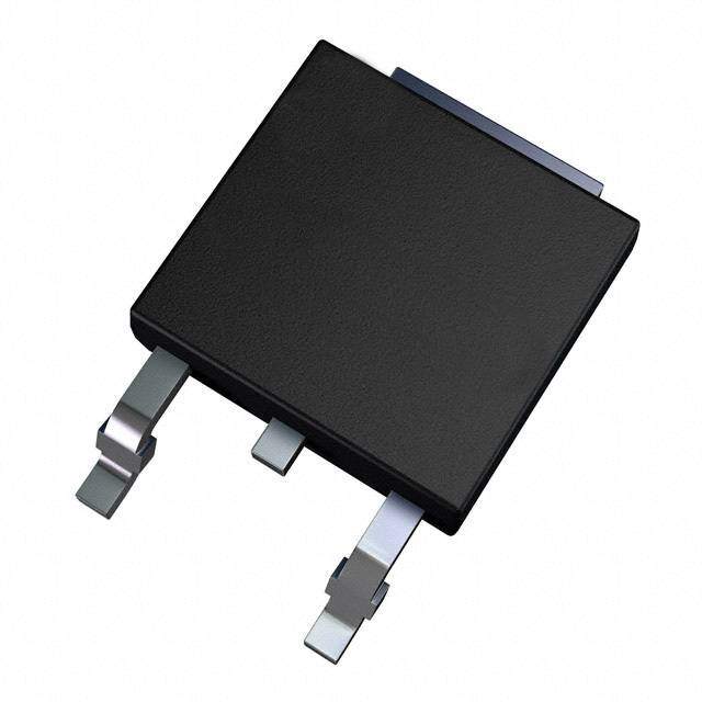
| 产品图片 |
|
| rohs | 符合RoHS无铅 / 符合限制有害物质指令(RoHS)规范要求 |
| 产品系列 | 电源管理 IC,低压差稳压器,Texas Instruments TLV1117-50CKVURG3- |
| 数据手册 | |
| 产品型号 | TLV1117-50CKVURG3 |
| 产品种类 | 低压差稳压器 |
| 供应商器件封装 | TO-252-3 |
| 其它名称 | 296-31968-6 |
| 包装 | Digi-Reel® |
| 单位重量 | 328.800 mg |
| 商标 | Texas Instruments |
| 回动电压—最大值 | 1.3 V at 100 mA/1.35 V at 500 mA/1.4 V at 800 mA |
| 安装类型 | 表面贴装 |
| 安装风格 | SMD/SMT |
| 封装 | Reel |
| 封装/外壳 | TO-252-3,DPak(2 引线+接片),SC-63 |
| 封装/箱体 | TO-252-3 |
| 工作温度 | 0°C ~ 125°C |
| 工厂包装数量 | 2500 |
| 最大工作温度 | + 125 C |
| 最大输入电压 | 15 V |
| 最小工作温度 | 0 C |
| 最小输入电压 | + 6.4 V |
| 标准包装 | 1 |
| 电压-跌落(典型值) | 1.2V @ 800mA |
| 电压-输入 | 6.4 V ~ 15 V |
| 电压-输出 | 5V |
| 电流-输出 | 800mA |
| 电流-限制(最小值) | 800mA |
| 稳压器拓扑 | 正,固定式 |
| 稳压器数 | 1 |
| 系列 | TLV1117-50 |
| 线路调整率 | 0.2 % |
| 负载调节 | 0.4 % |
| 输入偏压电流—最大 | 5 mA |
| 输出电压 | 5 V |
| 输出电流 | 800 mA |
| 输出端数量 | 1 Output |
| 输出类型 | Fixed |


- 商务部:美国ITC正式对集成电路等产品启动337调查
- 曝三星4nm工艺存在良率问题 高通将骁龙8 Gen1或转产台积电
- 太阳诱电将投资9.5亿元在常州建新厂生产MLCC 预计2023年完工
- 英特尔发布欧洲新工厂建设计划 深化IDM 2.0 战略
- 台积电先进制程称霸业界 有大客户加持明年业绩稳了
- 达到5530亿美元!SIA预计今年全球半导体销售额将创下新高
- 英特尔拟将自动驾驶子公司Mobileye上市 估值或超500亿美元
- 三星加码芯片和SET,合并消费电子和移动部门,撤换高东真等 CEO
- 三星电子宣布重大人事变动 还合并消费电子和移动部门
- 海关总署:前11个月进口集成电路产品价值2.52万亿元 增长14.8%


PDF Datasheet 数据手册内容提取
Product Sample & Technical Tools & Support & Folder Buy Documents Software Community TLV1117 SLVS561L–DECEMBER2004–REVISEDOCTOBER2014 TLV1117 Adjustable and Fixed Low-Dropout Voltage Regulator 1 Features 3 Description • 1.5-V,1.8-V,2.5-V,3.3-V,5-V,and The TLV1117 device is a positive low-dropout voltage 1 regulator designed to provide up to 800 mA of output Adjustable-OutputVoltageOptions current. The device is available in 1.5-V, 1.8-V, 2.5-V, • OutputCurrentof800mA 3.3-V, 5-V, and adjustable-output voltage options. All • SpecifiedDropoutVoltageatMultiple internal circuitry is designed to operate down to 1-V CurrentLevels input-to-output differential. Dropout voltage is specified at a maximum of 1.3 V at 800 mA, • 0.2%LineRegulationMaximum decreasingatlowerloadcurrents. • 0.4%LoadRegulationMaximum DeviceInformation 2 Applications ORDERNUMBER PACKAGE(PIN) BODYSIZE • ElectronicPointsofSale TLV1117DCY SOT-223(4) 6.50mm×3.50mm • Medical,Health,andFitnessApplications TLV1117DRJ SON(8) 4.00mm×4.00mm • Printers TLV1117KVU TO-252(3) 6.60mm×6.10mm • AppliancesandWhiteGoods TLV1117KCS TO-220(3) 10.16mm×8.70mm • TVSet-TopBoxes TLV1117KCT TO-220(3) 10.16mm×8.59mm DDPAK, TLV1117KTT 10.18mm×8.41mm TO-263(3) 4 Simplified Schematic TLV1117-ADJ INPUT OUTPUT ADJ/GND 1 An IMPORTANT NOTICE at the end of this data sheet addresses availability, warranty, changes, use in safety-critical applications, intellectualpropertymattersandotherimportantdisclaimers.PRODUCTIONDATA.
TLV1117 SLVS561L–DECEMBER2004–REVISEDOCTOBER2014 www.ti.com Table of Contents 1 Features.................................................................. 1 8.1 Overview.................................................................10 2 Applications........................................................... 1 8.2 FunctionalBlockDiagram.......................................10 3 Description............................................................. 1 8.3 FeatureDescription.................................................10 8.4 DeviceFunctionalModes........................................10 4 SimplifiedSchematic............................................. 1 9 ApplicationandImplementation........................ 12 5 RevisionHistory..................................................... 2 9.1 TypicalApplication .................................................12 6 PinConfigurationandFunctions......................... 3 10 PowerSupplyRecommendations..................... 13 7 Specifications......................................................... 4 11 Layout................................................................... 13 7.1 AbsoluteMaximumRatings .....................................4 11.1 LayoutGuidelines.................................................13 7.2 HandlingRatings......................................................4 11.2 LayoutExample....................................................13 7.3 RecommendedOperatingConditions.......................4 12 DeviceandDocumentationSupport................. 14 7.4 ThermalInformation..................................................5 7.5 TLV1117CElectricalCharacteristics........................6 12.1 Trademarks...........................................................14 7.6 TLV1117IElectricalCharacteristics..........................7 12.2 ElectrostaticDischargeCaution............................14 7.7 TypicalCharacteristics..............................................8 12.3 Glossary................................................................14 8 DetailedDescription............................................ 10 13 Mechanical,Packaging,andOrderable Information........................................................... 14 ChangesfromRevisionK(April2013)toRevisionL Page • UpdateddatasheettonewTIstandards–nospecificationchanges................................................................................... 1 • DeletedOrderingInformationtable. ...................................................................................................................................... 1 • AddedApplications................................................................................................................................................................. 1 • AddedDeviceandDocumentationSupportsection............................................................................................................. 14 • AddedMechanical,Packaging,andOrderableInformationsection..................................................................................... 14 5 Revision History ChangesfromRevisionJ(April2013)toRevisionK Page • Addedadditionalpackageoptions.......................................................................................................................................... 3 • AddedESDwarning............................................................................................................................................................. 14 2 SubmitDocumentationFeedback Copyright©2004–2014,TexasInstrumentsIncorporated ProductFolderLinks:TLV1117
TLV1117 www.ti.com SLVS561L–DECEMBER2004–REVISEDOCTOBER2014 6 Pin Configuration and Functions KTT (TO-263) PACKAGE KVU (TO-252) PACKAGE (TOPVIEW) (TOPVIEW) T 3 INPUT T 3 INPUT U U TP 2 OUTPUT TP 2 OUTPUT U U O 1 ADJ/GND O 1 ADJ/GND DCY(SOT-223) PACKAGE DRJ (QFN) PACKAGE KCT, KCS (TO-220) PACKAGE (TOPVIEW) (TOPVIEW) (TOPVIEW) T 3 INPUT U 3 INPUT ADJ/GND 1 8 NC TP 2 OUTPUT UT U 1 ADJ/GND O TP 2 OUTPUT VIN(1) 2 V 7 VOUT(2) U OUT O VIN(1) 3 6 VOUT(2) 1 ADJ/GND V (1) 4 5 V (2) IN OUT (1) VINpins(2, 3, 4) must be connected together. (2)VOUTpins (5, 6, 7) must be connected together. Table1.PinFunctions PIN TYPE DESCRIPTION NAME KTT KVU DCY DRJ KCT ADJ/GND 1 1 1 1 1 I/O Outputvoltageadjustmentpin.Connecttoaresistordivider. INPUT 3 3 3 2,3,4 3 I Voltageinput OUTPUT 2 2 2 5,6,7 2 O Voltageoutput NC - - - 8 - - Noconnect Copyright©2004–2014,TexasInstrumentsIncorporated SubmitDocumentationFeedback 3 ProductFolderLinks:TLV1117
TLV1117 SLVS561L–DECEMBER2004–REVISEDOCTOBER2014 www.ti.com 7 Specifications 7.1 Absolute Maximum Ratings(1) overoperatingfree-airtemperaturerange(unlessotherwisenoted) MIN MAX UNIT V Continuousinputvoltage 16 V IN T Operatingvirtual-junctiontemperature 150 °C J (1) StressesbeyondthoselistedunderAbsoluteMaximumRatingsmaycausepermanentdamagetothedevice.Thesearestressratings only,andfunctionaloperationofthedeviceattheseoranyotherconditionsbeyondthoseindicatedunderRecommendedOperating Conditionsisnotimplied.Exposuretoabsolute-maximum-ratedconditionsforextendedperiodsmayaffectdevicereliability. 7.2 Handling Ratings MIN MAX UNIT T Storagetemperaturerange –65 150 °C stg Humanbodymodel(HBM),perANSI/ESDA/JEDECJS-001,all pins(1) 0 2500 V Electrostaticdischarge V (ESD) Chargeddevicemodel(CDM),perJEDECspecification JESD22-C101,allpins(2) 0 1500 (1) JEDECdocumentJEP155statesthat500-VHBMallowssafemanufacturingwithastandardESDcontrolprocess. (2) JEDECdocumentJEP157statesthat250-VCDMallowssafemanufacturingwithastandardESDcontrolprocess. 7.3 Recommended Operating Conditions MIN(1) MAX UNIT TLV1117 2.7 15 TLV1117-15 2.9 15 TLV1117-18 3.2 15 V Inputvoltage V IN TLV1117-25 3.9 15 TLV1117-33 4.7 15 TLV1117-50 6.4 15 I Outputcurrent 0.8 A O TLV1117C 0 125 T Operatingvirtual-junctiontemperature °C J TLV1117I –40 125 (1) Theinput-to-outputdifferentialacrosstheregulatorshouldprovideforsomemarginagainstregulatoroperationatthemaximumdropout (foraparticularcurrentvalue).Thismarginisneededtoaccountfortolerancesinboththeinputvoltage(lowerlimit)andtheoutput voltage(upperlimit).TheabsoluteminimumV foradesiredmaximumoutputcurrentcanbecalculatedbythefollowing: IN V =V +V IN(min) OUT(max) DO(maxatratedcurrent) 4 SubmitDocumentationFeedback Copyright©2004–2014,TexasInstrumentsIncorporated ProductFolderLinks:TLV1117
TLV1117 www.ti.com SLVS561L–DECEMBER2004–REVISEDOCTOBER2014 7.4 Thermal Information TLV1117 THERMALMETRIC(1)(2)(3) PowerFlex UNITS KTE KTP DRJ DCY KVU KCS,KCT KTT (3PINS) (3PINS) (8PINS) (4PINS) (3PINS) (3PINS) (3PINS) Junction-to-ambientthermal R 38.6 49.2 38.3 104.3 50.9 30.1 27.5 θJA resistance Junction-to-case(top)thermal R 34.7 60.6 36.5 53.7 57.9 44.6 43.2 θJC(top) resistance R Junction-to-boardthermalresistance 3.2 3.1 60.5 5.7 34.8 1.2 17.3 θJB Junction-to-topcharacterization ψ 5.9 8.7 0.2 3.1 6 5 2.8 JT parameter °C/W Junction-to-boardcharacterization ψ 3.1 3 12 5.5 23.7 1.2 9.3 JB parameter Junction-to-case(bottom)thermal R 3 3 4.7 n/a 0.4 0.4 0.3 θJC(bot) resistance Thermalresistancebetweenthedie R junctionandthebottomofthe 2.7 1.4 1.78 n/a n/a 3 1.94 θJP exposedpad. (1) Formoreinformationabouttraditionalandnewthermalmetrics,seetheICPackageThermalMetricsapplicationreport,SPRA953. (2) ForthermalestimatesofthisdevicebasedonPCBcopperarea,seetheTIPCBThermalCalculator. (3) MaximumpowerdissipationisafunctionofT(max),θ ,andT .Themaximumallowablepowerdissipationatanyallowableambient J JA A temperatureisP =(T(max)–T )/θJ .OperatingattheabsolutemaximumT of150°Ccanaffectreliability. D J A A J Copyright©2004–2014,TexasInstrumentsIncorporated SubmitDocumentationFeedback 5 ProductFolderLinks:TLV1117
TLV1117 SLVS561L–DECEMBER2004–REVISEDOCTOBER2014 www.ti.com 7.5 TLV1117C Electrical Characteristics T =0°Cto125°C,alltypicalvaluesareatT =25°C(unlessotherwisenoted) J J PARAMETER TESTCONDITIONS(1) MIN TYP MAX UNIT V –V =2V,I =10mA,T =25°C 1.238 1.25 1.262 IN OUT OUT J Referencevoltage,V TLV1117 REF V –V =1.4Vto10V,I =10mAto800mA 1.225 1.25 1.27 IN OUT OUT V =3.5V,I =10mA,T =25°C 1.485 1.5 1.515 IN OUT J TLV1117-15 V =2.9Vto10V,I =0to800mA 1.455 1.5 1.545 IN OUT V =3.8V,I =10mA,T =25°C 1.782 1.8 1.818 IN OUT J TLV1117-18 V =3.2Vto10V,I =0to800mA 1.746 1.8 1.854 IN OUT V V =4.5V,I =10mA,T =25°C 2.475 2.5 2.525 IN OUT J Outputvoltage,V TLV1117-25 OUT V =3.9Vto10V,I =0to800mA 2.450 2.5 2.550 IN OUT V =5V,I =10mA,T =25°C 3.267 3.3 3.333 IN OUT J TLV1117-33 V =4.75Vto10V,I =0to800mA 3.235 3.3 3.365 IN OUT V =7V,I =10mA,T =25°C 4.950 5.0 5.050 IN OUT J TLV1117-50 V =6.5Vto12V,I =0to800mA 4.900 5.0 5.100 IN OUT I =10mA,V –V =1.5Vto13.75V TLV1117 0.035% 0.2% — OUT IN OUT I =0mA,V =2.9Vto10V TLV1117-15 1 6 OUT IN I =0mA,V =3.2Vto10V TLV1117-18 1 6 OUT IN Lineregulation I =0mA,V =3.9Vto10V TLV1117-25 1 6 mV OUT IN I =0mA,V =4.75Vto15V TLV1117-33 1 6 OUT IN I =0mA,V =6.5Vto15V TLV1117-50 1 10 OUT IN I =10mAto800mA,V –V =3V TLV1117 0.2% 0.4% — OUT IN OUT I =0to800mA,V =2.9V TLV1117-15 1 10 OUT IN I =0to800mA,V =3.2V TLV1117-18 1 10 OUT IN Loadregulation I =0to800mA,V =3.9V TLV1117-25 1 10 mV OUT IN I =0to800mA,V =4.75V TLV1117-33 1 10 OUT IN I =0to800mA,V =6.5V TLV1117-50 1 15 OUT IN I =100mA 1.1 1.2 OUT Dropoutvoltage,V (2) I =500mA 1.15 1.25 V DO OUT I =800mA 1.2 1.3 OUT Currentlimit V –V =5V,T =25°C(3) 0.8 1.2 1.6 A IN OUT J Minimumloadcurrent V =15V TLV1117 1.7 5 mA IN Allfixed-voltage Quiescentcurrent V ≤15V 5 10 mA IN options Thermalregulation 30-mspulse,T =25°C 0.01 0.1 %/W A Ripplerejection V –V =3V,V =1V ,f=120Hz 60 75 dB IN OUT ripple pp ADJpincurrent 80 120 μA ChangeinADJpincurrent V –V =1.4Vto10V,I =10mAto800mA 0.2 5 μA IN OUT OUT Temperaturestability T =fullrange 0.5% — J Long-termstability 1000hrs,Noload,T =125°C 0.3% — A Outputnoisevoltage f=10Hzto100kHz 0.003% — (%ofV ) OUT (1) Allcharacteristicsaremeasuredwitha10-μFcapacitoracrosstheinputanda10-μFcapacitoracrosstheoutput.Pulsetesting techniquesareusedtomaintainthejunctiontemperatureasclosetotheambienttemperatureaspossible. (2) DropoutisdefinedastheV toV differentialatwhichV drops100mVbelowthevalueofV , IN OUT OUT OUT measuredatV =V +1.5V. IN OUT(nom) (3) Currentlimittestspecifiedunderrecommendedoperatingconditions. 6 SubmitDocumentationFeedback Copyright©2004–2014,TexasInstrumentsIncorporated ProductFolderLinks:TLV1117
TLV1117 www.ti.com SLVS561L–DECEMBER2004–REVISEDOCTOBER2014 7.6 TLV1117I Electrical Characteristics T =–40°Cto125°C,alltypicalvaluesareatT =25°C(unlessotherwisenoted) J J PARAMETER TESTCONDITIONS(1) MIN TYP MAX UNIT V –V =2V,I =10mA,T =25°C 1.238 1.25 1.262 IN OUT OUT J Referencevoltage,V TLV1117 REF V –V =1.4Vto10V,I =10mAto800mA 1.200 1.25 1.29 IN OUT OUT V =3.5V,I =10mA,T =25°C 1.485 1.5 1.515 IN OUT J TLV1117-15 V =2.9Vto10V,I =0to800mA 1.44 1.5 1.56 IN OUT V =3.8V,I =10mA,T =25°C 1.782 1.8 1.818 IN OUT J TLV1117-18 V =3.2Vto10V,I =0to800mA 1.728 1.8 1.872 IN OUT V V =4.5V,I =10mA,T =25°C 2.475 2.5 2.525 IN OUT J Outputvoltage,V TLV1117-25 OUT V =3.9Vto10V,I =0to800mA 2.4 2.5 2.6 IN OUT V =5V,I =10mA,T =25°C 3.267 3.3 3.333 IN OUT J TLV1117-33 V =4.75Vto10V,I =0to800mA 3.168 3.3 3.432 IN OUT V =7V,I =10mA,T =25°C 4.95 5.0 5.05 IN OUT J TLV1117-50 V =6.5Vto12V,I =0to800mA 4.80 5.0 5.20 IN OUT I =10mA,V –V =1.5Vto13.75V TLV1117 0.035% 0.3% — OUT IN OUT I =0mA,V =2.9Vto10V TLV1117-15 1 10 OUT IN I =0mA,V =3.2Vto10V TLV1117-18 1 10 OUT IN Lineregulation I =0mA,V =3.9Vto10V TLV1117-25 1 10 mV OUT IN I =0mA,V =4.75Vto15V TLV1117-33 1 10 OUT IN I =0mA,V =6.5Vto15V TLV1117-50 1 15 OUT IN I =10mAto800mA,V –V =3V TLV1117 0.2% 0.5% — OUT IN OUT I =0to800mA,V =2.9V TLV1117-15 1 15 OUT IN I =0to800mA,V =3.2V TLV1117-18 1 15 OUT IN Loadregulation I =0to800mA,V =3.9V TLV1117-25 1 15 mV OUT IN I =0to800mA,V =4.75V TLV1117-33 1 15 OUT IN I =0to800mA,V =6.5V TLV1117-50 1 20 OUT IN I =100mA 1.1 1.3 OUT Dropoutvoltage,V (2) I =500mA 1.15 1.35 V DO OUT I =800mA 1.2 1.4 OUT Currentlimit V –V =5V,T =25°C(3) 0.8 1.2 1.6 A IN OUT J Minimumloadcurrent V =15V TLV1117 1.7 5 mA IN Allfixed-voltage Quiescentcurrent V ≤15V 5 15 mA IN options Thermalregulation 30-mspulse,T =25°C 0.01 0.1 %/W A Ripplerejection V –V =3V,V =1V ,f=120Hz 60 75 dB IN OUT ripple pp ADJpincurrent 80 120 μA ChangeinADJpincurrent V –V =1.4Vto10V,I =10mAto800mA 0.2 10 μA IN OUT OUT Temperaturestability T =fullrange 0.5% — J Long-termstability 1000hrs,Noload,T =125°C 0.3% — A Outputnoisevoltage f=10Hzto100kHz 0.003% — (%ofV ) OUT (1) Allcharacteristicsaremeasuredwitha10-μFcapacitoracrosstheinputanda10-μFcapacitoracrosstheoutput.Pulsetesting techniquesareusedtomaintainthejunctiontemperatureasclosetotheambienttemperatureaspossible. (2) DropoutisdefinedastheV toV differentialatwhichV drops100mVbelowthevalueofV , IN OUT OUT OUT measuredatV =V +1.5V. IN OUT(nom) (3) Currentlimittestspecifiedunderrecommendedoperatingconditions Copyright©2004–2014,TexasInstrumentsIncorporated SubmitDocumentationFeedback 7 ProductFolderLinks:TLV1117
TLV1117 SLVS561L–DECEMBER2004–REVISEDOCTOBER2014 www.ti.com 7.7 Typical Characteristics 1.8 0 TJ = 25(cid:1)C (cid:1)Load = 800 mA 1.6 −0.05 nt (A) 1.4 TJ = 125(cid:1)C −0.1 e 1.2 Circuit Curr 0.81 (cid:1)V (%)OUT−−0.01.52 ort- h 0.6 S −0.25 0.4 −0.3 0.2 0 −0.35 0 3 6 9 12 15 −50 −25 0 25 50 75 100 125 Input/Output Differential (V) Temperature ((cid:1)C) Figure1.Short-CircuitCurrentvs(V –V ) IN OUT Figure2.LoadRegulation 80 90 70 80 f = 120 Hz 70 60 ection (dB) 4500 ection (dB) 5600 Rej Rej 40 Ripple 30 Ripple 30 20 20 10 10 0 0 10 100 1k 10k 100k 0 200 400 600 800 Frequency (Hz) Load (mA) Figure3.RippleRejectionvsFrequency(ADJVersion) Figure4.RippleRejectionvsLoadCurrent(ADJVersion) 2 150 1.5 140 130 %) 1 ge Variation ( 0.50 (cid:1)Current (A) 111200 olta Pin 100 put V −0.5 ADJ 90 Out −1 80 −1.5 70 −2 60 −50 −25 0 25 50 75 100 125 150 −50 −25 0 25 50 75 100 125 150 Temperature ((cid:1)C) Temperature ((cid:1)C) Figure5.TemperatureStability Figure6.ADJPinCurrentvsTemperature 8 SubmitDocumentationFeedback Copyright©2004–2014,TexasInstrumentsIncorporated ProductFolderLinks:TLV1117
TLV1117 www.ti.com SLVS561L–DECEMBER2004–REVISEDOCTOBER2014 Typical Characteristics (continued) 0.2 2.6 100 7 2.4 90 Input Voltage 0.1 2.2 80 6 Output-Voltage Deviation 2 Output Voltage Deviation (V) −−−000...0321 CCVPrIIONNeU l==oT a41=d.0 81 = (cid:1)0V F-0(cid:1).F1 ATLaonatda lCuumrrent 00011111.......4682468 Load Current (A) Output Voltage Deviation (mV) 12345670000000 CCIOIOUNUT =T = 0= 0. 11.1 0(cid:1) -AF(cid:1)F TaOnutatpluumt-Voltage Deviation 345 Input Voltage (V) 0 2 −0.4 0.2 0 −10 −0.5 −0.2 −20 1 −60 −40 −20 0 20 −40 −20 0 20 40 60 80 100 120 140 Time ((cid:1)s) Time ((cid:1)s) Figure7.TLV1117-33LoadTransientResponse Figure8.TLV1117-33LineTransientResponse Copyright©2004–2014,TexasInstrumentsIncorporated SubmitDocumentationFeedback 9 ProductFolderLinks:TLV1117
TLV1117 SLVS561L–DECEMBER2004–REVISEDOCTOBER2014 www.ti.com 8 Detailed Description 8.1 Overview The TLV1117 device is a positive low-dropout voltage regulator designed to provide up to 800 mA of output current. The device is available in 1.5-V, 1.8-V, 2.5-V, 3.3-V, 5-V, and adjustable-output voltage options. All internal circuitry is designed to operate down to 1-V input-to-output differential. Dropout voltage is specified at a maximumof1.3Vat800mA,decreasingatlowerloadcurrents. The TLV1117 device is designed to be stable with tantalum and aluminum electrolytic output capacitors having anESRbetween0.2Ω and10Ω. Unlike pnp-type regulators, in which up to 10% of the output current is wasted as quiescent current, the quiescentcurrentoftheTLV1117deviceflowsintotheload,increasingefficiency. The TLV1117C device is characterized for operation over the virtual junction temperature range of 0°C to 125°C, and the TLV1117I device is characterized for operation over the virtual junction temperature range of –40°C to 125°C. 8.2 Functional Block Diagram FunctionalBlockDiagram 80!A INPUT + Overload 5mA 1.25V Block OUTPUT ADJUST 8.3 Feature Description 8.3.1 NPNOutputDrive NPN output topology provides lower output impedance than most LDOs. However, an output capacitor is required. To support maximum current and lowest temperature, 1.4-V headroom is recommended (less for lower currents)(V –V ). I O 8.3.2 OverloadBlock Currentlimitingandovertemperatureshutdownprotectsagainstoverloadorunderheatsinking. 8.3.3 ProgrammableFeedback Op amp with 1.25-V offset input at the ADJUST pin provides easy output voltage programming. For current regulationapplications,asingleresistorwhoseresistancevalueis1.25V/IOUTandpowerratingisgreaterthan (1.25V)2/Rshouldbeused.Forvoltageregulationapplications,tworesistorssettheoutputvoltage. 8.4 Device Functional Modes 8.4.1 Normaloperation The device OUTPUT pin will source current necessary to make OUTPUT pin 1.25 V greater than ADJUST terminaltoprovideoutputregulation. 10 SubmitDocumentationFeedback Copyright©2004–2014,TexasInstrumentsIncorporated ProductFolderLinks:TLV1117
TLV1117 www.ti.com SLVS561L–DECEMBER2004–REVISEDOCTOBER2014 Device Functional Modes (continued) 8.4.2 OperationWithLowInputVoltage The adjustable version of the device requires 1-V headroom (V – V ) to operate in regulation. With less I O headroom,thedevicemaydropoutandOUTPUTvoltagewillbeINPUTvoltageminusdropoutvoltage. 8.4.3 OperationatLightLoads The device passes its bias current to the OUTPUT pin. The load or feedback must consume this minimum currentforregulationortheoutputmaybetoohigh. 8.4.4 OperationinSelfProtection When an overload occurs the device will shut down the output stage or reduce the output current to prevent device damage. The device will automatically reset from the overload. The output may be reduced or alternate betweenonandoffuntiltheoverloadisremoved. Copyright©2004–2014,TexasInstrumentsIncorporated SubmitDocumentationFeedback 11 ProductFolderLinks:TLV1117
TLV1117 SLVS561L–DECEMBER2004–REVISEDOCTOBER2014 www.ti.com 9 Application and Implementation NOTE Information in the following applications sections is not part of the TI component specification, and TI does not warrant its accuracy or completeness. TI’s customers are responsible for determining suitability of components for their purposes. Customers should validateandtesttheirdesignimplementationtoconfirmsystemfunctionality. 9.1 Typical Application 1N4002 (See Note D) TLV1117−ADJ VI INPUT OUTPUT VO ADJ/GND 10µF IADJ VREF R1 (see Note C) 100µF (see NoteA) CADJ R2 (see Note B) Figure9. BasicAdjustableRegulator The adjustable version of the TLV1117 will take a 2.7 to 15-V input. The voltage V refers to the voltage REF between the output and the ADJUST pin, typically 1.25 V. The V voltage causes a current to flow across R1, REF which is the same current that will flow across R2 (minus the negligible 50-µA I ). Therefore, R2 can be ADJ adjusted to create a larger voltage drop from GND and set the output voltage. The output voltage equation is describedinDetailedDesignProcedure. 9.1.1 DesignRequirements • (A) Output capacitor selection is critical for regulator stability. Larger C values benefit the regulator by OUT improving transient response and loop stability. This device is designed to be stable with tantalum and aluminumelectrolyticoutputcapacitorshavinganESRbetween0.2 Ω and10Ω. • (B) C can be used to improve ripple rejection. If C is used, a C that is larger in value than C must ADJ ADJ OUT ADJ beused. • (C)C isrecommendedifTLV1117deviceisnotlocatednearthepower-supplyfilter. IN • (D)AnexternaldiodeisrecommendedtoprotecttheregulatoriftheinputinstantaneouslyisshortedtoGND. 9.1.2 DetailedDesignProcedure TheoutputvoltagecanbecalculatedasshowninFigure10: § R2· (cid:11) (cid:12) V V ¨1(cid:14) ¸(cid:14) I uR2 OUT REF ADJ © R1¹ Figure10. I canbeneglectedinmostapplicationsbecauseitsvalueisapproximately80 µA. ADJ 12 SubmitDocumentationFeedback Copyright©2004–2014,TexasInstrumentsIncorporated ProductFolderLinks:TLV1117
TLV1117 www.ti.com SLVS561L–DECEMBER2004–REVISEDOCTOBER2014 Typical Application (continued) 9.1.3 ApplicationCurves 1.4 1.2 TJ = 25(cid:1)C 1 V) e ( oltag 0.8 TJ = 125(cid:1)C V ut 0.6 o p o Dr 0.4 0.2 0 0 100 200 300 400 500 600 700 800 Load Current (mA) Figure11.DropoutVoltagevsLoadCurrent 10 Power Supply Recommendations The fixed and adjustable versions of the TLV1117 have different recommended ranges of operating voltage. RefertoRecommendedOperatingConditionsforspecificoperatingranges. 11 Layout 11.1 Layout Guidelines One or two input capacitors are recommended if the TLV1117 is not located near its power supply output filter capacitor. These capacitors can filter high-frequency noise and mitigate brief voltage surges from the input. Traces on the input and output pins of the device should be wide enough to support the full range of current neededintheapplicationtominimizeI×Rdrop. 11.2 Layout Example C OUTPUT OUT d n u o Gr R2 Power C R1 ADJ/GND OUTPUT INPUT (cid:20)(cid:19)(cid:19)PF adj Ground Figure12. LayoutExample Copyright©2004–2014,TexasInstrumentsIncorporated SubmitDocumentationFeedback 13 ProductFolderLinks:TLV1117
TLV1117 SLVS561L–DECEMBER2004–REVISEDOCTOBER2014 www.ti.com 12 Device and Documentation Support 12.1 Trademarks Alltrademarksarethepropertyoftheirrespectiveowners. 12.2 Electrostatic Discharge Caution Thesedeviceshavelimitedbuilt-inESDprotection.Theleadsshouldbeshortedtogetherorthedeviceplacedinconductivefoam duringstorageorhandlingtopreventelectrostaticdamagetotheMOSgates. 12.3 Glossary SLYZ022—TIGlossary. Thisglossarylistsandexplainsterms,acronymsanddefinitions. 13 Mechanical, Packaging, and Orderable Information The following pages include mechanical packaging and orderable information. This information is the most current data available for the designated devices. This data is subject to change without notice and revision of thisdocument.Forbrowserbasedversionsofthisdatasheet,refertothelefthandnavigation. 14 SubmitDocumentationFeedback Copyright©2004–2014,TexasInstrumentsIncorporated ProductFolderLinks:TLV1117
PACKAGE OPTION ADDENDUM www.ti.com 6-Feb-2020 PACKAGING INFORMATION Orderable Device Status Package Type Package Pins Package Eco Plan Lead/Ball Finish MSL Peak Temp Op Temp (°C) Device Marking Samples (1) Drawing Qty (2) (6) (3) (4/5) TLV1117-15CDCY ACTIVE SOT-223 DCY 4 80 Green (RoHS SN Level-2-260C-1 YEAR 0 to 125 T2 & no Sb/Br) TLV1117-15CDCYR ACTIVE SOT-223 DCY 4 2500 Green (RoHS SN Level-2-260C-1 YEAR 0 to 125 T2 & no Sb/Br) TLV1117-15CDCYRG3 ACTIVE SOT-223 DCY 4 2500 Green (RoHS SN Level-2-260C-1 YEAR 0 to 125 T2 & no Sb/Br) TLV1117-15CDRJR ACTIVE SON DRJ 8 3000 Green (RoHS NIPDAU Level-2-260C-1 YEAR 0 to 125 ZYH & no Sb/Br) TLV1117-15IDCY ACTIVE SOT-223 DCY 4 80 Green (RoHS SN Level-2-260C-1 YEAR -40 to 125 T3 & no Sb/Br) TLV1117-15IDCYR ACTIVE SOT-223 DCY 4 2500 Green (RoHS SN Level-2-260C-1 YEAR -40 to 125 T3 & no Sb/Br) TLV1117-15IKVURG3 ACTIVE TO-252 KVU 3 2500 Green (RoHS SN Level-3-260C-168 HR -40 to 125 ZF15 & no Sb/Br) TLV1117-18CDCY ACTIVE SOT-223 DCY 4 80 Green (RoHS SN Level-2-260C-1 YEAR 0 to 125 T4 & no Sb/Br) TLV1117-18CDCYR ACTIVE SOT-223 DCY 4 2500 Green (RoHS SN Level-2-260C-1 YEAR 0 to 125 T4 & no Sb/Br) TLV1117-18CDCYRG3 ACTIVE SOT-223 DCY 4 2500 Green (RoHS SN Level-2-260C-1 YEAR 0 to 125 T4 & no Sb/Br) TLV1117-18CDRJR ACTIVE SON DRJ 8 3000 Green (RoHS NIPDAU Level-2-260C-1 YEAR 0 to 125 ZYK & no Sb/Br) TLV1117-18CKVURG3 ACTIVE TO-252 KVU 3 2500 Green (RoHS SN Level-3-260C-168 HR 0 to 125 ZE18 & no Sb/Br) TLV1117-18IDCY ACTIVE SOT-223 DCY 4 80 Green (RoHS SN Level-2-260C-1 YEAR -40 to 125 T5 & no Sb/Br) TLV1117-18IDCYR ACTIVE SOT-223 DCY 4 2500 Green (RoHS SN Level-2-260C-1 YEAR -40 to 125 T5 & no Sb/Br) TLV1117-18IDCYRG3 ACTIVE SOT-223 DCY 4 2500 Green (RoHS SN Level-2-260C-1 YEAR -40 to 125 T5 & no Sb/Br) TLV1117-18IDRJR ACTIVE SON DRJ 8 1000 Green (RoHS NIPDAU Level-2-260C-1 YEAR -40 to 125 ZYL & no Sb/Br) TLV1117-18IKVURG3 ACTIVE TO-252 KVU 3 2500 Green (RoHS SN Level-3-260C-168 HR -40 to 125 ZF18 & no Sb/Br) Addendum-Page 1
PACKAGE OPTION ADDENDUM www.ti.com 6-Feb-2020 Orderable Device Status Package Type Package Pins Package Eco Plan Lead/Ball Finish MSL Peak Temp Op Temp (°C) Device Marking Samples (1) Drawing Qty (2) (6) (3) (4/5) TLV1117-25CDCY ACTIVE SOT-223 DCY 4 80 Green (RoHS SN Level-2-260C-1 YEAR 0 to 125 T6 & no Sb/Br) TLV1117-25CDCYR ACTIVE SOT-223 DCY 4 2500 Green (RoHS SN Level-2-260C-1 YEAR 0 to 125 T6 & no Sb/Br) TLV1117-25CDCYRG3 ACTIVE SOT-223 DCY 4 2500 Green (RoHS SN Level-2-260C-1 YEAR 0 to 125 T6 & no Sb/Br) TLV1117-25CKVURG3 ACTIVE TO-252 KVU 3 2500 Green (RoHS SN Level-3-260C-168 HR 0 to 125 ZE25 & no Sb/Br) TLV1117-25IDCY ACTIVE SOT-223 DCY 4 80 Green (RoHS SN Level-2-260C-1 YEAR -40 to 125 T8 & no Sb/Br) TLV1117-25IDCYR ACTIVE SOT-223 DCY 4 2500 Green (RoHS SN Level-2-260C-1 YEAR -40 to 125 T8 & no Sb/Br) TLV1117-25IDRJR ACTIVE SON DRJ 8 3000 Green (RoHS NIPDAU Level-2-260C-1 YEAR -40 to 125 ZYN & no Sb/Br) TLV1117-33CDCY ACTIVE SOT-223 DCY 4 80 Green (RoHS SN Level-2-260C-1 YEAR 0 to 125 V3 & no Sb/Br) TLV1117-33CDCYG3 ACTIVE SOT-223 DCY 4 80 Green (RoHS SN Level-2-260C-1 YEAR 0 to 125 V3 & no Sb/Br) TLV1117-33CDCYR ACTIVE SOT-223 DCY 4 2500 Green (RoHS SN Level-2-260C-1 YEAR 0 to 125 V3 & no Sb/Br) TLV1117-33CDCYRG3 ACTIVE SOT-223 DCY 4 2500 Green (RoHS SN Level-2-260C-1 YEAR 0 to 125 V3 & no Sb/Br) TLV1117-33CDRJR ACTIVE SON DRJ 8 1000 Green (RoHS NIPDAU Level-2-260C-1 YEAR 0 to 125 ZYP & no Sb/Br) TLV1117-33CKVURG3 ACTIVE TO-252 KVU 3 2500 Green (RoHS SN Level-3-260C-168 HR 0 to 125 ZE33 & no Sb/Br) TLV1117-33IDCY ACTIVE SOT-223 DCY 4 80 Green (RoHS SN Level-2-260C-1 YEAR -40 to 125 (V3, VS) & no Sb/Br) TLV1117-33IDCYG3 ACTIVE SOT-223 DCY 4 80 Green (RoHS SN Level-2-260C-1 YEAR -40 to 125 (V3, VS) & no Sb/Br) TLV1117-33IDCYR ACTIVE SOT-223 DCY 4 2500 Green (RoHS SN Level-2-260C-1 YEAR -40 to 125 VS & no Sb/Br) TLV1117-33IDCYRG3 ACTIVE SOT-223 DCY 4 2500 Green (RoHS SN Level-2-260C-1 YEAR -40 to 125 VS & no Sb/Br) TLV1117-33IDRJR ACTIVE SON DRJ 8 1000 Green (RoHS NIPDAU Level-2-260C-1 YEAR -40 to 125 ZYR & no Sb/Br) Addendum-Page 2
PACKAGE OPTION ADDENDUM www.ti.com 6-Feb-2020 Orderable Device Status Package Type Package Pins Package Eco Plan Lead/Ball Finish MSL Peak Temp Op Temp (°C) Device Marking Samples (1) Drawing Qty (2) (6) (3) (4/5) TLV1117-33IKVURG3 ACTIVE TO-252 KVU 3 2500 Green (RoHS SN Level-3-260C-168 HR -40 to 125 ZF33 & no Sb/Br) TLV1117-50CDCY ACTIVE SOT-223 DCY 4 80 Green (RoHS SN Level-2-260C-1 YEAR 0 to 125 VT & no Sb/Br) TLV1117-50CDCYG3 ACTIVE SOT-223 DCY 4 80 Green (RoHS SN Level-2-260C-1 YEAR 0 to 125 VT & no Sb/Br) TLV1117-50CDCYR ACTIVE SOT-223 DCY 4 2500 Green (RoHS SN Level-2-260C-1 YEAR 0 to 125 VT & no Sb/Br) TLV1117-50CDCYRG3 ACTIVE SOT-223 DCY 4 2500 Green (RoHS SN Level-2-260C-1 YEAR 0 to 125 VT & no Sb/Br) TLV1117-50CDRJR ACTIVE SON DRJ 8 3000 Green (RoHS NIPDAU Level-2-260C-1 YEAR 0 to 125 ZE50 & no Sb/Br) TLV1117-50CKVURG3 ACTIVE TO-252 KVU 3 2500 Green (RoHS SN Level-3-260C-168 HR 0 to 125 ZE50 & no Sb/Br) TLV1117-50IDCY ACTIVE SOT-223 DCY 4 80 Green (RoHS SN Level-2-260C-1 YEAR -40 to 125 VU & no Sb/Br) TLV1117-50IDCYR ACTIVE SOT-223 DCY 4 2500 Green (RoHS SN Level-2-260C-1 YEAR -40 to 125 VU & no Sb/Br) TLV1117-50IDCYRG3 ACTIVE SOT-223 DCY 4 2500 Green (RoHS SN Level-2-260C-1 YEAR -40 to 125 VU & no Sb/Br) TLV1117-50IDRJR ACTIVE SON DRJ 8 1000 Green (RoHS NIPDAU Level-2-260C-1 YEAR -40 to 125 ZF50 & no Sb/Br) TLV1117-50IDRJRG4 ACTIVE SON DRJ 8 1000 Green (RoHS NIPDAU Level-2-260C-1 YEAR -40 to 125 ZF50 & no Sb/Br) TLV1117-50IKVURG3 ACTIVE TO-252 KVU 3 2500 Green (RoHS SN Level-3-260C-168 HR -40 to 125 ZF50 & no Sb/Br) TLV1117CDCY ACTIVE SOT-223 DCY 4 80 Green (RoHS SN Level-2-260C-1 YEAR 0 to 125 V4 & no Sb/Br) TLV1117CDCYG3 ACTIVE SOT-223 DCY 4 80 Green (RoHS SN Level-2-260C-1 YEAR 0 to 125 V4 & no Sb/Br) TLV1117CDCYR ACTIVE SOT-223 DCY 4 2500 Green (RoHS SN Level-2-260C-1 YEAR 0 to 125 V4 & no Sb/Br) TLV1117CDCYRG3 ACTIVE SOT-223 DCY 4 2500 Green (RoHS SN Level-2-260C-1 YEAR 0 to 125 V4 & no Sb/Br) TLV1117CDRJR ACTIVE SON DRJ 8 1000 Green (RoHS NIPDAU Level-2-260C-1 YEAR 0 to 125 ZYS & no Sb/Br) Addendum-Page 3
PACKAGE OPTION ADDENDUM www.ti.com 6-Feb-2020 Orderable Device Status Package Type Package Pins Package Eco Plan Lead/Ball Finish MSL Peak Temp Op Temp (°C) Device Marking Samples (1) Drawing Qty (2) (6) (3) (4/5) TLV1117CKCS ACTIVE TO-220 KCS 3 50 Pb-Free SN N / A for Pkg Type 0 to 125 TLV1117C (RoHS) TLV1117CKCT ACTIVE TO-220 KCT 3 50 Pb-Free SN N / A for Pkg Type 0 to 125 TLV1117C (RoHS) TLV1117CKTTR ACTIVE DDPAK/ KTT 3 500 Green (RoHS SN Level-3-245C-168 HR 0 to 125 TLV1117C TO-263 & no Sb/Br) TLV1117CKTTRG3 ACTIVE DDPAK/ KTT 3 500 Green (RoHS SN Level-3-245C-168 HR 0 to 125 TLV1117C TO-263 & no Sb/Br) TLV1117CKVURG3 ACTIVE TO-252 KVU 3 2500 Green (RoHS SN Level-3-260C-168 HR 0 to 125 TV1117 & no Sb/Br) TLV1117IDCY ACTIVE SOT-223 DCY 4 80 Green (RoHS SN Level-2-260C-1 YEAR -40 to 125 V2 & no Sb/Br) TLV1117IDCYG3 ACTIVE SOT-223 DCY 4 80 Green (RoHS SN Level-2-260C-1 YEAR -40 to 125 V2 & no Sb/Br) TLV1117IDCYR ACTIVE SOT-223 DCY 4 2500 Green (RoHS SN Level-2-260C-1 YEAR -40 to 125 V2 & no Sb/Br) TLV1117IDCYRG3 ACTIVE SOT-223 DCY 4 2500 Green (RoHS SN Level-2-260C-1 YEAR -40 to 125 V2 & no Sb/Br) TLV1117IDRJR ACTIVE SON DRJ 8 1000 Green (RoHS NIPDAU Level-2-260C-1 YEAR -40 to 125 ZYT & no Sb/Br) TLV1117IKCS ACTIVE TO-220 KCS 3 50 Pb-Free SN N / A for Pkg Type -40 to 125 TLV1117I (RoHS) TLV1117IKCSE3 ACTIVE TO-220 KCS 3 50 Pb-Free SN N / A for Pkg Type -40 to 125 TLV1117I (RoHS) TLV1117IKTTR ACTIVE DDPAK/ KTT 3 500 Green (RoHS SN Level-3-245C-168 HR -40 to 125 TLV1117I TO-263 & no Sb/Br) TLV1117IKVURG3 ACTIVE TO-252 KVU 3 2500 Green (RoHS SN Level-3-260C-168 HR -40 to 125 TY1117 & no Sb/Br) (1) The marketing status values are defined as follows: ACTIVE: Product device recommended for new designs. LIFEBUY: TI has announced that the device will be discontinued, and a lifetime-buy period is in effect. NRND: Not recommended for new designs. Device is in production to support existing customers, but TI does not recommend using this part in a new design. PREVIEW: Device has been announced but is not in production. Samples may or may not be available. OBSOLETE: TI has discontinued the production of the device. Addendum-Page 4
PACKAGE OPTION ADDENDUM www.ti.com 6-Feb-2020 (2) RoHS: TI defines "RoHS" to mean semiconductor products that are compliant with the current EU RoHS requirements for all 10 RoHS substances, including the requirement that RoHS substance do not exceed 0.1% by weight in homogeneous materials. Where designed to be soldered at high temperatures, "RoHS" products are suitable for use in specified lead-free processes. TI may reference these types of products as "Pb-Free". RoHS Exempt: TI defines "RoHS Exempt" to mean products that contain lead but are compliant with EU RoHS pursuant to a specific EU RoHS exemption. Green: TI defines "Green" to mean the content of Chlorine (Cl) and Bromine (Br) based flame retardants meet JS709B low halogen requirements of <=1000ppm threshold. Antimony trioxide based flame retardants must also meet the <=1000ppm threshold requirement. (3) MSL, Peak Temp. - The Moisture Sensitivity Level rating according to the JEDEC industry standard classifications, and peak solder temperature. (4) There may be additional marking, which relates to the logo, the lot trace code information, or the environmental category on the device. (5) Multiple Device Markings will be inside parentheses. Only one Device Marking contained in parentheses and separated by a "~" will appear on a device. If a line is indented then it is a continuation of the previous line and the two combined represent the entire Device Marking for that device. (6) Lead/Ball Finish - Orderable Devices may have multiple material finish options. Finish options are separated by a vertical ruled line. Lead/Ball Finish values may wrap to two lines if the finish value exceeds the maximum column width. Important Information and Disclaimer:The information provided on this page represents TI's knowledge and belief as of the date that it is provided. TI bases its knowledge and belief on information provided by third parties, and makes no representation or warranty as to the accuracy of such information. Efforts are underway to better integrate information from third parties. TI has taken and continues to take reasonable steps to provide representative and accurate information but may not have conducted destructive testing or chemical analysis on incoming materials and chemicals. TI and TI suppliers consider certain information to be proprietary, and thus CAS numbers and other limited information may not be available for release. In no event shall TI's liability arising out of such information exceed the total purchase price of the TI part(s) at issue in this document sold by TI to Customer on an annual basis. Addendum-Page 5
PACKAGE MATERIALS INFORMATION www.ti.com 24-Apr-2020 TAPE AND REEL INFORMATION *Alldimensionsarenominal Device Package Package Pins SPQ Reel Reel A0 B0 K0 P1 W Pin1 Type Drawing Diameter Width (mm) (mm) (mm) (mm) (mm) Quadrant (mm) W1(mm) TLV1117-15CDCYR SOT-223 DCY 4 2500 330.0 12.4 7.0 7.42 2.0 8.0 12.0 Q3 TLV1117-15CDCYR SOT-223 DCY 4 2500 330.0 12.4 7.05 7.4 1.9 8.0 12.0 Q3 TLV1117-15CDRJR SON DRJ 8 3000 330.0 12.4 4.25 4.25 1.15 8.0 12.0 Q2 TLV1117-15IDCYR SOT-223 DCY 4 2500 330.0 12.4 7.0 7.42 2.0 8.0 12.0 Q3 TLV1117-15IDCYR SOT-223 DCY 4 2500 330.0 12.4 7.05 7.4 1.9 8.0 12.0 Q3 TLV1117-15IKVURG3 TO-252 KVU 3 2500 330.0 16.4 6.9 10.5 2.8 8.0 16.0 Q2 TLV1117-15IKVURG3 TO-252 KVU 3 2500 330.0 16.4 6.9 10.5 2.7 8.0 16.0 Q2 TLV1117-18CDCYR SOT-223 DCY 4 2500 330.0 12.4 7.0 7.42 2.0 8.0 12.0 Q3 TLV1117-18CDCYR SOT-223 DCY 4 2500 330.0 12.4 6.55 7.25 1.9 8.0 12.0 Q3 TLV1117-18CDRJR SON DRJ 8 3000 330.0 12.4 4.25 4.25 1.15 8.0 12.0 Q2 TLV1117-18CKVURG3 TO-252 KVU 3 2500 330.0 16.4 6.9 10.5 2.7 8.0 16.0 Q2 TLV1117-18CKVURG3 TO-252 KVU 3 2500 330.0 16.4 6.9 10.5 2.8 8.0 16.0 Q2 TLV1117-18IDCYR SOT-223 DCY 4 2500 330.0 12.4 6.55 7.25 1.9 8.0 12.0 Q3 TLV1117-18IDCYR SOT-223 DCY 4 2500 330.0 12.4 7.0 7.42 2.0 8.0 12.0 Q3 TLV1117-18IDRJR SON DRJ 8 1000 180.0 12.4 4.25 4.25 1.15 8.0 12.0 Q2 TLV1117-18IKVURG3 TO-252 KVU 3 2500 330.0 16.4 6.9 10.5 2.8 8.0 16.0 Q2 TLV1117-18IKVURG3 TO-252 KVU 3 2500 330.0 16.4 6.9 10.5 2.7 8.0 16.0 Q2 TLV1117-25CDCYR SOT-223 DCY 4 2500 330.0 12.4 7.05 7.4 1.9 8.0 12.0 Q3 PackMaterials-Page1
PACKAGE MATERIALS INFORMATION www.ti.com 24-Apr-2020 Device Package Package Pins SPQ Reel Reel A0 B0 K0 P1 W Pin1 Type Drawing Diameter Width (mm) (mm) (mm) (mm) (mm) Quadrant (mm) W1(mm) TLV1117-25CDCYR SOT-223 DCY 4 2500 330.0 12.4 7.0 7.42 2.0 8.0 12.0 Q3 TLV1117-25CKVURG3 TO-252 KVU 3 2500 330.0 16.4 6.9 10.5 2.8 8.0 16.0 Q2 TLV1117-25CKVURG3 TO-252 KVU 3 2500 330.0 16.4 6.9 10.5 2.7 8.0 16.0 Q2 TLV1117-25IDCYR SOT-223 DCY 4 2500 330.0 12.4 7.0 7.42 2.0 8.0 12.0 Q3 TLV1117-25IDCYR SOT-223 DCY 4 2500 330.0 12.4 7.05 7.4 1.9 8.0 12.0 Q3 TLV1117-25IDRJR SON DRJ 8 3000 330.0 12.4 4.25 4.25 1.15 8.0 12.0 Q2 TLV1117-33CDCYR SOT-223 DCY 4 2500 330.0 12.4 7.05 7.4 1.9 8.0 12.0 Q3 TLV1117-33CDCYR SOT-223 DCY 4 2500 330.0 12.4 7.0 7.42 2.0 8.0 12.0 Q3 TLV1117-33CDRJR SON DRJ 8 1000 180.0 12.4 4.25 4.25 1.15 8.0 12.0 Q2 TLV1117-33CKVURG3 TO-252 KVU 3 2500 330.0 16.4 6.9 10.5 2.8 8.0 16.0 Q2 TLV1117-33CKVURG3 TO-252 KVU 3 2500 330.0 16.4 6.9 10.5 2.7 8.0 16.0 Q2 TLV1117-33IDCYR SOT-223 DCY 4 2500 330.0 12.4 7.05 7.4 1.9 8.0 12.0 Q3 TLV1117-33IDCYR SOT-223 DCY 4 2500 330.0 12.4 6.55 7.25 1.9 8.0 12.0 Q3 TLV1117-33IDCYR SOT-223 DCY 4 2500 330.0 12.4 7.0 7.42 2.0 8.0 12.0 Q3 TLV1117-33IDRJR SON DRJ 8 1000 180.0 12.4 4.25 4.25 1.15 8.0 12.0 Q2 TLV1117-33IKVURG3 TO-252 KVU 3 2500 330.0 16.4 6.9 10.5 2.8 8.0 16.0 Q2 TLV1117-33IKVURG3 TO-252 KVU 3 2500 330.0 16.4 6.9 10.5 2.7 8.0 16.0 Q2 TLV1117-50CDCYR SOT-223 DCY 4 2500 330.0 12.4 7.05 7.4 1.9 8.0 12.0 Q3 TLV1117-50CDCYR SOT-223 DCY 4 2500 330.0 12.4 7.0 7.42 2.0 8.0 12.0 Q3 TLV1117-50CDRJR SON DRJ 8 3000 330.0 12.4 4.25 4.25 1.15 8.0 12.0 Q2 TLV1117-50CKVURG3 TO-252 KVU 3 2500 330.0 16.4 6.9 10.5 2.8 8.0 16.0 Q2 TLV1117-50CKVURG3 TO-252 KVU 3 2500 330.0 16.4 6.9 10.5 2.7 8.0 16.0 Q2 TLV1117-50IDCYR SOT-223 DCY 4 2500 330.0 12.4 7.05 7.4 1.9 8.0 12.0 Q3 TLV1117-50IDCYR SOT-223 DCY 4 2500 330.0 12.4 7.0 7.42 2.0 8.0 12.0 Q3 TLV1117-50IDCYR SOT-223 DCY 4 2500 330.0 12.4 6.55 7.25 1.9 8.0 12.0 Q3 TLV1117-50IDRJR SON DRJ 8 1000 180.0 12.4 4.25 4.25 1.15 8.0 12.0 Q2 TLV1117-50IKVURG3 TO-252 KVU 3 2500 330.0 16.4 6.9 10.5 2.7 8.0 16.0 Q2 TLV1117-50IKVURG3 TO-252 KVU 3 2500 330.0 16.4 6.9 10.5 2.8 8.0 16.0 Q2 TLV1117CDCYR SOT-223 DCY 4 2500 330.0 12.4 7.05 7.4 1.9 8.0 12.0 Q3 TLV1117CDCYR SOT-223 DCY 4 2500 330.0 12.4 7.0 7.42 2.0 8.0 12.0 Q3 TLV1117CDCYR SOT-223 DCY 4 2500 330.0 12.4 6.55 7.25 1.9 8.0 12.0 Q3 TLV1117CDRJR SON DRJ 8 1000 180.0 12.4 4.25 4.25 1.15 8.0 12.0 Q2 TLV1117CKTTR DDPAK/ KTT 3 500 330.0 24.4 10.8 16.1 4.9 16.0 24.0 Q2 TO-263 TLV1117CKTTR DDPAK/ KTT 3 500 330.0 24.4 10.8 16.3 5.11 16.0 24.0 Q2 TO-263 TLV1117CKVURG3 TO-252 KVU 3 2500 330.0 16.4 6.9 10.5 2.7 8.0 16.0 Q2 TLV1117CKVURG3 TO-252 KVU 3 2500 330.0 16.4 6.9 10.5 2.8 8.0 16.0 Q2 TLV1117IDCYR SOT-223 DCY 4 2500 330.0 12.4 6.55 7.25 1.9 8.0 12.0 Q3 TLV1117IDCYR SOT-223 DCY 4 2500 330.0 12.4 7.05 7.4 1.9 8.0 12.0 Q3 TLV1117IDCYR SOT-223 DCY 4 2500 330.0 12.4 7.0 7.42 2.0 8.0 12.0 Q3 TLV1117IDRJR SON DRJ 8 1000 180.0 12.4 4.25 4.25 1.15 8.0 12.0 Q2 TLV1117IKTTR DDPAK/ KTT 3 500 330.0 24.4 10.8 16.3 5.11 16.0 24.0 Q2 TO-263 PackMaterials-Page2
PACKAGE MATERIALS INFORMATION www.ti.com 24-Apr-2020 Device Package Package Pins SPQ Reel Reel A0 B0 K0 P1 W Pin1 Type Drawing Diameter Width (mm) (mm) (mm) (mm) (mm) Quadrant (mm) W1(mm) TLV1117IKTTR DDPAK/ KTT 3 500 330.0 24.4 10.8 16.1 4.9 16.0 24.0 Q2 TO-263 TLV1117IKVURG3 TO-252 KVU 3 2500 330.0 16.4 6.9 10.5 2.8 8.0 16.0 Q2 TLV1117IKVURG3 TO-252 KVU 3 2500 330.0 16.4 6.9 10.5 2.7 8.0 16.0 Q2 *Alldimensionsarenominal Device PackageType PackageDrawing Pins SPQ Length(mm) Width(mm) Height(mm) TLV1117-15CDCYR SOT-223 DCY 4 2500 350.0 334.0 47.0 TLV1117-15CDCYR SOT-223 DCY 4 2500 340.0 340.0 38.0 TLV1117-15CDRJR SON DRJ 8 3000 367.0 367.0 35.0 TLV1117-15IDCYR SOT-223 DCY 4 2500 350.0 334.0 47.0 TLV1117-15IDCYR SOT-223 DCY 4 2500 340.0 340.0 38.0 TLV1117-15IKVURG3 TO-252 KVU 3 2500 350.0 334.0 47.0 TLV1117-15IKVURG3 TO-252 KVU 3 2500 340.0 340.0 38.0 TLV1117-18CDCYR SOT-223 DCY 4 2500 350.0 334.0 47.0 TLV1117-18CDCYR SOT-223 DCY 4 2500 336.0 336.0 48.0 TLV1117-18CDRJR SON DRJ 8 3000 367.0 367.0 35.0 TLV1117-18CKVURG3 TO-252 KVU 3 2500 340.0 340.0 38.0 TLV1117-18CKVURG3 TO-252 KVU 3 2500 350.0 334.0 47.0 TLV1117-18IDCYR SOT-223 DCY 4 2500 336.0 336.0 48.0 PackMaterials-Page3
PACKAGE MATERIALS INFORMATION www.ti.com 24-Apr-2020 Device PackageType PackageDrawing Pins SPQ Length(mm) Width(mm) Height(mm) TLV1117-18IDCYR SOT-223 DCY 4 2500 350.0 334.0 47.0 TLV1117-18IDRJR SON DRJ 8 1000 210.0 185.0 35.0 TLV1117-18IKVURG3 TO-252 KVU 3 2500 350.0 334.0 47.0 TLV1117-18IKVURG3 TO-252 KVU 3 2500 340.0 340.0 38.0 TLV1117-25CDCYR SOT-223 DCY 4 2500 340.0 340.0 38.0 TLV1117-25CDCYR SOT-223 DCY 4 2500 350.0 334.0 47.0 TLV1117-25CKVURG3 TO-252 KVU 3 2500 350.0 334.0 47.0 TLV1117-25CKVURG3 TO-252 KVU 3 2500 340.0 340.0 38.0 TLV1117-25IDCYR SOT-223 DCY 4 2500 350.0 334.0 47.0 TLV1117-25IDCYR SOT-223 DCY 4 2500 340.0 340.0 38.0 TLV1117-25IDRJR SON DRJ 8 3000 367.0 367.0 35.0 TLV1117-33CDCYR SOT-223 DCY 4 2500 340.0 340.0 38.0 TLV1117-33CDCYR SOT-223 DCY 4 2500 350.0 334.0 47.0 TLV1117-33CDRJR SON DRJ 8 1000 210.0 185.0 35.0 TLV1117-33CKVURG3 TO-252 KVU 3 2500 350.0 334.0 47.0 TLV1117-33CKVURG3 TO-252 KVU 3 2500 340.0 340.0 38.0 TLV1117-33IDCYR SOT-223 DCY 4 2500 340.0 340.0 38.0 TLV1117-33IDCYR SOT-223 DCY 4 2500 336.0 336.0 48.0 TLV1117-33IDCYR SOT-223 DCY 4 2500 350.0 334.0 47.0 TLV1117-33IDRJR SON DRJ 8 1000 210.0 185.0 35.0 TLV1117-33IKVURG3 TO-252 KVU 3 2500 350.0 334.0 47.0 TLV1117-33IKVURG3 TO-252 KVU 3 2500 340.0 340.0 38.0 TLV1117-50CDCYR SOT-223 DCY 4 2500 340.0 340.0 38.0 TLV1117-50CDCYR SOT-223 DCY 4 2500 350.0 334.0 47.0 TLV1117-50CDRJR SON DRJ 8 3000 367.0 367.0 35.0 TLV1117-50CKVURG3 TO-252 KVU 3 2500 350.0 334.0 47.0 TLV1117-50CKVURG3 TO-252 KVU 3 2500 340.0 340.0 38.0 TLV1117-50IDCYR SOT-223 DCY 4 2500 340.0 340.0 38.0 TLV1117-50IDCYR SOT-223 DCY 4 2500 350.0 334.0 47.0 TLV1117-50IDCYR SOT-223 DCY 4 2500 336.0 336.0 48.0 TLV1117-50IDRJR SON DRJ 8 1000 210.0 185.0 35.0 TLV1117-50IKVURG3 TO-252 KVU 3 2500 340.0 340.0 38.0 TLV1117-50IKVURG3 TO-252 KVU 3 2500 350.0 334.0 47.0 TLV1117CDCYR SOT-223 DCY 4 2500 340.0 340.0 38.0 TLV1117CDCYR SOT-223 DCY 4 2500 350.0 334.0 47.0 TLV1117CDCYR SOT-223 DCY 4 2500 336.0 336.0 48.0 TLV1117CDRJR SON DRJ 8 1000 210.0 185.0 35.0 TLV1117CKTTR DDPAK/TO-263 KTT 3 500 350.0 334.0 47.0 TLV1117CKTTR DDPAK/TO-263 KTT 3 500 340.0 340.0 38.0 TLV1117CKVURG3 TO-252 KVU 3 2500 340.0 340.0 38.0 TLV1117CKVURG3 TO-252 KVU 3 2500 350.0 334.0 47.0 TLV1117IDCYR SOT-223 DCY 4 2500 336.0 336.0 48.0 TLV1117IDCYR SOT-223 DCY 4 2500 340.0 340.0 38.0 TLV1117IDCYR SOT-223 DCY 4 2500 350.0 334.0 47.0 PackMaterials-Page4
PACKAGE MATERIALS INFORMATION www.ti.com 24-Apr-2020 Device PackageType PackageDrawing Pins SPQ Length(mm) Width(mm) Height(mm) TLV1117IDRJR SON DRJ 8 1000 210.0 185.0 35.0 TLV1117IKTTR DDPAK/TO-263 KTT 3 500 340.0 340.0 38.0 TLV1117IKTTR DDPAK/TO-263 KTT 3 500 350.0 334.0 47.0 TLV1117IKVURG3 TO-252 KVU 3 2500 350.0 334.0 47.0 TLV1117IKVURG3 TO-252 KVU 3 2500 340.0 340.0 38.0 PackMaterials-Page5
None
PACKAGE OUTLINE KVU0003A TO-252 - 2.52 mm max height SCALE 1.500 TO-252 10.41 9.40 6.22 1.27 B A 5.97 0.89 1 2.29 6.70 2 5.460 6.35 4.58 4.953 3 0.890 3X 1.02 0.635 OPTIONAL NOTE 3 0.61 0.25 C A B 0.61 2.52 MAX C 0.46 0.61 0.46 SEE DETAIL A 5.21 MIN 3 4.32 2 4 MIN 1 EXPOSED 0.51 THERMAL PAD GAGE PLANE NOTE 3 0.13 0 -8 1.78 0.00 1.40 DETA 7.000AIL A TYPICAL 4218915/A 02/2017 NOTES: 1. All linear dimensions are in millimeters. Any dimensions in parenthesis are for reference only. Dimensioning and tolerancing per ASME Y14.5M. 2. This drawing is subject to change without notice. 3. Shape may vary per different assembly sites. 4. Reference JEDEC registration TO-252. www.ti.com
EXAMPLE BOARD LAYOUT KVU0003A TO-252 - 2.52 mm max height TO-252 2X (2.75) (6.15) 2X (1) 1 4 SYMM (4.58) (5.55) 3 (R0.05) TYP (4.2) (2.5) PKG LAND PATTERN EXAMPLE EXPOSED METAL SHOWN SCALE:6X 0.07 MAX 0.07 MIN ALL AROUND ALL AROUND EXPOSED METAL EXPOSED METAL SOLDER MASK METAL METAL UNDER SOLDER MASK OPENING SOLDER MASK OPENING NON SOLDER MASK SOLDER MASK DEFINED DEFINED SOLDER MASK DETAILS NOT TO SCALE 4218915/A 02/2017 NOTES: (continued) 5. This package is designed to be soldered to a thermal pad on the board. For more information, see Texas Instruments literature numbers SLMA002(www.ti.com/lit/slm002) and SLMA004 (www.ti.com/lit/slma004). 6. Vias are optional depending on application, refer to device data sheet. It is recommended that vias under paste be filled, plugged or tented. www.ti.com
EXAMPLE STENCIL DESIGN KVU0003A TO-252 - 2.52 mm max height TO-252 (1.18) TYP 2X (2.75) 2X (1) (0.14) 1 (R0.05) (1.33) TYP SYMM (4.58) 4 3 20X (1.13) (4.2) 20X (0.98) PKG SOLDER PASTE EXAMPLE BASED ON 0.125 mm THICK STENCIL EXPOSED PAD 65% PRINTED SOLDER COVERAGE BY AREA SCALE:8X 4218915/A 02/2017 NOTES: (continued) 7. Laser cutting apertures with trapezoidal walls and rounded corners may offer better paste release. IPC-7525 may have alternate design recommendations. 8. Board assembly site may have different recommendations for stencil design. www.ti.com
None
None
None
None
None
MECHANICAL DATA MPDS094A – APRIL 2001 – REVISED JUNE 2002 DCY (R-PDSO-G4) PLASTIC SMALL-OUTLINE 6,70 (0.264) 6,30 (0.248) 3,10 (0.122) 2,90 (0.114) 4 0,10 (0.004) M 7,30 (0.287) 3,70 (0.146) 6,70 (0.264) 3,30 (0.130) Gauge Plane 1 2 3 0,84 (0.033) 0°–10° 0,25 (0.010) 2,30 (0.091) 0,66 (0.026) 0,10 (0.004) M 4,60 (0.181) 0,75 (0.030) MIN 1,70 (0.067) 1,80 (0.071) MAX 1,50 (0.059) 0,35 (0.014) 0,23 (0.009) Seating Plane 0,10 (0.0040) 0,08 (0.003) 0,02 (0.0008) 4202506/B 06/2002 NOTES: A. All linear dimensions are in millimeters (inches). B. This drawing is subject to change without notice. C. Body dimensions do not include mold flash or protrusion. D. Falls within JEDEC TO-261 Variation AA. • POST OFFICE BOX 655303 DALLAS, TEXAS 75265
None
PACKAGE OUTLINE KCT0003A TO-220 - 20.55 mm max height SCALE 0.850 TO-220 4.65 OPTIONAL 4.25 2X 10.67 0.61 3.05 8.74 9.65 0.46 2.54 8.14 6.86 (6.35) 5.84 3.60-3.96 12.8 12.2 20.55 8.79 MAX OPTIONAL 8.39 CHAMFER (3.18) NOTE 3 4.04 MAX OPTIONAL 14.73 12.70 1 3 0.91 0.61 3X 0.71 0.46 2.92 2X 2.54 2.03 1.78 3X 1.14 5.08 4223034/B 08/2018 NOTES: 1. Dimensions are in millimeters. Any dimension in brackets or parenthesis are for reference only. Dimensioning and tolerancing per ASME Y14.5M. 2. This drawing is subject to change without notice. 3. Lead dimensions are not controlled within this area. 4. Reference JEDEC registration TO-220. www.ti.com
EXAMPLE BOARD LAYOUT KCT0003A TO-220 - 20.55 mm max height TO-220 METAL 0.07 MAX ALL AROUND 3X ( 1.3) 2X ( 1.8) 2X SOLDER MASK VIA METAL OPENING ( 1.8) 2X 0.07 MAX 1 2 3 ALL AROUND (R 0.05) (2.54) SOLDER MASK OPENING (5.08) LAND PATTERN EXAMPLE NON-SOLDER MASK DEFINED SCALE:15X 4223034/B 08/2018 www.ti.com
PACKAGE OUTLINE KCS0003B TO-220 - 19.65 mm max height SCALE 0.850 TO-220 4.7 4.4 10.36 1.32 2.9 8.55 9.96 1.22 2.6 8.15 6.5 (6.3) 6.1 ( 3.84) 12.5 12.1 19.65 MAX 9.25 9.05 3X 3.9 MAX 13.12 12.70 1 3 0.90 0.47 3X 0.77 0.34 2.79 2X 2.54 2.59 1.36 3X 1.23 5.08 4222214/B 08/2018 NOTES: 1. Dimensions are in millimeters. Any dimension in brackets or parenthesis are for reference only. Dimensioning and tolerancing per ASME Y14.5M. 2. This drawing is subject to change without notice. 3. Reference JEDEC registration TO-220. www.ti.com
EXAMPLE BOARD LAYOUT KCS0003B TO-220 - 19.65 mm max height TO-220 0.07 MAX 2X (1.7) ALL AROUND 3X (1.2) METAL 2X SOLDER MASK OPENING (1.7) 1 2 3 0.07 MAX R (0.05) ALL AROUND (2.54) SOLDER MASK (5.08) OPENING LAND PATTERN EXAMPLE NON-SOLDER MASK DEFINED SCALE:15X 4222214/B 08/2018 www.ti.com
IMPORTANTNOTICEANDDISCLAIMER TI PROVIDES TECHNICAL AND RELIABILITY DATA (INCLUDING DATASHEETS), DESIGN RESOURCES (INCLUDING REFERENCE DESIGNS), APPLICATION OR OTHER DESIGN ADVICE, WEB TOOLS, SAFETY INFORMATION, AND OTHER RESOURCES “AS IS” AND WITH ALL FAULTS, AND DISCLAIMS ALL WARRANTIES, EXPRESS AND IMPLIED, INCLUDING WITHOUT LIMITATION ANY IMPLIED WARRANTIES OF MERCHANTABILITY, FITNESS FOR A PARTICULAR PURPOSE OR NON-INFRINGEMENT OF THIRD PARTY INTELLECTUAL PROPERTY RIGHTS. These resources are intended for skilled developers designing with TI products. You are solely responsible for (1) selecting the appropriate TI products for your application, (2) designing, validating and testing your application, and (3) ensuring your application meets applicable standards, and any other safety, security, or other requirements. These resources are subject to change without notice. TI grants you permission to use these resources only for development of an application that uses the TI products described in the resource. Other reproduction and display of these resources is prohibited. No license is granted to any other TI intellectual property right or to any third party intellectual property right. TI disclaims responsibility for, and you will fully indemnify TI and its representatives against, any claims, damages, costs, losses, and liabilities arising out of your use of these resources. TI’s products are provided subject to TI’s Terms of Sale (www.ti.com/legal/termsofsale.html) or other applicable terms available either on ti.com or provided in conjunction with such TI products. TI’s provision of these resources does not expand or otherwise alter TI’s applicable warranties or warranty disclaimers for TI products. Mailing Address: Texas Instruments, Post Office Box 655303, Dallas, Texas 75265 Copyright © 2020, Texas Instruments Incorporated