ICGOO在线商城 > 集成电路(IC) > PMIC - 稳压器 - 线性 > AS1375-BTDT-25
 Datasheet下载
- 型号: AS1375-BTDT-25
- 制造商: AUSTRIAMICROSYSTEMS
- 库位|库存: xxxx|xxxx
- 要求:
| 数量阶梯 | 香港交货 | 国内含税 |
| +xxxx | $xxxx | ¥xxxx |
查看当月历史价格
查看今年历史价格
AS1375-BTDT-25产品简介:
ICGOO电子元器件商城为您提供AS1375-BTDT-25由AUSTRIAMICROSYSTEMS设计生产,在icgoo商城现货销售,并且可以通过原厂、代理商等渠道进行代购。 AS1375-BTDT-25价格参考。AUSTRIAMICROSYSTEMSAS1375-BTDT-25封装/规格:PMIC - 稳压器 - 线性, Linear Voltage Regulator IC Positive Fixed 1 Output 2.5V 200mA 6-TDFN (2x2)。您可以下载AS1375-BTDT-25参考资料、Datasheet数据手册功能说明书,资料中有AS1375-BTDT-25 详细功能的应用电路图电压和使用方法及教程。
AS1375-BTDT-25 是由 ams(现为 ams OSRAM)生产的一款线性稳压器,属于 PMIC(电源管理集成电路)类别。该型号具有低功耗、高精度和小型化的特点,适用于多种便携式设备和对电源效率要求较高的应用场景。以下是其主要的应用场景:

1. 便携式消费电子设备
   AS1375-BTDT-25 的低静态电流和小封装尺寸使其非常适合用于便携式设备,如智能手机、平板电脑、可穿戴设备(智能手表、健身追踪器)和蓝牙耳机等。这些设备通常需要高效的电源管理以延长电池寿命。

2. 物联网 (IoT) 设备
   在 IoT 领域,AS1375 可为传感器节点、无线模块和其他低功耗设备提供稳定的电源供应。其低功耗特性有助于减少电池消耗,延长设备的运行时间。

3. 医疗电子设备
   该稳压器可用于便携式医疗设备,如脉搏血氧仪、血糖监测仪和便携式心电图设备。这些设备需要高精度的电压输出以确保测量结果的准确性,同时还需要低功耗设计以支持长时间使用。

4. 工业自动化与控制
   在工业领域,AS1375 可以为低功耗传感器、数据采集模块和通信接口提供稳定的电源。其紧凑的设计和可靠性适合空间受限的工业应用。

5. 汽车电子系统
   尽管 AS1375 主要面向消费级市场,但在某些非关键汽车应用中(如车载信息娱乐系统或低功耗传感器),它也可以作为电源解决方案。

6. 智能家居设备
   智能家居产品(如智能灯泡、环境传感器和安防摄像头)通常需要高效且稳定的电源管理。AS1375 的特性能够满足这些设备的需求,尤其是在电池供电的场景中。

总结来说,AS1375-BTDT-25 凭借其高性能和低功耗特点,广泛应用于需要高效电源管理的小型化设备中,特别适合便携式电子产品、IoT 设备以及对能耗敏感的场景。
| 参数 | 数值 |
| 产品目录 | 集成电路 (IC) |
| 描述 | IC REG LDO 2.5V 0.2A 6TDFN |
| 产品分类 | |
| 品牌 | ams |
| 数据手册 | |
| 产品图片 |
|
| 产品型号 | AS1375-BTDT-25 |
| rohs | 无铅 / 符合限制有害物质指令(RoHS)规范要求 |
| 产品系列 | - |
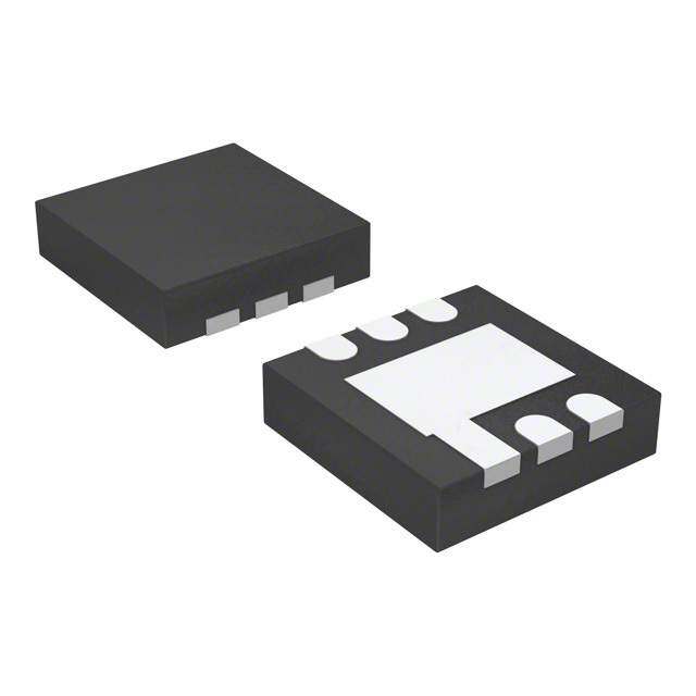
| 供应商器件封装 | 6-TDFN(2x2) |
| 其它名称 | AS1375-BTDT-25DKR |
| 包装 | Digi-Reel® |
| 安装类型 | 表面贴装 |
| 封装/外壳 | 6-UFDFN 裸露焊盘 |
| 工作温度 | -40°C ~ 85°C |
| 标准包装 | 1 |
| 电压-跌落(典型值) | 0.17V @ 200mA |
| 电压-输入 | 最高 5.5V |
| 电压-输出 | 2.5V |
| 电流-输出 | 200mA |
| 电流-限制(最小值) | - |
| 稳压器拓扑 | 正,固定式 |
| 稳压器数 | 1 |


- 商务部:美国ITC正式对集成电路等产品启动337调查
- 曝三星4nm工艺存在良率问题 高通将骁龙8 Gen1或转产台积电
- 太阳诱电将投资9.5亿元在常州建新厂生产MLCC 预计2023年完工
- 英特尔发布欧洲新工厂建设计划 深化IDM 2.0 战略
- 台积电先进制程称霸业界 有大客户加持明年业绩稳了
- 达到5530亿美元!SIA预计今年全球半导体销售额将创下新高
- 英特尔拟将自动驾驶子公司Mobileye上市 估值或超500亿美元
- 三星加码芯片和SET,合并消费电子和移动部门,撤换高东真等 CEO
- 三星电子宣布重大人事变动 还合并消费电子和移动部门
- 海关总署:前11个月进口集成电路产品价值2.52万亿元 增长14.8%


PDF Datasheet 数据手册内容提取
Datasheet AS1375 1µA Quiescent Current, 200mA LDO 1 General Description 2 Key Features The AS1375 low-power, positive voltage regulator is !"Input Voltage: 2V to 5.5V designed to deliver up to 200mA, while consuming only !"Low Dropout Voltage: 120mV @ 200mA load 1µA (typ.) of quiescent current. The device is available !"Output Voltage Range: 1.2V to 5.0V (50mV steps) in fixed output voltages between 1.2V and 5.0V (programmable in 50mV steps). The input voltage !"Max. Output Current: 200mA ranges from 2V to 5.5V. Operation with large input to !"Very Low Quiescent Current: 1µA output differential voltages is limited by the maximum !"Output Voltage Accuracy: ±1% power dissipation available from package and environment. !"Low Shutdown Current: 10nA (typ.) The very-low dropout voltage prolongs battery life and !"Integrated Overtemperature/Overcurrent Protection allows high current in small applications when operated !"Under-Voltage Lockout Feature with minimum input-to-output voltage differentials. The !"Enable Input device features very stable output voltage, strict output voltage regulation tolerances (±1%), and excellent line- !"Minimal External Components Required and load-regulation. !"Operating Temperature Range: -40°C to +85°C The device features integrated short-circuit and over !"6-pin TDFN 2x2mm Package current protection. Under-Voltage lockout prevents erratic operation when the input voltage is slowly decaying. Thermal Protection shuts down the device when die temperature reaches 160°C. This is a useful 3 Applications protection when the device is under sustained short circuit conditions. The device is perfectly suited for wireless handsets, The AS1375 is available in an 6-pin TDFN 2x2mm smartphones, PDAs, MP3 players, and other battery- package and is qualified for -40°C to +85°C operation. operated handheld devices, where the regulators have to be always on. Figure 1. AS1375 - Typical Application Diagram Input Output 2V to 5.5V 1.2V to 5V IN OUT 1CµIFN AS1375 C1µOFU T ON / OFF EN GND www.austriamicrosystems.com/LDOs/AS1375 Revision 1.02 1 - 10
AS1375 Datasheet - Pin Assignments 4 Pin Assignments Figure 2. Pin Assignments (Top View) IN 1 6 OUT GND 2 AS1375 5 GND EN 3 7 4 GND Pin Descriptions Table 1. Pin Descriptions Pin Name Pin Number Description IN 1 Input Supply Enable Input. A logic low disables the regulator. Connect to pin IN for EN 3 normal operation. GND 2, 4, 5 Ground Regulated Output Voltage. Current flowing out of this pin is equivalent DC OUT 6 load current. Ground. This pin also functions as a heat sink. Solder to a large pad or the Exposed Pad 7 circuit-board ground plane to maximize power dissipation. www.austriamicrosystems.com/LDOs/AS1375 Revision 1.02 2 - 10
AS1375 Datasheet - Absolute Maximum Ratings 5 Absolute Maximum Ratings Stresses beyond those listed in Table 2 may cause permanent damage to the device. These are stress ratings only, and functional operation of the device at these or any other conditions beyond those indicated in Section 6 Electrical Characteristics on page 4 is not implied. Exposure to absolute maximum rating conditions for extended periods may affect device reliability. Table 2. Absolute Maximum Ratings Parameter Min Max Units Notes Input Voltage +7 V Output Short-Circuit Duration Indefinite V Electrostatic Discharge 2 kV HBM MIL-Std. 883E 3015.7 methods Latch-Up 100 mA @85°C, JEDEC 78 Thermal Resistance !JA +140 ºC/W Junction Temperature +150 ºC Internally limited Operating Temperature Range -40 +85 ºC Storage Temperature Range -65 +150 ºC The reflow peak soldering temperature (body temperature) specified is in accordance with IPC/JEDEC J-STD- 020D “Moisture/Reflow Sensitivity Package Body Temperature +260 ºC Classification for Non-Hermetic Solid State Surface Mount Devices”. The lead finish for Pb-free leaded packages is matte tin (100% Sn). www.austriamicrosystems.com/LDOs/AS1375 Revision 1.02 3 - 10
AS1375 Datasheet - Electrical Characteristics 6 Electrical Characteristics VIN = VOUT + 500mV or VIN = +2V (whichever is greater),CIN = COUT = 1µF, EN = IN, TAMB = -40°C to +85ºC (unless otherwise specified). Typical values are at TAMB = +25ºC. Table 3. Electrical Characteristics Symbol Parameter Condition Min Typ Max Unit VIN Input Voltage 2 5.5 V IOUT = 10mA -1 +1 % Output Voltage Accuracy IOUT = 1 to 200mA, VOUT > 1.5V 1 -1.5 +1.5 % IOUT = 1 to 200mA, VOUT < 1.5V1 -2 +2 % VOUT Output Voltage Range 1.2 5.0 V Guaranteed Output Current IOUT 200 mA (RMS) ILIMIT Short-Circuit Current Limit VOUT = 0 250 330 450 mA In-Regulation Current Limit VOUT > 96% of nominal value 330 mA IOUT = 0 1.2 2 IQ Ground-Pin Current IOUT = 100µA 1 µA IOUT = 200mA 1.7 VVOINU T- Dropout Voltage2 IOUITO U=T 2 =0 02m00Am, A2V, V <O VUTO U"T 2 <.8 2V.8V 112700 230500 mV #VLNR Line Regulation VIN from (VOUT + 500mV) to 5.5V, -0.125 +0.125 %/V ILOAD = 10mA #VLDR Load Regulation IOUT = 1mA to 200mA 0.003 %/mA Shutdown IOFF Shutdown Supply Current EN = GND 10 100 nA VIH 2V < VIN < 5.5V 1.2 V EN Input Threshold VIL 2V < VIN < 5.5V 0.4 V IEN EN Input Bias Current EN = IN or GND 1 403 nA Startup Time from EN to 90% of VOUT(NOM) 750 µs Shutdown Time from EN to 10% of VOUT(NOM) 500 Thermal Protection Thermal Shutdown TSHDNN 160 ºC Temperature #TSHDNN Thermal Shutdown Hysteresis 20 ºC 1. Guaranteed by production test of load regulation. 2. Dropout voltage is defined as VIN - VOUT, when VOUT is 100mV below the value of VOUT measured for VIN = (VOUT(NOM) + 500mV). Since the minimum input voltage is 2V, this specification is only valid when VOUT(NOM) > 2V. 3. Guaranteed by design. Note: All limits are guaranteed. The parameters with min and max values are guaranteed with production tests or SQC (Statistical Quality Control) methods. www.austriamicrosystems.com/LDOs/AS1375 Revision 1.02 4 - 10
AS1375 Datasheet - Typical Operating Characteristics 7 Typical Operating Characteristics VIN = 3.5V, VOUT = 3.0V, TAMB = +25°C (unless otherwise specified). Figure 3. Line Regulation Figure 4. Load Regulation 3.05 3.05 V)3.025 V)3.025 e ( e ( g g a a olt 3 olt 3 V V ut ut p p ut ut O O 2.975 Iout = 0.1mA 2.975 Iout = 10mA Iout 0 100mA Iout = 200mA 2.95 2.95 3.5 3.75 4 4.25 4.5 4.75 5 5.25 5.5 0 25 50 75 100 125 150 175 200 Input Voltage (V) Output Current (mA) Figure 5. Ground Pin Current vs. Output Current Figure 6. Ground Pin Current vs. Input Voltage 2.5 2.5 Iout = 0.1mA Iout = 100mA 2.25 2.25 A) A) Iout = 200mA µ µ nt ( 2 nt ( 2 e e rr rr u u C C n 1.75 n 1.75 Pi Pi d d n 1.5 n 1.5 u u o o Gr Gr 1.25 1.25 1 1 0 25 50 75 100 125 150 175 200 3.5 3.75 4 4.25 4.5 4.75 5 5.25 5.5 Output Current (mA) Input Voltage (V) Figure 7. Output Voltage vs. Input Voltage - Dropout 3.06 3.04 V)3.02 e ( 3 g a olt2.98 V ut p2.96 ut O 2.94 2.92 Iload = 100mA Iload = 200mA 2.9 2.9 3 3.1 3.2 3.3 3.4 3.5 Input Voltage (V) www.austriamicrosystems.com/LDOs/AS1375 Revision 1.02 5 - 10
AS1375 Datasheet - Detailed Description 8 Detailed Description The AS1375 is an low-power and low-quiescent current linear-regulator specifically designed for space-limited applica- tions. These device can supply loads up to 200mA. As shown in Figure 8, the AS1375 consist of an integrated voltage reference, error amplifier, P-channel MOSFET pass transistor. Additional blocks include a current limiter, thermal sensor, and enable logic. Internal Voltage Reference The bandgap reference is connected to the error amplifier’s inverting input. The error amplifier compares this reference with the feedback voltage and amplifies the difference. If the feedback voltage is lower than the reference voltage, the pass-transistor gate is pulled low. This allows more current to pass to the output and increases the output voltage. If the feedback voltage is too high, the pass transistor gate is pulled high, allowing less current to pass to the output. Figure 8. AS1375 - Block Diagram IN Overcurrent Protection Voltage - Enable Con- EN and trol Logic Current Reference + OUT Thermal Protection AS1375 GND Current Limit The AS1375 include a current limiting circuitry to monitor and control the P-channel MOSFET pass transistor’s gate voltage, thus limiting the device output current to 300mA. Note: See Table 3 on page 4 for the min and max current limits. The output can be shorted to ground indefinitely without causing damage to the device. Thermal Protection Integrated thermal protection circuitry limits total power dissipation in the AS1375. When the junction temperature (TJ) exceeds +160ºC, the thermal sensor signals the shutdown logic, turning off the P-channel MOSFET pass transistor and allowing the device to cool down. The thermal sensor turns the pass transistor on again after the device’s junction temperature drops by 20ºC, resulting in a pulsed output during continuous thermal-overload conditions. Note: Thermal protection is designed to protect the devices in the event of fault conditions. For continuous operation, do not exceed the absolute maximum junction temperature rating of +150ºC. www.austriamicrosystems.com/LDOs/AS1375 Revision 1.02 6 - 10
AS1375 Datasheet - Application Information 9 Application Information Capacitor Selection and Regulator Stability For normal operation, use a 1µF capacitor at pin IN and a 1µF capacitor at pin OUT. Larger input capacitor values and lower ESR provide better noise rejection and line-transient response. Reduce output noise and improve load-transient response, stability, and power-supply rejection by using large output capacitors. Note: Some ceramic dielectrics exhibit large capacitance and ESR variation with temperature. With dielectrics such as Z5U and Y5V, it may be necessary to use a 2.2µF or larger output capacitor to ensure stability at tempera- tures below -10°C. With X7R or X5R dielectrics, 1µF is sufficient at all operating temperatures. Noise, PSRR, and Transient Response The AS1375 is designed to deliver low dropout and low quiescent currents in battery-powered systems. The power- supply rejection is 85dB at 1kHz and 50dB at 100kHz. When operating from sources other than batteries, improved supply-noise rejection and transient response can be achieved by increasing the values of the input and output capacitors, and through passive filtering techniques. Dropout Voltage The AS1375 minimum dropout voltage determines the lowest usable supply voltage. In battery-powered systems, this determines the useful end-of-life battery voltage. Since the AS1375 use a P-channel MOSFET pass transistor, the dropout voltage is a function of drain-to-source on- resistance (RDS(ON)) multiplied by ILOAD. www.austriamicrosystems.com/LDOs/AS1375 Revision 1.02 7 - 10
AS1375 Datasheet - Package Drawings and Markings 10 Package Drawings and Markings The device is available in a 6-pin TDFN 2x2mm package. Figure 9. 6-pin TDFN 2x2mm Package Diagram D2 Terminal Tip D e A INDEX AREA D/2 B (D/2 x E/2) L PIN#1 ID INDEX AREA D/2 x E/2 2 E/ E C a a a b EXPOSED PAD aaa C bbb C A B TOP VIEW BOTTOM VIEW ccc C 3 A B A SEATING PLANE 0.08 C 1 A SIDE VIEW Table 4. 4-bumps WL-CSP package Dimensions Symbol Min Typ Max Symbol Min Typ Max A 0.51 0.55 0.60 D BSC 1.95 2.00 2.05 A1 0.00 0.02 0.05 E BSC 1.95 2.00 2.05 A3 0.15 REF D2 1.30 1.45 1.55 b 0.20 0.25 0.32 E2 0.85 1.00 1.10 e 0.50 L 0.15 0.25 0.35 aaa 0.15 k 0.20 bbb 0.10 ND 3 ccc 0.10 N 6 Note: 1. All dimensions are in millimeters, angle is in degrees (°). 2. N is the total number of terminals. 3. The location of the terminal #1 identifier and terminal numbering convention conforms to JEDEC publication 95 SPP-002. 4. ND and NE refer to the number of terminals on each D and E side respectively. 5. NJR refer to non jedec registered. 6. Dimension b applies to metallized terminal and is measured between 0.15mm and 0.30mm from the terminal tip. If the terminal has the optional radius on the other end of the terminal, the dimension B should not be mea- sured in that radius area. 7. Coplanarity applies to the terminals and all other bottom surface metallization. www.austriamicrosystems.com/LDOs/AS1375 Revision 1.02 8 - 10
AS1375 Datasheet - Ordering Information 11 Ordering Information The devices are available as the standard products shown in Table 5. Table 5. Ordering Information Ordering Code Marking Output Description Delivery Form Package 1µA Quiescent Current, AS1375-BTDT-12 ABD 1.2V Tape and Reel 6-pin TDFN 2x2mm 200mA LDO 1µA Quiescent Current, AS1375-BTDT-18 ABE 1.8V Tape and Reel 6-pin TDFN 2x2mm 200mA LDO 1µA Quiescent Current, AS1375-BTDT-25 ABF 2.5V Tape and Reel 6-pin TDFN 2x2mm 200mA LDO 1µA Quiescent Current, AS1375-BTDT-30 ABG 3.0V Tape and Reel 6-pin TDFN 2x2mm 200mA LDO 1µA Quiescent Current, AS1375-BTDT-33 ABH 3.3V Tape and Reel 6-pin TDFN 2x2mm 200mA LDO Non-standard devices from 1.2V to 5.0V are available in 50mV steps. For more information and inquiries contact$ http://www.austriamicrosystems.com/contact Note: All products are RoHS compliant.$ Buy our products or get free samples online at ICdirect: http://www.austriamicrosystems.com/ICdirect$ $ Technical Support is found at http://www.austriamicrosystems.com/Technical-Support$ $ For further information and requests, please contact us mailto:sales@austriamicrosystems.com$ or find your local distributor at http://www.austriamicrosystems.com/distributor www.austriamicrosystems.com/LDOs/AS1375 Revision 1.02 9 - 10
AS1375 Datasheet Copyrights Copyright © 1997-2010, austriamicrosystems AG, Tobelbaderstrasse 30, 8141 Unterpremstaetten, Austria-Europe. Trademarks Registered ®. All rights reserved. The material herein may not be reproduced, adapted, merged, translated, stored, or used without the prior written consent of the copyright owner. All products and companies mentioned are trademarks or registered trademarks of their respective companies. Disclaimer Devices sold by austriamicrosystems AG are covered by the warranty and patent indemnification provisions appearing in its Term of Sale. austriamicrosystems AG makes no warranty, express, statutory, implied, or by description regarding the information set forth herein or regarding the freedom of the described devices from patent infringement. austriamicrosystems AG reserves the right to change specifications and prices at any time and without notice. Therefore, prior to designing this product into a system, it is necessary to check with austriamicrosystems AG for current information. This product is intended for use in normal commercial applications. Applications requiring extended temperature range, unusual environmental requirements, or high reliability applications, such as military, medical life-support or life-sustaining equipment are specifically not recommended without additional processing by austriamicrosystems AG for each application. For shipments of less than 100 parts the manufacturing flow might show deviations from the standard production flow, such as test flow or test location. The information furnished here by austriamicrosystems AG is believed to be correct and accurate. However, austriamicrosystems AG shall not be liable to recipient or any third party for any damages, including but not limited to personal injury, property damage, loss of profits, loss of use, interruption of business or indirect, special, incidental or consequential damages, of any kind, in connection with or arising out of the furnishing, performance or use of the technical data herein. No obligation or liability to recipient or any third party shall arise or flow out of austriamicrosystems AG rendering of technical or other services. $ Contact Information Headquarters austriamicrosystems AG$ Tobelbaderstrasse 30$ A-8141 Unterpremstaetten, Austria Tel: +43 (0) 3136 500 0$ Fax: +43 (0) 3136 525 01 For Sales Offices, Distributors and Representatives, please visit: http://www.austriamicrosystems.com/contact www.austriamicrosystems.com/LDOs/AS1375 Revision 1.02 10 - 10