ICGOO在线商城 > LD055C104KAB2A
 Datasheet下载
- 型号: LD055C104KAB2A
- 制造商: AVX
- 库位|库存: xxxx|xxxx
- 要求:
| 数量阶梯 | 香港交货 | 国内含税 |
| +xxxx | $xxxx | ¥xxxx |
查看当月历史价格
查看今年历史价格
LD055C104KAB2A产品简介:
ICGOO电子元器件商城为您提供LD055C104KAB2A由AVX设计生产,在icgoo商城现货销售,并且可以通过原厂、代理商等渠道进行代购。 提供LD055C104KAB2A价格参考以及AVXLD055C104KAB2A封装/规格参数等产品信息。 你可以下载LD055C104KAB2A参考资料、Datasheet数据手册功能说明书, 资料中有LD055C104KAB2A详细功能的应用电路图电压和使用方法及教程。
| 参数 | 数值 |
| 产品目录 | |
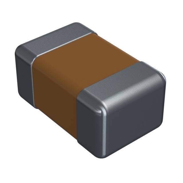
| 描述 | CAP CER 0.1UF 50V 10% X7R 0805多层陶瓷电容器MLCC - SMD/SMT 50volts 0.1uF 10% X7R |
| 产品分类 | |
| 品牌 | AVX Corporation |
| 产品手册 | |
| 产品图片 |
|
| rohs | 否含铅 / 不符合限制有害物质指令(RoHS)规范要求 |
| 产品系列 | MLCC,多层陶瓷电容器MLCC - SMD/SMT,AVX LD055C104KAB2ALD |
| 数据手册 | |
| 产品型号 | LD055C104KAB2A |
| 产品 | General Type MLCCs |
| 产品培训模块 | http://www.digikey.cn/PTM/IndividualPTM.page?site=cn&lang=zhs&ptm=21795 |
| 产品目录绘图 |
|
| 产品目录页面 | |
| 产品种类 | 多层陶瓷电容器MLCC - SMD/SMT |
| 其它名称 | 478-4931-1 |
| 包装 | 剪切带 (CT) |
| 厚度(最大值) | 0.037"(0.94mm) |
| 商标 | AVX |
| 外壳代码-in | 0805 |
| 外壳代码-mm | 2012 |
| 外壳宽度 | 1.25 mm |
| 外壳长度 | 2 mm |
| 外壳高度 | 0.94 mm |
| 大小/尺寸 | 0.079" 长 x 0.049" 宽(2.01mm x 1.25mm) |
| 安装类型 | 表面贴装,MLCC |
| 容差 | ±10% |
| 封装 | Reel |
| 封装/外壳 | 0805(2012 公制) |
| 封装/箱体 | 0805 (2012 metric) |
| 工作温度 | -55°C ~ 125°C |
| 工作温度范围 | - 55 C to + 125 C |
| 工厂包装数量 | 4000 |
| 应用 | 通用 |
| 引线形式 | - |
| 引线间距 | - |
| 最大工作温度 | + 125 C |
| 最小工作温度 | - 55 C |
| 标准包装 | 1 |
| 温度系数 | X7R |
| 温度系数/代码 | +/- 15 % |
| 特性 | - |
| 电介质 | X7R |
| 电压-额定 | 50V |
| 电压额定值 | 50 VDC |
| 电压额定值DC | 50 V |
| 电容 | 0.1µF |
| 端接类型 | SMD/SMT |
| 等级 | - |
| 类型 | MLCC Tin/Lead Termination |
| 系列 | LD05 |
| 高度-安装(最大值) | - |


- 商务部:美国ITC正式对集成电路等产品启动337调查
- 曝三星4nm工艺存在良率问题 高通将骁龙8 Gen1或转产台积电
- 太阳诱电将投资9.5亿元在常州建新厂生产MLCC 预计2023年完工
- 英特尔发布欧洲新工厂建设计划 深化IDM 2.0 战略
- 台积电先进制程称霸业界 有大客户加持明年业绩稳了
- 达到5530亿美元!SIA预计今年全球半导体销售额将创下新高
- 英特尔拟将自动驾驶子公司Mobileye上市 估值或超500亿美元
- 三星加码芯片和SET,合并消费电子和移动部门,撤换高东真等 CEO
- 三星电子宣布重大人事变动 还合并消费电子和移动部门
- 海关总署:前11个月进口集成电路产品价值2.52万亿元 增长14.8%


PDF Datasheet 数据手册内容提取
MLCC Tin/Lead Termination "B" (LD Series) C0G (NP0) – General Specifications AVX Corporation will support those customers for commercial and military Multilayer Ceramic Capacitors with a termination consisting of 5% minimum lead. This termination is indicated by the use of a “B” in the 12th position of the AVX Catalog Part Number. This fulfills AVX’s commitment to providing a full range of products to our customers. AVX has provided in the following pages a full range of values that we are currently offering in this special “B” termination. Please contact the factory if you require additional information on our MLCC Tin/Lead Termination “B” products. PART NUMBER (SEE PAGE 4 FOR COMPLETE PART NUMBER EXPLANATION) LD05 5 A 101 J A B 2 A Size Voltage Dielectric Capacitance Capacitance Failure Terminations Packaging Special LD02 - 0402 6.3V = 6 C0G (NP0) = A Code (In pF) Tolerance Rate B = 5% min lead 2 = 7" Reel Code LD03 - 0603 10V = Z X7R = C 2 Sig. Digits + B = ±.10 pF (<10pF) A = Not X = FLEXITERM® 4 = 13" Reel A = Std. LD04 - 0504* 16V = Y X5R = D Number of C = ±.25 pF (<10pF) Applicable with 5% min Product LD05 - 0805 Contact Factory 25V = 3 X8R = F Zeros D = ±.50 pF (<10pF) lead** LD06 - 1206 For LD10 - 1210 35V = D F = ±1% (≥ 10 pF) Multiples* LD12 - 1812 50V = 5 G = ±2% (≥ 10 pF) **X7R only LD13 - 1825 100V = 1 J = ±5% LD14 - 2225 200V = 2 K = ±10% LD20 - 2220 500V = 7 M = ±20% *LD04 has the same CV ranges as LD03. See FLEXITERM® section for CV options NOTE: Contact factory for availability of Tolerance Options for Specific Part Numbers. Contact factory for non-specified capacitance values. Insulation Resistance vs Temperature s)10,000 d a ar F m- h O 1,000 e ( c n a st esi 100 R n o ati ul s 0 In 0 20 40 60 80 100 Temperature °C The Important Information/Disclaimer is incorporated in these specifications by reference and should be reviewed in full before placing any order. 39 112916
MLCC Tin/Lead Termination “B” C0G (NP0) – Specifications and Test Methods Parameter/Test NP0 Specification Limits Measuring Conditions Operating Temperature Range -55ºC to +125ºC Temperature Cycle Chamber Capacitance Within specified tolerance Freq.: 1.0 MHz ± 10% for cap ≤ 1000 pF <30 pF: Q≥ 400+20 x Cap Value 1.0 kHz ± 10% for cap > 1000 pF Q ≥30 pF: Q≥ 1000 Voltage: 1.0Vrms ± .2V 100,000MΩ or 1000MΩ - μF, Charge device with rated voltage for Insulation Resistance whichever is less 60 ± 5 secs @ room temp/humidity Charge device with 250% of rated voltage for 1-5 seconds, w/charge and discharge current Dielectric Strength No breakdown or visual defects limited to 50 mA (max) Note: Charge device with 150% of rated voltage for 500V devices. Appearance No defects Deflection: 2mm Test Time: 30 seconds Capacitance Resistance to Variation ±5% or ±.5 pF, whichever is greater Flexure Stresses Q Meets Initial Values (As Above) Insulation ≥ Initial Value x 0.3 Resistance ≥ 95% of each terminal should be covered Dip device in eutectic solder at 230 ± 5ºC Solderability with fresh solder for 5.0 ± 0.5 seconds Appearance No defects, <25% leaching of either end terminal Capacitance ≤ ±2.5% or ±.25 pF, whichever is greater Variation Dip device in eutectic solder at 260ºC for 60 Resistance to Q Meets Initial Values (As Above) seconds. Store at room temperature for 24 ± 2 Solder Heat hours before measuring electrical properties. Insulation Meets Initial Values (As Above) Resistance Dielectric Meets Initial Values (As Above) Strength Appearance No visual defects Step 1: -55ºC ± 2º 30 ± 3 minutes Capacitance ≤ ±2.5% or ±.25 pF, whichever is greater Step 2: Room Temp ≤ 3 minutes Variation Q Meets Initial Values (As Above) Step 3: +125ºC ± 2º 30 ± 3 minutes Thermal Shock Insulation Meets Initial Values (As Above) Step 4: Room Temp ≤ 3 minutes Resistance Dielectric Repeat for 5 cycles and measure after Meets Initial Values (As Above) Strength 24 hours at room temperature Appearance No visual defects Capacitance ≤ ±3.0% or ± .3 pF, whichever is greater Variation Charge device with twice rated voltage in test chamber set at 125ºC ± 2ºC ≥ 30 pF: Q≥ 350 for 1000 hours (+48, -0). Q ≥10 pF, <30 pF: Q≥ 275 +5C/2 Load Life <10 pF: Q≥ 200 +10C Remove from test chamber and stabilize at room Insulation ≥ Initial Value x 0.3 (See Above) temperature for 24 hours Resistance before measuring. Dielectric Meets Initial Values (As Above) Strength Appearance No visual defects Capacitance ≤ ±5.0% or ± .5 pF, whichever is greater Variation Store in a test chamber set at 85ºC ± 2ºC/ 85% ± ≥ 30 pF: Q≥ 350 5% relative humidity for 1000 hours Load Q ≥10 pF, <30 pF: Q≥ 275 +5C/2 (+48, -0) with rated voltage applied. Humidity <10 pF: Q≥ 200 +10C Insulation Remove from chamber and stabilize at room ≥ Initial Value x 0.3 (See Above) Resistance temperature for 24 ± 2 hours before measuring. Dielectric Meets Initial Values (As Above) Strength The Important Information/Disclaimer is incorporated in these specifications 40 by reference and should be reviewed in full before placing any order. 112916
MLCC Tin/Lead Termination “B” C0G (NP0) – Capacitance Range PREFERRED SIZES ARE SHADED SIZE LD02 LD03 LD05 LD06 Soldering Reflow/Wave Reflow/Wave Reflow/Wave Reflow/Wave Packaging All Paper All Paper Paper/Embossed Paper/Embossed mm 1.00 ± 0.10 1.60 ± 0.15 2.01 ± 0.20 3.20 ± 0.20 (L) Length (in.) (0.040 ± 0.004) (0.063 ± 0.006) (0.079 ± 0.008) (0.126 ± 0.008) mm 0.50 ± 0.10 0.81 ± 0.15 1.25 ± 0.20 1.60 ± 0.20 W) Width (in.) (0.020 ± 0.004) (0.032 ± 0.006) (0.049 ± 0.008) (0.063 ± 0.008) mm 0.25 ± 0.15 0.35 ± 0.15 0.50 ± 0.25 0.50 ± 0.25 (t) Terminal (in.) (0.010 ± 0.006) (0.014 ± 0.006) (0.020 ± 0.010) (0.020 ± 0.010) WVDC 16 25 50 16 25 50 100 16 25 50 100 200 16 25 50 100 200 500 Cap 0.5 C C C G G G G J J J J J J J J J J J (pF) 1.0 C C C G G G G J J J J J J J J J J J 1.2 C C C G G G G J J J J J J J J J J J 1.5 C C C G G G G J J J J J J J J J J J 1.8 C C C G G G G J J J J J J J J J J J 2.2 C C C G G G G J J J J J J J J J J J 2.7 C C C G G G G J J J J J J J J J J J 3.3 C C C G G G G J J J J J J J J J J J 3.9 C C C G G G G J J J J J J J J J J J 4.7 C C C G G G G J J J J J J J J J J J 5.6 C C C G G G G J J J J J J J J J J J 6.8 C C C G G G G J J J J J J J J J J J 8.2 C C C G G G G J J J J J J J J J J J 10 C C C G G G G J J J J J J J J J J J 12 C C C G G G G J J J J J J J J J J J 15 C C C G G G G J J J J J J J J J J J 18 C C C G G G G J J J J J J J J J J J 22 C C C G G G G J J J J J J J J J J J 27 C C C G G G G J J J J J J J J J J J 33 C C C G G G G J J J J J J J J J J J 39 C C C G G G G J J J J J J J J J J J 47 C C C G G G G J J J J J J J J J J J 56 C C C G G G G J J J J J J J J J J J 68 C C C G G G G J J J J J J J J J J J 82 C C C G G G G J J J J J J J J J J J 100 C C C G G G G J J J J J J J J J J J 120 C C C G G G G J J J J J J J J J J J 150 C C C G G G G J J J J J J J J J J J 180 C C C G G G G J J J J J J J J J J J 220 C C C G G G G J J J J J J J J J J M 270 C C C G G G G J J J J M J J J J J M 330 C C C G G G G J J J J M J J J J J M 390 C C C G G G G J J J J M J J J J J M 470 C C C G G G J J J J M J J J J J M 560 G G G J J J J M J J J J J M 680 G G G J J J J J J J J J P 820 G G G J J J J J J J J M 1000 G G G J J J J J J J J Q 1200 G J J J J J J J Q 1500 J J J J J J M Q 1800 J J J J J M M 2200 J J N J J M P 2700 J J N J J M P 3300 J J J J M P 3900 J J J J M P 4700 J J J J M P 5600 J J M 6800 M M 8200 M M Cap 0.010 M M (pF) 0.012 0.015 0.018 0.022 0.027 0.033 0.039 0.047 0.068 0.082 0.1 WVDC 16 25 50 16 25 50 100 16 25 50 100 200 16 25 50 100 200 500 SIZE LD02 LD03 LD05 LD06 Letter A C E G J K M N P Q X Y Z Max. 0.33 0.56 0.71 0.90 0.94 1.02 1.27 1.40 1.52 1.78 2.29 2.54 2.79 Thickness (0.013) (0.022) (0.028) (0.035) (0.037) (0.040) (0.050) (0.055) (0.060) (0.070) (0.090) (0.100) (0.110) PAPER EMBOSSED The Important Information/Disclaimer is incorporated in these specifications by reference and should be reviewed in full before placing any order. 41 112916
MLCC Tin/Lead Termination “B” C0G (NP0) – Capacitance Range PREFERRED SIZES ARE SHADED SIZE LD10 LD12 LD13 LD14 Soldering Reflow Only Reflow Only Reflow Only Reflow Only Packaging Paper/Embossed All Embossed All Embossed All Embossed mm 3.20 + 0.20 4.50 ± 0.30 4.50 ± 0.30 5.72 ± 0.25 (L) Length (in.) (0.126 ± 0.008) (0.177 ± 0.012) (0.177 ± 0.012) (0.225 ± 0.010) mm 2.50 ± 0.20 3.20 ± 0.20 6.40 ± 0.40 6.35 ± 0.25 W) Width (in.) (0.098 ± 0.008) (0.126 ± 0.008) (0.252 ± 0.016) (0.250 ± 0.010) mm 0.50 ± 0.25 0.61 ± 0.36 0.61 ± 0.36 0.64 ± 0.39 (t) Terminal (in.) (0.020 ± 0.010) (0.024 ± 0.014) (0.024 ± 0.014) (0.025 ± 0.015) WVDC 25 50 100 200 500 25 50 100 200 500 50 100 200 50 100 200 Cap 0.5 (pF) 1.0 1.2 1.5 1.8 2.2 2.7 3.3 3.9 4.7 5.6 6.8 8.2 10 J 12 J 15 J 18 J 22 J 27 J 33 J 39 J 47 J 56 J 68 J 82 J 100 J 120 J 150 J 180 J 220 J 270 J 330 J 390 M 470 M 560 J J J J M 680 J J J J M 820 J J J J M 1000 J J J J M K K K K M M M M M M P 1200 J J J M M K K K K M M M M M M P 1500 J J J M M K K K K M M M M M M P 1800 J J J M K K K K M M M M M M P 2200 J J J Q K K K K P M M M M M P 2700 J J J Q K K K P Q M M M M M P 3300 J J J K K K P Q M M M M M P 3900 J J M K K K P Q M M M M M P 4700 J J M K K K P Q M M M M M P 5600 J J K K M P X M M M M M P 6800 J J K K M X M M M M M P 8200 J J K M M M M M M P Cap 0.010 J J K M M M M M M P (pF) 0.012 J J K M M M M M P 0.015 M M M M M M Y 0.018 M M P M M M Y 0.022 M M P M Y Y 0.027 M M P P Y Y 0.033 M M P P 0.039 M M P P 0.047 M M P P 0.068 M M P 0.082 M M Q 0.1 Q WVDC 25 50 100 200 500 25 50 100 200 500 50 100 200 50 100 200 SIZE LD10 LD12 LD13 LD14 Letter A C E G J K M N P Q X Y Z Max. 0.33 0.56 0.71 0.90 0.94 1.02 1.27 1.40 1.52 1.78 2.29 2.54 2.79 Thickness (0.013) (0.022) (0.028) (0.035) (0.037) (0.040) (0.050) (0.055) (0.060) (0.070) (0.090) (0.100) (0.110) PAPER EMBOSSED The Important Information/Disclaimer is incorporated in these specifications 42 by reference and should be reviewed in full before placing any order. 112916
MLCC Tin/Lead Termination “B” X8R – General Specifications AVX Corporation will support those customers for commercial and military Multilayer Ceramic Capacitors with a termination consisting of 5% minimum lead. This termination is indicated by the use of a “B” in the 12th position of the AVX Catalog Part Number. This fulfills AVX’s commitment to providing a full range of products to our customers. AVX has provided in the following pages a full range of values that we are currently offering in this special “B” termination. Please contact the factory if you require additional information on our MLCC Tin/Lead Termination “B” products. PART NUMBER (SEE PAGE 4 FOR COMPLETE PART NUMBER EXPLANATION) LD05 5 F 101 J A B 2 A Size Voltage Dielectric Capacitance Capacitance Failure Terminations Packaging Special LD02 - 0402 6.3V = 6 X8R = F Code (In pF) Tolerance Rate B = 5% min lead 2 = 7" Reel Code LD03 - 0603 10V = Z 2 Sig. Digits + B = ±.10 pF (<10pF) A = Not X = FLEXITERM® 4 = 13" Reel A = Std. LD04 - 0504* 16V = Y Number of C = ±.25 pF (<10pF) Applicable with 5% min Product LD05 - 0805 Contact Factory 25V = 3 Zeros D = ±.50 pF (<10pF) lead** LD06 - 1206 For LD10 - 1210 35V = D F = ±1% (≥ 10 pF) Multiples* LD12 - 1812 50V = 5 G = ±2% (≥ 10 pF) **X7R only LD13 - 1825 100V = 1 J = ±5% LD14 - 2225 200V = 2 K = ±10% LD20 - 2220 500V = 7 M = ±20% LD04 has the same CV ranges as LD03. See FLEXITERM® section for CV options NOTE: Contact factory for availability of Tolerance Options for Specific Part Numbers. Contact factory for non-specified capacitance values. The Important Information/Disclaimer is incorporated in these specifications by reference and should be reviewed in full before placing any order. 43 112916
MLCC Tin/Lead Termination “B” X8R – Specifications and Test Methods Parameter/Test X8R Specification Limits Measuring Conditions Operating Temperature Range -55ºC to +150ºC Temperature Cycle Chamber Capacitance Within specified tolerance Freq.: 1.0 kHz ± 10% ≤ 2.5% for ≥ 50V DC rating Dissipation Factor Voltage: 1.0Vrms ± .2V ≤ 3.5% for 25V DC and 16V DC rating 100,000MΩ or 1000MΩ - μF, Charge device with rated voltage for Insulation Resistance whichever is less 120 ± 5 secs @ room temp/humidity Charge device with 250% of rated voltage for 1-5 seconds, w/charge and discharge current Dielectric Strength No breakdown or visual defects limited to 50 mA (max) Note: Charge device with 150% of rated voltage for 500V devices. Appearance No defects Deflection: 2mm Capacitance Test Time: 30 seconds ≤ ±12% Resistance to Variation Flexure Dissipation Stresses Factor Meets Initial Values (As Above) Insulation ≥ Initial Value x 0.3 Resistance ≥ 95% of each terminal should be covered Dip device in eutectic solder at 230 ± 5ºC Solderability with fresh solder for 5.0 ± 0.5 seconds Appearance No defects, <25% leaching of either end terminal Capacitance ≤ ±7.5% Variation RSeoslidsetar nHceea tto DisFsaicptaotrion Meets Initial Values (As Above) sDecipo nddesv.ic Set oinre e autt ercotoicm s toelmdepre arat t2u6r0eº fCo rf o2r4 6 ±0 2 hours before measuring electrical properties. Insulation Meets Initial Values (As Above) Resistance Dielectric Meets Initial Values (As Above) Strength Appearance No visual defects Step 1: -55ºC ± 2º 30 ± 3 minutes Capacitance ≤ ±7.5% Step 2: Room Temp ≤ 3 minutes Variation Dissipation Meets Initial Values (As Above) Step 3: +125ºC ± 2º 30 ± 3 minutes Thermal Shock Factor Insulation Meets Initial Values (As Above) Step 4: Room Temp ≤ 3 minutes Resistance Dielectric Repeat for 5 cycles and measure after Meets Initial Values (As Above) Strength 24 ± 2 hours at room temperature Appearance No visual defects Capacitance Variation ≤ ±12.5% Charge device with 1.5 rated voltage (≤ 10V) in test chamber set at 150ºC ± 2ºC Dissipation ≤ Initial Value x 2.0 (See Above) for 1000 hours (+48, -0) Load Life Factor Insulation ≥ Initial Value x 0.3 (See Above) Remove from test chamber and stabilize at room Resistance temperature for 24 ± 2 hours before measuring. Dielectric Meets Initial Values (As Above) Strength Appearance No visual defects Capacitance ≤ ±12.5% Store in a test chamber set at 85ºC ± 2ºC/ 85% ± Variation 5% relative humidity for 1000 hours Load DisFsaicptaotrion ≤ Initial Value x 2.0 (See Above) (+48, -0) with rated voltage applied. Humidity Insulation Remove from chamber and stabilize at room ≥ Initial Value x 0.3 (See Above) Resistance temperature and humidity for 24 ± 2 hours before measuring. Dielectric Meets Initial Values (As Above) Strength The Important Information/Disclaimer is incorporated in these specifications 44 by reference and should be reviewed in full before placing any order. 112916
MLCC Tin/Lead Termination “B” X8R – Capacitance Range SIZE LD03 LD05 LD06 WVDC 25V 50V 25V 50V 25V 50V 271 Cap 270 G G 331 (pF) 330 G G J J 471 470 G G J J 681 680 G G J J 102 1000 G G J J J J 152 1500 G G J J J J 182 1800 G G J J J J 222 2200 G G J J J J 272 2700 G G J J J J 332 3300 G G J J J J 392 3900 G G J J J J 472 4700 G G J J J J 562 5600 G G J J J J 682 6800 G G J J J J 822 Cap 8200 G G J J J J 103 (μF) 0.01 G G J J J J 123 0.012 G G J J J J 153 0.015 G G J J J J 183 0.018 G G J J J J 223 0.022 G G J J J J 273 0.027 G G J J J J 333 0.033 G G J J J J 393 0.039 G G J J J J 473 0.047 G G J J J J 563 0.056 G N N M M 683 0.068 G N N M M 823 0.082 N N M M 104 0.1 N N M M 124 0.12 N N M M 154 0.15 N N M M 184 0.18 N M M 224 0.22 N M M 274 0.27 M M 334 0.33 M M 394 0.39 M 474 0.47 M 684 0.68 824 0.82 105 1 WVDC 25V 50V 25V 50V 25V 50V SIZE LD03 LD05 LD06 Letter A C E G J K M N P Q X Y Z Max. 0.33 0.56 0.71 0.90 0.94 1.02 1.27 1.40 1.52 1.78 2.29 2.54 2.79 Thickness (0.013) (0.022) (0.028) (0.035) (0.037) (0.040) (0.050) (0.055) (0.060) (0.070) (0.090) (0.100) (0.110) PAPER EMBOSSED The Important Information/Disclaimer is incorporated in these specifications by reference and should be reviewed in full before placing any order. 45 112916
MLCC Tin/Lead Termination “B” X7R –General Specifications AVX Corporation will support those customers for commercial and military Multilayer Ceramic Capacitors with a termination consisting of 5% minimum lead. This termination is indicated by the use of a “B” in the 12th position of the AVX Catalog Part Number. This fulfills AVX’s commitment to providing a full range of products to our customers. AVX has provided in the following pages a full range of values that we are currently offering in this special “B” termination. Please contact the factory if you require additional information on our MLCC Tin/Lead Termination “B” products. PART NUMBER (SEE PAGE 4 FOR COMPLETE PART NUMBER EXPLANATION) LD05 5 C 101 J A B 2 A Size Voltage Dielectric Capacitance Capacitance Failure Terminations Packaging Special LD03 - 0603 6.3V = 6 X7R = C Code (In pF) Tolerance Rate B = 5% min lead 2 = 7" Reel Code LD04 - 0504* 10V = Z 2 Sig. Digits + B = ±.10 pF (<10pF) A = Not X = FLEXITERM® 4 = 13" Reel A = Std. LD05 - 0805 16V = Y Number of C = ±.25 pF (<10pF) Applicable with 5% min Product Contact Factory LD06 - 1206 25V = 3 Zeros D = ±.50 pF (<10pF) lead** For LD10 - 1210 35V = D F = ±1% (≥ 10 pF) Multiples* LD12 - 1812 50V = 5 G = ±2% (≥ 10 pF) **X7R only LD13 - 1825 100V = 1 J = ±5% LD14 - 2225 200V = 2 K = ±10% LD20 - 2220 500V = 7 M = ±20% *LD04 has the same CV ranges as LD03. See FLEXITERM® section for CV options NOTE: Contact factory for availability of Tolerance Options for Specific Part Numbers. Contact factory for non-specified capacitance values. The Important Information/Disclaimer is incorporated in these specifications 46 by reference and should be reviewed in full before placing any order. 112916
MLCC Tin/Lead Termination “B” X7R –Specifications and Test Methods Parameter/Test X7R Specification Limits Measuring Conditions Operating Temperature Range -55ºC to +125ºC Temperature Cycle Chamber Capacitance Within specified tolerance ≤ 10% for ≥ 50V DC rating Freq.: 1.0 kHz ± 10% ≤ 12.5% for 25V DC rating Dissipation Factor Voltage: 1.0Vrms ± .2V ≤ 12.5% for 25V and 16V DC rating ≤ 12.5% for ≤ 10V DC rating 100,000MΩ or 1000MΩ - μF, Charge device with rated voltage for Insulation Resistance whichever is less 120 ± 5 secs @ room temp/humidity Charge device with 250% of rated voltage for 1-5 seconds, w/charge and discharge current Dielectric Strength No breakdown or visual defects limited to 50 mA (max) Note: Charge device with 150% of rated voltage for 500V devices. Appearance No defects Deflection: 2mm Capacitance Test Time: 30 seconds ≤ ±12% Resistance to Variation Flexure Dissipation Stresses Factor Meets Initial Values (As Above) Insulation ≥ Initial Value x 0.3 Resistance ≥ 95% of each terminal should be covered Dip device in eutectic solder at 230 ± 5ºC Solderability with fresh solder for 5.0 ± 0.5 seconds Appearance No defects, <25% leaching of either end terminal Capacitance ≤ ±7.5% Variation Dissipation Dip device in eutectic solder at 260ºC for 60 Resistance to Meets Initial Values (As Above) Factor seconds. Store at room temperature for 24 ± 2 Solder Heat Insulation hours before measuring electrical properties. Meets Initial Values (As Above) Resistance Dielectric Meets Initial Values (As Above) Strength Appearance No visual defects Step 1: -55ºC ± 2º 30 ± 3 minutes Capacitance ≤ ±7.5% Step 2: Room Temp ≤ 3 minutes Variation Dissipation Meets Initial Values (As Above) Step 3: +125ºC ± 2º 30 ± 3 minutes Thermal Shock Factor Insulation Meets Initial Values (As Above) Step 4: Room Temp ≤ 3 minutes Resistance Dielectric Repeat for 5 cycles and measure after Meets Initial Values (As Above) Strength 24 ± 2 hours at room temperature Appearance No visual defects Capacitance Variation ≤ ±12.5% Charge device with 1.5 rated voltage (≤ 10V) in test chamber set at 125ºC ± 2ºC Dissipation ≤ Initial Value x 2.0 (See Above) for 1000 hours (+48, -0) Load Life Factor Insulation ≥ Initial Value x 0.3 (See Above) Remove from test chamber and stabilize at room Resistance temperature for 24 ± 2 hours before measuring. Dielectric Meets Initial Values (As Above) Strength Appearance No visual defects Capacitance ≤ ±12.5% Store in a test chamber set at 85ºC ± 2ºC/ 85% ± Variation 5% relative humidity for 1000 hours Load DisFsaicptaotrion ≤ Initial Value x 2.0 (See Above) (+48, -0) with rated voltage applied. Humidity Insulation Remove from chamber and stabilize at room ≥ Initial Value x 0.3 (See Above) Resistance temperature and humidity for 24 ± 2 hours before measuring. Dielectric Meets Initial Values (As Above) Strength The Important Information/Disclaimer is incorporated in these specifications by reference and should be reviewed in full before placing any order. 47 112916
MLCC Tin/Lead Termination “B” X7R –Capacitance Range PREFERRED SIZES ARE SHADED SIZE LD02 LD03 LD05 LD06 Soldering Reflow/Wave Reflow/Wave Reflow/Wave Reflow/Wave Packaging All Paper All Paper Paper/Embossed Paper/Embossed mm 1.00 ± 0.10 1.60 ± 0.15 2.01 ± 0.20 3.20 ± 0.20 (L) Length (in.) (0.040 ± 0.004) (0.063 ± 0.006) (0.079 ± 0.008) (0.126 ± 0.008) mm 0.50 ± 0.10 0.81 ± 0.15 1.25 ± 0.20 1.60 ± 0.20 W) Width (in.) (0.020 ± 0.004) (0.032 ± 0.006) (0.049 ± 0.008) (0.063 ± 0.008) mm 0.25 ± 0.15 0.35 ± 0.15 0.50 ± 0.25 0.50 ± 0.25 (t) Terminal (in.) (0.010 ± 0.006) (0.014 ± 0.006) (0.020 ± 0.010) (0.020 ± 0.010) WVDC 16 25 50 6.3 10 16 25 50 100 200 6.3 10 16 25 50 100 200 6.3 10 16 25 50 100 200 500 Cap 100 (pF) 150 220 C 330 C G G G J J J J J J K 470 C G G G J J J J J J K 680 C G G G J J J J J J K 1000 C G G G J J J J J J K 1500 C G G J J J J J J J J J J J J M 2200 C G G J J J J J J J J J J J J M 3300 C C G G J J J J J J J J J J J J M 4700 C C G G J J J J J J J J J J J J M 6800 C C G G J J J J J J J J J J J J P Cap 0.010 C C G G J J J J J J J J J J J J P (μF) 0.015 C G G J J J J J J J J J J J M 0.022 C G G J J J J J N J J J J J M 0.033 C G G J J J J N J J J J J M 0.047 G G G J J J J N J J J J J M 0.068 G G G J J J J N J J J J J P 0.10 C* G G G G J J J J N J J J J P P 0.15 G G J J J N N J J J J Q 0.22 G G J J N N N J J J J Q 0.33 N N N N N J J M P Q 0.47 J* N N N N N M M M P Q 0.68 N N N M M Q Q Q 1.0 J* J* N N N* M M Q Q Q 1.5 P Q Q 2.2 J* P* Q Q Q 3.3 4.7 P* P* Q* Q* Q* 10 P* P Q* Q* Q 22 Q* 47 100 WVDC 16 25 50 6.3 10 16 25 50 100 200 6.3 10 16 25 50 100 200 6.3 10 16 25 50 100 200 500 SIZE LD02 LD03 LD05 LD06 Letter A C E G J K M N P Q X Y Z Max. 0.33 0.56 0.71 0.90 0.94 1.02 1.27 1.40 1.52 1.78 2.29 2.54 2.79 Thickness (0.013) (0.022) (0.028) (0.035) (0.037) (0.040) (0.050) (0.055) (0.060) (0.070) (0.090) (0.100) (0.110) PAPER EMBOSSED = Under Development The Important Information/Disclaimer is incorporated in these specifications 48 by reference and should be reviewed in full before placing any order. 112916
MLCC Tin/Lead Termination “B” X7R – Capacitance Range PREFERRED SIZES ARE SHADED SIZE LD10 LD12 LD13 LD20 LD14 Soldering Reflow Only Reflow Only Reflow Only Reflow Only Reflow Only Packaging Paper/Embossed All Embossed All Embossed All Embossed All Embossed mm 3.20 + 0.20 4.50 ± 0.30 4.50 ± 0.30 5.70 ± 0.50 5.72 ± 0.25 (L) Length (in.) (0.126 ± 0.008) (0.177 ± 0.012) (0.177 ± 0.012) (0.224 ± 0.020) (0.225 ± 0.010) mm 2.50 ± 0.20 3.20 ± 0.20 6.40 ± 0.40 5.00 ± 0.40 6.35 ± 0.25 W) Width (in.) (0.098 ± 0.008) (0.126 ± 0.008) (0.252 ± 0.016) (0.197 ± 0.016) (0.250 ± 0.010) mm 0.50 ± 0.25 0.61 ± 0.36 0.61 ± 0.36 0.64 ± 0.39 0.64 ± 0.39 (t) Terminal (in.) (0.020 ± 0.010) (0.024 ± 0.014) (0.024 ± 0.014) (0.025 ± 0.015) (0.025 ± 0.015) WVDC 10 16 25 50 100 200 500 50 100 200 500 50 100 25 50 100 200 50 100 Cap 100 (pF) 150 220 330 470 680 1000 1500 J J J J J J M 2200 J J J J J J M 3300 J J J J J J M 4700 J J J J J J M 6800 J J J J J J M Cap 0.010 J J J J J J M K K K K M M X X X M P (μF) 0.015 J J J J J J P K K K P M M X X X M P 0.022 J J J J J J Q K K K P M M X X X M P 0.033 J J J J J J Q K K K X M M X X X M P 0.047 J J J J J J K K K Z M M X X X M P 0.068 J J J J J M K K K Z M M X X X M P 0.10 J J J J J M K K K Z M M X X X M P 0.15 J J J J M Z K K P M M X X X M P 0.22 J J J J P Z K K P M M X X X M P 0.33 J J J J Q K M X M M X X X M P 0.47 M M M M Q K P M M X X X M P 0.68 M M P X X M Q M P X X M P 1.0 N N P X Z M X M P X X M P 1.5 N N Z Z Z Z Z M X X M X 2.2 X X Z Z Z Z Z X X M 3.3 X X Z Z Z X Z 4.7 X X Z Z Z X Z 10 Z Z Z Z Z Z 22 Z Z Z 47 100 WVDC 10 16 25 50 100 200 500 50 100 200 500 50 100 25 50 100 200 50 100 SIZE LD10 LD12 LD13 LD20 LD14 Letter A C E G J K M N P Q X Y Z Max. 0.33 0.56 0.71 0.90 0.94 1.02 1.27 1.40 1.52 1.78 2.29 2.54 2.79 Thickness (0.013) (0.022) (0.028) (0.035) (0.037) (0.040) (0.050) (0.055) (0.060) (0.070) (0.090) (0.100) (0.110) PAPER EMBOSSED The Important Information/Disclaimer is incorporated in these specifications by reference and should be reviewed in full before placing any order. 49 011320
MLCC Tin/Lead Termination “B” X5R – General Specifications AVX Corporation will support those customers for commercial and military Multilayer Ceramic Capacitors with a termination consisting of 5% minimum lead. This termination is indicated by the use of a “B” in the 12th position of the AVX Catalog Part Number. This fulfills AVX’s commitment to providing a full range of products to our customers. AVX has provided in the following pages a full range of values that we are currently offering in this special “B” termination. Please contact the factory if you require additional information on our MLCC Tin/Lead Termination “B” products. PART NUMBER (SEE PAGE 4 FOR COMPLETE PART NUMBER EXPLANATION) LD05 5 D 101 J A B 2 A Size Voltage Dielectric Capacitance Capacitance Failure Terminations Packaging Special LD02 - 0402 6.3V = 6 X5R = D Code (In pF) Tolerance Rate B = 5% min lead 2 = 7" Reel Code LD03 - 0603 10V = Z 2 Sig. Digits + B = ±.10 pF (<10pF) A = Not X = FLEXITERM® 4 = 13" Reel A = Std. LD04 - 0504* 16V = Y Number of C = ±.25 pF (<10pF) Applicable with 5% min Product LD05 - 0805 Contact Factory 25V = 3 Zeros D = ±.50 pF (<10pF) lead** LD06 - 1206 For LD10 - 1210 35V = D F = ±1% (≥ 10 pF) Multiples* LD12 - 1812 50V = 5 G = ±2% (≥ 10 pF) **X7R only LD13 - 1825 100V = 1 J = ±5% LD14 - 2225 200V = 2 K = ±10% LD20 - 2220 500V = 7 M = ±20% *LD04 has the same CV ranges as LD03. See FLEXITERM® section for CV options NOTE: Contact factory for availability of Tolerance Options for Specific Part Numbers. Contact factory for non-specified capacitance values. TYPICAL ELECTRICAL CHARACTERISTICS Temperature Coefficient Insulation Resistance vs Temperature 20 ds)10,000 a 15 ar F - 10 m e acitanc 50 nce (Oh 1,000 p a Ca -5 esist 100 % -10 n R -15 atio -20 ul -60 -40 -20 0 +20 +40 +60 +80 ns 00 20 40 60 80 100 120 I Temperature °C Temperature °C The Important Information/Disclaimer is incorporated in these specifications 50 by reference and should be reviewed in full before placing any order. 112916
MLCC Tin/Lead Termination “B” X5R – Specifications and Test Methods Parameter/Test X5R Specification Limits Measuring Conditions Operating Temperature Range -55ºC to +85ºC Temperature Cycle Chamber Capacitance Within specified tolerance ≤ 2.5% for ≥ 50V DC rating Freq.: 1.0 kHz ± 10% ≤ 3.0% for 25V, 35V DC rating Voltage: 1.0Vrms ± .2V Dissipation Factor ≤ 12.5% Max. for 16V DC rating and lower Contact For Cap > 10 μF, 0.5Vrms @ 120Hz Factory for DF by PN 10,000MΩ or 500MΩ - μF, Charge device with rated voltage for Insulation Resistance whichever is less 120 ± 5 secs @ room temp/humidity Charge device with 250% of rated voltage for Dielectric Strength No breakdown or visual defects 1-5 seconds, w/charge and discharge current limited to 50 mA (max) Appearance No defects Deflection: 2mm Capacitance Test Time: 30 seconds ≤ ±12% Resistance to Variation Flexure Dissipation Stresses Factor Meets Initial Values (As Above) Insulation ≥ Initial Value x 0.3 Resistance ≥ 95% of each terminal should be covered Dip device in eutectic solder at 230 ± 5ºC Solderability with fresh solder for 5.0 ± 0.5 seconds Appearance No defects, <25% leaching of either end terminal Capacitance ≤ ±7.5% Variation Dissipation Dip device in eutectic solder at 260ºC for 60 Resistance to Meets Initial Values (As Above) Factor seconds. Store at room temperature for 24 ± 2 Solder Heat Insulation hours before measuring electrical properties. Meets Initial Values (As Above) Resistance Dielectric Meets Initial Values (As Above) Strength Appearance No visual defects Step 1: -55ºC ± 2º 30 ± 3 minutes Capacitance ≤ ±7.5% Step 2: Room Temp ≤ 3 minutes Variation Dissipation Meets Initial Values (As Above) Step 3: +85ºC ± 2º 30 ± 3 minutes Thermal Shock Factor Insulation Meets Initial Values (As Above) Step 4: Room Temp ≤ 3 minutes Resistance Dielectric Repeat for 5 cycles and measure after Meets Initial Values (As Above) Strength 24 ± 2 hours at room temperature Appearance No visual defects Capacitance Charge device with 1.5X rated voltage in test Variation ≤ ±12.5% chamber set at 85ºC ± 2ºC for 1000 hours (+48, -0). Note: Contact factory for *optional Dissipation ≤ Initial Value x 2.0 (See Above) specification part numbers that are tested at Load Life Factor < 1.5X rated voltage. Insulation ≥ Initial Value x 0.3 (See Above) Resistance Remove from test chamber and stabilize at room Dielectric temperature for 24 ± 2 hours before measuring. Meets Initial Values (As Above) Strength Appearance No visual defects Capacitance ≤ ±12.5% Store in a test chamber set at 85ºC ± 2ºC/ 85% ± Variation 5% relative humidity for 1000 hours Load DisFsaicptaotrion ≤ Initial Value x 2.0 (See Above) (+48, -0) with rated voltage applied. Humidity Insulation Remove from chamber and stabilize at room ≥ Initial Value x 0.3 (See Above) Resistance temperature and humidity for 24 ± 2 hours before measuring. Dielectric Meets Initial Values (As Above) Strength The Important Information/Disclaimer is incorporated in these specifications by reference and should be reviewed in full before placing any order. 51 112916
MLCC Tin/Lead Termination “B” X5R – Capacitance Range PREFERRED SIZES ARE SHADED SIZE LD02 LD03 LD05 LD06 LD10 LD12 Soldering Reflow/Wave Reflow/Wave Reflow/Wave Reflow/Wave Reflow/Wave Packaging All Paper All Paper Paper/Embossed Paper/Embossed Paper/Embossed mm 1.00 ± 0.10 1.60 ± 0.15 2.01 ± 0.20 3.20 ± 0.20 3.20 ± 0.20 (L) Length (in.) (0.040 ± 0.004) (0.063 ± 0.006) (0.079 ± 0.008) (0.126 ± 0.008) (0.126 ± 0.008) mm 0.50 ± 0.10 0.81 ± 0.15 1.25 ± 0.20 1.60 ± 0.20 2.50 ± 0.20 W) Width (in.) (0.020 ± 0.004) (0.032 ± 0.006) (0.049 ± 0.008) (0.063 ± 0.008) (0.098 ± 0.008) mm 0.25 ± 0.15 0.35 ± 0.15 0.50 ± 0.25 0.50 ± 0.25 0.50 ± 0.25 (t) Terminal (in.) (0.010 ± 0.006) (0.014 ± 0.006) (0.020 ± 0.010) (0.020 ± 0.010) (0.020 ± 0.010) WVDC 4 6.3 10 16 25 50 4 6.3 10 16 25 35 50 6.3 10 16 25 35 506.3 10 16 25 35 50 4 6.3 10 16 25 35 50 6.3 10 25 50 Cap 100 (pF) 150 220 C 330 C 470 C 680 C 1000 C 1500 C 2200 C 3300 C 4700 C G 6800 C G Cap 0.010 C G (μF) 0.015 C G G G 0.022 C C G G G N 0.033 C G G G N 0.047 C C G G G N 0.068 C G G N 0.10 C C C G G N N 0.15 G N N 0.22 C* G G N N Q 0.33 G G N 0.47 C* C* G N Q Q X 0.68 G N 1.0 C* C* C* G G G J* N N P* Q Q X X X 1.5 2.2 C* G* G* J* J* N N N Q Q Z X 3.3 J* J* J* J* N N X X 4.7 J* J* J* N N N* N* X X X X Q Z 10 K* P P P X X X X X Z Z Z 22 P* X X X X Z Z Z Z 47 X Z* 100 Z* Z WVDC 4 6.3 10 16 25 50 4 6.3 10 16 25 35 50 6.3 10 16 25 35 506.3 10 16 25 35 50 4 6.3 10 16 25 35 50 6.3 10 25 50 SIZE LD02 LD03 LD05 LD06 LD10 LD12 Letter A C E G J K M N P Q X Y Z Max. 0.33 0.56 0.71 0.90 0.94 1.02 1.27 1.40 1.52 1.78 2.29 2.54 2.79 Thickness (0.013) (0.022) (0.028) (0.035) (0.037) (0.040) (0.050) (0.055) (0.060) (0.070) (0.090) (0.100) (0.110) PAPER EMBOSSED *Optional Specifications – Contact factory NOTE: Contact factory for non-specified capacitance values The Important Information/Disclaimer is incorporated in these specifications 52 by reference and should be reviewed in full before placing any order. 112916