ICGOO在线商城 > ISO1I811T

 Datasheet下载
- 型号: ISO1I811T
- 制造商: Infineon
- 库位|库存: xxxx|xxxx
- 要求:
| 数量阶梯 | 香港交货 | 国内含税 |
| +xxxx | $xxxx | ¥xxxx |
查看当月历史价格
查看今年历史价格
ISO1I811T产品简介:
ICGOO电子元器件商城为您提供ISO1I811T由Infineon设计生产,在icgoo商城现货销售,并且可以通过原厂、代理商等渠道进行代购。 提供ISO1I811T价格参考以及InfineonISO1I811T封装/规格参数等产品信息。 你可以下载ISO1I811T参考资料、Datasheet数据手册功能说明书, 资料中有ISO1I811T详细功能的应用电路图电压和使用方法及教程。
| 参数 | 数值 |
| 产品目录 | |
| ChannelType | 单向 |
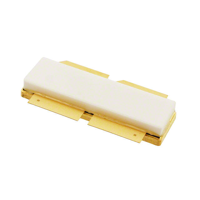
| 描述 | IC DGTL ISO 8CH PAR SER 48TSSOP |
| 产品分类 | |
| IsolatedPower | 无 |
| 品牌 | Infineon Technologies |
| 数据手册 | http://www.infineon.com/dgdl/Preliminary_Datasheet_ISO1I811T_V1_0.pdf?folderId=db3a30431b3e89eb011b8dbc543010a5&fileId=db3a30432ea425a4012ed83864253845 |
| 产品图片 |
|
| 产品型号 | ISO1I811T |
| PulseWidthDistortion(Max) | - |
| rohs | 无铅 / 符合限制有害物质指令(RoHS)规范要求 |
| 产品系列 | ISOFACE™ |
| 上升/下降时间(典型值) | - |
| 传播延迟tpLH/tpHL(最大值) | - |
| 供应商器件封装 | 48-TSSOP |
| 共模瞬态抗扰度(最小值) | 25kV/µs |
| 其它名称 | ISO1I811TCT |
| 包装 | 剪切带 (CT) |
| 封装/外壳 | 48-TFSOP(0.240",6.10mm 宽) |
| 工作温度 | -40°C ~ 85°C |
| 技术 | 磁耦合 |
| 数据速率 | - |
| 标准包装 | 1 |
| 电压-电源 | 2.85 V ~ 5.5 V |
| 电压-隔离 | 500VAC |
| 类型 | I²C, SPI |
| 脉宽失真(最大) | - |
| 输入-输入侧1/输入侧2 | 8/0 |
| 通道数 | 8 |
| 通道类型 | 单向 |
| 配用 | /product-detail/zh/EVALISO1I811TTOBO1/EVALISO1I811TTOBO1-ND/4862949 |
| 隔离式电源 | 无 |


- 商务部:美国ITC正式对集成电路等产品启动337调查
- 曝三星4nm工艺存在良率问题 高通将骁龙8 Gen1或转产台积电
- 太阳诱电将投资9.5亿元在常州建新厂生产MLCC 预计2023年完工
- 英特尔发布欧洲新工厂建设计划 深化IDM 2.0 战略
- 台积电先进制程称霸业界 有大客户加持明年业绩稳了
- 达到5530亿美元!SIA预计今年全球半导体销售额将创下新高
- 英特尔拟将自动驾驶子公司Mobileye上市 估值或超500亿美元
- 三星加码芯片和SET,合并消费电子和移动部门,撤换高东真等 CEO
- 三星电子宣布重大人事变动 还合并消费电子和移动部门
- 海关总署:前11个月进口集成电路产品价值2.52万亿元 增长14.8%


PDF Datasheet 数据手册内容提取
ISOFACE™ ISO1I811T Isolated 8 Channel Digital Input with IEC61131-2 Type 1/2/3 Characteristics Data Sheet Revision 2.0, 2012-06-14 Industrial & Multimarket
Edition 2012-06-14 Published by Infineon Technologies AG 81726 Munich, Germany © 2012 Infineon Technologies AG All Rights Reserved. Legal Disclaimer The information given in this document shall in no event be regarded as a guarantee of conditions or characteristics. With respect to any examples or hints given herein, any typical values stated herein and/or any information regarding the application of the device, Infineon Technologies hereby disclaims any and all warranties and liabilities of any kind, including without limitation, warranties of non-infringement of intellectual property rights of any third party. Information For further information on technology, delivery terms and conditions and prices, please contact the nearest Infineon Technologies Office (www.infineon.com). Warnings Due to technical requirements, components may contain dangerous substances. For information on the types in question, please contact the nearest Infineon Technologies Office. Infineon Technologies components may be used in life-support devices or systems only with the express written approval of Infineon Technologies, if a failure of such components can reasonably be expected to cause the failure of that life-support device or system or to affect the safety or effectiveness of that device or system. Life support devices or systems are intended to be implanted in the human body or to support and/or maintain and sustain and/or protect human life. If they fail, it is reasonable to assume that the health of the user or other persons may be endangered.
ISO1I811T ISO1I811T Revision History: 2012-06-14, Revision 2.0 Previous Version: Preliminary Data Sheet V1.0 Page Subjects (major changes since last revision) V2.0 Data Sheet Page25 Parallel Interface timing table updated Page26 Serial Interface timing table updated Data Sheet 3 Revision 2.0, 2012-06-14
ISO1I811T 1 Pin Configuration and Functionality . . . . . . . . . . . . . . . . . . . . . . . . . . . . . . . . . . . . . . . . . . . . . . . . . 6 1.1 Pin Configuration . . . . . . . . . . . . . . . . . . . . . . . . . . . . . . . . . . . . . . . . . . . . . . . . . . . . . . . . . . . . . . . . . 6 1.2 Pin Functionality . . . . . . . . . . . . . . . . . . . . . . . . . . . . . . . . . . . . . . . . . . . . . . . . . . . . . . . . . . . . . . . . . . 8 1.2.1 Pins of Sensor Interface . . . . . . . . . . . . . . . . . . . . . . . . . . . . . . . . . . . . . . . . . . . . . . . . . . . . . . . . . . 8 1.2.2 Pins of Serial and Parallel logic Interface . . . . . . . . . . . . . . . . . . . . . . . . . . . . . . . . . . . . . . . . . . . . . 9 2 Blockdiagram . . . . . . . . . . . . . . . . . . . . . . . . . . . . . . . . . . . . . . . . . . . . . . . . . . . . . . . . . . . . . . . . . . 10 3 Functional Description . . . . . . . . . . . . . . . . . . . . . . . . . . . . . . . . . . . . . . . . . . . . . . . . . . . . . . . . . . . 11 3.1 Introduction . . . . . . . . . . . . . . . . . . . . . . . . . . . . . . . . . . . . . . . . . . . . . . . . . . . . . . . . . . . . . . . . . . . . . 11 3.2 Power Supply . . . . . . . . . . . . . . . . . . . . . . . . . . . . . . . . . . . . . . . . . . . . . . . . . . . . . . . . . . . . . . . . . . . 11 3.3 Internal Oscillator . . . . . . . . . . . . . . . . . . . . . . . . . . . . . . . . . . . . . . . . . . . . . . . . . . . . . . . . . . . . . . . . 12 3.4 Sensor Input . . . . . . . . . . . . . . . . . . . . . . . . . . . . . . . . . . . . . . . . . . . . . . . . . . . . . . . . . . . . . . . . . . . . 12 3.5 Common Error Output . . . . . . . . . . . . . . . . . . . . . . . . . . . . . . . . . . . . . . . . . . . . . . . . . . . . . . . . . . . . 14 3.6 Programmable Digital Input Filter . . . . . . . . . . . . . . . . . . . . . . . . . . . . . . . . . . . . . . . . . . . . . . . . . . . . 14 3.7 Parallel Interface Mode . . . . . . . . . . . . . . . . . . . . . . . . . . . . . . . . . . . . . . . . . . . . . . . . . . . . . . . . . . . . 15 3.8 Serial Interface Mode . . . . . . . . . . . . . . . . . . . . . . . . . . . . . . . . . . . . . . . . . . . . . . . . . . . . . . . . . . . . . 16 4 Standard Compliance . . . . . . . . . . . . . . . . . . . . . . . . . . . . . . . . . . . . . . . . . . . . . . . . . . . . . . . . . . . . 17 5 Electrical Characteristics . . . . . . . . . . . . . . . . . . . . . . . . . . . . . . . . . . . . . . . . . . . . . . . . . . . . . . . . . 19 5.1 Absolute Maximum Ratings . . . . . . . . . . . . . . . . . . . . . . . . . . . . . . . . . . . . . . . . . . . . . . . . . . . . . . . . 19 5.2 Operating Conditions and Power Supply . . . . . . . . . . . . . . . . . . . . . . . . . . . . . . . . . . . . . . . . . . . . . . 20 5.3 Electrical Characteristics Input Side . . . . . . . . . . . . . . . . . . . . . . . . . . . . . . . . . . . . . . . . . . . . . . . . . . 22 5.4 Electrical Characteristics Microcontroller Interface . . . . . . . . . . . . . . . . . . . . . . . . . . . . . . . . . . . . . . . 24 6 Package Outline . . . . . . . . . . . . . . . . . . . . . . . . . . . . . . . . . . . . . . . . . . . . . . . . . . . . . . . . . . . . . . . . 27 Data Sheet 4 Revision 2.0, 2012-06-14
ISO1I811T Isolated 8 Channel Digital Input with IEC61131-2 Type 1/2/3 Characteristics Product Highlights • Minimization of power dissipation due to constant current characteristic • Status LED output for each input • Digital averaging of the input signals to suppress interference pulses • Isolation between Input and Output using Coreless Transformer Technology Features Description • Complete system integration (up to eight digital The ISO1I811T is an electrically isolated 8 bit data sensor or switch inputs, galvanic isolation and input interface in TSSOP-48 package. intelligent micro-controller or bus-ASIC interface) This part is used to detect the signal states of eight • 8-channel input according to IEC61131-2 (Type independent input lines according to IEC61131-2 Type 1/2/3) 1/2/3 (e.g. two-wire proximity switches) with a common • Integrated galvanic isolation 500VAC ground (GNDFI). (EN60664-1, UL1577) For operation in accordance with IEC61131-2, it is • 3.3/5V SPI and parallel micro-controller interface necessary for the ISO1I811T to be wired with resistors • Adjustable deglitching filters according to the application diagram. • Up to 125 kHz sampling frequency The 8 bit parallel/serial µC compatible interface allows • V under-voltage detection BB the IC to directly connect to a µC system. The µC • Package: TSSOP-48, 8 mm x 12.5 mm interface also supports a direct control mode and is designed to operate with 3.3/5V CMOS compatible Typical Application levels. Programmable Logic Controllers(PLC) The data transfer and isolation from input to output side Industrial PC is realized by the integrated Coreless Transformer General Control Equipment Technology. V VBB VCC FI 330n TS Rosc IN0 I0H ensors 12k 2k I0L S DES dfiiglteitral DDSS01 8 s ER E L /ERR R O µC I /RD G A I A I /CS e.g. L L C XE166 IN7 I7H I Z I parallel 12k 2k I7L E ZE dfiiglteitral oinrt eserfraiacel GND GNDFI GNDBB ISO1I811T Data Sheet 5 Revision 2.0, 2012-06-14
ISO1I811T Pin Configuration and Functionality 1 Pin Configuration and Functionality The pin configuration slightly differs for the parallel or the serial interface. 1.1 Pin Configuration The ordering, type and functions of the IC pins are listed in the Table1. Table1 Pin Configuration Pin Parallel Interface Mode Serial Interface Mode Symbol Ctrl Type Function Symbol Ctrl. Type Function 1) 2) 1 GND A Logic Ground GND 2 SEL I PU Serial Parallel Mode Select SEL 3 n.c. not connected n.c. 4 ROSC A Clock Frequency Adjustment ROSC 5 VCC A Positive 5/3.3V logic supply VCC 6 ERR O OD, Error output ERR PU 7 GND A Logic Ground GND 8 D0 O PPZ Data output bit0 SDI I PD SPI Data input 9 D1 O PPZ Data output bit1 GND 10 D2 O PPZ Data output bit2 GND 11 D3 O PPZ Data output bit3 GND 12 D4 O PPZ Data output bit4 GND 13 D5 O PPZ Data output bit5 SCLK I PD SPI Shift Clock input 14 D6 O PPZ Data output bit6 GND 15 D7 O PPZ Data output bit7 SDO O PPZ SPI Data output 16 CS I PU Chip Select CS 17 RD I PU Data Read Input n.c. not connected 18 GND A Logic Ground GND 19 DS0 I PD Filter Select Input 0 DS0 20 DS1 I PD Filter Select Input 1 DS1 21 GND A Logic Ground GND 22 n.c. not connected n.c. 23 n.c. not connected n.c. 24 GND A Logic Ground GND 25 GNDBB A Input Ground GNDBB 26 VBB A Positive input supply voltage VBB 27 I0L A Input 0 Low, LED Out I0L 28 I0H A Input 0 High I0H 29 I1L A Input 1 Low, LED Out I1L 30 I1H A Input 1 High I1H 31 GNDBB A Input Ground GNDBB 32 I2L A Input 2 Low, LED Out I2L Data Sheet 6 Revision 2.0, 2012-06-14
ISO1I811T Pin Configuration and Functionality Table1 Pin Configuration Pin Parallel Interface Mode Serial Interface Mode Symbol Ctrl Type Function Symbol Ctrl. Type Function 1) 2) 33 I2H A Input 2 High I2H 34 I3L A Input 3 Low, LED Out I3L 35 I3H A Input 3 High I3H 36 TS A Sensor Type 1/2/3 Select TS 37 GNDBB A Input Ground GNDBB 38 n.c. not connected n.c. 39 I4L A Input 4 Low, LED Out I4L 40 I4H A Input 4 High I4H 41 I5L A Input 5 Low, LED Out I5L 42 I5H A Input 5 High I5H 33 GNDBB A Input Ground GNDBB 44 I6L A Input 6 Low, LED Out I6L 45 I6H A Input 6 High I6H 46 I7L A Input 7 Low, LED Out I7L 47 I7H A Input 7 High I7H 48 GNDBB A Input Ground GNDBB 1) Direction of the pin: I=input, O=output, IO=Input/Output 2) Type of the pin: A=analog, OD=Open-Drain, PU=internal Pull-Up resistor, PD=internal Pull-Down resistor, PPZ=Push-Pull pin with High-Impedance functionality Data Sheet 7 Revision 2.0, 2012-06-14
ISO1I811T Pin Configuration and Functionality GND 1 48 GNDBB GND 1 48 GNDBB SEL 2 47 I7H SEL 2 47 I7H n.c. 3 46 I7L n.c. 3 46 I7L Rosc 4 45 I6H Rosc 4 45 I6H VCC 5 44 I6L VCC 5 44 I6L /ERR 6 43 GNDBB /ERR 6 43 GNDBB GND 7 42 I5H GND 7 42 I5H D0 8 41 I5L SDI 8 41 I5L D1 9 40 I4H GND 9 40 I4H D2 10 39 I4L GND 10 39 I4L D3 11 38 n.c. GND 11 38 n.c. D4 12 Pinout for parallel 37 GNDBB GND 12 Pinout for serial 37 GNDBB D5 13 Interface 36 TS SCLK 13 Interface 36 TS D6 14 35 I3H GND 14 35 I3H D7 15 34 I3L SDO 15 34 I3L /CS 16 33 I2H /CS 16 33 I2H /RD 17 32 I2L n.c. 17 32 I2L GND 18 31 GNDBB GND 18 31 GNDBB DS0 19 30 I1H DS0 19 30 I1H DS1 20 29 I1L DS1 20 29 I1L GND 21 28 I0H GND 21 28 I0H n.c. 22 27 I0L n.c. 22 27 I0L n.c. 23 26 VBB n.c. 23 26 VBB GND 24 25 GNDBB GND 24 25 GNDBB n.c. = Not Connected Figure1 TSSOP-48 Pinout for Parallel and Serial Interface 1.2 Pin Functionality The meaning and the functions of the IC pins are described below. 1.2.1 Pins of Sensor Interface VBB (Positive supply 9.6-35V sensor supply) VBB supplies the sensor input stage. GNDBB (Ground for VBB domain) This pin acts as the ground reference for the sensor input stage, that is supplied by VBB. I0H... I7H (Input channel 0 ... 7) Sensor inputs with current sink characteristic according IEC61131-2 Type 1/2/3 which has been selected by pin TS I0L... I7L (LED output channel 0 ... 7) This pin provides the output signal to switch on the LED if the input voltage and current has been detected as “High” according the selected type. TS (Type Select) By connecting a resistor between TS and GNDBB the sensor type (Type 1/2/3) can be selected (refer to Table9 for corresponding resistor value). This pin is for static configuration (pin-strapping). The voltage level at pin TS is not allowed to be changed during operation. Data Sheet 8 Revision 2.0, 2012-06-14
ISO1I811T Pin Configuration and Functionality 1.2.2 Pins of Serial and Parallel logic Interface Some pins are common for both interface types, some others are specific for the parallel or serial access. VCC (Positive 3.3/5V logic supply) VCC supplies the output interface that is electrically isolated from the sensor input stage. The interface can be supplied with 3.3/5V. GND (Ground for VCC domain) This pin is the ground reference for the uC-interface that is supplied by VCC. ROSC (Clock Adjustment) A high precision resistor has to be connected between ROSC and GND to guarantee the frequency accuracy of the sampling clock. For details see Chapter3.3. ERR (Error Output) The low active ERR signal contains the OR-wired information of the sensor input missing voltage (MV) detection and the internal data transmission failure detection unit. The output pin ERR provides an open drain functionality. A current source is also connected to the pin ERR. In normal operation the signal ERR is high. See Chapter3.5 for more details. DS0, DS1 (Filter Select) The internal filter delay can be selected by pulling those pins to VCC or to GND (see Table10). These pins are for static configuration (pin-strapping). CS (Chip Select) When this pin is in a logic Low state, the IC interface is enabled and data can be transferred. SEL (Serial or Parallel Mode Select) When this pin is in a logic High state, the IC operates in Serial Mode. For Parallel Mode operation the pin has to be pulled into logic Low state. This pin has an internal Pull-UP resistor. The following pins are provided by the parallel interface D7:D0 (Data output bit7 ... bit0) The pins D0 .. D7 are the outputs for data read. RD (Read Select) By pulling this pin down, a read transaction is initiated on the data bus and the data becomes valid. The following pins are provided by the serial interface SCLK (Serial interface shift clock) Output data is updated with the falling edge of this input clock signal. SDI (Serial interface input data) SDI is put into a FIFO dedicated to the sensor data bits (no internal registers Write operation supported, only daisy chain). Input data is sampled with the rising edge of SCLK. SDO (Serial interface data) SDO provides the sensor data bits. Data Sheet 9 Revision 2.0, 2012-06-14
ISO1I811T Blockdiagram 2 Blockdiagram VBB ROSC VCC UVLO OSC UVLO MV CLK Startup TS Type /ERR Selector TX/RX TX/RX Common Control Control Error DS0 Vali- dation DS1 I0H Sensor DATA DATA Filter 0 /CS I0L Circuit 0 D I1H Sensor DATA DATA Filter 1 /RD I1L Circuit 1 S E D7 I2H Sensor DATA E S DATA U Filter 2 D6 I2L Circuit 2 R E P D5 parallel I3H Sensor DATA I R DATA DA Filter 3 D4 interface I3L Circuit 3 T Interface D3 I4H Sensor DATA A I DATA E Filter 4 Handler DD21 I4L Circuit 4 L A G D0 A I5H Sensor DATA I L DATA T Filter 5 I5L Circuit 5 E Z I II66HL CSiercnusiot 6r DATA E Z DATA Filter 6 SSSCDDLOKI sineteriarflace I7H Sensor DATA E DATA Filter 7 I7L Circuit 7 SEL GNDBB GND Figure2 Block Diagram Data Sheet 10 Revision 2.0, 2012-06-14
ISO1I811T Functional Description 3 Functional Description The ISO1I811T is an electrically isolated 8 bit data input interface. This part is used to detect the signal states of eight independent input lines according to IEC61131-2 Type 1/2/3 (e.g. two-wire proximity switches) with a common ground (GNDBB). 3.1 Introduction The current in the input circuit is determined by the switching element in state “0” and by characteristics of the input stage in state “1”. The octal input device is intended for a configuration comprising of two specified external resistors per channel, as shown in Figure5 “Typical Application for Sensor Input Type 1, 2, and 3” on Page13. As a result the power dissipation within the package is at a minimum. The voltage dependent current through the external resistor R is compensated by a negative differential EXT resistance of the current sink across pins IxH and IxL, therefore input INx behaves like a constant current sink. The comparator assigns level 1 or 0 to the voltage present at input IxH. To improve interference protection, the comparator is provided with hysteresis. A status LED is connected in series with the input circuit (R and current EXT sink). If no LED is used an external resistor of 2kΩ should be connected between IxL and GNDBB. The specified switching thresholds may change if the resistor is used. The LED drive short-circuits the status LED if the comparator detects “0”. A constant current sink in parallel with the LED reduces the operating current of the LED, and a voltage limiter ensures that the input circuit remains operational if the LED is interrupted, but the specified switching thresholds may change. For each channel an adjustable digital filter is provided which samples the comparator signal at a rate selected by the pins DS0 and DS1. The digital filter is designed to provide averaging characteristics. If the input value remains the same for the selected number of sampling values, then the output changes to the corresponding state. The control interface is compatible to standard microcontrollers. Furthermore a direct control mode can be selected that allows the direct control of the outputs D0...D7 by means of the inputs I0H...I7H without any additional logic signal. The µC compatible interfaces allows a direct connection to the ports of a microcontroller without the need for other components. The diagnostic logic on the chip monitors the internal data transfer as well as the sensor input supply. The information is sent via the internal coreless transformer to the pin ERR at the µC-Interface side. 3.2 Power Supply The IC contains two electrically isolated voltage domains that are independent from each other. The microcontroller interface is supplied via pin VCC and the input stage is supplied via pin VBB. The different voltage domains can be switched on at different times. Figure3 shows the Start Up behaviour if both voltage domains are powered by an external power supply. If the VCC and VBB voltage have reached their operating range and the internal data transmission has been started successfully, the IC indicates the end of the Start Up procedure by setting the pin ERR to logic high. Data Sheet 11 Revision 2.0, 2012-06-14
ISO1I811T Functional Description VBB Missing Voltage VBB UVLO VCC UVLO V BB VCC t ERRstart 1 /ERR 0 tds_startup_timing_STD.vsd Figure3 Start-Up 3.3 Internal Oscillator An external resistor has to be connected to ROSC pin and allows the adjustment of the frequency as shown in Figure4. 160 140 120 100 z H 80 K 60 40 20 0 50 70 90 110 130 150 170 190 210 230 Resistance at Rosc (KOhm) Figure4 Internal Frequency Setting at ROSC The internal oscillator provides the scan clock for the sampling of the sensor data as well as for the internal digital averaging filters. Therefore the filter times as defined in the Table10 for the typical frequency of 125KHz will change accordingly. As an example, it is possible to define filter time longer than 20ms by reducing the internal oscillator frequency. 3.4 Sensor Input The sensor input structure is shown in Figure5. Due to its active current a V-I-characteristic as shown in Figure6 is maintained. This V-I-curve is well within the IEC 61131 standard requirements of Type 1 and Type 3 sensors, respectively. Type 2 sensors are supported as well with the restriction that two input channels have to be used in parallel i.e. only 4 channels are available. It is recommended to choose for the external resistors Rext, RV, RLED an accuracy of 2 % (< 5% is mandatory) otherwise the V/I-characteristic shown in Figure6 cannot be guaranteed. Data Sheet 12 Revision 2.0, 2012-06-14
ISO1I811T Functional Description V VBB FI Sensor x x = 1,...,8 TS RTS R INx V IxH DATAx R ext IxL GNDBB Type 1,3 Type 2 R 2kΩ 1.5kΩ V R 12kΩ 8.5kΩ ext Figure5 Typical Application for Sensor Input Type 1, 2, and 3 VFI=30V 15V/11V VVIINNxxDDsceltr VINxDhys active current sink 5V -3V 0.5mA 2mA/3mA IINxsnkC,M 15mA Data Bit must be zero Data Bit must be one Figure6 Sensor Input Characteristics Data Sheet 13 Revision 2.0, 2012-06-14
ISO1I811T Functional Description 3.5 Common Error Output The input (VBB) missing voltage status which is transmitted via the integrated coreless transformer to the output block and the internal data transmission monitoring information are evaluated in the common error output block, see Figure7. In case of an internal data transmission error the data bits are replaced by the last valid transmission. Moreover, if four consecutive erroneous data transmissions (TE1=1, see Figure7) occur, an internal error signal TE4 (see Figure7) is set. The average filters are reset. This status is held until four consecutive error-free transmissions (TE1=0) occur. An example timing diagram is shown in Figure7. The internal W4S (Wait for Sense) signal indicates whether the Sense Input interface is operating properly or not. This internal error signal is OR-wired with the current VBB missing voltage status. Since the output error signal is active low, the OR-wired result is negated. The output stage at pin ERR has an open drain functionality with a pull-up resistor. See Table12 for the electrical characteristics. TRIG TRIG scan trigger TE4 filter TE1 0 1 2 3 0 1 2 3 TE1 transmission error N TE4 MV O /ERR VBB missing voltage R W4S Wait for Sense Figure7 Common Error Output 3.6 Programmable Digital Input Filter The sensor data bits can be filtered by a configurable digital input filter. If selected, the filter changes its output according to an averaging rule with a selectable average length. When the sensor state changes without any spikes and noise the change is delayed by the averaging length. Sensor spikes that are shorter than the averaging length are suppressed. Figure8 shows the behavior of the filter. scan trigger filter input output is 1 N-1 N-2 N-3 output is filter state unchanged 2 1 0 output is 0 filter output averaging time Figure8 Digital Filter Behavior The averaging length is selected using the configuration pins DS0 and DS1. See Table10 for the different setting options including filter bypass. The filters are dimensioned for the nominal internal sampling f . The scannom corresponding filter delays can be adjusted by changing the oscillator frequency i.e. by tuning the resistor at the ROSC pin. Data Sheet 14 Revision 2.0, 2012-06-14
ISO1I811T Functional Description 3.7 Parallel Interface Mode The ISO1I811T contains a parallel interface that can be selected by pulling the SEL Pin to logic low state. It can be directly controlled by the microcontroller output ports. (Figure9, left side). The output pins D7:D0 are in state “Z” as long as CS=1. Otherwise, new sensor data bits bits are sampled with the falling edge of RD and provided at pins D7:D0. The parallel interface can also be switched over to a direct control mode to observe continuously the changes of the inputs I0H ... I7H by means of the corresponding outputs D7:D0 without additional logic signals. To activate the parallel direct control mode pin CS and pin RD have to be connected both to ground (permanently as in Figure9, right side or by the microcontroller ports). The Direct Control Mode is entered when at least CS and RD are held low for t (Table14). direct VCC VCC VCC VCC /CS /CS /RD /RD D0 D0 D1 D1 D2 D2 D3 D3 D4 D4 D5 D5 D6 D6 D7 MCU (e.g. XE166) D7 MCU (e.g. XE166) or ASIC or ASIC SEL SEL ISO1I811T ISO1I811T parallel_interface1.vsd Figure9 Parallel Bus Configuration for µC-Control-Mode (left) or Direct Control Mode (right) The timing requirements for the parallel interface are shown in Figure10 and in Table14. /CS t CSD t t /RD CSS RD t direct tRDlow t float t t valid valid D7:D0 data data data data data scan event tscan tscan ~8 scan cycles direct control mode Figure10 Parallel Bus Timing Data Sheet 15 Revision 2.0, 2012-06-14
ISO1I811T Functional Description 3.8 Serial Interface Mode The ISO1I811T contains a serial interface that can be activated by pulling the SEL pin to logic High state. It can be directly controlled by the microcontroller output ports. The output pin SDO is in state “Z” as long as CS=1. Otherwise, the bits are sampled with the falling edge of CS. Subsequently with every falling edge of SCLK the bits are provided serially to the pin SDO. At the same time, the input to SDI is put into an 8bit FIFO buffer sampled with the rising edge of SCLK. When all 8 internally sampled bits have been put to SDO, the buffered bits from the input SDI are provided to the serial output pin SDO (Daisy Chain Mode). The timing requirements for the parallel interface are shown in Figure11 and in Table15. inactive t SCLK_su /CS active t CSD t SCLK SCLK receive transmit edge edge t t t t SU HD SU CSH SDI MSB LSB t t t CS_valid SCLK_valid float SDO MSB LSB Figure11 Serial Bus Timing Several SPI topologies are supported: pure bus topology and daisy-chain (Figure12). Of course independent individual control with dedicated SPI controller interfaces for each slave IC are possible, as well. A SCLK SCLK A SCLK SCLK SDO MISO SDO MISO SDI /CS /CS B SCLK B SCLK SDO SDO SDI /CS MCU /CS MCU or or ASIC ASIC C SCLK C SCLK SDO SDO SDI /CS /CS D SCLK D SCLK SDO SDO SDI /CS /CS spi_topologies.vsd Figure12 Example SPI Topologies Data Sheet 16 Revision 2.0, 2012-06-14
ISO1I811T Standard Compliance 4 Standard Compliance The ISO1I811T allows the design of a sensor interface compliant with the standard requirements listed below: System Insulation Characteristics as shown in Table3, System Maximum Ratings as shown in Table2. There requirements are valid for an application using the ISO1I811T including external circuitry (as proposed in Figure13), not for the IC alone. Note:When the IC is not supplied via V , probing of the digital input interface is still possible due to the external BB circuitry, i.e. the 12k resistor and the LED. In addition to the current through the LED a small current I flows IxH through the pins IxH and IxL. V VBB VCC FI 330n TS Rosc IN0 I0H ensors 12k 2k I0L S DES dfiiglteitarl DDSS01 8 s IN7 I7H ERALII REALI OGCLI /E//RCRRSD XeEµ.1Cg6. 6 Z I parallel 12k 2k I7L E ZE dfiiglteitarl oinrt esrefraiacel GND GNDFI GNDBB ISO1I811T Figure13 Recommended Application Circuit Table2 System Absolute Maximum Ratings Parameter Symbol Values Unit Note / Min. Typ. Max. TestCondition Field Input Voltage V -45 +45 V FIov Overvoltage 1300 ms Input Voltage INx V -45 +45 V INx + V − ISO I R ,C O IO IO Figure14 System Insulation Characteristics Data Sheet 17 Revision 2.0, 2012-06-14
ISO1I811T Standard Compliance Table3 System Insulation Characteristics Parameter Symbol Values Unit Note / Min. Typ. Max. TestCondition Pollution Degree (DIN VDE 2 0110/1.89, DIN EN 60664-1) Minimum External Clearance CLR 6.7 mm Minimum External Creepage CPG 6.2 mm Maximum Working Insulation V 500 V 1min duration1) ISO AC Voltage 1) not subject to production test, verified by characterization Approvals: UL1577 Certificate Number: 20120309-E311313 Data Sheet 18 Revision 2.0, 2012-06-14
ISO1I811T Electrical Characteristics 5 Electrical Characteristics This section comprises: • Operating Conditions and Power Supply (see Section5.2) • Electrical Characteristics Input Side (see Section5.3) • Electrical Characteristics Microcontroller Interface (see Section5.4) Tolerance values always contain the sum of process-related tolerance values and tolerance-values based on the temperature drift within the specified temperature range. 5.1 Absolute Maximum Ratings All voltages at pins 25 to 48 are measured with respect to ground GNDBB. All voltages at pins 1 to 24 are measured with respect to GND. The voltage levels are valid if other ratings are not violated. The two voltage domains VCC, GND and VBB, GNDBB are internally electrically isolated. Stresses above those listed under “Absolute Maximum Ratings” may cause permanent damage to the device. This is a stress rating only for functional operation of the device at these or any other conditions above those indicated in the operational sections of this specification. Exposure to absolute maximum rating conditions for extended periods may affect device reliability. Table4 Absolute Maximum Ratings Parameter Symbol Value Unit Note / Min. Max. TestCondition Continuous Voltage at pin VBB V -0.3 45 V Power Dissipation VBB must not exceed max-value Peak Voltage VBB, Overvoltage 500 ms V -0.3 45 V VBB Supply Voltage VCC V -0.3 6.5 V VCC Continuous Voltage at logic pins 1 - 24 (except V -0.3 6.5 V LOG VCC and GND pins) Continuous Voltage at pin TS -0.3 6.5 V Junction Temperature T -40 150 °C J Storage Temperature T -50 150 °C S Power Dissipation P 800 mW tot Input Voltage Range V -45 45 V IxH Input Voltage Range V -0.3 5 V IxL Error Pin Sink Current (ERR=0) I 5 mA VERR < 0.25·V ERRsink VCC Electrostatic discharge voltage V – 2.5 kV ESD (Human Body Model) according to JESD22-A114-B Electrostatic discharge voltage V – 1.5 kV ESD (Charge Device Model) according to ESD STM5.3.1 - 1999 Data Sheet 19 Revision 2.0, 2012-06-14
ISO1I811T Electrical Characteristics 5.2 Operating Conditions and Power Supply For proper operation of the device, absolute maximum rating (Section4) and the parameter ranges in Table5 must not be violated. Exceeding the limits of operating condition parameters may result in device malfunction or spec violations. The power supply pins VBB and VCC have the characteristics given in Table7. Table5 Operating Range Parameter Symbol Value Unit Note / at Tj = -40 ... 125°C Min. Max. TestCondition Supply Voltage Logic VCC V 2.85 5.5 V related to GND VCC Supply Voltage Senses VBB V 9.6 35 V related to GNDBB VBB Ambient Temperature T -40 85 °C A Junction Temperature T -40 125 °C J Common Mode Transient dV /dt -25 25 kV/μs ISO Magnetic Field Immunity |H | 30 A/m IEC61000-4-8 IM Table6 Thermal Characteristics Parameter Symbol Limit Values Unit Note / at Tj = -40 ... 125°C, Vbb=9.6...35V, VCC=2.85...5.5V, Min. Max. TestCondition unless otherwise specified Thermal resistance junction - case top R 15.0 K/W measured on top thJC_Top side1) Thermal resistance junction - case bottom R 13.8 K/W 1) thJC_Bot Thermal resistance junction - pin R 11.8 K/W 1) thJP Thermal resistance @ 2 cm² cooling area2) R 88.6 K/W 1) th(JA) (thermal conductance only by radiation and free convection) 1) not subject to production test, specified by design 2) Device on 50 mm x 50 mm x 1.5 mm epoxy PCB FR4 with 2 cm² (one layer, 35 µm thick) copper area. PCB is vertical without blow air. Table7 Electrical Characteristics of the Power Supply Pins Parameter Symbol Values Unit Note / at Tj = -40 ... 125°C, Vbb=9.6...35V, Min. Typ. Max. TestCondition V =2.85...5.5V, unless otherwise CC specified VBB UVLO startup threshold V 9.6 V VBBon VBB UVLO shutdown threshold V 8.0 V VBBoff VBB UVLO Hysteresis V 1 V VBBhys VBB missing voltage OFF (MV) V 13.9 V VBBmvoff threshold VBB missing voltage ON (MV) V 12.1 V VBBmvon threshold Glitch filters for VBB missing T 40 µs 1) VBBfil voltage and undervoltage Undervoltage Current for VBB I 3.5 mA V < V VBBuv VBB VBBon Data Sheet 20 Revision 2.0, 2012-06-14
ISO1I811T Electrical Characteristics Table7 Electrical Characteristics of the Power Supply Pins (cont’d) Parameter Symbol Values Unit Note / at Tj = -40 ... 125°C, Vbb=9.6...35V, Min. Typ. Max. TestCondition V =2.85...5.5V, unless otherwise CC specified Quiescent Current VBB I 4.5 mA V = 24V, I = 0, VBBq VBB INx VCC = 0V Startup Delay (time between t 130 µs Digital Filter ERRstart VBBon/VCCon and ERR high) bypassed 1) Startup Delay (time between t 130 µs Digital Filter VXXon VBBon/VCCon and first data bypassed 1) output) VCC UVLO startup threshold V 2.85 V VCCon VCC UVLO shutdown threshold2) V 2.5 V VCCoff VCC UVLO threshold hysteresis V 0.1 V VCChys Quiescent Current VCC I 3.1 mA V = 5V, V = 0V VCCq VCC VBB 1) Quiescent Current VCC I 2.3 mA V = 3.3V, V = VCCq VCC VBB 0V 1) 1) valid for f = 100kHz scantyp 2) Note that the specified operation of the IC requires V as given in Table5 VCC Data Sheet 21 Revision 2.0, 2012-06-14
ISO1I811T Electrical Characteristics 5.3 Electrical Characteristics Input Side The electrical characteristics of the input side (pins 25-48) are given in Table8. Note that some parameters refer to IN0 to IN7 which are nodes of external circuitry (see Figure5 or Figure13). Electrical characteristics with respect to these nodes are given for the system including the external circuitry and not for the IC alone. See also Figure6 for the different threshold parameters. Table8 Sensors Inputs Parameter Symbol Values Unit Note / at Tj = -40 ... 125°C, Vbb=9.6...35V, Min. Typ. Max. TestCondition V =2.85...5.5V, unless otherwise CC specified Sink Current Limit at Saturation I 2.3 mA V =V , INxsnkC13 VBB VBBon Edge Type 1/3 V =6.7V, V =1.2V INx IxL Sink Current Limit at Saturation I 3.3 mA V =V , INxsnkC2 VBB VBBon Edge Type 2 V =6.7V, V =1.2V INx IxL Sink Current Limit at Maximum I 3.4 mA V =35V, V =30V, INxsnkM13 VBB INx Input Voltage Type 1/3 V =2.5V IxL Sink Current Limit at Maximum I 4.8 mA V =35V, V =30V, INxsnkM2 VBB INx Input Voltage Type 2 V =2.5V IxL LED Supply Current at Maximum I 2.1 3.1 mA V =35V, V =30V, IxLmax VBB INx Input Voltage, Type 1/3 V =2.5V IxL LED Supply Current at Maximum I 3.1 4.5 mA V =35V, V =30V, IxLmax VBB INx Input Voltage, Type 2 V =2.5V IxL LED Supply Current at High I 1.5 2.5 mA V =V , IxL1 VBB VBBon Threshold Type 3 V =11V, V =2.5V INx IxL LED Supply Current at High I 2.3 3.6 mA V =V , IxL2 VBB VBBon Threshold Type 2 V =11V, V =2.5V INx IxL LED Supply Current at High I 1.6 2.6 mA V =V , IxL3 VBB VBBon Threshold Type 1 V =15V, V =2.5V INx IxL LED Voltage V 1.9 3.0 V 1) FLED Sense Voltage Switching V 15 V V =24V INxDset(1) VBB Threshold, L→H (Type 1) V =2.5V 2) IxL Sense Voltage Switching V 11 V V =24V INxDclr(1) VBB Threshold H→L (Type 1) V =2.5V 2) IxL Hysteresis H↔L (Type 1) V 1 V INxDhys(1) Sense Voltage Switching V 11 V V =24V INxDset(2) VBB Threshold L→H (Type 2) V =2.5V 2) IxL Sense Voltage Switching V 7 V V =24V INxDclr(2) VBB Threshold H→L (Type 2) V =2.5V 2) IxL Hysteresis H↔L (Type 2) V 0.65 V INxDhys(2) Sense Voltage Switching V 11 V V =24V INxDset(3) VBB Threshold L→H (Type 3) V =2.5V 2) IxL Sense Voltage Switching V 7 V V =24V INxDclr(3) VBB Threshold H→L (Type 3) V =2.5V 2) IxL Data Sheet 22 Revision 2.0, 2012-06-14
ISO1I811T Electrical Characteristics Table8 Sensors Inputs (cont’d) Parameter Symbol Values Unit Note / at Tj = -40 ... 125°C, Vbb=9.6...35V, Min. Typ. Max. TestCondition V =2.85...5.5V, unless otherwise CC specified Hysteresis H↔L (Type 3) V 0.7 V INxDhys(3) Input Sink Current when V =0 I 300 µA V =0V VBB IxHq VBB V =30V, Ixl = open IxH 1) not subject to production test, specified by design; recommended for proper operation 2) clamped to 2.5V if “logic 1”, internally limited if logic “0” Table9 Setting at the Configuration Pin TS Parameter Symbol Values Unit Note / at Tj = -40 ... 125°C, Vbb=9.6...35V, Min. Typ. Max. TestCondition V =2.85...5.5V, unless otherwise CC specified TS Pull-Down Resistance for Type R 33 Ω 1) TSpd1 1 Selection TS Pull-Down Resistance for Type R 33 kΩ 2) 1) TSpd2 2 Selection TS Pull-Down Resistance for Type R 330 kΩ 1) TSpd3 3 Selection Max. TS Pin Load Capacitance C 20 pF 1) TSmax 1) required for operation 2) Only 4 channels can be used for this case. Data Sheet 23 Revision 2.0, 2012-06-14
ISO1I811T Electrical Characteristics 5.4 Electrical Characteristics Microcontroller Interface Timing characteristics refer to C <50pF and R >10kΩ. L L Table10 Sensor Scanning and Averaging Parameter Symbol Values Unit Note / at Tj = -40 ... 125°C, Vbb=9.6...35V, Min. Typ. Max. TestCondition V =2.85...5.5V, unless otherwise CC specified Scan Frequency Range f 50 150 kHz 1) refer to Figure4 scanrge Input Scan Propagation Delay t 40 µs applies equally to all ctdelay channels 2) Filter Bypass delay t 10 µs 2) bypass Input Scan Jitter Δt 10 µs 2) scan Input Scan Processing Delay t 60 µs 2) delay Digital Filter Monitoring Time t 1.0 ms DS0=L, DS1=H 2) FILT01 N=125 D Digital Filter Monitoring Time t 3.2 ms DS0=H, DS1=L2) FILT02 N=400 D Digital Filter Monitoring Time t 10.0 ms DS0=L, DS1=L 2) FILT03 N=1248 D Digital Filter Monitoring Time t 10 µs DS0=H, DS1=H 2) FILToff Filter is Bypassed 1) not subject to production test, specified by design 2) valid for f = 100kHz scantyp Table11 Setting at the Configuration Pin (CLKADJ) see also Figure4 Parameter Symbol Values Unit Note / at Tj = -40 ... 125°C, Vbb=9.6...35V, Min. Typ. Max. TestCondition V =2.85...5.5V, unless otherwise CC specified ROSC Resistance to GND R 73.2 221 kΩ E96 resistor OSC ROSC Pin Regulated Voltage V 1.2 V ROSCreg Max. ROSC Pin Load Capacitance C 5 pF 1) ROSCmax 1) required for operation Data Sheet 24 Revision 2.0, 2012-06-14
ISO1I811T Electrical Characteristics Table12 Error Pin (ERR) Parameter Symbol Values Unit Note / at Tj = -40 ... 125°C, Vbb=9.6...35V, Min. Typ. Max. TestCondition V =2.85...5.5V, unless otherwise CC specified Error Pin Pull-Up Resistance R 50 kΩ ERRpu (ERR=1) ERR-Maximum Switching f 10 125 kHz 1) SW Frequency Error Pin low voltage V 0.25·V V I = 5mA ERROL VCC FIOL 1) not subject to production test, specified by design Table13 Logical Pins (RD, DS0/1, CS, D7:D0, SCLK, SDO, SDI, SEL) Parameter Symbol Values Unit Note / at Tj = -40 ... 125°C, Vbb=9.6...35V, Min. Typ. Max. TestCondition V =2.85...5.5V, unless otherwise CC specified Input Voltage High Level V 0.7·V V +0.3 V IH VCC VCC Input Voltage Low Level V -0.3 0.3·V V IL VCC Input Voltage Hysteresis V 100 mV Ihys Output Voltage High Level V 0.75·V V V I = 5mA OH VCC VCC OH Output Voltage Low Level V 0 0.25·V V I = 5mA OL VCC OL Table14 Parallel Interface Parameter Symbol Values Unit Note / at Tj = -40 ... 125°C, Vbb=9.6...35V, Min. Typ. Max. TestCondition V =2.85...5.5V, unless otherwise CC specified Input Pull Up Resistance R 50 kΩ PU (RD, CS) Read Request Frequency f 0.061) 5 MHz repeated read access RD Read Request Period (1/f ) t 200 150002) ns during CS = low RD RD CS Setup time (falling edge of CS t 55 ns CSS to falling edge of RD) CS Disable time (minimum CS t 35 µs CSD high time between two accesses) D7:D0 Output disable time t 80 ns float D7:D0 Output Valid (by Read) t 80 ns valid RD Low duration (by Read) t 100 ns RDlow Waiting Time for CS=RD=0 until t 50 µs 1) 3) direct transparent mode is entered 1) Minimum value to ensure that the direct control mode is not entered, see also t and t RD direct 2) After 50µs the interface may enter the direct control mode, see also t direct 3) not subject to production test, specified by design Data Sheet 25 Revision 2.0, 2012-06-14
ISO1I811T Electrical Characteristics Table15 Serial Interface Parameter Symbol Values Unit Note / at Tj = -40 ... 125°C, Vbb=9.6...35V, Min. Typ. Max. TestCondition V =2.85...5.5V, unless otherwise CC specified Input Pull Up Resistance ( CS) R 50 kΩ PU Input Pull Down Resistance R 50 kΩ PD (SCLK, SDI) Serial Clock Frequency f 5 MHz SCLK Serial Clock Period (1/f ) t 200 ns SCLK SCLK Serial Clock High Period t 100 ns SCLKH Serial Clock Low Period t 100 ns SCLKL Data setup time (required time SDI t 5 ns SU to rising edge of SCLK) Data hold time (rising edge of t 15 ns HD SCLK to SDI) Minimum CS Hold time (rising t 40 ns CSH edge of SCLK to rising edge of CS) Minimum CS Disable time (CS t 24 µs 1) CSD high time between two accesses) CS falling edge to SDO output t 50 ns CS_valid valid time CS falling edge to first rising SCLK t 80 ns SCLK_su edge SCLK falling edge to SDO output t 80 ns SCLK_valid valid time Minimum SDO Output disable time t 65 ns float 1) valid for f = 100kHz scantyp Data Sheet 26 Revision 2.0, 2012-06-14
ISO1I811T Package Outline 6 Package Outline 2 A C A O c L A1 (cid:2)(cid:3)(cid:13)(cid:2)(cid:5)(cid:5)(cid:5)(cid:7) D D B (cid:2)(cid:3)(cid:12)(cid:2)(cid:5)(cid:5)(cid:7)(cid:5)(cid:5)(cid:8)(cid:9)(cid:10)(cid:5)(cid:11) Footprint F3 1 E E F2 F4 F1 1 b (cid:2)(cid:3)(cid:2)(cid:4)(cid:5)(cid:6)(cid:5)(cid:5)(cid:7)(cid:5)(cid:8)(cid:9)(cid:10)(cid:5)(cid:5)(cid:11) e A DOCUMENT NO. 1) DOES NOTINCLUDE MOLD FLASH OR PROTRUSIONS. Z8B00158954 MILLIMETERS INCHES DIM MIN MAX MIN MAX SCALE 0 A - 1.10 - 0.043 A1 0.05 0.15 0.002 0.006 1.0 A2 0.80 1.05 0.031 0.041 b 0.17 0.27 0.007 0.011 0 1.0 c 0.09 0.16 0.004 0.006 2mm D 12.40 12.60 0.488 0.496 E 8.10 BSC 0.319 BSC EUROPEAN PROJECTION E1 6.00 6.20 0.236 0.244 e 0.50 BSC 0.020 BSC N 48 48 L 0.50 0.75 0.020 0.030 Θ 0° 8° 0° 8° F1 7.80 0.307 ISSUE DATE F2 0.29 0.011 14.06.2011 F3 1.30 0.051 F4 0.50 0.020 REVISION 03 Figure6-1 Package Outline TSSOP-48 (tie bar not drawn in outline) Notes 1. You can find all of our packages, sorts of packing and others in our Infineon Internet Page “Packages”: http://www.infineon.com/packages 2. Dimensions in mm. Data Sheet 27 Revision 2.0, 2012-06-14 ,
w w w . i n f i n e o n . c o m Published by Infineon Technologies AG
Mouser Electronics Authorized Distributor Click to View Pricing, Inventory, Delivery & Lifecycle Information: I nfineon: ISO1I811T