ICGOO在线商城 > 集成电路(IC) > 数据采集 - 数字电位器 > ISL90728WIE627Z-TK

 Datasheet下载
- 型号: ISL90728WIE627Z-TK
- 制造商: Intersil
- 库位|库存: xxxx|xxxx
- 要求:
| 数量阶梯 | 香港交货 | 国内含税 |
| +xxxx | $xxxx | ¥xxxx |
查看当月历史价格
查看今年历史价格
ISL90728WIE627Z-TK产品简介:
ICGOO电子元器件商城为您提供ISL90728WIE627Z-TK由Intersil设计生产,在icgoo商城现货销售,并且可以通过原厂、代理商等渠道进行代购。 ISL90728WIE627Z-TK价格参考。IntersilISL90728WIE627Z-TK封装/规格:数据采集 - 数字电位器, Digital Potentiometer 10k Ohm 1 Circuit 128 Taps I²C Interface SC-70-6。您可以下载ISL90728WIE627Z-TK参考资料、Datasheet数据手册功能说明书,资料中有ISL90728WIE627Z-TK 详细功能的应用电路图电压和使用方法及教程。
Renesas Electronics America Inc.生产的ISL90728WIE627Z-TK是一款数字电位器,属于数据采集类元件。它主要用于需要精确调节电压或电阻的应用场景,例如:

1. 音频设备:用于调节音量、平衡和音调控制。其高分辨率和稳定性确保了音频信号的准确调整,适用于高端音响系统、耳机放大器等。

2. 工业控制系统:在自动化控制系统中,该数字电位器可以用于调节传感器输入信号的增益或偏置,以实现更精确的数据采集和处理。例如,在温度、压力、湿度等传感器的应用中,它可以优化信号调理电路的性能。

3. 电源管理:在电源管理系统中,ISL90728WIE627Z-TK可用于调节输出电压或电流,确保系统的稳定性和效率。特别是在可调稳压器、DC-DC转换器等应用中,它能够提供灵活的电压调节功能。

4. 医疗设备:在医疗仪器中,如心电图机、超声波设备等,该数字电位器可以用于校准和调整信号路径中的关键参数,确保测量结果的准确性。

5. 消费电子产品:在智能家居、智能手表等消费电子产品中,该数字电位器可以用于调节显示屏亮度、背光强度等,提升用户体验。

6. 测试与测量仪器:在示波器、万用表等测试设备中,ISL90728WIE627Z-TK可以用于调节输入信号的衰减或放大倍数,以适应不同的测量需求。

总之,ISL90728WIE627Z-TK凭借其高精度、低噪声和可靠性,广泛应用于各种需要精确电阻调节的场合,特别是在对信号调理和控制有较高要求的领域中表现尤为突出。
| 参数 | 数值 |
| 产品目录 | 集成电路 (IC)半导体 |
| 描述 | IC XDCP 128-TAP 10OHM SC70-6数字电位计 IC ISL90728 IND 6LD SC7 SNGVOLATILE 128 TAP |
| 产品分类 | |
| 品牌 | Intersil |
| 产品手册 | |
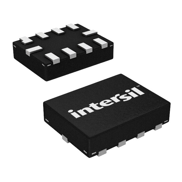
| 产品图片 |
|
| rohs | 符合RoHS无铅 / 符合限制有害物质指令(RoHS)规范要求 |
| 产品系列 | 数字电位计 IC,Intersil ISL90728WIE627Z-TKXDCP™ |
| 数据手册 | |
| 产品型号 | ISL90728WIE627Z-TK |
| POT数量 | Single |
| 产品目录页面 | |
| 产品种类 | 数字电位计 IC |
| 供应商器件封装 | SC-70-6 |
| 其它名称 | ISL90728WIE627Z-TK-ND |
| 包装 | 带卷 (TR) |
| 商标 | Intersil |
| 存储器类型 | 易失 |
| 安装类型 | 表面贴装 |
| 封装 | Reel |
| 封装/外壳 | 6-TSSOP,SC-88,SOT-363 |
| 封装/箱体 | SC-70 |
| 工作温度 | -40°C ~ 85°C |
| 工作电源电压 | 3.3 V |
| 工厂包装数量 | 1000 |
| 弧刷存储器 | Volatile |
| 抽头 | 128 |
| 接口 | I²C |
| 数字接口 | Serial (I2C) |
| 最大工作温度 | + 85 C |
| 最小工作温度 | - 40 C |
| 标准包装 | 1,000 |
| 每POT分接头 | 128 |
| 温度系数 | 标准值 ±45 ppm/°C |
| 电压-电源 | 2.7 V ~ 5.5 V |
| 电源电压-最大 | 5.5 V |
| 电源电压-最小 | 2.7 V |
| 电源电流 | 200 uA |
| 电路数 | 1 |
| 电阻 | 10 KOhms |
| 电阻(Ω) | 10k |
| 系列 | ISL90728 |


- 商务部:美国ITC正式对集成电路等产品启动337调查
- 曝三星4nm工艺存在良率问题 高通将骁龙8 Gen1或转产台积电
- 太阳诱电将投资9.5亿元在常州建新厂生产MLCC 预计2023年完工
- 英特尔发布欧洲新工厂建设计划 深化IDM 2.0 战略
- 台积电先进制程称霸业界 有大客户加持明年业绩稳了
- 达到5530亿美元!SIA预计今年全球半导体销售额将创下新高
- 英特尔拟将自动驾驶子公司Mobileye上市 估值或超500亿美元
- 三星加码芯片和SET,合并消费电子和移动部门,撤换高东真等 CEO
- 三星电子宣布重大人事变动 还合并消费电子和移动部门
- 海关总署:前11个月进口集成电路产品价值2.52万亿元 增长14.8%


PDF Datasheet 数据手册内容提取
DATASHEET ISL90727, ISL90728 FN8247 Single Volatile 128-Tap XDCP™ Digitally Controlled Potentiometer (XDCP) Rev 8.00 May 10, 2012 The Intersil ISL90727 and ISL90728 are digitally controlled Features potentiometers (XDCP™). Each device consists of a resistor • Volatile Solid-State Potentiometer array, wiper switches, and a control section. The wiper position is controlled by an I2C Bus™. • I2C Serial Bus Interface The potentiometer is implemented by a resistor array • DCP Terminal Voltage, 2.7V to 5.5V composed of 127 resistive elements and a wiper switching • Low Tempco network. Between each element and at either end are tap - Rheostat - 45 ppm/°C Typical points accessible to the wiper terminal. The position of the - Divider - 15 ppm/°C Typical wiper element is controlled by the SDA and SCL inputs. • 128 Wiper Tap Points Pinout - Wiper Resistance 70 Typ at VCC = 3.3V ISL90727, ISL90728 • Low Power CMOS (6 LD SC-70) - Active Current, 200µA Max TOP VIEW - Standby Current, 500nA Max VDD 1 6 RH • Available RTOTAL Values = 50k10k • Power-on Preset to Midscale GND 2 5 RW • Packaging SCL 3 4 SDA - 6 Ld SC-70 • Pb-Free (RoHS Compliant) Applications • Mechanical Potentiometer Replacement • Transducer Adjustment of Pressure, Temperature, Position, Chemical, and Optical Sensors • RF Amplifier Biasing • LCD Brightness and Contrast Adjustment • Gain Control and Offset Adjustment Ordering Information PART NUMBER PART MARKING RTOTAL TEMP RANGE PACKAGE PKG. (Notes 1, 2, 3, 4) (Bottom Side) (k) (°C) (Pb-Free) DWG. # ISL90727UIE627Z-TK ANI 50 -40 to +85 6 Ld SC-70 P6.049 ISL90727WIE627Z-T7A ANH 10 -40 to +85 6 Ld SC-70 P6.049 ISL90727WIE627Z-TK ANH 10 -40 to +85 6 Ld SC-70 P6.049 ISL90728UIE627Z-TK CDY 50 -40 to +85 6 Ld SC-70 P6.049 ISL90728WIE627Z-T7A CCF 10 -40 to +85 6 Ld SC-70 P6.049 ISL90728WIE627Z-TK CCF 10 -40 to +85 6 Ld SC-70 P6.049 NOTES: 1. Please refer to TB347 for details on reel specifications. 2. These Intersil Pb-free plastic packaged products employ special Pb-free material sets, molding compounds/die attach materials, and 100% matte tin plate plus anneal (e3 termination finish, which is RoHS compliant and compatible with both SnPb and Pb-free soldering operations). Intersil Pb-free products are MSL classified at Pb-free peak reflow temperatures that meet or exceed the Pb-free requirements of IPC/JEDEC J STD-020. 3. For Moisture Sensitivity Level (MSL), please see device information page for ISL90727, ISL90728. For more information on MSL please see Tech Brief TB363. 4. ISL90727 has an I2C address 5Ch and ISL90728 has an I2C address 7Ch. FN8247 Rev 8.00 Page 1 of 8 May 10, 2012
ISL90727, ISL90728 Pin Descriptions PIN NUMBER SYMBOL DESCRIPTION 1 VDD Supply Voltage 2 GND Ground 3 SCL Open drain Serial Clock input 4 SDA Open drain Serial Data I/O 5 RW Potentiometer Wiper Terminal 6 RH Potentiometer High Terminal Block Diagram VDD RH SCL I2C SDA INTERFACE RW WIPER REGISTER RL GND FN8247 Rev 8.00 Page 2 of 8 May 10, 2012
ISL90727, ISL90728 Absolute Maximum Ratings Thermal Information Storage Temperature. . . . . . . . . . . . . . . . . . . . . . . .-65°C to +150°C Thermal Resistance (Typical) JA (°C/W) JC (°C/W) Voltage at any Digital Interface Pin 6 Ld SC-70 Package (Notes 5, 6) . . . . 480 210 with Respect to VSS. . . . . . . . . . . . . . . . . . . . .-0.3V to VCC + 0.3 Pb-Free Reflow Profile. . . . . . . . . . . . . . . . . . . . . . . . .see link below VCC . . . . . . . . . . . . . . . . . . . . . . . . . . . . . . . . . . . . . . . .-0.3V to +7V http://www.intersil.com/pbfree/Pb-FreeReflow.asp Voltage at any DCP Pin with Respect to VSS . . . . . . . . . . . . . . . . . . . . . . . . . . . . -0.3V to VCC Recommended Operating Conditions IW (10s) . . . . . . . . . . . . . . . . . . . . . . . . . . . . . . . . . . . . . . . . . . ±6mA Latchup . . . . . . . . . . . . . . . . . . . . . . . . . . Class II, Level B at +85°C Industrial . . . . . . . . . . . . . . . . . . . . . . . . . . . . . . . . . .-40°C to +85°C ESD Rating VCC . . . . . . . . . . . . . . . . . . . . . . . . . . . . . . . . . . . . . . . .2.7V to 5.5V Human Body Model . . . . . . . . . . . . . . . . . . . . . . . . . . . . . . . . .2kV Power Rating of Each DCP. . . . . . . . . . . . . . . . . . . . . . . . . . . .5mW CAUTION: Do not operate at or near the maximum ratings listed for extended periods of time. Exposure to such conditions may adversely impact product reliability and result in failures not covered by warranty. NOTES: 5. JA is measured with the component mounted on a high effective thermal conductivity test board in free air. See Tech Brief TB379 for details. 6. For JC, the “case temp” location is taken at the package top center. Analog Specifications Over recommended operating conditions, unless otherwise stated. MIN TYP MAX SYMBOL PARAMETER TEST CONDITIONS (Note 19) (Note7) (Note 19) UNIT RTOTAL RH to RL Resistance W option 10 k U option 50 k RH to RL Resistance Tolerance -20 +20 % RW Wiper Resistance VCC = 3.3V @ +25°C 85 200 CH/CL/CW Potentiometer Capacitance 10/10/25 pF ILkgDCP Leakage on DCP Pins Voltage at pin from GND to VCC 0.1 µA VOLTAGE DIVIDER MODE INL Integral Non-linearity -1 ±0.2 1 LSB (Note8) DNL Differential Non-linearity Monotonic over all tap positions W option -1 ±0.1 1 LSB (Note8) U option -1 ±0.1 1 LSB (Note8) ZSerror Zero-scale Error W option 0 1 3 LSB (Note9) (Note8) U option 0 0.5 1 FSerror Full-scale Error W option -3 -1 0 LSB (Note10) (Note8) U option -1 -0.5 0 TCV (Note 16) Ratiometric Temperature Coefficient DCP Register set to 80 hex ±15 ppm/°C RESISTOR MODE RINL Integral Non-linearity DCP register set between 20 hex and FF hex. -2 ±0.25 2 MI (Note 14) Monotonic over all tap positions (Note11) RDNL Differential Non-linearity DCP register set between 20 hex W option -1 ±0.1 1 MI (Note13) and FF hex. Monotonic over all tap (Note11) positions U option -1 ±0.1 1 MI (Note11) ROFFSET Offset W option 0 1 3 MI (Note12) (Note11) U option 0 0.5 1 MI (Note11) TCR Resistance Temperature Coefficient DCP register set between 20 hex and FF hex ±45 ppm/°C (Notes15, 16) FN8247 Rev 8.00 Page 3 of 8 May 10, 2012
ISL90727, ISL90728 Operating Specifications MIN TYP MAX SYMBOL PARAMETER TEST CONDITIONS (Note 19) (Note7) (Note 19) UNIT ICC1 VCC Supply Current fSCL = 400kHz; SDA = Open; (for I2C, Active, 200 µA (Volatile write/read) Read and Volatile Write States only) ISB VCC Current (standby) VCC = +5.5V, I2C Interface in Standby State 500 nA IComLkg Common-Mode Leakage Voltage at SDA pin to GND or VCC 3 µA tDCP (Note16) DCP Wiper Response Time SCL falling edge of last bit of DCP Data Byte to 500 ns wiper change VCCRamp VCC Ramp Rate 0.2 V/ms (Note20) tD Power-up Delay VCC above VPOR, to DCP Initial Value Register 3 ms recall completed, and I2C Interface in standby state SERIAL INTERFACE SPECIFICATIONS VIL SDA, and SCL Input Buffer LOW (Note 17) -0.3 0.3* V Voltage VCC VIH SDA, and SCL Input Buffer HIGH (Note 17) 0.7* VCC+ V Voltage VCC 0.3 Hysteresis SDA and SCL Input Buffer Hysteresis 0.05* V VCC VOL SDA Output Buffer LOW Voltage, 0 0.4 V Sinking 4mA Cpin (Note18) SDA and SCL Pin Capacitance 10 pF fSCL SCL Frequency 400 kHz tIN Pulse Width Suppression Time at Any pulse narrower than the max spec is 50 ns SDA and SCL Inputs suppressed. tAA SCL Falling Edge to SDA Output Data SCL falling edge crossing 30% of VCC, until SDA 900 ns Valid exits the 30% to 70% of VCC window. tBUF Time the Bus Must be Free Before the SDA crossing 70% of VCC during a STOP 1300 ns Start of a New Transmission condition, to SDA crossing 70% of VCC during the following START condition. tLOW Clock LOW Time Measured at the 30% of VCC crossing. 1300 ns tHIGH Clock HIGH Time Measured at the 70% of VCC crossing. 600 ns tSU:STA START Condition Setup Time SCL rising edge to SDA falling edge. Both 600 ns crossing 70% of VCC. tHD:STA START Condition Hold Time From SDA falling edge crossing 30% of VCC to 600 ns SCL falling edge crossing 70% of VCC. tSU:DAT Input Data Setup Time From SDA exiting the 30% to 70% of VCC 100 ns window, to SCL rising edge crossing 30% of VCC tHD:DAT Input Data Hold Time From SCL rising edge crossing 70% of VCC to 0 ns SDA entering the 30% to 70% of VCC window. tSU:STO STOP Condition Setup Time From SCL rising edge crossing 70% of VCC, to 600 ns SDA rising edge crossing 30% of VCC. tHD:STO STOP Condition Hold Time for Read, From SDA rising edge to SCL falling edge. Both 600 ns or Volatile Only Write crossing 70% of VCC. tDH Output Data Hold Time From SCL falling edge crossing 30% of VCC, 0 ns until SDA enters the 30% to 70% of VCC window. tR (Note18) SDA and SCL Rise Time From 30% to 70% of VCC 20 + 250 ns 0.1*Cb FN8247 Rev 8.00 Page 4 of 8 May 10, 2012
ISL90727, ISL90728 Operating Specifications (Continued) MIN TYP MAX SYMBOL PARAMETER TEST CONDITIONS (Note 19) (Note7) (Note 19) UNIT tF (Note18) SDA and SCL Fall Time From 70% to 30% of VCC 20 + 250 ns 0.1*Cb Cb (Note18) Capacitive Loading of SDA or SCL Total on-chip and off-chip 10 400 pF Rpu (Note18) SDA and SCL Bus Pull-up Resistor Maximum is determined by tR and tF. 1 k Off-chip For Cb = 400pF, max is about 2k~ 2.5k. For Cb = 40pF, max is about 15k~ 20k NOTES: 7. Typical values are for TA = +25°C and 3.3V supply voltage. 8. LSB: [V(RW)127 – V(RW)0]/127. V(RW)127 and V(RW)0 are V(RW) for the DCP register set to FF hex and 00 hex respectively. LSB is the incremental voltage when changing from one tap to an adjacent tap. 9. ZS error = V(RW)0/LSB. 10. FS error = [V(RW)127 – VCC]/LSB. 11. MI = |R127 – R0|/127. R127 and R0 are the measured resistances for the DCP register set to FF hex and 00 hex respectively. ROFFSET = R0/MI, when measuring between RW and RL. 12. ROFFSET = R127/MI, when measuring between RW and RH. 13. RDNL = (Ri – Ri-1)/MI - 1, for i = 32 to 127. 14. RINL = [Ri – (MI • i) – R0]/MI, for i = 32 to 127. 6 MaxRi–MinRi 10 15.TC = -------------------------------------------------------------------------------------for i = 32 to 127, T = -40°C to +85°C. Max( ) is the maximum value of the resistance and Min ( ) is the R MaxRi+MinRi2 +125°Cminimum value of the resistance over the temperature range. 16. This parameter is not 100% tested. 17. VIL = 0V, VIH = VCC. 18. These are I2C-specific parameters and are not directly tested, however, they are used in the device testing to validate specifications. 19. Parameters with MIN and/or MAX limits are 100% tested at +25°C, unless otherwise specified. Temperature limits established by characterization and are not production tested. 20. The ramp must be >0.2V/ms at any voltage <2.7V starting from 0VDC. A power down to any voltage other than 0V is not included in the ramp rate spec and may result in improper operation. SDA vs SCL Timing tF tHIGH tLOW tR SCL tSU:DAT tSU:STA tHD:DAT tSU:STO tHD:STA SDA (INPUT TIMING) tAA tDH tBUF SDA (OUTPUT TIMING) FN8247 Rev 8.00 Page 5 of 8 May 10, 2012
ISL90727, ISL90728 Principles of Operation command until this condition is met (see Figure 1). A START condition is ignored during the power-up sequence and during The ISL90727 and ISL90728 are integrated circuits incorporating one DCP with its associated registers and an I2C internal non-volatile write cycles. serial interface providing direct communication between a host All I2C interface operations must be terminated by a STOP and the potentiometer. condition, which is a LOW to HIGH transition of SDA while SCL is HIGH (see Figure 1). DCP Description The DCP is implemented with a combination of resistor elements An ACK, Acknowledge, is a software convention used to and CMOS switches. The physical ends of the DCP are indicate a successful data transfer. The transmitting device, equivalent to the fixed terminals of a mechanical potentiometer either master or slave, releases the SDA bus after transmitting (RH and RL pins). The RW pin of the DCP is connected to 8 bits. During the ninth clock cycle, the receiver pulls the SDA intermediate nodes, and is equivalent to the wiper terminal of a line LOW to acknowledge the reception of the eight bits of data mechanical potentiometer. The position of the wiper terminal (see Figure 2). within the DCP is controlled by a 7-bit volatile Wiper Register The ISL90727 and ISL90728 respond with an ACK after (WR). The DCP has its own WR. When the WR of the DCP recognition of a START condition followed by a valid contains all zeroes (WR<6:0> = 00h), its wiper terminal (RW) is Identification Byte, and once again after successful receipt of closest to its “Low” terminal (RL). When the WR of the DCP an Address Byte. The ISL90727 and ISL90728 also respond contains all ones (WR<6:0> = 7Fh), its wiper terminal (RW) is with an ACK after receiving a Data Byte of a write operation. closest to its “High” terminal (RH). As the value of the WR The master must respond with an ACK after receiving a Data increases from all zeroes (00h) to all ones (127 decimal), the Byte of a read operation. wiper moves monotonically from the position closest to RL to the position closest to RH. At the same time, the resistance between A valid Identification Byte contains 0101110 as the seven RW and RL increases monotonically, while the resistance MSBs for the ISL90727 and 0111110 as the seven MSBs for between RH and RW decreases monotonically. RL is connected the ISL90728. The LSB in the Read/Write bit. Its value is “1” for to the GND pin of the device, so the wiper movement will always a Read operation, and “0” for a Write operation (see Table 1). be relative to RL. TABLE 1. IDENTIFICATION BYTE FORMAT While the ISL90727 and ISL90728 are being powered up, the ISL90727 0 1 0 1 1 1 0 R/W WR is reset to 40h (64 decimal), which locates RW roughly at ISL90728 0 1 1 1 1 1 0 R/W the center between RL and RH. MSB LSB The WR and IVR can be read or written directly using the I2C serial interface as described in the following sections. Write Operation 2 I C Serial Interface A Write operation requires a START condition, followed by a valid Identification Byte, a valid Address Byte, a Data Byte, and The ISL90727 and ISL90728 support bidirectional bus oriented a STOP condition. After each of the three bytes, the ISL90727 protocol. The protocol defines any device that sends data onto and ISL90728 respond with an ACK. At this time, the device the bus as a transmitter and the receiving device as the enters its standby state (see Figure 3). receiver. The device controlling the transfer is a master and the device being controlled is the slave. The master always Data Protection initiates data transfers and provides the clock for both transmit A valid Identification Byte, Address Byte, and total number of and receive operations. Therefore, the ISL90727 and SCL pulses act as a protection of both volatile and non-volatile ISL90728 operate as slave devices in all applications. registers. During a Write sequence, the Data Byte is loaded All communication over the I2C interface is conducted by into an internal shift register as it is received. If the Address sending the MSB of each byte of data first. Byte is 0, the Data Byte is transferred to the Wiper Register (WR) at the falling edge of the SCL pulse that loads the last bit Protocol Conventions (LSB) of the Data Byte. If an address other than 00h or an Data states on the SDA line can change only during SCL LOW invalid slave address is sent, then the device will respond with periods. SDA state changes during SCL HIGH are reserved for no ACK. indicating START and STOP conditions (see Figure 1). On power-up of the ISL90727 and ISL90728, the SDA pin is in the Read Operation input mode. A Read operation consist of a three byte instruction followed by All I2C interface operations must begin with a START condition, one or more Data Bytes (See Figure 4). The master initiates which is a HIGH to LOW transition of SDA while SCL is HIGH. the operation issuing the following sequence: a START, the The ISL90727 and ISL90728 continuously monitor the SDA and Identification byte with the R/W bit set to “0”, an Address Byte, SCL lines for the START condition and do not respond to any a second START, and a second Identification byte with the R/W FN8247 Rev 8.00 Page 6 of 8 May 10, 2012
ISL90727, ISL90728 bit set to “1”. After each of the three bytes, the ISL90727 and operation (issuing a STOP condition) following the last bit of ISL90728 respond with an ACK. Then the ISL90727 and the Data Byte (see Figure 4). ISL90728 transmit the Data Byte as long as the master responds with an ACK during the SCL cycle following the eighth bit of each byte. The master then terminates the read SCL SDA START DATA DATA DATA STOP STABLE CHANGE STABLE FIGURE 1. VALID DATA CHANGES, START AND STOP CONDITIONS SCL FROM MASTER 1 8 9 SDA OUTPUT FROM HIGH IMPEDANCE TRANSMITTER SDA OUTPUT FROM HIGH IMPEDANCE RECEIVER START ACK FIGURE 2. ACKNOWLEDGE RESPONSE FROM RECEIVER WRITE S SIGNALS FROM T S THE MASTER A IDENTIFICATION ADDRESS DATA T R BYTE BYTE BYTE O T P SIGNAL AT SDA 0 1 0 1 1 1 0 0 0 0 0 00 00 0 0 0 SIGNALS FROM A A A THE ISL23711 C C C K K K FIGURE 3. BYTE WRITE SEQUENCE (ISL90727 VERSION SHOWN) S S SIGNALS T T S FROM THE A IDENTIFICATION A IDENTIFICATION T MASTER R BYTE WITH ADDRESS R BYTE WITH O T R/W = 0 BYTE T R/W = 1 P SIGNAL AT SDA 0 1 0 1 1 1 0 0 0 0 0 0 0 0 0 0 0 1 0 1 1 1 0 1 A A A SIGNALS FROM C C C DATA BYTE THE SLAVE K K K FIGURE 4. READ SEQUENCE (ISL90727 VERSION SHOWN) FN8247 Rev 8.00 Page 7 of 8 May 10, 2012
ISL90727, ISL90728 Small Outline Transistor Plastic Packages (SC70-6) 0.20 (0.008) M C VIEW C P6.049 CL 6 LEAD SMALL OUTLINE TRANSISTOR PLASTIC PACKAGE b e INCHES MILLIMETERS SYMBOL MIN MAX MIN MAX NOTES 6 5 4 A 0.031 0.043 0.80 1.10 - CL E1 A1 0.000 0.004 0.00 0.10 - CL E A2 0.031 0.039 0.00 1.00 - 1 2 3 b 0.006 0.012 0.15 0.30 - 8 PIN 1 b1 0.006 0.010 0.15 0.25 INDEX AREA e1 c 0.003 0.009 0.08 0.22 6 C D c1 0.003 0.009 0.08 0.20 6 D 0.073 0.085 1.85 2.15 3 CL E 0.071 0.094 1.80 2.40 - E1 0.045 0.053 1.15 1.35 3 SEATING A A2 A1 PLANE e 0.0256 Ref 0.65 Ref - -C- e1 0.0512 Ref 1.30 Ref - L 0.010 0.018 0.26 0.46 4 0.10 (0.004) C L1 0.017 Ref. 0.420 Ref. L2 0.006 BSC 0.15 BSC b WITH N 6 6 5 PLATING b1 R 0.004 - 0.10 - R1 0.004 0.010 0.15 0.25 c c1 0o 8o 0o 8o - BASE METAL Rev. 3 4/12 NOTES: 1. Dimensioning and tolerance per ASME Y14.5M-1994. 4X 1 2. Package conforms to EIAJ SC70 and JEDEC MO203AB. 3. Dimensions D and E1 are exclusive of mold flash, protrusions, R1 or gate burrs. 4. Footlength L measured at reference to gauge plane. R 5. “N” is the number of terminal positions. GAUGE PLANE 6. These Dimensions apply to the flat section of the lead between SEATING L 0.08mm and 0.15mm from the lead tip. PLANE C 7. Controlling dimension: MILLIMETER. Converted inch dimen- L1 L2 sions are for reference only. 4X 1 8. The configuration of the pin #1 identifier is optional, but must be VIEW C located within the zone indicated. The pin #1 identifier may be either a mold or mark feature. © Copyright Intersil Americas LLC 2005-2012. All Rights Reserved. All trademarks and registered trademarks are the property of their respective owners. For additional products, see www.intersil.com/en/products.html Intersil products are manufactured, assembled and tested utilizing ISO9001 quality systems as noted in the quality certifications found at www.intersil.com/en/support/qualandreliability.html Intersil products are sold by description only. Intersil may modify the circuit design and/or specifications of products at any time without notice, provided that such modification does not, in Intersil's sole judgment, affect the form, fit or function of the product. Accordingly, the reader is cautioned to verify that datasheets are current before placing orders. Information furnished by Intersil is believed to be accurate and reliable. However, no responsibility is assumed by Intersil or its subsidiaries for its use; nor for any infringements of patents or other rights of third parties which may result from its use. No license is granted by implication or otherwise under any patent or patent rights of Intersil or its subsidiaries. For information regarding Intersil Corporation and its products, see www.intersil.com FN8247 Rev 8.00 Page 8 of 8 May 10, 2012