ICGOO在线商城 > 集成电路(IC) > 数据采集 - 数字电位器 > ISL23415WFUZ

 Datasheet下载
- 型号: ISL23415WFUZ
- 制造商: Intersil
- 库位|库存: xxxx|xxxx
- 要求:
| 数量阶梯 | 香港交货 | 国内含税 |
| +xxxx | $xxxx | ¥xxxx |
查看当月历史价格
查看今年历史价格
ISL23415WFUZ产品简介:
ICGOO电子元器件商城为您提供ISL23415WFUZ由Intersil设计生产,在icgoo商城现货销售,并且可以通过原厂、代理商等渠道进行代购。 ISL23415WFUZ价格参考。IntersilISL23415WFUZ封装/规格:数据采集 - 数字电位器, Digital Potentiometer 10k Ohm 1 Circuit 256 Taps SPI Interface 10-MSOP。您可以下载ISL23415WFUZ参考资料、Datasheet数据手册功能说明书,资料中有ISL23415WFUZ 详细功能的应用电路图电压和使用方法及教程。
ISL23415WFUZ是由Renesas Electronics America Inc.生产的数字电位器,广泛应用于需要精确控制和调节电阻值的场合。以下是该型号的主要应用场景:

 1. 音频设备
在音频设备中,ISL23415WFUZ可以用于音量控制、平衡调整等场景。通过数字接口调节电位器的阻值,用户可以实现无噪声的音量调节,避免了传统机械电位器带来的磨损和噪音问题。

 2. 工业自动化
在工业控制系统中,ISL23415WFUZ可用于调节传感器信号的增益或偏置电压。例如,在温度、压力或湿度传感器的应用中,可以通过数字电位器来微调传感器的输出信号,确保测量结果的准确性。此外,它还可以用于PID控制器中的参数调节,提高系统的响应速度和稳定性。

 3. 医疗设备
医疗设备对精度和可靠性要求极高。ISL23415WFUZ可以用于心电图机、血压计等设备中的信号调理电路,确保信号的准确性和稳定性。此外,它还可以用于医疗仪器中的校准功能,帮助技术人员快速、精确地调整设备参数。

 4. 通信设备
在通信系统中,ISL23415WFUZ可用于调节发射功率、接收灵敏度等关键参数。例如,在无线通信模块中,数字电位器可以动态调整射频前端的增益,优化信号传输质量,减少干扰和失真。

 5. 消费电子产品
在消费电子产品中,ISL23415WFUZ可以用于显示器的亮度调节、对比度控制等。通过数字接口控制电位器的阻值,用户可以实现平滑的调节效果,提升用户体验。此外,它还可以用于智能家居设备中的传感器校准,确保设备的正常工作。

 6. 汽车电子
在汽车电子系统中,ISL23415WFUZ可以用于车载音响系统的音量控制、均衡器调节等。此外,它还可以用于发动机管理系统中的传感器信号调理,确保传感器数据的准确性和稳定性,从而提高车辆的整体性能。

总之,ISL23415WFUZ凭借其高精度、低功耗和可靠的性能,适用于多种需要精确电阻调节的应用场景,特别是在对精度和可靠性要求较高的领域中表现出色。
| 参数 | 数值 |
| 产品目录 | 集成电路 (IC) |
| 描述 | IC DGTL POT 256POS 10K 10MSOP |
| 产品分类 | |
| 品牌 | Intersil |
| 数据手册 | |
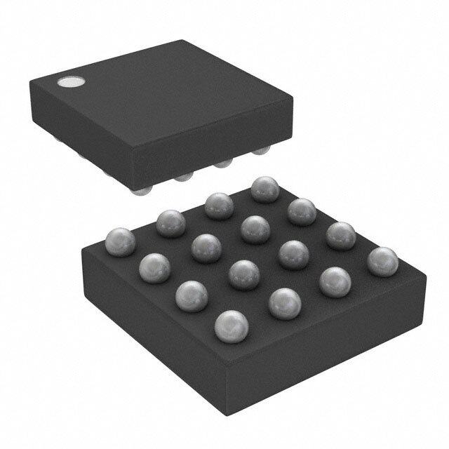
| 产品图片 |
|
| 产品型号 | ISL23415WFUZ |
| rohs | 无铅 / 符合限制有害物质指令(RoHS)规范要求 |
| 产品系列 | XDCP™ |
| 产品培训模块 | http://www.digikey.cn/PTM/IndividualPTM.page?site=cn&lang=zhs&ptm=25593 |
| 供应商器件封装 | 10-MSOP |
| 包装 | 管件 |
| 存储器类型 | 易失 |
| 安装类型 | 表面贴装 |
| 封装/外壳 | 10-TFSOP,10-MSOP(0.118",3.00mm 宽) |
| 工作温度 | -40°C ~ 125°C |
| 抽头 | 256 |
| 接口 | 4 线 SPI(芯片选择) |
| 标准包装 | 50 |
| 温度系数 | 标准值 175 ppm/°C |
| 电压-电源 | 1.2 V ~ 5.5 V,1.7 V ~ 5.5 V |
| 电路数 | 1 |
| 电阻(Ω) | 10k |


- 商务部:美国ITC正式对集成电路等产品启动337调查
- 曝三星4nm工艺存在良率问题 高通将骁龙8 Gen1或转产台积电
- 太阳诱电将投资9.5亿元在常州建新厂生产MLCC 预计2023年完工
- 英特尔发布欧洲新工厂建设计划 深化IDM 2.0 战略
- 台积电先进制程称霸业界 有大客户加持明年业绩稳了
- 达到5530亿美元!SIA预计今年全球半导体销售额将创下新高
- 英特尔拟将自动驾驶子公司Mobileye上市 估值或超500亿美元
- 三星加码芯片和SET,合并消费电子和移动部门,撤换高东真等 CEO
- 三星电子宣布重大人事变动 还合并消费电子和移动部门
- 海关总署:前11个月进口集成电路产品价值2.52万亿元 增长14.8%


PDF Datasheet 数据手册内容提取
DATASHEET ISL23415 FN7780 Single, Low Voltage Digitally Controlled Potentiometer (XDCP™) Rev 2.00 September 14, 2015 The ISL23415 is a volatile, low voltage, low noise, low power, Features SPI™ bus, 256 taps, single digitally controlled potentiometer (DCP), which integrates DCP core, wiper switches and control • 256 resistor taps logic on a monolithic CMOS integrated circuit. • SPI serial interface - No additional level translator for low bus supply The digitally controlled potentiometer is implemented with a combination of resistor elements and CMOS switches. The - Daisy Chaining of multiple DCP position of the wipers are controlled by the user through the • Power supply SPI bus interface. The potentiometer has an associated volatile Wiper Register (WR) that can be directly written to and - VCC = 1.7V to 5.5V analog power supply read by the user. The contents of the WR controls the position - VLOGIC = 1.2V to 5.5V SPI bus/logic power supply of the wiper. When powered on, the ISL23415’s wiper will • Wiper resistance: 70 typical @ VCC = 3.3V always commence at mid-scale (128 tap position). • Shutdown Mode - forces the DCP into an end-to-end open The low voltage, low power consumption, and small package circuit and RW is shorted to RL internally of the ISL23415 make it an ideal choice for use in battery • Power-on preset to mid-scale (128 tap position) operated equipment. In addition, the ISL23415 has a VLOGIC pin allowing down to 1.2V bus operation, independent from the • Shutdown and standby current <2.8µA max VCC value. This allows for low logic levels to be connected • DCP terminal voltage from 0V to VCC directly to the ISL23415 without passing through a voltage • 10k 50kor 100k total resistance level shifter. • Extended industrial temperature range: -40°C to +125°C The DCP can be used as a three-terminal potentiometer or as a two-terminal variable resistor in a wide variety of applications • 10 Ld MSOP or 10 Ld µTQFN packages including control, parameter adjustments, and signal • Pb-free (RoHS compliant) processing. Applications • Power supply margining • RF power amplifier bias compensation • LCD bias compensation • Gain adjustment in battery powered instruments • Portable medical equipment calibration 10000 8000 Ω) E ( 6000 C N A T S SI 4000 E R 2000 0 0 50 100 150 200 250 TAP POSITION (DECIMAL) FIGURE 1. FORWARD AND BACKWARD RESISTANCE vs TAP FIGURE 2. VREF ADJUSTMENT POSITION, 10k FN7780 Rev 2.00 Page 1 of 20 September 14, 2015
ISL23415 Block Diagram VLOGIC VCC SCK RH POWER-UP SDI INTERFACE, SDO I/O BLOCK SLHEIFVTEELR COANNTDROL VOLWARTILE CS STATUS REGISTER LOGIC AND WIPER CONTROL CIRCUITRY RL RW GND Pin Configurations Pin Descriptions ISL23415 (10 LD MSOP) MSOP µTQFN SYMBOL DESCRIPTION TOP VIEW VLOGIC 1 O 10 GND 1 10 VLOGIC SRPaIn bgue s1/.l2oVgi cto s 5u.p5pVly. SCK 2 9 VCC 2 1 SCK Logic Pin - Serial bus clock input SDO 3 8 RH 3 2 SDO Logic Pin - Serial bus data output SDI 4 7 RW (configurable) CS 5 6 RL 4 3 SDI Logic Pin - Serial bus data input 5 4 CS Logic Pin - Active low Chip Select ISL23415 (10 LD µTQFN) 6 5 RL DCP “low” terminal TOP VIEW 7 6 RW DCP wiper terminal C GI 8 7 RH DCP “high” terminal O L V 9 8 VCC Analog power supply. O 10 Range 1.7V to 5.5V SCK 1 9 GND 10 9 GND Ground pin SDO 2 8 VCC SDI 3 7 RH CS 4 6 RW 5 L R FN7780 Rev 2.00 Page 2 of 20 September 14, 2015
ISL23415 Ordering Information RESISTANCE PART NUMBER PART OPTION TEMP. RANGE PACKAGE PKG. (Note 5) MARKING (kΩ) (°C) (Pb-free) DWG. # ISL23415TFUZ (Notes 1, 3) 3415T 100 -40 to +125 10 Ld MSOP M10.118 ISL23415UFUZ (Notes 1, 3) (No longer 3415U 50 -40 to +125 10 Ld MSOP M10.118 available, Recommended Replacement ISL23415WFUZ-TK) ISL23415WFUZ (Notes 1, 3) 3415W 10 -40 to +125 10 Ld MSOP M10.118 ISL23415TFRUZ-T7A (Notes 2, 4) HE 100 -40 to +125 10 Ld µTQFN 2.1x1.6 L10.2.1x1.6A ISL23415TFRUZ-TK (Notes 2, 4) HE 100 -40 to +125 10 Ld µTQFN 2.1x1.6 L10.2.1x1.6A ISL23415UFRUZ-T7A (Notes 2, 4) (No HD 50 -40 to +125 10 Ld µTQFN 2.1x1.6 L10.2.1x1.6A longer available, Recommended Replacement ISL23415WFUZ-TK) ISL23415WFRUZ-T7A (Notes 2, 4) (No HC 10 -40 to +125 10 Ld µTQFN 2.1x1.6 L10.2.1x1.6A longer available, Recommended Replacement ISL23415WFUZ-TK) NOTES: 1. Add “-TK” or “-T7A” suffix for Tape and Reel option. Please refer to TB347 for details on reel specifications. 2. Please refer to TB347 for details on reel specifications. 3. These Intersil Pb-free plastic packaged products employ special Pb-free material sets, molding compounds/die attach materials, and 100% matte tin plate plus anneal (e3 termination finish, which is RoHS compliant and compatible with both SnPb and Pb-free soldering operations). Intersil Pb-free products are MSL classified at Pb-free peak reflow temperatures that meet or exceed the Pb-free requirements of IPC/JEDEC J STD-020. 4. These Intersil Pb-free plastic packaged products employ special Pb-free material sets; molding compounds/die attach materials and NiPdAu plate-e4 termination finish, which is RoHS compliant and compatible with both SnPb and Pb-free soldering operations. Intersil Pb-free products are MSL classified at Pb-free peak reflow temperatures that meet or exceed the Pb-free requirements of IPC/JEDEC J STD-020. 5. For Moisture Sensitivity Level (MSL), please see device information page for ISL23415. For more information on MSL please see techbrief TB363. FN7780 Rev 2.00 Page 3 of 20 September 14, 2015
ISL23415 Absolute Maximum Ratings Thermal Information Supply Voltage Range Thermal Resistance (Typical) JA (°C/W) JC (°C/W) VCC . . . . . . . . . . . . . . . . . . . . . . . . . . . . . . . . . . . . . . . . . . . . . . . . -0.3V to 6.0V 10 Ld MSOP Package (Note 6, 7). . . . . . . . 170 70 VLOGIC . . . . . . . . . . . . . . . . . . . . . . . . . . . . . . . . . . . . . . . . . . . . . -0.3V to 6.0V 10 Ld µTQFN Package (Note 6, 7) . . . . . . . 145 90 Voltage on any DCP Terminal Pin. . . . . . . . . . . . . . . . . . . . . . . -0.3V to 6.0V Maximum Junction Temperature (Plastic Package) . . . . . . . . . . . .+150°C Voltage on any Digital Pins . . . . . . . . . . . . . . . . . . . . . . . . . . . . -0.3V to 6.0V Storage Temperature Range. . . . . . . . . . . . . . . . . . . . . . . .-65°C to +150°C Wiper Current IW (10s). . . . . . . . . . . . . . . . . . . . . . . . . . . . . . . . . . . . . . ±6mA Pb-Free Reflow Profile . . . . . . . . . . . . . . . . . . . . . . . . . . . . . . . see link below ESD Rating http://www.intersil.com/pbfree/Pb-FreeReflow.asp Human Body Model (Tested per JESD22-A114E). . . . . . . . . . . . . . .6.5kV CDM Model (Tested per JESD22-A114E). . . . . . . . . . . . . . . . . . . . . . . 1kV Recommended Operating Conditions Machine Model (Tested per JESD22-A115-A). . . . . . . . . . . . . . . . . .200V Latch Up Temperature . . . . . . . . . . . . . . . . . . . . . . . . . . . . . . . . . . . . .-40°C to +125°C (Tested per JESD-78B; Class 2, Level A) . . . . . . . . . . 100mA @ +125°C VCC Supply Voltage. . . . . . . . . . . . . . . . . . . . . . . . . . . . . . . . . . . .1.7V to 5.5V VLOGIC Supply Voltage. . . . . . . . . . . . . . . . . . . . . . . . . . . . . . . . .1.2V to 5.5V DCP Terminal Voltage . . . . . . . . . . . . . . . . . . . . . . . . . . . . . . . . . . . . .0 to VCC Max Wiper Current . . . . . . . . . . . . . . . . . . . . . . . . . . . . . . . . . . . . . . . . . ±3mA CAUTION: Do not operate at or near the maximum ratings listed for extended periods of time. Exposure to such conditions may adversely impact product reliability and result in failures not covered by warranty. NOTES: 6. is measured with the component mounted on a high effective thermal conductivity test board in free air. See Tech Brief TB379 for details. JA 7. For JC, the “case temp” location is the center top of the package. Analog Specifications VCC = 2.7V to 5.5V, VLOGIC = 1.2V to 5.5V over recommended operating conditions unless otherwise stated. Boldface limits apply over the operating temperature range, -40°Cto+125°C. MIN TYP MAX SYMBOL PARAMETER TEST CONDITIONS (Note 20) (Note8) (Note 20) UNITS RTOTAL RH to RL Resistance W option 10 kΩ U option 50 kΩ T option 100 kΩ RH to RL Resistance Tolerance -20 ±2 +20 % End-to-End Temperature Coefficient W option 175 ppm/°C U option 85 ppm/°C T option 70 ppm/°C VRH, VRL DCP Terminal Voltage VRH or VRL to GND 0 VCC V RW Wiper Resistance RH - floating, VRL = 0V, force IW current 70 200 Ω to the wiper, IW = (VCC - VRL)/RTOTAL, VCC = 2.7V to 5.5V VCC = 1.7V 580 Ω CH/CL/CW Terminal Capacitance See “DCP Macro Model” on page8. 32 pF ILkgDCP Leakage on DCP Pins Voltage at pin from GND to VCC -0.4 <0.1 0.4 µA Noise Resistor Noise Density Wiper at middle point, W option 16 nV/√Hz Wiper at middle point, U option 49 nV/√Hz Wiper at middle point, T option 61 nV/√Hz Feed Thru Digital Feedthrough from Bus to Wiper Wiper at middle point -65 dB PSRR Power Supply Reject Ratio Wiper output change if VCC change -75 dB ±10%; wiper at middle point FN7780 Rev 2.00 Page 4 of 20 September 14, 2015
ISL23415 Analog Specifications VCC = 2.7V to 5.5V, VLOGIC = 1.2V to 5.5V over recommended operating conditions unless otherwise stated. Boldface limits apply over the operating temperature range, -40°Cto+125°C. (Continued) MIN TYP MAX SYMBOL PARAMETER TEST CONDITIONS (Note 20) (Note8) (Note 20) UNITS VOLTAGE DIVIDER MODE (0V @ RL; VCC @ RH; measured at RW, unloaded) INL Integral Non-linearity, Guaranteed W option -1.0 ±0.5 +1.0 LSB (Note 13) Monotonic (Note 9) U, T option -0.5 ±0.15 +0.5 LSB (Note 9) DNL Differential Non-linearity, Guaranteed W option -1 ±0.4 +1 LSB (Note 12) Monotonic (Note 9) U, T option -0.4 ±0.1 +0.4 LSB (Note 9) FSerror Full-scale Error W option -3.5 -2 0 LSB (Note 11) (Note 9) U, T option -2 -0.5 0 LSB (Note 9) ZSerror Zero-scale Error W option 0 2 3.5 LSB (Note 10) (Note 9) U, T option 0 0.4 2 LSB (Note 9) TCV Ratiometric Temperature Coefficient W option, Wiper Register set to 80 hex 8 ppm/°C (Note 14) U option, Wiper Register set to 80 hex 4 ppm/°C T option, Wiper Register set to 80 hex 2.3 ppm/°C Large Signal Wiper Settling Time From code 0 to FF hex 300 ns fcutoff -3dB Cutoff Frequency Wiper at middle point W option 1200 kHz Wiper at middle point U option 250 kHz Wiper at middle point T option 120 kHz RHEOSTAT MODE (Measurements between RW and RL pins with RH not connected, or between RW and RH with RL not connected) RINL Integral Non-linearity, Guaranteed W option; VCC = 2.7V to 5.5V -2.0 ±1 +2.0 MI (Note 18) Monotonic (Note 15) W option; VCC = 1.7V 10.5 MI (Note 15) U, T option; VCC = 2.7V to 5.5V -1.0 ±0.3 +1.0 MI (Note 15) U, T option; VCC = 1.7V 2.1 MI (Note 15) RDNL Differential Non-linearity, Guaranteed W option; VCC = 2.7V to 5.5V -1 ±0.4 +1 MI (Note 17) Monotonic (Note 15) W option; VCC = 1.7V ±0.6 MI (Note 15) U, T option; VCC = 2.7V to 5.5V -0.5 ±0.15 +0.5 MI (Note 15) U, T option; VCC = 1.7V ±0.35 MI (Note 15) FN7780 Rev 2.00 Page 5 of 20 September 14, 2015
ISL23415 Analog Specifications VCC = 2.7V to 5.5V, VLOGIC = 1.2V to 5.5V over recommended operating conditions unless otherwise stated. Boldface limits apply over the operating temperature range, -40°Cto+125°C. (Continued) MIN TYP MAX SYMBOL PARAMETER TEST CONDITIONS (Note 20) (Note8) (Note 20) UNITS Roffset Offset, Wiper at 0 Position W option; VCC = 2.7V to 5.5V 0 3 5.5 MI (Note 16) (Note 15) W option; VCC = 1.7V 6.3 MI (Note 15) U, T option; VCC = 2.7V to 5.5V 0 0.5 2 MI (Note 15) U, T option; VCC = 1.7V 1.1 MI (Note 15) TCR Resistance Temperature Coefficient W option; Wiper register set between 220 ppm/°C (Note 19) 32 hex and FF hex U option; Wiper register set between 100 ppm/°C 32 hex and FF hex T option; Wiper register set between 32 75 ppm/°C hex and FF hex Operating Specifications VCC = 2.7V to 5.5V, VLOGIC = 1.2V to 5.5V over recommended operating conditions unless otherwise stated. Boldface limits apply over the operating temperature range, -40°Cto+125°C. MIN TYP MAX SYMBOL PARAMETER TEST CONDITIONS (Note 20) (Note8) (Note 20) UNITS ILOGIC VLOGIC Supply Current (Write/Read) VLOGIC = 5.5V, VCC = 5.5V, 1.5 mA fSCK = 5MHz (for SPI active read and write) VLOGIC = 1.2V, VCC = 1.7V, 30 µA fSCK = 1MHz (for SPI active read and write) ICC VCC Supply Current (Write/Read) VLOGIC = 5.5V, VCC = 5.5V 100 µA VLOGIC = 1.2V, VCC = 1.7V 10 µA ILOGIC SB VLOGIC Standby Current VLOGIC = 5.5V, VCC = 5.5V, 1.3 µA SPI interface in standby VLOGIC = 1.2V, VCC = 1.7V, 0.4 µA SPI interface in standby ICC SB VCC Standby Current VLOGIC = 5.5V, VCC = 5.5V, 1.5 µA SPI interface in standby VLOGIC = 1.2V, VCC = 1.7V, 1 µA SPI interface in standby ILOGIC SHDN VLOGIC Shutdown Current VLOGIC = 5.5V, VCC = 5.5V, 1.3 µA SPI interface in standby VLOGIC = 1.2V, VCC = 1.7V, 0.4 µA SPI interface in standby ICC SHDN VCC Shutdown Current VLOGIC = VCC = 5.5V, 1.5 µA SPI interface in standby VLOGIC = 1.2V, VCC = 1.7V, 1 µA SPI interface in standby ILkgDig Leakage Current, at Pins CS, SDO, SDI, SCK Voltage at pin from GND to VLOGIC -0.4 <0.1 0.4 µA FN7780 Rev 2.00 Page 6 of 20 September 14, 2015
ISL23415 Operating Specifications VCC = 2.7V to 5.5V, VLOGIC = 1.2V to 5.5V over recommended operating conditions unless otherwise stated. Boldface limits apply over the operating temperature range, -40°Cto+125°C. (Continued) MIN TYP MAX SYMBOL PARAMETER TEST CONDITIONS (Note 20) (Note8) (Note 20) UNITS tDCP Wiper Response Time W option; CS rising edge to wiper new position, 0.4 µs from 10% to 90% of final value. U option; CS rising edge to wiper new position, 1.5 µs from 10% to 90% of final value. T option; CS rising edge to wiper new position, 3.5 µs from 10% to 90% of final value. tShdnRec DCP Recall Time From Shutdown Mode CS rising edge to wiper recalled position and 1.5 µs RH connection VCC, VLOGIC VCC, VLOGIC Ramp Rate Ramp monotonic at any level 0.01 50 V/ms Ramp Serial Interface Specification For SCK, SDI, SDO, CS Unless Otherwise Noted. MIN TYP MAX SYMBOL PARAMETER TEST CONDITIONS (Note 20) (Note 8) (Note 20) UNITS VIL Input LOW Voltage -0.3 0.3 x VLOGIC V VIH Input HIGH Voltage 0.7 x VLOGIC VLOGIC+ 0.3 V Hysteresis SDI and SCK Input Buffer Hysteresis VLOGIC > 2V 0.05 x VLOGIC V VLOGIC < 2V 0.1 x VLOGIC VOL SDO Output Buffer LOW Voltage IOL = 3mA, VLOGIC > 2V 0 0.4 V IOL = 1.5mA, VLOGIC < 2V 0.2 x VLOGIC V Rpu SDO Pull-up Resistor Off-chip Maximum is determined by tRO and tFO with 1.5 k (Note 19) maximum bus load Cb = 30pF, fSCK=5MHz Cpin SCK, SDO, SDI, CS Pin Capacitance 10 pF fSCK SCK Frequency VLOGIC = 1.7V to 5.5V 5 MHz VLOGIC = 1.2V to 1.6V 1 MHz tCYC SPI Clock Cycle Time VLOGIC ≥ 1.7V 200 ns tWH SPI Clock High Time VLOGIC ≥ 1.7V 100 ns tWL SPI Clock Low Time VLOGIC ≥ 1.7V 100 ns tLEAD Lead Time VLOGIC ≥ 1.7V 250 ns tLAG Lag Time VLOGIC ≥ 1.7V 250 ns tSU SDI, SCK and CS Input Setup Time VLOGIC ≥ 1.7V 50 ns tH SDI, SCK and CS Input Hold Time VLOGIC ≥ 1.7V 50 ns tRI SDI, SCK and CS Input Rise Time VLOGIC ≥ 1.7V 10 ns tFI SDI, SCK and CS Input Fall Time VLOGIC ≥ 1.7V 10 20 ns tDIS SDO Output Disable Time VLOGIC ≥ 1.7V 0 100 ns tSO SDO Output Setup Time VLOGIC ≥ 1.7V 50 ns tV SDO Output Valid Time VLOGIC ≥ 1.7V 150 ns tHO SDO Output Hold Time VLOGIC ≥ 1.7V 0 ns tRO SDO Output Rise Time Rpu = 1.5k, Cbus = 30pF 60 ns tFO SDO Output Fall Time Rpu = 1.5k, Cbus = 30pF 60 ns FN7780 Rev 2.00 Page 7 of 20 September 14, 2015
ISL23415 Serial Interface Specification For SCK, SDI, SDO, CS Unless Otherwise Noted. (Continued) MIN TYP MAX SYMBOL PARAMETER TEST CONDITIONS (Note 20) (Note 8) (Note 20) UNITS tCS CS Deselect Time 2 µs NOTES: 8. Typical values are for TA = +25°C and 3.3V supply voltages. 9. LSB = [V(RW)255 – V(RW)0]/255. V(RW)255 and V(RW)0 are V(RW) for the DCP register set to FF hex and 00 hex respectively. LSB is the incremental voltage when changing from one tap to an adjacent tap. 10. ZS error = V(RW)0/LSB. 11. FS error = [V(RW)255 – VCC]/LSB. 12. DNL = [V(RW)i – V(RW)i-1]/LSB-1, for i = 1 to 255. i is the DCP register setting. 13. INL = [V(RW)i – i • LSB – V(RW)0]/LSB for i = 1 to 255 14. MaxVRWi–MinVRWi 106 for i = 16 to 255 decimal, T = -40°C to +125°C. Max( ) is the maximum value of the wiper voltage TC = ------------------------------------------------------------------------------------------------------ V VRWi+25°C +165°C and Min( ) is the minimum value of the wiper voltage over the temperature range. 15. MI = |RW255 – RW0|/255. MI is a minimum increment. RW255 and RW0 are the measured resistances for the DCP register set to FF hex and 00 hex respectively. 16. Roffset = RW0/MI, when measuring between RW and RL. Roffset = RW255/MI, when measuring between RW and RH. 17. RDNL = (RWi – RWi-1)/MI -1, for i = 16 to 255. 18. RINL = [RWi – (MI • i) – RW0]/MI, for i = 16 to 255. 6 19. MaxRi–MinRi 10 for i = 16 to 255, T = -40°C to +125°C. Max( ) is the maximum value of the resistance and Min( ) is the TC = ----------------------------------------------------------------------------- R Ri+25°C +165°C minimum value of the resistance over the temperature range. 20. Compliance to datasheet limits is assured by one or more methods: production test, characterization and/or design. DCP Macro Model RTOTAL RH RL CL CH CW 32pF 32pF 32pF RW Timing Diagrams Input Timing tCS CS tLEAD tCYC tLAG SCK ... tSU tH tWL tWH tFI tRI MSB ... LSB SDI SDO FN7780 Rev 2.00 Page 8 of 20 September 14, 2015
ISL23415 Timing Diagrams (Continued) Output Timing CS SCK ... tSO tHO tDIS SDO MSB ... LSB tV SDI ADDR XDCP™ Timing (for All Load Instructions) CS tDCP SCK ... SDI MSB ... LSB VW SDO *When CS is HIGH SDO at Z or Hi-Z state Typical Performance Curves 0.4 0.30 0.2 0.15 )B )B S S L( LN 0 L( LN 0 D D -0.2 -0.15 -0.4 -0.30 0 50 100 150 200 250 0 50 100 150 200 250 TAP POSITION (DECIMAL) TAP POSITION (DECIMAL) FIGURE 3. 10k DNL vs TAP POSITION, VCC = 5V FIGURE 4. 50k DNL vs TAP POSITION, VCC = 5V FN7780 Rev 2.00 Page 9 of 20 September 14, 2015
ISL23415 Typical Performance Curves (Continued) 0.4 0.30 0.2 0.15 )B )B S S L 0 L 0 ( L ( L N N I I -0.2 -0.15 -0.4 -0.30 0 50 100 150 200 250 0 50 100 150 200 250 TAP POSITION (DECIMAL) TAP POSITION (DECIMAL) FIGURE 5. 10k INL vs TAP POSITION, VCC = 5V FIGURE 6. 50k INL vs TAP POSITION, VCC = 5V 0.4 0.30 0.2 0.15 )IM )IM ( L 0 (L 0 N N D D R R -0.2 -0.15 -0.4 -0.30 0 50 100 150 200 250 0 50 100 150 200 250 TAP POSITION (DECIMAL) TAP POSITION (DECIMAL) FIGURE 7. 10k RDNL vs TAP POSITION, VCC = 5V FIGURE 8. 50k RDNL vs TAP POSITION, VCC = 5V 0.6 0.30 0.4 0.15 0.2 )IM )IM (L 0 ( L 0 N N IR IR -0.2 -0.15 -0.4 -0.6 -0.30 0 50 100 150 200 250 0 50 100 150 200 250 TAP POSITION (DECIMAL) TAP POSITION (DECIMAL) FIGURE 9. 10k RINL vs TAP POSITION, VCC = 5V FIGURE 10. 50k RINL vs TAP POSITION, VCC = 5V FN7780 Rev 2.00 Page 10 of 20 September 14, 2015
ISL23415 Typical Performance Curves (Continued) 70 60 +125°C +125°C 60 50 +25°C )( EC 50 +25°C )( EC 40 N N A 40 A TSIS TSIS 30 E 30 E R R REP 20 REP 20 -40°C IW IW -40°C 10 10 0 0 0 50 100 150 200 250 0 50 100 150 200 250 TAP POSITION (DECIMAL) TAP POSITION (DECIMAL) FIGURE 11. 10k WIPER RESISTANCE vs TAP POSITION, VCC = 5V FIGURE 12. 50k WIPER RESISTANCE vs TAP POSITION, VCC = 5V 300 70 250 60 50 200 )C )C °/m °/m 40 p 150 p p p ( v ( v 30 C C T 100 T 20 50 10 0 0 15 65 115 165 215 15 65 115 165 215 TAP POSITION (DECIMAL) TAP POSITION (DECIMAL) FIGURE 13. 10k TCv vs TAP POSITION FIGURE 14. 50k TCv vs TAP POSITION 600 200 500 150 400 )C )C °/m °/m p 300 p 100 p p (r C ( Cr T 200 T 50 100 0 0 15 65 115 165 215 15 65 115 165 215 TAP POSITION (DECIMAL) TAP POSITION (DECIMAL) FIGURE 15. 10k TCr vs TAP POSITION FIGURE 16. 50k TCr vs TAP POSITION FN7780 Rev 2.00 Page 11 of 20 September 14, 2015
ISL23415 Typical Performance Curves (Continued) 35 120 30 90 25 )C )C °/m 20 °/m p p 60 p p (v C 15 ( Cr T T 10 30 5 0 0 15 65 115 165 215 15 65 115 165 215 TAP POSITION (DECIMAL) TAP POSITION (DECIMAL) FIGURE 17. 100k TCv vs TAP POSITION FIGURE 18. 100k TCr vs TAP POSITION SCK CLOCK RW PIN 10mV/DIV 20mV/DIV 1µs/DIV 5µs/DIV FIGURE 19. WIPER DIGITAL FEEDTHROUGH FIGURE 20. WIPER TRANSITION GLITCH 1V/DIV 1V/DIV 1µs/DIV 0.1s/DIV VRW CS RISING EDGE FIGURE 21. WIPER LARGE SIGNAL SETTLING TIME FIGURE 22. POWER-ON START-UP IN VOLTAGE DIVIDER MODE FN7780 Rev 2.00 Page 12 of 20 September 14, 2015
ISL23415 Typical Performance Curves (Continued) 1.2 CH1: 0.5V/DIV, 0.2µs/DIV RH PIN CH2: 0.2V/DIV, 0.2µs/DIV RW PIN )A 1.0 µ ( C C I T 0.8 VCC = 5.5V, VLOGIC = 5.5V N E R R 0.6 U C Y BD 0.4 N AT VCC = 1.7V, VLOGIC = 1.2V S 0.2 RTOTAL = 10k 0 -3dB FREQUENCY = 1.4MHz AT MIDDLE TAP -40 -15 10 35 60 85 110 TEMPERATURE (°C) FIGURE 23. 10k -3dB CUT OFF FREQUENCY FIGURE 24. STANDBY CURRENT vs TEMPERATURE Functional Pin Description Potentiometers Pins The output type is configured through ACR[1] bit for Push-Pull or Open Drain operation. Default setting for this pin is Push-Pull. An RH AND RL external pull-up resistor is required for Open Drain output operation. When CS is HIGH, the SDO pin is in tri-state (Z) or The high (RH) and low (RL) terminals of the ISL23415 are high-tri-state (Hi-Z) depends on the selected configuration. equivalent to the fixed terminals of a mechanical potentiometer. The RH and RL are referenced to the relative position of the wiper CHIP SELECT (CS) and not the voltage potential on the terminals. With the WR register set to 255 decimal, the wiper will be closest to RH, and CS LOW enables the ISL23415, placing it in the active power with the WR register set to 0, the wiper is closest to RL. mode. A HIGH to LOW transition on CS is required prior to the start of any operation after power-up. When CS is HIGH, the RW ISL23415 is deselected and the SDO pin is at high impedance, The RW is the wiper terminal, and it is equivalent to the and the device will be in the standby state. moveable terminal of a mechanical potentiometer. The position of the wiper within the array is determined by the WR register. VLOGIC Digital power source for the logic control section. It supplies an Power Pins internal level translator for 1.2V to 5.5V serial bus operation. Use the same supply as the I2C logic source. V CC Power terminal for the potentiometer section analog power Principles of Operation source. Can be any value needed to support voltage range of DCP pins, from 1.7V to 5.5V, independent of the VLOGIC voltage. The ISL23415 is an integrated circuit incorporating one DCP with its associated registers and an SPI serial interface providing Bus Interface Pins direct communication between a host and the potentiometer. The resistor array is comprised of individual resistors connected SERIAL CLOCK (SCL) in series. At either end of the array and between each resistor is This input is the serial clock of the SPI serial interface. an electronic switch that transfers the potential at that point to the wiper. SERIAL DATA INPUT (SDI) The electronic switches on the device operate in a “make before The SDI is a serial data input pin for SPI interface. It receives break” mode when the wiper changes tap positions. operation code, wiper address and data from the SPI remote host device. The data bits are shifted in at the rising edge of the Voltage at any DCP pins, RH, RL or RW, should not exceed VCC serial clock SCK, while the CS input is low. level at any conditions during power-up and normal operation. SERIAL DATA OUTPUT (SDO) The VLOGIC pin needs to be connected to the SPI bus supply which allows reliable communication with the wide range of The SDO is a serial data output pin. During a read cycle, the data microcontrollers and independent of the VCC level. This is bits are shifted out on the falling edge of the serial clock SCK and extremely important in systems where the digital supply has will be available to the master on the following rising edge of SCK. lower levels than the analog supply. FN7780 Rev 2.00 Page 13 of 20 September 14, 2015
ISL23415 DCP Description RH Each DCP is implemented with a combination of resistor elements and CMOS switches. The physical ends of DCP are equivalent to the fixed terminals of a mechanical potentiometer (RH and RL pins). The RW pin of the DCP is connected to intermediate nodes, and is equivalent to the wiper terminal of a RW mechanical potentiometer. The position of the wiper terminal within the DCP is controlled by the 8-bit volatile Wiper Register 2kΩ (WR). When the WR of a DCP contains all zeroes (WR[7:0] =00h), its wiper terminal (RW) is closest to its “Low” terminal (RL). When RL the WR register of a DCP contains all ones (WR[7:0] = FFh), its wiper terminal (RW) is closest to its “High” terminal (RH). As the FIGURE 25. DCP CONNECTION IN SHUTDOWN MODE value of the WR increases from all zeroes (0) to all ones (255 When the device enters shutdown, all current DCP WR settings are decimal), the wiper moves monotonically from the position maintained. When the device exits shutdown, the wipers will closest to RL to the position closest to RH. At the same time, the return to the previous WR settings after a short settling time resistance between RW and RL increases monotonically, while (seeFigure26). the resistance between RH and RW decreases monotonically. While the ISL23415 is being powered up, the WR is reset to 80h (128 decimal), which locates RW roughly at the center between RL and RH. V) (W The WR can be read or written to directly using the SPI serial R POWER-UP MID SCALE = 80H V interface as described in the following sections. E, G A USER PROGRAMMED AFTER SHDN Memory Description LT O V The ISL23415 contains two volatile 8-bit registers: the Wiper R SHDN ACTIVATED SHDN RELEASED E WIPER RESTORE TO Register (WR) and the Access Control Register (ACR). Memory map P WI THE ORIGINAL POSITION of ISL23415 is in Table 1. The Wiper Register WR at address 0 SHDN MODE contains current wiper position of the DCP. The Access Control Register (ACR) at address 10h contains information and control 0 TIME (s) bits described in Table 2. FIGURE 26. SHUTDOWN MODE WIPER RESPONSE TABLE 1. MEMORY MAP SPI Serial Interface ADDRESS DEFAULT SETTING (hex) VOLATILE (hex) The ISL23415 supports an SPI serial protocol, mode 0. The 10 ACR 40 device is accessed via the SDI input and SDO output with data clocked in on the rising edge of SCK, and clocked out on the 0 WR 80 falling edge of SCK. CS must be LOW during communication with the ISL23415. The SCK and CS lines are controlled by the host or TABLE 2. ACCESS CONTROL REGISTER (ACR) master. The ISL23415 operates only as a slave device. BIT # 7 6 5 4 3 2 1 0 All communication over the SPI interface is conducted by NAME 0 SHDN 0 0 0 0 SDO 0 sending the MSB of each byte of data first. The SDO bit (ACR[1]) configures type of SDO output pin. The Protocol Conventions default value of SDO bit is 0 for Push-Pull output. The SDO pin The SPI protocol contains Instruction Byte followed by one or more can be configured as Open Drain output for some applications. In Data Bytes. A valid Instruction Byte contains instruction as the three this case, an external pull-up resistor is required, reference the MSBs, with the following five register address bits (see Table3). “Serial Interface Specification” on page7. The next byte sent to the ISL23415 is the Data Byte. Shutdown Function TABLE 3. INSTRUCTION BYTE FORMAT The SHDN bit (ACR[6]) disables or enables shutdown mode for all DCP channels simultaneously. When this bit is 0, i.e., each DCP is BIT # 7 6 5 4 3 2 1 0 forced to end-to-end open circuit and each RW shorted to RL I2 I1 I0 R4 R3 R2 R1 R0 through a 2kΩ serial resistor, as shown in Figure 25. Default value of the SHDN bit is 1. Table 4 contains a valid instruction set for ISL23415. If the [R4:R0] bits are zero or one, then the read or write is to the WRi register. If the [R4:R0] are 10000, then the operation is to theACR. FN7780 Rev 2.00 Page 14 of 20 September 14, 2015
ISL23415 TABLE 4. INSTRUCTION SET INSTRUCTION SET I2 I1 I0 R4 R3 R2 R1 R0 OPERATION 0 0 0 X X X X X NOP 0 0 1 X X X X X ACR READ 0 1 1 X X X X X ACR WRTE 1 0 0 R4 R3 R2 R1 R0 WRi or ACR READ 1 1 0 R4 R3 R2 R1 R0 WRi or ACR WRTE Where X means “do not care”. CS 1 2 3 4 5 6 7 8 9 10 11 12 13 14 15 16 SCK SDI WR INSTRUCTION ADDR DATA BYTE SDO FIGURE 27. TWO BYTE WRITE SEQUENCE CS 1 8 16 24 32 SCK RD ADDR NOP SDI RD ADDR READ DATA SDO FIGURE 28. FOUR BYTE READ SEQUENCE Write Operation Read Operation A write operation to the ISL23415 is a two or more bytes A Read operation to the ISL23415 is a four byte operation. It operation. It requires first, the CS transition from HIGH-to-LOW. requires first, the CS transition from HIGH-to-LOW. Then the host Then the host sends a valid Instruction Byte, followed by one or sends a valid Instruction Byte, followed by a “dummy” Data Byte, more Data Bytes to the SDI pin. The host terminates the write NOP Instruction Byte and another “dummy” Data Byte to SDI pin. operation by pulling the CS pin from LOW-to-HIGH. Instruction is The SPI host receives the Instruction Byte (instruction code + executed on the rising edge of CS (see Figure 27). register address) and requested Data Byte from SDO pin on the rising edge of SCK during third and fourth bytes, respectively. The host terminates the read by pulling the CS pin from LOW-to-HIGH (see Figure 28). FN7780 Rev 2.00 Page 15 of 20 September 14, 2015
ISL23415 Applications Information The first part starts by HIGH-to-LOW transition on CS line, followed by N two bytes read instruction on SDI line with reversed Communicating with ISL23415 chain access sequence: the instruction byte + dummy data byte for the last DCP in chain is going first, followed by LOW-to-HIGH Communication with ISL23415 proceeds using SPI interface transition on CS line. The read instructions are executed during through the ACR (address 10000b) and WR (addresses 00000b) second part of read sequence. It also starts by HIGH-to-LOW registers. transition on CS line, followed by N number of two bytes NOP instructions on SDI line and LOW-to-HIGH transition of CS. The The wiper of the potentiometer is controlled by the WR register. data is read on every even byte during second part of read Writes and reads can be made directly to these register to control sequence while every odd byte contains code 111b followed by and monitor the wiper position. address from which the data is being read. Daisy Chain Configuration Wiper Transition When application needs more than one ISL23415, it can communicate with all of them without additional CS lines by When stepping up through each tap in voltage divider mode, daisy chaining the DCPs as shown on Figure 29. In Daisy Chain some tap transition points can result in noticeable voltage configuration, the SDO pin of the previous chip is connected to transients, or overshoot/undershoot, resulting from the sudden the SDI pin of the following chip, and each CS and SCK pins are transition from a very low impedance “make” to a much higher connected to the corresponding microcontroller pins in parallel, impedance “break within a short period of time (<1µs). There are like regular SPI interface implementation. The Daisy Chain several code transitions such as 0Fh to 10h, 1Fh to 20h,..., EFh to configuration can also be used for simultaneous setting of FFh, which have higher transient glitch. Note, that all switching multiple DCPs. Note, the number of daisy chained DCPs is transients will settle well within the settling time as stated in the limited only by the driving capabilities of SCK and CS pins of datasheet. A small capacitor can be added externally to reduce microcontroller; for larger number of SPI devices buffering of the amplitude of these voltage transients, but that will also SCK and CS lines is required. reduce the useful bandwidth of the circuit, thus may not be a good solution for some applications. It may be a good idea, in Daisy Chain Write Operation that case, to use fast amplifiers in a signal chain for fast recovery. The write operation starts by HIGH-to-LOW transition on CS line, followed by N number of two bytes write instructions on SDI line V Requirements LOGIC with reversed chain access sequence: the instruction byte + data byte for the last DCP in chain is going first, as shown in Figure30, It is recommended to keep VLOGIC powered all the time during where N is a number of DCPs in chain. The serial data is going normal operation. In a case where turning VLOGIC OFF is through DCPs from DCP0 to DCP(N-1) as follow: DCP0 --> DCP1--> necessary, it is recommended to ground the VLOGIC pin of the DCP2 --> ... --> DCP(N-1). The write instruction is executed on the ISL23415. Grounding the VLOGIC pin or both VLOGIC and VCC does rising edge of CS for all N DCPs simultaneously. not affect other devices on the same bus. It is good practice to put a 1µF capacitor in parallel with 0.1µF decoupling capacitor close to Daisy Chain Read Operation the VLOGIC pin. The read operation consists of two parts: first, send the read V Requirements and Placement CC instructions (N two bytes operation) with valid address; second, read the requested data while sending NOP instructions (N two It is recommended to put a 1µF capacitor in parallel with 0.1µF bytes operation) as shown in Figures 31 and 32. decoupling capacitor close to the VCC pin. N DCP IN A CHAIN CS SCK MOSI DCP0 DCP1 DCP2 DCP(N-1) MISO CS CS CS CS SCK SCK SCK SCK µC SDI SDO SDI SDO SDI SDO SDI SDO FIGURE 29. DAISY CHAIN CONFIGURATION FN7780 Rev 2.00 Page 16 of 20 September 14, 2015
ISL23415 CS SCK 16 CLKLS 16 CLKS 16 CLKS SDI WR D C P2 WR D C P1 WR D C P0 SDO 0 WR D C P2 WR D C P1 SDO 1 WR D C P2 SDO 2 FIGURE 30. DAISY CHAIN WRITE SEQUENCE OF N = 3 DCP CS 1 2 3 4 5 6 7 8 9 10 11 12 13 14 15 16 SCK SDI INSTRUCTION ADDR DATA IN SDO DATA OUT FIGURE 31. TWO BYTE READ INSTRUCTION CS SCK 16 CLKS 16 CLKS 16 CLKS 16 CLKS 16 CLKS 16 CLKS SDI RD DCP2 RD DCP1 RD DCP0 NOP NOP NOP SDO DCP2 OUT DCP1 OUT DCP0 OUT FIGURE 32. DAISY CHAIN READ SEQUENCE OF N = 3 DCP FN7780 Rev 2.00 Page 17 of 20 September 14, 2015
ISL23415 Revision History The revision history provided is for informational purposes only and is believed to be accurate, but not warranted. Please go to web to make sure you have the latest Rev DATE REVISION CHANGE September 14, 2015 FN7780.2 Updated Ordering Information on page3. Updated Products to About Intersil Verbiage. Updated POD M10.118 to most current revision. Revision change is as follows: Updated to new POD template. Added land pattern July 28, 2011 FN7780.1 Added “Shutdown Function” section and revised “VLOGIC Standby Current”and “VCC Shutdown Current” limits on page6. On page7, split “Wiper Response Time” up into 3 separate conditions for each option (W, U, T). December 15, 2010 FN7780.0 Initial Release. . About Intersil Intersil Corporation is a leading provider of innovative power management and precision analog solutions. The company's products address some of the largest markets within the industrial and infrastructure, mobile computing and high-end consumer markets. For the most updated datasheet, application notes, related documentation and related parts, please see the respective product information page found at www.intersil.com. You may report errors or suggestions for improving this datasheet by visiting www.intersil.com/ask. Reliability reports are also available from our website at www.intersil.com/support © Copyright Intersil Americas LLC 2010-2015. All Rights Reserved. All trademarks and registered trademarks are the property of their respective owners. For additional products, see www.intersil.com/en/products.html Intersil products are manufactured, assembled and tested utilizing ISO9001 quality systems as noted in the quality certifications found at www.intersil.com/en/support/qualandreliability.html Intersil products are sold by description only. Intersil may modify the circuit design and/or specifications of products at any time without notice, provided that such modification does not, in Intersil's sole judgment, affect the form, fit or function of the product. Accordingly, the reader is cautioned to verify that datasheets are current before placing orders. Information furnished by Intersil is believed to be accurate and reliable. However, no responsibility is assumed by Intersil or its subsidiaries for its use; nor for any infringements of patents or other rights of third parties which may result from its use. No license is granted by implication or otherwise under any patent or patent rights of Intersil or its subsidiaries. For information regarding Intersil Corporation and its products, see www.intersil.com FN7780 Rev 2.00 Page 18 of 20 September 14, 2015
ISL23415 Package Outline Drawing M10.118 10 LEAD MINI SMALL OUTLINE PLASTIC PACKAGE Rev 1, 4/12 5 3.0±0.05 A DETAIL "X" D 10 1.10 MAX SIDE VIEW 2 0.09 - 0.20 4.9±0.15 3.0±0.05 5 PIN# 1 ID 0.95 REF 1 2 0.50 BSC B GAUGE TOP VIEW PLANE 0.25 3°±3° 0.55 ± 0.15 0.85±010 H DETAIL "X" C SEATING PLANE 0.18 - 0.27 0.08MCA-BD 0.10 ± 0.05 0.10C SIDE VIEW 1 (5.80) NOTES: (4.40) (3.00) 1. Dimensions are in millimeters. 2. Dimensioning and tolerancing conform to JEDEC MO-187-BA and AMSEY14.5m-1994. 3. Plastic or metal protrusions of 0.15mm max per side are not included. (0.50) 4. Plastic interlead protrusions of 0.15mm max per side are not included. (0.29) 5. Dimensions are measured at Datum Plane "H". (1.40) 6. Dimensions in ( ) are for reference only. TYPICAL RECOMMENDED LAND PATTERN FN7780 Rev 2.00 Page 19 of 20 September 14, 2015
ISL23415 Package Outline Drawing L10.2.1x1.6A 10 LEAD ULTRA THIN QUAD FLAT NO-LEAD PLASTIC PACKAGE Rev 5, 3/10 8. PIN 1 INDEX AREA 2.10 A PIN #1 ID B 0.05 MIN. 1 8. 1 4 0.10 MIN. 4X 0.20 MIN. 0 6 1. 10 5 0.80 10X 0.40 0.10 2X 9 6 6X 0.50 10 X 0.20 4 TOP VIEW 0.10M C AB BOTTOM VIEW M C SEE DETAIL "X" (0.05 MIN) (10 X 0.20) 1 PACKAGE MAX. 0.55 OUTLINE 0.10 C (10X 0.60) C (0.10 MIN.) SEATING PLANE 0.08 C (2.00) SIDE VIEW (0.80) (1.30) 0 . 125 REF C (6X 0.50 ) (2.50) 0-0.05 TYPICAL RECOMMENDED LAND PATTERN DETAIL "X" NOTES: 1. Dimensioning and tolerancing conform to ASME Y14.5M-1994. 2. All Dimensions are in millimeters. Angles are in degrees. Dimensions in ( ) for Reference Only. 3. Unless otherwise specified, tolerance : Decimal ± 0.05 4. Lead width dimension applies to the metallized terminal and is measured between 0.15mm and 0.30mm from the terminal tip. 5. Maximum package warpage is 0.05mm. 6. Maximum allowable burrs is 0.076mm in all directions. 7. Same as JEDEC MO-255UABD except: No lead-pull-back, MIN. Package thickness = 0.45 not 0.50mm Lead Length dim. = 0.45mm max. not 0.42mm. 8. The configuration of the pin #1 identifier is optional, but must be located within the zone indicated. The pin #1 identifier may be either a mold or mark feature. FN7780 Rev 2.00 Page 20 of 20 September 14, 2015