ICGOO在线商城 > 集成电路(IC) > 数据采集 - 数字电位器 > AD5271BRMZ-100
 Datasheet下载
- 型号: AD5271BRMZ-100
- 制造商: Analog
- 库位|库存: xxxx|xxxx
- 要求:
| 数量阶梯 | 香港交货 | 国内含税 |
| +xxxx | $xxxx | ¥xxxx |
查看当月历史价格
查看今年历史价格
AD5271BRMZ-100产品简介:
ICGOO电子元器件商城为您提供AD5271BRMZ-100由Analog设计生产,在icgoo商城现货销售,并且可以通过原厂、代理商等渠道进行代购。 AD5271BRMZ-100价格参考¥10.60-¥20.82。AnalogAD5271BRMZ-100封装/规格:数据采集 - 数字电位器, Digital Potentiometer 100k Ohm 1 Circuit 256 Taps SPI Interface 10-MSOP。您可以下载AD5271BRMZ-100参考资料、Datasheet数据手册功能说明书,资料中有AD5271BRMZ-100 详细功能的应用电路图电压和使用方法及教程。
AD5271BRMZ-100 是由 Analog Devices Inc.(ADI)生产的一款数字电位器,属于数据采集类产品。它是一款非易失性、单通道、256抽头的数字电位器,具有 I²C 接口,阻值范围为 10 kΩ。以下是其主要应用场景:

 1. 可编程增益调整
   - AD5271 可用于音频设备、信号调理电路或传感器接口中,实现对信号增益的精确调整。通过改变电阻值,可以动态调节放大器的增益,从而适应不同的输入信号强度。

 2. 电压分压器
   - 在需要分压的电路中,AD5271 可作为数字控制的分压器使用。例如,在电源管理模块中,可以通过调节数字电位器来设置参考电压或反馈电压,从而实现对输出电压的精准控制。

 3. 自动校准系统
   - 在工业自动化和测量设备中,AD5271 可用于自动校准功能。例如,通过微控制器调整电位器的阻值,补偿传感器漂移或电路偏差,确保系统的精度和稳定性。

 4. 用户界面控制
   - 在消费电子或工业设备中,AD5271 可用作用户界面中的可调元件。例如,在音频设备中,用户可以通过按钮或触摸屏调整音量,而 AD5271 则负责执行实际的电阻值变化。

 5. 电机控制
   - 在电机驱动电路中,AD5271 可用于调节电流或电压的设定值,从而实现对电机速度或转矩的控制。这种应用常见于小型步进电机或直流电机控制系统。

 6. 医疗设备
   - 在医疗仪器中,如心电图仪或血压监测仪,AD5271 可用于调整信号放大倍数或滤波参数,以满足不同患者的需求或环境条件的变化。

 7. 通信设备
   - 在通信领域,AD5271 可用于调整滤波器的截止频率或匹配网络的阻抗,优化信号传输性能。

 特点与优势:
- 非易失性存储:断电后仍能保存设置值,无需重新配置。
- 高分辨率:256 抽头提供精细的调节能力。
- 低功耗:适合电池供电设备。
- 小型封装:节省 PCB 空间,便于集成到紧凑型设计中。

总之,AD5271BRMZ-100 广泛应用于需要动态调整电阻值的场景,特别是在需要高精度、小体积和低功耗解决方案的场合。
| 参数 | 数值 |
| 产品目录 | 集成电路 (IC)半导体 |
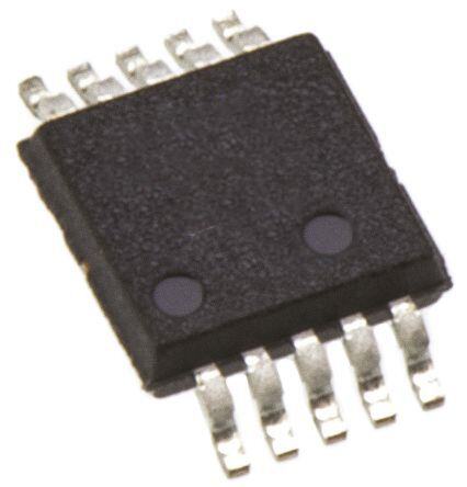
| 描述 | IC RHEOSTAT 5V 50-TP 256 10MSOP数字电位计 IC 256-pos 5v SPI 50-TP Mem Digi Rstat |
| 产品分类 | |
| 品牌 | Analog Devices |
| 产品手册 | |
| 产品图片 |
|
| rohs | 符合RoHS无铅 / 符合限制有害物质指令(RoHS)规范要求 |
| 产品系列 | 数字电位计 IC,Analog Devices AD5271BRMZ-100- |
| 数据手册 | |
| 产品型号 | AD5271BRMZ-100 |
| PCN设计/规格 | |
| POT数量 | Single |
| 产品种类 | 数字电位计 IC |
| 供应商器件封装 | 10-MSOP |
| 其它名称 | AD5271BRMZ100 |
| 包装 | 管件 |
| 商标 | Analog Devices |
| 存储器类型 | 非易失 |
| 安装类型 | 表面贴装 |
| 安装风格 | SMD/SMT |
| 容差 | 1 % |
| 封装 | Tube |
| 封装/外壳 | 10-TFSOP,10-MSOP(0.118",3.00mm 宽) |
| 封装/箱体 | MSOP-10 |
| 工作温度 | -40°C ~ 125°C |
| 工作电源电压 | 6 V |
| 工厂包装数量 | 50 |
| 弧刷存储器 | Non Volatile |
| 抽头 | 256 |
| 接口 | 4 线串行 |
| 数字接口 | SPI |
| 最大工作温度 | + 125 C |
| 最小工作温度 | - 40 C |
| 标准包装 | 50 |
| 每POT分接头 | 256 |
| 温度系数 | 5 PPM / C |
| 电压-电源 | 2.7 V ~ 5.5 V, ±2.5 V ~ 2.75 V |
| 电源电压-最大 | 5.5 V |
| 电源电压-最小 | 2.7 V |
| 电源电流 | 0.3 uA |
| 电路数 | 1 |
| 电阻 | 100 kOhms |
| 电阻(Ω) | 100k |
| 系列 | AD5271 |


- 商务部:美国ITC正式对集成电路等产品启动337调查
- 曝三星4nm工艺存在良率问题 高通将骁龙8 Gen1或转产台积电
- 太阳诱电将投资9.5亿元在常州建新厂生产MLCC 预计2023年完工
- 英特尔发布欧洲新工厂建设计划 深化IDM 2.0 战略
- 台积电先进制程称霸业界 有大客户加持明年业绩稳了
- 达到5530亿美元!SIA预计今年全球半导体销售额将创下新高
- 英特尔拟将自动驾驶子公司Mobileye上市 估值或超500亿美元
- 三星加码芯片和SET,合并消费电子和移动部门,撤换高东真等 CEO
- 三星电子宣布重大人事变动 还合并消费电子和移动部门
- 海关总署:前11个月进口集成电路产品价值2.52万亿元 增长14.8%


PDF Datasheet 数据手册内容提取
1024-/256-Position, 1% Resistor Tolerance Error, SPI Interface and 50-TP Memory Digital Rheostat Data Sheet AD5270/AD5271 FEATURES FUNCTIONAL BLOCK DIAGRAM Single-channel, 1024-/256-position resolution VDD 20 kΩ, 50 kΩ, 100 kΩ nominal resistance Maximum ±1% nominal resistor tolerance error POWER-ON 50-times programmable (50-TP) wiper memory RESET AD5270/AD5271 Rheostat mode temperature coefficient: 5 ppm/°C 2.7 V to 5.5 V single-supply operation ±2.5 V to ±2.75 V dual-supply operation for ac or bipolar RDAC SCLK REGISTER A operations 10/8 SERIAL SPI-compatible interface SYNC INTERFACE W Wiper setting readback DIN 50-TP Power on refreshed from 50-TP memory MEMORY BLOCK Thin LFCSP, 10-lead, 3 mm × 3 mm × 0.8 mm package SDO Compact MSOP, 10-lead, 3 mm × 4.9 mm × 1.1 mm package APPLICATIONS VSS EXT_CAP GND 08077-001 Mechanical rheostat replacements Figure 1. Op-amp: variable gain control Instrumentation: gain, offset adjustment Programmable voltage to current conversions Programmable filters, delays, time constants Programmable power supply Sensor calibration GENERAL DESCRIPTION The AD5270/AD5271 device wiper settings are controllable through the SPI digital interface. Unlimited adjustments are The AD5270/AD52711 are single-channel, 1024-/256-position allowed before programming the resistance value into the digital rheostats that combine industry leading variable resistor 50-TP memory. The AD5270/AD5271 do not require any performance with nonvolatile memory (NVM) in a compact external voltage supply to facilitate fuse blow and there are package. 50 opportunities for permanent programming. During 50-TP The AD5270/AD5271 ensure less than 1% end-to-end resistor activation, a permanent blow fuse command freezes the resistance tolerance error and offer 50-times programmable (50-TP) memory. position (analogous to placing epoxy on a mechanical trimmer). The guaranteed industry leading low resistor tolerance error The AD5270/AD5271 are available in a 3 mm × 3 mm, 10-lead feature simplifies open-loop applications as well as precision LFCSP package and in a 10-lead MSOP package. The parts are calibration and tolerance matching applications. guaranteed to operate over the extended industrial temperature range of −40°C to +125°C. 1 Protected by U.S.Patent Number 7688240 Rev. F Document Feedback Information furnished by Analog Devices is believed to be accurate and reliable. However, no responsibility is assumed by Analog Devices for its use, nor for any infringements of patents or other One Technology Way, P.O. Box 9106, Norwood, MA 02062-9106, U.S.A. rights of third parties that may result from its use. Specifications subject to change without notice. No license is granted by implication or otherwise under any patent or patent rights of Analog Devices. Tel: 781.329.4700 ©2009–2013 Analog Devices, Inc. All rights reserved. Trademarks and registered trademarks are the property of their respective owners. Technical Support www.analog.com
AD5270/AD5271 Data Sheet TABLE OF CONTENTS Features .............................................................................................. 1 Shift Register ............................................................................... 18 Applications ....................................................................................... 1 RDAC Register ............................................................................ 18 Functional Block Diagram .............................................................. 1 50-TP Memory Block ................................................................ 18 General Description ......................................................................... 1 Write Protection ......................................................................... 18 Revision History ............................................................................... 2 RDAC and 50-TP Read Operation .......................................... 19 Specifications ..................................................................................... 3 Shut-Down Mode ....................................................................... 20 Electrical Characteristics—AD5270 .......................................... 3 Resistor Performance Mode ...................................................... 20 Electrical Characteristics—AD5271 .......................................... 5 Reset ............................................................................................. 20 Interface Timing Specifications .................................................. 7 SDO Pin and Daisy-Chain Operation ..................................... 21 Absolute Maximum Ratings ............................................................ 9 RDAC Architecture .................................................................... 21 Thermal Resistance ...................................................................... 9 Programming the Variable Resistor ......................................... 22 ESD Caution .................................................................................. 9 EXT_CAP Capacitor .................................................................. 22 Pin Configuration and Function Descriptions ........................... 10 Terminal Voltage Operating Range ......................................... 22 Typical Performance Characteristics ........................................... 11 Power-Up Sequence ................................................................... 22 Test Circuits ..................................................................................... 17 Outline Dimensions ....................................................................... 23 Theory of Operation ...................................................................... 18 Ordering Guide .......................................................................... 24 Serial Data Interface ................................................................... 18 REVISION HISTORY 3/13—Rev. E to Rev. F Added LFCSP Throughout .............................................................. 1 Changed Resistor Noise Density, R = 20 kΩ from 50 nV/√Hz Changed OTP to 50-TP Throughout.............................................. 1 AW to 13 nV/√Hz; Table 1 ...................................................................... 4 Changes to Product Title, Features, and General Description .... 1 Changed Resistor Noise Density, R = 20 kΩ from 50 nV/√Hz Changes to Table 1 ............................................................................. 3 AW to 13 nV/√Hz; Table 4 ...................................................................... 6 Added Table 3; Renumbered Sequentially ..................................... 4 Updated Outline Dimensions ....................................................... 23 Changes to Table 4 ............................................................................. 5 Added Table 6 .................................................................................... 6 Changes to Table 8 and Table 9........................................................ 9 12/10—Rev. D to Rev. E Added Figure 6 and changes to Table 10 ..................................... 10 Changes to SDO Pin Description ................................................. 10 Replaced Typical Performance Characteristics Section ............ 11 Changes to SDO Pin and Daisy-Chain Operation Section ....... 21 Changes to Figure 44 ...................................................................... 21 Updated Outline Dimensions ....................................................... 23 11/10—Rev. C to Rev. D Changes to Ordering Guide .......................................................... 24 Changes to Figure 25 ...................................................................... 14 3/10—Rev. 0 to Rev. A 9/10—Rev. B to Rev. C Changes to Product Title and General Description.....................1 Changes to Figure 3 Caption ........................................................... 7 Changes to Figure 4 Caption ........................................................... 8 Changes to Theory of Operation Section...................................14 Deleted Daisy-Chain Operation Section, Added SDO Pin and 10/09—Revision 0: Initial Version Daisy-Chain Operation Section ................................................... 21 5/10—Rev. A to Rev. B Rev. F | Page 2 of 24
Data Sheet AD5270/AD5271 SPECIFICATIONS ELECTRICAL CHARACTERISTICS—AD5270 VDD = 2.7 V to 5.5 V, VSS = 0 V; VDD = 2.5 V to 2.75 V, VSS = −2.5 V to −2.75 V; −40°C < TA < +125°C, unless otherwise noted. Table 1. Parameter Symbol Test Conditions/Comments Min Typ1 Max Unit DC CHARACTERISTICS—RHEOSTAT MODE Resolution 10 Bits Resistor Integral Nonlinearity2, 3 R-INL R = 20 kΩ, |V − V | = 3.0 V to 5.5 V −1 +1 LSB AW DD SS R = 20 kΩ, |V − V | = 2.7 V to 3.0 V −1 +1.5 LSB AW DD SS R = 50 kΩ, 100 kΩ −1 +1 LSB AW Resistor Differential Nonlinearity2 R-DNL −1 +1 LSB Nominal Resistor Tolerance R-Perf Mode4 See Table 2 and Table 3 −1 ±0.5 +1 % Normal Mode ±15 % Resistance Temperature Coefficient5, 6 Code = full scale 5 ppm/°C Wiper Resistance Code = zero scale 35 70 Ω RESISTOR TERMINALS Terminal Voltage Range5, 7 VSS VDD V Capacitance5 A f = 1 MHz, measured to GND, code = 90 pF half scale Capacitance5 W f = 1 MHz, measured to GND, code = 40 pF half scale Common-Mode Leakage Current5 VA = VW 50 nA DIGITAL INPUTS Input Logic5 High V 2.0 V INH Low V 0.8 V INL Input Current I ±1 µA IN Input Capacitance5 CIN 5 pF DIGITAL OUTPUT Output Voltage5 High V R = 2.2 kΩ to V V − 0.1 V OH PULL_UP DD DD Low V R = 2.2 kΩ to V OL PULL_UP DD V = 2.7 V to 5.5 V, V = 0 V 0.4 V DD SS V = 2.5 V to 2.75 V, V = −2.5 V to −2.75 V 0.6 V DD SS Tristate Leakage Current −1 +1 µA Output Capacitance5 5 pF POWER SUPPLIES Single-Supply Power Range V = 0 V 2.7 5.5 V SS Dual-Supply Power Range ±2.5 ±2.75 V Supply Current Positive I 1 µA DD Negative I −1 µA SS 50-TP Store Current5, 8 Positive I 4 mA DD_OTP_STORE Negative I −4 mA SS_OTP_STORE OTP Read Current5, 9 Positive I 500 µA DD_OTP_READ Negative I −500 µA SS_OTP_READ Rev. F | Page 3 of 24
AD5270/AD5271 Data Sheet Parameter Symbol Test Conditions/Comments Min Typ1 Max Unit Power Dissipation10 V = V or V = GND 5.5 µW IH DD IL Power Supply Rejection Ratio5 PSRR ΔVDD/ΔVSS = ±5 V ± 10% dB R = 20 kΩ −66 −55 AW R = 50 kΩ −75 −67 AW R = 100 kΩ −78 −70 AW DYNAMIC CHARACTERISTICS5, 11 Bandwidth −3 dB, R = 10 kΩ, Terminal W, kHz AW see Figure 42 R = 20 kΩ 300 AW R = 50 kΩ 120 AW R = 100 kΩ 60 AW Total Harmonic Distortion V = 1 V rms, f = 1 kHz, dB A code = half scale R = 20 kΩ −90 AW R = 50 kΩ −88 AW R = 100 kΩ −85 AW Resistor Noise Density Code = half scale, T = 25°C nV/√Hz A R = 20 kΩ 13 AW R = 50 kΩ 25 AW R = 100 kΩ 32 AW 1 Typical specifications represent average readings at 25°C, VDD = 5 V, and VSS = 0 V. 2 Resistor position nonlinearity error (R-INL) is the deviation from an ideal value measured between the maximum resistance and the minimum resistance wiper positions. R-DNL measures the relative step change from ideal between successive tap positions. 3 The maximum current in each code is defined by IAW = (VDD − 1)/RAW. 4 The terms resistor performance mode and R-Perf mode are used interchangeably. See the Resistor Performance Mode section. 5 Guaranteed by design and not subject to production test. 6 See Figure 25 for more details. 7 Resistor Terminal A and Resistor Terminal W have no limitations on polarity with respect to each other. Dual-supply operation enables ground referenced bipolar signal adjustment. 8 Different from operating current, the supply current for the fuse program lasts approximately 55 ms. 9 Different from operating current, the supply current for the fuse read lasts approximately 500 ns. 10 PDISS is calculated from (IDD × VDD) + (ISS × VSS). 11 All dynamic characteristics use VDD = +2.5 V, VSS = −2.5 V. Table 2. AD5270—20 kΩ Resistor Performance Mode Code Range Resistor Tolerance Per Code |V − V | = 4.5 V to 5.5 V |V − V | = 2.7 V to 4.5 V DD SS DD SS R-TOLERANCE 1% R-Tolerance From 0x078 to 0x3FF From 0x0BE to 0x3FF 2% R-Tolerance From 0x037 to 0x3FF From 0x055 to 0x3FF 3% R-Tolerance From 0x028 to 0x3FF From 0x037 to 0x3FF Table 3. AD5270—50 kΩ and 100 kΩ Resistor Performance Mode Code Range Resistor Tolerance Per Code R = 50 kΩ R = 100 kΩ AW AW R-TOLERANCE 1% R-Tolerance From 0x078 to 0x3FF From 0x04B to 0x3FF 2% R-Tolerance From 0x055 to 0x3FF From 0x032 to 0x3FF 3% R-Tolerance From 0x032 to 0x3FF From 0x019 to 0x3FF Rev. F | Page 4 of 24
Data Sheet AD5270/AD5271 ELECTRICAL CHARACTERISTICS—AD5271 VDD = 2.7 V to 5.5 V, VSS = 0 V; VDD = 2.5 V to 2.75 V, VSS = −2.5 V to −2.75 V; −40°C < TA < +125°C, unless otherwise noted. Table 4. Parameter Symbol Test Conditions/Comments Min Typ1 Max Unit DC CHARACTERISTICS—RHEOSTAT MODE Resolution 8 Bits Resistor Integral Nonlinearity2, 3 R-INL −1 +1 LSB Resistor Differential Nonlinearity2 R-DNL −1 +1 LSB Nominal Resistor Tolerance R-Perf Mode4 See Table 5 and Table 6 −1 ±0.5 +1 % Normal Mode ±15 % Resistance Temperature Coefficient5, 6 Code = full scale 5 ppm/°C Wiper Resistance Code = zero scale 35 70 Ω RESISTOR TERMINALS Terminal Voltage Range5, 7 V V V SS DD Capacitance5 A f = 1 MHz, measured to GND, code = 90 pF half scale Capacitance5 W f = 1 MHz, measured to GND, code = 40 pF half scale Common-Mode Leakage Current5 V = V 50 nA A W DIGITAL INPUTS Input Logic5 High V 2.0 V INH Low5 V 0.8 V INL Input Current I ±1 µA IN Input Capacitance5 C 5 pF IN DIGITAL OUTPUT Output Voltage5 High V R = 2.2 kΩ to V V − 0.1 V OH PULL_UP DD DD Low V R = 2.2 kΩ to V OL PULL_UP DD V = 2.7 V to 5.5 V, V = 0 V 0.4 V DD SS V = 2.5 V to 2.75 V, V = −2.5 V to −2.75 V 0.6 V DD SS Tristate Leakage Current −1 +1 µA Output Capacitance5 5 pF POWER SUPPLIES Single-Supply Power Range V = 0 V 2.7 5.5 V SS Dual-Supply Power Range ±2.5 ±2.75 V Supply Current Positive I 1 µA DD Negative I −1 µA SS 50-TP Store Current5, 8 Positive I 4 mA DD_OTP_STORE Negative I −4 mA SS_OTP_STORE OTP Read Current5, 9 Positive I 500 µA DD_OTP_READ Negative I −500 µA SS_OTP_READ Power Dissipation10 V = V or V = GND 5.5 µW IH DD IL Power Supply Rejection Ratio5 PSRR ΔV /ΔV = ±5 V ± 10% dB DD SS R = 20 kΩ −66 −55 AW R = 50 kΩ −75 −67 AW R = 100 kΩ −78 −70 AW Rev. F | Page 5 of 24
AD5270/AD5271 Data Sheet Parameter Symbol Test Conditions/Comments Min Typ1 Max Unit DYNAMIC CHARACTERISTICS5, 11 Bandwidth −3 dB, R = 10 kΩ, Terminal W, see Figure 42 kHz AW R = 20 kΩ 300 AW R = 50 kΩ 120 AW R = 100 kΩ 60 AW Total Harmonic Distortion V = 1 V rms, f = 1 kHz, code = half scale dB A R = 20 kΩ −90 AW R = 50 kΩ −88 AW R = 100 kΩ −85 AW Resistor Noise Density Code = half scale, T = 25°C nV/√Hz A R = 20 kΩ 13 AW R = 50 kΩ 25 AW R = 100 kΩ 32 AW 1 Typical specifications represent average readings at 25°C, VDD = 5 V, and VSS = 0 V. 2 Resistor position nonlinearity error (R-INL) is the deviation from an ideal value measured between the maximum resistance and the minimum resistance wiper positions. R-DNL measures the relative step change from ideal between successive tap positions. 3 The maximum current in each code is defined by IAW = (VDD − 1)/RAW. 4 The terms resistor performance mode and R-Perf mode are used interchangeably. See the Resistor Performance Mode section. 5 Guaranteed by design and not subject to production test. 6 See Figure 25 for more details. 7 Resistor Terminal A and Resistor Terminal W have no limitations on polarity with respect to each other. Dual-supply operation enables ground referenced bipolar signal adjustment. 8 Different from operating current, the supply current for the fuse program lasts approximately 55 ms. 9 Different from operating current, the supply current for the fuse read lasts approximately 500 ns. 10 PDISS is calculated from (IDD × VDD) + (ISS × VSS). 11 All dynamic characteristics use VDD = +2.5 V, VSS = −2.5 V. Table 5. AD5271—20 kΩ Resistor Performance Mode Code Range Resistor Tolerance per Code |V − V | = 4.5 V to 5.5 V |V − V | = 2.7 V to 4.5 V DD SS DD SS R-TOLERANCE 1% R-Tolerance From 0x1E to 0xFF From 0x32 to 0xFF 2% R-Tolerance From 0x0F to 0xFF From 0x19 to 0xFF 3% R-Tolerance From 0x06 to 0xFF From 0x0E to 0xFF Table 6. AD5271—50 kΩ and 100 kΩ Resistor Performance Mode Code Range Resistor Tolerance per Code R = 50 kΩ R = 100 kΩ AW AW R-TOLERANCE 1% R-Tolerance From 0x1E to 0xFF From 0x14 to 0xFF 2% R-Tolerance From 0x14 to 0xFF From 0x0F to 0xFF 3% R-Tolerance From 0x0A to 0xFF From 0x0A to 0xFF Rev. F | Page 6 of 24
Data Sheet AD5270/AD5271 INTERFACE TIMING SPECIFICATIONS V = 2.5 V to 5.5 V, V = 0 V; V = 2.5 V, V = −2.5 V; all specifications T to T , unless otherwise noted. DD SS DD SS MIN MAX Table 7. Parameter Limit1 Unit Test Conditions/Comments t2 20 ns min SCLK cycle time 1 t 10 ns min SCLK high time 2 t 10 ns min SCLK low time 3 t 15 ns min SYNC to SCLK falling edge setup time 4 t 5 ns min Data setup time 5 t 5 ns min Data hold time 6 t 1 ns min SCLK falling edge to SYNC rising edge 7 t3, 4 500 ns min Minimum SYNC high time 8 t 15 ns min SYNC rising edge to next SCLK fall ignored 9 t 5 450 ns max SCLK rising edge to SDO valid 10 t 2 μs max RDAC register write command execute time RDAC_R-PERF t 600 ns max RDAC register write command execute time RDAC_NORMAL t 6 μs max Memory readback execute time MEMORY_READ t 350 ms max Memory program time MEMORY_PROGRAM t 0.6 ms max Reset 50-TP restore time RESET t 6 2 ms max Power-on 50-TP restore time POWER-UP 1 All input signals are specified with tr = tf = 1 ns/V (10% to 90% of VDD) and timed from a voltage level of (VIL + VIH)/2. 2 Maximum SCLK frequency is 50 MHz. 3 Refer to tRDAC_R-PER and tRDAC_NORMAL for RDAC register write operations. 4 Refer to tMEMORY_READ and tMEMORY_PROGRAM for memory commands operations. 5 RPULL_UP = 2.2 kΩ to VDD with a capacitance load of 168 pF. 6 Maximum time after VDD − VSS is equal to 2.5 V. Shift Register and Timing Diagrams DB9 (MSB) DB0 (LSB) 0 0 C3 C2 C1 C0 D9 D8 D7 D6 D5 D4 D3 D2 D1 D0 CONTROL BITS DATA BITS 08077-002 Figure 2. Shift Register Content t4 t2 t1 t7 SCLK t8 t3 t9 SYNC t5 t6 DIN 0 0 C3 C2 D7 D6 D5 D2 D1 D0 SDO 08077-003 Figure 3. Write Timing Diagram (CPOL = 0, CPHA = 1) Rev. F | Page 7 of 24
AD5270/AD5271 Data Sheet SCLK t9 SYNC DIN 0 0 C3 D0 D0 0 0 C3 D1 D0 t10 SDO X X C3 D1 D0 08077-004 Figure 4. Read Timing Diagram (CPOL = 0, CPHA = 1) Rev. F | Page 8 of 24
Data Sheet AD5270/AD5271 ABSOLUTE MAXIMUM RATINGS T = 25°C, unless otherwise noted. A Stresses above those listed under Absolute Maximum Ratings may cause permanent damage to the device. This is a stress Table 8. rating only and functional operation of the device at these or Parameter Rating any other conditions above those indicated in the operational V to GND –0.3 V to +7.0 V DD section of this specification is not implied. Exposure to absolute V to GND +0.3 V to −7.0 V SS maximum rating conditions for extended periods may affect V to V 7 V DD SS device reliability. V , V to GND V − 0.3 V, V + 0.3 V A W SS DD Digital Input and Output Voltage to GND −0.3 V to V + 0.3 V THERMAL RESISTANCE DD EXT_CAP to V 7 V SS θ is defined by JEDEC specification JESD-51 and the value is JA I , I A W dependent on the test board and test environment. Continuous R = 20 kΩ ±3 mA Table 9. Thermal Resistance AW RAW = 50 kΩ, 100 kΩ ±2 mA Package Type θJA1 θJC Unit Pulsed1 10-Lead LFCSP 50 3 °C/W Frequency > 10 kHz ±MCC2/d3 10-Lead MSOP 135 N/A °C/W Frequency ≤ 10 kHz ±MCC2/√d3 1 JEDEC 2S2P test board, still air (0 m/s air flow). Operating Temperature Range4 −40°C to +125°C Maximum Junction Temperature 150°C (TJ Maximum) ESD CAUTION Storage Temperature Range −65°C to +150°C Reflow Soldering Peak Temperature 260°C Time at Peak Temperature 20 sec to 40 sec Package Power Dissipation (TJ max − TA)/θJA 1 Maximum terminal current is bounded by the maximum current handling of the switches, maximum power dissipation of the package, and maximum applied voltage across any two of the A and W terminals at a given resistance. 2 Maximum continuous current. 3 Pulse duty factor. 4 Includes programming of 50-TP memory. Rev. F | Page 9 of 24
AD5270/AD5271 Data Sheet PIN CONFIGURATION AND FUNCTION DESCRIPTIONS VDD 1 10SYNC A 2 AD5270/ 9 SCLK W 3 AD5271 8 DIN VDD 11 10 SYNC VSS 4 (EXPPAODS)ED 7 SDO A 22 AD5270/ 9 SCLK EXT_CAP 5 6 GND AD5271 W 33 8 DIN EXT_CVASPS 445 (NToOt Pto VSIEcaWle) 76 GSDNOD 08077-005 N1 . O TOTHREE SI SE XTPIEODS ETOD PVSASD. IS LEFT FLOATING 08077-040 Figure 5. MSOP Pin Configuration Figure 6. LFCSP Pin Configuration Table 10. Pin Function Descriptions Pin No. Mnemonic Description 1 V Positive Power Supply. Decouple this pin with 0.1 μF ceramic capacitors and 10 μF capacitors. DD 2 A Terminal A of RDAC. V ≤ V ≤ V . SS A DD 3 W Wiper Terminal of RDAC. V ≤ V ≤ V . SS W DD 4 V Negative Supply. Connect to 0 V for single-supply applications. Decouple this pin with 0.1 μF ceramic SS capacitors and 10 μF capacitors. 5 EXT_CAP External Capacitor. Connect a 1 μF capacitor between EXT_CAP and V . This capacitor must have a voltage SS rating of ≥7 V. 6 GND Ground Pin, Logic Ground Reference. 7 SDO Serial Data Output. This pin can be used to clock data from the shift register in daisy-chain mode or in readback mode. This open-drain output requires an external pull-up resistor even if it is not use. 8 DIN Serial Data Line. This pin is used in conjunction with the SCLK line to clock data into or out of the 16-bit input register. 9 SCLK Serial Clock Input. Data is clocked into the shift register on the falling edge of the serial clock input. Data can be transferred at rates up to 50 MHz. 10 SYNC Falling Edge Synchronization Signal. This is the frame synchronization signal for the input data. When SYNC goes low, it enables the shift register and data is transferred in on the falling edges of the subsequent clocks. The selected register is updated on the rising edge of SYNC following the 16th clock cycle. If SYNC is taken high before the 16th clock cycle, the rising edge of SYNC acts as an interrupt, and the write sequence is ignored by the RDAC. EPAD Exposed Pad Leave floating or connected to V . SS Rev. F | Page 10 of 24
Data Sheet AD5270/AD5271 TYPICAL PERFORMANCE CHARACTERISTICS 0.8 0.8 ++12255°C°C RAW = 20kΩ TA = 25°C 20kΩ 0.6 –40°C 0.6 5100k0ΩkΩ 0.4 0.4 B) B) S S NL (L 0.2 NL (L0.2 I I 0 0 –0.2 –0.2 –0.40 128 256 38C4ODE 5(D12ecima6l)40 768 896 1023 08077-010 –0.40 256 CODE 5(1D2ecimal) 768 1023 08077-111 Figure 7. R-INL in R-Perf Mode vs. Code vs. Temperature (AD5270) Figure 10. R-INL in R-Perf Mode vs. Code vs. Nominal Resistance (AD5270) 0.2 0.6 RAW = 20kΩ TA = 25°C 0.1 0.4 0 0.2 –0.1 B) B) S S L (L –0.2 L (L 0 N N D D –0.3 –0.2 –0.4 –0.4 –0.5 –40°C +25°C +125°C 20kΩ 50kΩ 100kΩ –0.60 128 256 38C4ODE 5(1D2ecima6l4)0 768 896 1023 08077-011 –0.60 256 CODE5 (1D2ecimal) 768 1023 08077-120 Figure 8. R-DNL in R-Perf Mode vs. Code vs. Temperature (AD5270) Figure 11. R-DNL in R-Perf Mode vs. Code vs. Nominal Resistance (AD5270) 0.50 0.6 ++12255°C°C RAW = 20kΩ TA = 25°C 2500kkΩΩ –40°C 100kΩ 0.40 0.4 0.30 0.2 B) B) NL (LS 0.20 NL (LS I I 0 0.10 –0.2 0 –0.100 128 256 38C4ODE 5(D1e2cima6l)40 768 896 1023 08077-014 –0.40 256 CODE 5(1D2ecimal) 768 1023 08077-121 Figure 9. R-INL in Normal Mode vs. Code vs. Temperature (AD5270) Figure 12. R-INL in Normal Mode vs. Code vs. Nominal Resistance (AD5270) Rev. F | Page 11 of 24
AD5270/AD5271 Data Sheet 0.15 0.15 ++12255°C°C RAW = 20kΩ TA = 25°C 20kΩ 50kΩ 0.10 –40°C 0.10 100kΩ 0.05 0.05 B) B) 0 S S L (L 0 L (L DN DN–0.05 –0.05 –0.10 –0.10 –0.15 –0.150 128 256 38C4ODE 5(D1e2cima6l)40 768 896 1023 08077-015 –0.200 256 CODE5 (1D2ecimal) 768 1023 08077-122 Figure 13. R-DNL in Normal Mode vs. Code vs. Temperature (AD5270) Figure 16. R-DNL in Normal Mode vs. Code vs. Nominal Resistance (AD5270) 0.20 0.15 ++12255°C°C RAW = 20kΩ TA = 25°C 2100k0ΩkΩ –40°C 0.15 0.10 0.10 B) B) 0.05 S S NL (L 0.05 NL (L I I 0 0 –0.05 –0.05 –0.100 64 CODE 1(D28ecimal) 192 255 08077-013 –0.100 64 CODE 1(D28ecimal) 192 255 08077-123 Figure 14. R-INL in R-Perf Mode vs. Code vs. Temperature (AD5271) Figure 17. R-INL in R-Perf Mode vs. Code vs. Nominal Resistance (AD5271) 0.06 0.15 0.04 RAW = 20kΩ ++12255°C°C TA = 25°C –40°C 0.10 0.02 0 0.05 B) –0.02 B) S S L (L –0.04 L (L 0 N N D –0.06 D –0.05 –0.08 –0.10 –0.10 –0.12 20kΩ 100kΩ –0.140 64 CODE 1(D28ecimal) 192 255 08077-012 –0.150 64 CODE 1(D28ecimal) 192 255 08077-125 Figure 15. R-DNL in R-Perf Mode vs. Code vs. Temperature (AD5271) Figure 18. R-DNL in R-Perf Mode vs. Code vs. Nominal Resistance (AD5271) Rev. F | Page 12 of 24
Data Sheet AD5270/AD5271 0.10 0.15 ++12255°C°C RAW = 20kΩ TA = 25°C 2100k0ΩkΩ –40°C 0.08 0.10 0.06 B) B) 0.05 S S NL (L 0.04 NL (L I I 0 0.02 –0.05 0 –0.020 64 CODE 1(D28ecimal) 192 255 08077-016 –0.100 64 CODE 1(D28ecimal) 192 255 08077-126 Figure 19. R-INL in Normal Mode vs. Code vs. Temperature (AD5271) Figure 22. R-INL in Normal Mode vs. Code vs. Nominal Resistance (AD5271) 0.03 0.010 RAW = 20kΩ +125°C 100kΩ TA = 25°C +25°C 20kΩ –40°C 0.02 0.008 0.01 0.006 DNL (LSB) 0 DNL (LSB) 0.004 –0.01 0.002 –0.02 0 –0.030 64 CODE 1(D28ecimal) 192 255 08077-017 –0.0020 64 CODE 1(D28ecimal) 192 255 08077-027 Figure 20. R-DNL in Normal Mode vs. Code vs. Temperature (AD5271) Figure 23. R-DNL in Normal Mode vs. Code vs. Nominal Resistance (AD5271) 500 1.0 400 IDD = 5V 300 0.8 200 nA) 100 IDD = 3V mA) 0.6 T ( T ( EN 0 ISS = 3V EN R R UR –100 UR 0.4 C C –200 ISS = 5V –300 0.2 –400 0 –50–040 –30–20–10 0 10TEM20PE3R0AT4U0RE5 (0°C)60 70 80 90 100110 08077-018 0 0.5 1.0 1.5 2.0VO2.L5TAG3.E0 (V)3.5 4.0 4.5 5.0 5.5 08077-023 Figure 21. Supply Current (IDD, ISS) vs. Temperature Figure 24. Supply Current IDD vs. Digital Input Voltage Rev. F | Page 13 of 24
AD5270/AD5271 Data Sheet 50 7 VDD/VSS= 5V/0V VDD/VSS=5V/0V 45 C) 20kΩ 6 20kΩ pm/° 40 5100k0ΩkΩ A) 5100k0ΩkΩ CO (p 35 (mAX 5 P 30 M E TEM 25 L IWA_ 4 D A MO 20 TIC 3 STAT 15 EORE 2 O H E 10 T H R 1 5 0 0 00 26546 CODE 15(D2182ecimal) 179628 1205253 AADD55227701 08077-019 00 26546 CODE 15(21D82ecimal) 179628 1205253 AADD55227710 08077-028 Figure 25. Tempco ΔRWA/ΔT vs. Code Figure 28. Theoretical Maximum Current vs. Code 0 0 0x200 (0x80) AD5270 (AD5271) 0x200 (0x80) AD5270 (AD5271) –10 0x100 (0x40) –10 0x100 (0x40) 0x080 (0x20) 0x080 (0x20) –20 0x040 (0x10) –20 0x040 (0x10) 0x020 (0x08) B) B)–30 N (d –30 0x020 (0x08) N (d 0x010 (0x04) GAI 0x010 (0x04) GAI–40 0x008 (0x02) 0x008 (0x02) 0x004 (0x01) –40 0x004 (0x01) –50 0x002 0x002 0x001 –50 –60 0x001 –60 –70 1k 10k FREQU1E0N0kCY (Hz) 1M 10M 08077-031 1k 10k FREQU1E0N0kCY (Hz) 1M 10M 08077-041 Figure 26. 20 kΩ Gain vs. Code vs. Frequency Figure 29. 100 kΩ Gain vs. Code vs. Frequency 0 0 0x200 (0x80) AD5270 (AD5271) VCDODD /EV S=S H=A 5LVF/0 SVCALE –10 –10 0x100 (0x40) 50kΩ –20 100kΩ 0x080 (0x20) 20kΩ –20 –30 0x040 (0x10) N (dB)–30 0x020 (0x08) R (dB)–40 GAI 0x010 (0x04) PSR–50 –40 0x008 (0x02) –60 0x004 (0x01) –70 –50 0x002 0x001 –80 –601k 10k FREQU1E0N0kCY (Hz) 1M 10M 08077-032 –90100 1k FREQUENCY (Hz)10k 100k 08077-024 Figure 27. 50 kΩ Gain vs. Code vs. Frequency Figure 30. PSRR vs. Frequency Rev. F | Page 14 of 24
Data Sheet AD5270/AD5271 0 0 VDD/VSS= 5V/0V 20kΩ VDD/VSS = 5V/0V CODE = HALF SCALE 50kΩ –10 CODE = HALF SCALE NOISE BW = 22kHz 100kΩ fIN= 1kHz –20 VIN= 1V rms –20 NOISE BW = 22kHz –30 20kΩ B) 50kΩ N (dB)–40 + N (d–40 100kΩ + D –50 THD –60 TH–60 –70 –80 –80 –90 –100100 1k FREQUENCY (H1z0)k 100k 08077-025 –1000.001 0.01VOLTAGE (VRMS0).1 1 08077-026 Figure 31. THD + N vs. Frequency Figure 34. THD + N vs. Amplitude 0.03 0.0010 20kΩ VDD/VSS = 5V/0V 50kΩ IAW = 200µA 0.02 100kΩ CODE = HALF SCALE 0.0005 0.01 GE (V) 0 E (V) 0 A G T A OL–0.01 LT V O–0.0005 V –0.02 –0.0010 –0.03 –0.04–1 4 T9IME (µs) 14 19 08077-043 –0.0015–10 0 10 2T0IME (µs3)0 40 50 60 08077-046 Figure 32. Maximum Glitch Energy Figure 35. Digital Feedthrough 45 11.25 70 15.5 TA = 25°C VDD/VSS= 5V/0V 40 20kΩ 10.00 20kΩ 50kΩ 60 50kΩ 15.0 AD5270) 3350 100kΩ 78..5705 AD5271) D5270) 50 100kΩ 12.5 D5271) DES ( 25 6.25 DES ( ES (A 40 10.0 ES (A O O D D C C O O OF 20 5.00 OF F C 30 7.5 F C MBER 15 3.75 MBER BER O 20 5.0 BER O NU 10 2.50 NU UM UM N N 10 2.5 5 1.25 02.7 3.2 3.7 VDD 4(V.2) 4.7 5.2 0 08077-021 –040 –20 0 T2E0MPER4A0TURE6 (0°C) 80 100 120 0 08077-020 Figure 33. Maximum Code Loss vs. Voltage Figure 36. Maximum Code Loss vs. Temperature Rev. F | Page 15 of 24
AD5270/AD5271 Data Sheet 8 0.006 VDD/VSS = 5V/0V IAW = 10µA 0.005 CODE = HALF SCALE 7 %)0.004 E ( OLTAGE (V) 6 RESISTANC00..000023 V W0.001 A R Δ 5 0 –0.001 40.07 0.09 0T.1I1ME (Secon0d.1s3) 0.15 0.17 08077-029 –0.0020 100 200 O3P0E0RA4T0IO0N A50T0 1506°C00 (Ho7u0r0s) 800 900 1000 08077-038 Figure 37. VEXT_CAP Waveform While Writing Fuse Figure 38. Long-Term Drift Accelerated Average by Burn-In Rev. F | Page 16 of 24
Data Sheet AD5270/AD5271 TEST CIRCUITS Figure 39 to Figure 43 define the test conditions used in the Specifications section. DUT DUT IW W W 1GΩ A A V VMS 08077-033 VMS 08077-036 Figure 39. Resistor Position Nonlinearity Error Figure 42. Gain vs. Frequency (Rheostat Operation; R-INL, R-DNL) VMS DUT GND RWA = IW ICM W +2.75V DUT CODE = 0x00 IW RW =RW2A A –2.75V W GND A VMS 08077-034 N+C2.75V –2.7G5VND NC = NO CONNECT 08077-037 Figure 40. Wiper Resistance Figure 43. Common Leakage Current V+ = VDD ±10% PSRR (dB) = 20 LOG VMS VDD VDD W IW PSS (%/%) =ΔΔVVMDDS%% V+ A VMS 08077-035 Figure 41. Power Supply Sensitivity (PSS, PSRR) Rev. F | Page 17 of 24
AD5270/AD5271 Data Sheet THEORY OF OPERATION The AD5270 and AD5271 are designed to operate as true RDAC REGISTER variable resistors for analog signals within the terminal voltage The RDAC register directly controls the position of the digital range of V < V < V . The RDAC register contents deter- SS TERM DD rheostat wiper. For example, when the RDAC register is loaded mine the resistor wiper position. The RDAC register acts as a with all zeros, the wiper is connected to Terminal A of the variable scratchpad register, which allows unlimited changes of resistance resistor. The RDAC register is a standard logic register and settings. The RDAC register can be programmed with any position there is no restriction on the number of changes allowed. The setting using the SPI interface. When a desirable wiper position basic mode of setting the variable resistor wiper position is found, this value can be stored in a 50-TP memory register. (programming the RDAC register) is accomplished by loading Thereafter, the wiper position is always restored to that position the serial data input register with Command 1 (see Table 11) and for subsequent power-up. The storing of 50-TP data takes approx- with the desired wiper position data. imately 350 ms; during this time, the AD5270/AD5271 lock to 50-TP MEMORY BLOCK prevent any changes from taking place. The AD5270/AD5271 contain an array of 50-TP programmable The AD5270/AD5271 also feature a patented 1% end-to-end memory registers, which allow the wiper position to be pro- resistor tolerance. This simplifies precision, rheostat mode, and grammed up to 50 times. Table 13 shows the memory map. open-loop applications where knowledge of absolute resistance When the desired wiper position is determined, the user can is critical. load the serial data input register with Command 3 (see Table 11) SERIAL DATA INTERFACE which stores the wiper position data in a 50-TP memory register. The first address to be programmed is Location 0x01 The AD5270/AD5271 contain a serial interface (SYNC, SCLK, (see Table 13); the AD5270/AD5271 increments the 50-TP DIN , and SDO), which is compatible with SPI interface standards, memory address for each subsequent program until the memory as well as most DSPs. This device allows writing of data via the is full. Programming data to 50-TP consumes approximately serial interface to every register. 4 mA for 55 ms, and takes approximately 350 ms to complete, SHIFT REGISTER during which time the shift register locks to prevent any changes For the AD5270/AD5271, the shift register is 16 bits wide, as from occurring. Bit C3 of the control register can be polled to shown in Figure 2. The 16-bit word consists of two unused bits, verify that the fuse program command was completed properly. which should be set to zero, followed by four control bits and No change in supply voltage is required to program the 50-TP 10 RDAC data bits (note that for the AD5271 only, the lower memory; however, a 1 μF capacitor on the EXT_CAP pin is two RDAC data bits are don’t care if the RDAC register is read required (see Figure 46). Prior to 50-TP activation, the AD5270 from or written to). Data is loaded MSB first (Bit 15). The four and the AD5271 preset to midscale on power up. control bits determine the function of the software command as WRITE PROTECTION listed in Table 11. Figure 3 shows a timing diagram of a typical At power-up, the serial data input register write commands for AD5270/AD5271 write sequence. both the RDAC register and the 50-TP memory registers are The write sequence begins by bringing the SYNC line low. The disabled. The RDAC write protect bit, C1, of the control register SYNC pin must be held low until the complete data-word is (see Table 13 and Table 14) is set to 0 by default. This disables loaded from the DIN pin. When SYNC returns high, the serial any change of the RDAC register content regardless of the data-word is decoded according to the instructions in Table 11. software commands, except that the RDAC register can be The command bits (Cx) control the operation of the digital refreshed from the 50-TP memory using the software reset, potentiometer. The data bits (Dx) are the values that are loaded Command 4. To enable programming of the RDAC register, the into the decoded register. The AD5270/AD5271 have an internal write protect bit (Bit C1), of the control register must first be counter that counts a multiple of 16 bits (a frame) for proper programmed by loading the serial data input register with operation. For example, AD5270/AD5271 each works with a Command 7. To enable programming of the 50-TP memory, 32-bit word but do not work properly with a 31-bit or 33-bit the program enable bit (Bit C0) of the control register, which is word. The AD5270/AD5271 do not require a continuous SCLK set to 0 by default, must first be set to 1. when SYNC is high. To minimize power consumption in the digital input buffers, operate all serial interface pins close to the V supply rails. DD Rev. F | Page 18 of 24
Data Sheet AD5270/AD5271 RDAC AND 50-TP READ OPERATION Data from the selected memory location is clocked out of the SDO pin during the next SPI operation. A binary encoded A serial data output SDO pin is available for readback of the version address of the most recently programmed wiper memory internal RDAC register or 50-TP memory contents. The location can be read back using Command 6 (see Table 11). This contents of the RDAC register can be read back through SDO can be used to monitor the spare memory status of the 50-TP by using Command 2 (see Table 11). Data from the RDAC memory block. register is clocked out of the SDO pin during the last 10 clocks of the next SPI operation. Table 12 provides a sample listing for the sequence of serial data input (DIN) words with the serial data output appearing at the It is possible to read back the contents of any of the 50-TP SDO pin in hexadecimal format for a write and read to both the memory registers through SDO by using Command 5. The RDAC register and the 50-TP memory (Memory Location 20). lower six LSB bits, D0 to D5 of the data byte, select which memory location is to be read back, as shown in Table 13. Table 11. Command Operation Truth Table Command Command[DB13:DB10] Data[DB9:DB0]1 Number C3 C2 C1 C0 D9 D8 D7 D6 D5 D4 D3 D2 D1 D0 Operation 0 0 0 0 0 X X X X X X X X X X NOP: do nothing. 1 0 0 0 1 D9 D8 D7 D6 D5 D4 D3 D2 D12 D02 Write contents of serial register data to RDAC. 2 0 0 1 0 X X X X X X X X X X Read contents of RDAC wiper register. 3 0 0 1 1 X X X X X X X X X X Store wiper setting: store RDAC setting to 50-TP. 4 0 1 0 0 X X X X X X X X X X Software reset: refresh RDAC with last 50-TP memory stored value. 53 0 1 0 1 X X X X D5 D4 D3 D2 D1 D0 Read contents of 50-TP from SDO output in the next frame. 6 0 1 1 0 X X X X X X X X X X Read address of last 50-TP programmed memory location. 74 0 1 1 1 X X X X X X X D2 D1 D0 Write contents of serial register data to control register. 8 1 0 0 0 X X X X X X X X X X Read contents of control register. 9 1 0 0 1 X X X X X X X X X D0 Software shutdown. D0 = 0; normal mode. D0 = 1; device placed in shutdown mode. 1 X is don’t care. 2 AD5271 = don’t care. 3 See Table 15 for 50-TP memory map. 4 See Table 14 for bit details. Rev. F | Page 19 of 24
AD5270/AD5271 Data Sheet SHUT-DOWN MODE RESISTOR PERFORMANCE MODE The AD5270/AD5271 can be shut down by executing the This mode activates a new, patented 1% end-to-end resistor software shutdown command, Command 9 (see Table 11), and tolerance that ensures a ±1% resistor tolerance error on each setting the LSB to 1. This feature places the RDAC in a zero- code, that is, code = half scale, R = 10 kΩ ± 100 Ω. See Table 2, WA power-consumption state where Terminal Ax is open circuited Table 3, Table 5, and Table 6 to verify which codes achieve ±1% and the Wiper Terminal Wx remains connected. It is possible to resistor tolerance. The resistor performance mode is activated by execute any command from Table 11 while the AD5270/AD5271 programming Bit C2 of the control register. are in shutdown mode. The parts can be taken out of shutdown RESET mode by executing Command 9 and setting the LSB to 0 or by a The AD5270/AD5271 can be reset through software by executing software reset, Command 4 (see Table 11). Command 4 (see Table 11). The reset command loads the RDAC register with the contents of the most recently programmed 50-TP memory location. The RDAC register loads with midscale if no 50-TP memory location has been previously programmed. Table 12. Write and Read to RDAC and 50-TP Memory DIN SDO1 Action 0x1C03 0xXXXX Enable update of the wiper position and the 50-TP memory contents through the digital interface. 0x0500 0x1C03 Write 0x100 to the RDAC register; wiper moves to ¼ full-scale position. 0x0800 0x0500 Prepares data read from RDAC register. 0x0C00 0x100 Stores RDAC register content into the 50-TP memory. A 16-bit word appears out of SDO, where the last 10-bits contain the contents of the RDAC register (0x100). 0x1800 0x0C00 Prepares data read of last programmed 50-TP memory monitor location. 0x0000 0xXX19 NOP Instruction 0 sends a 16-bit word out of SDO, where the six LSBs last six bits contain the binary address of the last programmed 50-TP memory location, for example, 0x19 (see Table 13). 0x1419 0x0000 Prepares data read from Memory Location 0x19. 0x2000 0x0100 Prepares data read from the control register. Sends a 16-bit word out of SDO, where the last 10-bits contain the contents of Memory Location 0x19. 0x0000 0xXXXX NOP Instruction 0 sends a 16-bit word out of SDO, where the last four bits contain the contents of the control register. If Bit C3 = 1, the fuse program command successful. 1 X is don’t care. Table 13. Control Register Bit Map DB9 DB8 DB7 DB6 DB5 DB4 DB3 DB2 DB1 DB0 0 0 0 0 0 0 C3 C2 C1 C0 Table 14. Control Register Bit Description Bit Name Description C0 50-TP program enable 0 = 50-TP program disabled (default) 1 = enable device for 50-TP program C1 RDAC register write protect 0 = wiper position frozen to value in 50-TP memory (default)1 1 = allow update of wiper position through digital interface C2 R-performance enable 0 = RDAC resistor tolerance calibration enabled (default) 1 = RDAC resistor tolerance calibration disabled C3 50-TP memory program success bit 0 = fuse program command unsuccessful (default) 1 = fuse program command successful 1 Wiper position frozen to the last value programmed in the 50-TP memory. The wiper is frozen to midscale if the 50-TP memory has not been previously programmed. Rev. F | Page 20 of 24
Data Sheet AD5270/AD5271 Table 15. Memory Map Data Byte[DB9:DB8]1 Command Number D9 D8 D7 D6 D5 D4 D3 D2 D1 D0 Register Contents 5 X X X 0 0 0 0 0 0 0 Reserved X X X 0 0 0 0 0 0 1 1st programmed wiper location (0x01) X X X 0 0 0 0 0 1 0 2nd programmed wiper location (0x02) X X X 0 0 0 0 0 1 1 3rd programmed wiper location (0x03) X X X 0 0 0 0 1 0 0 4th programmed wiper location (0x04) … … … … … … … … … … … X X X 0 0 0 1 0 1 0 10th programmed wiper location (0xA) X X X 0 0 1 0 1 0 0 20th programmed wiper location (0x14) X X X 0 0 1 1 1 1 0 30th programmed wiper location (0x1E) X X X 0 1 0 1 0 0 0 40th programmed wiper location (0x28) X X X 0 1 1 0 0 1 0 50th programmed wiper location (0x32) 1 X is don’t care. VDD SDO PIN AND DAISY-CHAIN OPERATION The serial data output pin (SDO) serves two purposes: it can be AD5270/ RP AD5270/ AD5271 2.2kΩ AD5271 used to read the contents of the wiper setting and 50-TP values MOSI DIN U1SDO DIN U2SDO using Command 2 and Command 5, respectively (see Table 11), µC SCLK SS or the SDO pin can be used in daisy-chain mode. Data is clocked SYNC SCLK SYNC SCLK out of SDO on the rising edge of SCLK. The SDO pin contains aTno opplaecne- tdhrea ipni nN i-nc hhainghn eilm FpEeTd athnacte raenqdu imreisn ai- pmuilzle-u tph er epsoiswtoerr. 08077-006 Figure 44. Daisy-Chain Configuration Using SDO dissipation when the pin is used, the 0x8001 data word followed by Command 0 should be sent to the part. Table 16 provides a RDAC ARCHITECTURE sample listing for the sequence of the serial data input (DIN). To achieve optimum performance, Analog Devices has patented Daisy chaining minimizes the number of port pins required the RDAC segmentation architecture for all the digital potentio- from the controlling IC. As shown in Figure 44, the user must meters. In particular, the AD5270/AD5271 employ a three-stage tie the SDO pin of one package to the DIN pin of the next segmentation approach as shown in Figure 45.The AD5270/ package. The user may need to increase the clock period because AD5271 wiper switch is designed with the transmission gate the pull-up resistor and the capacitive loading at the SDO-to- CMOS topology. DIN interface may require additional time delay between subsequent devices. When two AD5270/AD5271 devices are A daisy-chained, 32 bits of data are required. The first 16 bits go to U2, and the second 16 bits go to U1. RL Table 16. Minimize Power Dissipation at the SDO Pin DIN SDO1 Action RL RM 0xXXXX 0xXXXX Last user command sent to the digipot. 0x8001 0xXXXX Prepares the SDO pin to be placed in 8-/10-BIT RM SW high impedance mode. DAEDCDORDESESR RW 0x0000 High The SDO pin is placed in high W Impedance impedance. RW 1K Xe iesp d othn’et cSaYreN. C pin low until all 32 bits are clocked to their 08077-007 Figure 45. Simplified RDAC Circuit respective serial registers. The SYNC pin is then pulled high to complete the operation. Rev. F | Page 21 of 24
AD5270/AD5271 Data Sheet PROGRAMMING THE VARIABLE RESISTOR TERMINAL VOLTAGE OPERATING RANGE Rheostat Operation—1% Resistor Tolerance The positive V and negative V power supplies of the DD SS The nominal resistance between Terminal W and Terminal A, RWA, AD5270/AD5271 define the boundary conditions for proper is 20 kΩ, 50 kΩ, or 100 kΩ and has 1024-/256-tap points accessed 2-terminal digital resistor operation. Supply signals present on by the wiper terminal. The 10-/8-bit data in the RDAC latch is Terminal A and Terminal W that exceed V or V are clamped DD SS decoded to select one of the 1024 or 256 possible wiper settings. by the internal forward-biased diodes, see Figure 47. The AD5270 and AD5271 contain an internal ±1% resistor VDD tolerance calibration feature that can be disabled or enabled, enabled by default, or by programming Bit C2 of the control register (see Table 13 and Table 14). A The digitally programmed output resistance between the W W terminal and the A terminal, R , is calibrated to give a WA maximum of ±1% absolute resistance error over both the full supply and temperature ranges. As a result, the general equations for determining the digitally programmed output rfoeslliostwainncge: between the W terminal and the A terminal are the VSS 08077-009 Figure 47. Maximum Terminal Voltages Set by VDD and VSS For the AD5270 The ground pins of the AD5270/AD5271 devices are primarily D R (D) R (1) used as digital ground references. To minimize the digital ground WA 1024 WA bounce, join the AD5270/AD5271 ground terminal remotely For the AD5271 to the common ground. The digital input control signals to the D AD5270/AD5271 must be referenced to the device ground pin R (D) R (2) WA 256 WA (GND), and must satisfy the logic level defined in the Specifications section. An internal level shift circuit ensures that where: the common-mode voltage range of the three terminals extends D is the decimal equivalent of the binary code loaded in the from V to V , regardless of the digital input level. 10-/8-bit RDAC register. SS DD R is the end-to-end resistance. POWER-UP SEQUENCE WA In the zero-scale condition, a finite total wiper resistance of Because there are diodes to limit the voltage compliance at 120 Ω is present. Regardless of which setting the part is oper- Terminal A and Terminal W (see Figure 47), it is important to ating in, take care to limit the current between Terminal A to power VDD/VSS first before applying any voltage to Terminal A Terminal W to the maximum continuous current of ±3 mA or and Terminal W; otherwise, the diode is forward-biased such a pulse current specified in Table 8. Otherwise, degradation or that V /V are powered unintentionally. The ideal power-up DD SS possible destruction of the internal switch contact can occur. sequence is V , GND, V , digital inputs, V , and V . The SS DD A W order of powering V , V , and the digital inputs is not EXT_CAP CAPACITOR A W important as long as they are powered after V /V . DD SS A 1 μF capacitor to V must be connected to the EXT_CAP SS As soon as V is powered, the power-on preset activates which pin, as shown in Figure 46, on power-up and throughout the DD first sets the RDAC to midscale and then restores the last pro- operation of the AD5270/AD5271. grammed 50-TP value to the RDAC register. AD5270/ AD5271 50_OTP EXT_CAP MEMORY C1 BLOCK 1µF VSS VSS 08077-008 Figure 46. EXT_CAP Hardware Setup Rev. F | Page 22 of 24
Data Sheet AD5270/AD5271 OUTLINE DIMENSIONS 3.10 3.00 2.90 10 6 5.15 3.10 4.90 3.00 4.65 2.90 1 5 PIN1 IDENTIFIER 0.50BSC 0.95 15°MAX 0.85 1.10MAX 0.75 0.70 0.15 0.30 6° 0.23 0.55 CO0P.0L5ANARITY 0.15 0° 0.13 0.40 0.10 COMPLIANTTOJEDECSTANDARDSMO-187-BA 091709-A Figure 48. 10-Lead Mini Small Outline Package [MSOP] (RM-10) Dimensions shown in millimeters 2.48 2.38 3.10 2.23 3.00 SQ 2.90 0.50 BSC 6 10 PIN 1 INDEX EXPOSED 1.74 AREA PAD 1.64 0.50 1.49 0.40 0.30 0.20 MIN 5 1 TOP VIEW BOTTOM VIEW PIN 1 INDICATOR (R 0.15) 0.80 FOR PROPER CONNECTION OF 0.75 0.05 MAX THE EXPOSED PAD, REFER TO THE PIN CONFIGURATION AND 0.70 0.02 NOM FUNCTION DESCRIPTIONS COPLANARITY SECTION OF THIS DATA SHEET. SEPALTAINNGE 000...322050 0.20 REF 0.08 02-05-2013-C Figure 49. 10-Lead Frame Chip Scale Package [LFCSP_WD] 3 mm × 3 mm Body, Very Thin, Dual Lead (CP-10-9) Dimensions shown in millimeters Rev. F | Page 23 of 24
AD5270/AD5271 Data Sheet ORDERING GUIDE Model1 R (kΩ) Resolution Temperature Range Package Description Package Option Branding AW AD5270BRMZ-20 20 1,024 −40°C to +125°C 10-Lead MSOP RM-10 D1X AD5270BRMZ-20-RL7 20 1,024 −40°C to +125°C 10-Lead MSOP RM-10 D1X AD5270BRMZ-50 50 1,024 −40°C to +125°C 10-Lead MSOP RM-10 DDP AD5270BRMZ-50-RL7 50 1,024 −40°C to +125°C 10-Lead MSOP RM-10 DDP AD5270BRMZ-100 100 1,024 −40°C to +125°C 10-Lead MSOP RM-10 D1W AD5270BRMZ-100-RL7 100 1,024 −40°C to +125°C 10-Lead MSOP RM-10 D1W AD5270BCPZ-20-RL7 20 1,024 −40°C to +125°C 10-Lead LFCSP_WD CP-10-9 DDY AD5270BCPZ-100-RL7 100 1,024 −40°C to +125°C 10-Lead LFCSP_WD CP-10-9 DDX AD5271BRMZ-20 20 256 −40°C to +125°C 10-Lead MSOP RM-10 DE0 AD5271BRMZ-20-RL7 20 256 −40°C to +125°C 10-Lead MSOP RM-10 DE0 AD5271BRMZ-100 100 256 −40°C to +125°C 10-Lead MSOP RM-10 DDZ AD5271BRMZ-100-RL7 100 256 −40°C to +125°C 10-Lead MSOP RM-10 DDZ AD5271BCPZ-20-RL7 20 256 −40°C to +125°C 10-Lead LFCSP_WD CP-10-9 DE2 AD5271BCPZ-100-RL7 100 256 −40°C to +125°C 10-Lead LFCSP_WD CP-10-9 DE1 EVAL-AD5270SDZ Evaluation Board 1 Z = RoHS Compliant Part. ©2009–2013 Analog Devices, Inc. All rights reserved. Trademarks and registered trademarks are the property of their respective owners. D08077-0-3/13(F) Rev. F | Page 24 of 24
Mouser Electronics Authorized Distributor Click to View Pricing, Inventory, Delivery & Lifecycle Information: A nalog Devices Inc.: EVAL-AD5270SDZ AD5270BRMZ-100 AD5270BRMZ-20 AD5270BRMZ-50 AD5271BRMZ-100 AD5271BRMZ-20 AD5270BCPZ-100-RL7 AD5270BCPZ-20-RL7 AD5270BRMZ-100-RL7 AD5270BRMZ-20-RL7 AD5270BRMZ-50-RL7 AD5271BCPZ-100-RL7 AD5271BCPZ-20-RL7 AD5271BRMZ-100-RL7 AD5271BRMZ-20-RL7