ICGOO在线商城 > 集成电路(IC) > 数据采集 - 数字电位器 > AD5252BRUZ1
 Datasheet下载
- 型号: AD5252BRUZ1
- 制造商: Analog
- 库位|库存: xxxx|xxxx
- 要求:
| 数量阶梯 | 香港交货 | 国内含税 |
| +xxxx | $xxxx | ¥xxxx |
查看当月历史价格
查看今年历史价格
AD5252BRUZ1产品简介:
ICGOO电子元器件商城为您提供AD5252BRUZ1由Analog设计生产,在icgoo商城现货销售,并且可以通过原厂、代理商等渠道进行代购。 AD5252BRUZ1价格参考。AnalogAD5252BRUZ1封装/规格:数据采集 - 数字电位器, Digital Potentiometer 1k Ohm 2 Circuit 256 Taps I²C Interface 14-TSSOP。您可以下载AD5252BRUZ1参考资料、Datasheet数据手册功能说明书,资料中有AD5252BRUZ1 详细功能的应用电路图电压和使用方法及教程。
AD5252BRUZ1 是 Analog Devices Inc. 生产的一款数字电位器,属于数据采集类产品。它具有四通道、非易失性(NV)存储器和 SPI 接口,适用于需要精确控制电阻值的场景。以下是其主要应用场景:

 1. 音频设备
   - 在音频系统中,AD5252BRUZ1 可用于音量控制、均衡器调节或增益调整。通过数字接口实现精确的电阻调节,从而避免了传统机械电位器的磨损问题。

 2. 工业自动化
   - 在工业控制系统中,该芯片可用于传感器信号调理电路中的增益调整或偏移校准。例如,在温度、压力或湿度传感器中,可以通过数字电位器优化信号输出范围。

 3. 医疗设备
   - 医疗仪器如心率监测仪、血压计等需要高精度的信号调节。AD5252BRUZ1 可用于这些设备中的信号放大器或滤波器电路,以实现动态范围的调整。

 4. 通信设备
   - 在通信领域,该芯片可用于射频前端的增益控制或滤波器调谐。其非易失性存储功能可以保存配置参数,即使断电后也能恢复上次设置。

 5. 消费电子
   - 消费电子产品如家用音响、智能家电等需要用户友好的调节功能。AD5252BRUZ1 提供了数字化的调节方式,简化了产品设计并提升了用户体验。

 6. 汽车电子
   - 在汽车应用中,该芯片可用于音响系统、座椅加热控制或灯光亮度调节。其多通道设计允许同时控制多个参数,满足复杂系统的需要。

 7. 测试与测量
   - 测试仪器如示波器、信号发生器等需要灵活的电阻调节功能。AD5252BRUZ1 的高分辨率和稳定性使其成为理想选择。

总之,AD5252BRUZ1 凭借其多通道、非易失性和数字接口的优势,广泛应用于需要精确电阻调节的各种场景,尤其是在对可靠性和性能要求较高的领域。
| 参数 | 数值 |
| 产品目录 | 集成电路 (IC)半导体 |
| 描述 | IC DGTL POT DUAL 1K I2C 14-TSSOP数字电位计 IC IC 8-Bit I2C EEMEM |
| DevelopmentKit | EVAL-AD5252SDZ |
| 产品分类 | |
| 品牌 | Analog Devices |
| 产品手册 | |
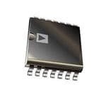
| 产品图片 |
|
| rohs | 符合RoHS无铅 / 符合限制有害物质指令(RoHS)规范要求 |
| 产品系列 | 数字电位计 IC,Analog Devices AD5252BRUZ1- |
| 数据手册 | |
| 产品型号 | AD5252BRUZ1 |
| POT数量 | Dual |
| 产品目录页面 | |
| 产品种类 | 数字电位计 IC |
| 供应商器件封装 | 14-TSSOP |
| 包装 | 管件 |
| 商标 | Analog Devices |
| 存储器类型 | 非易失 |
| 安装类型 | 表面贴装 |
| 安装风格 | SMD/SMT |
| 容差 | 30 % |
| 封装 | Tube |
| 封装/外壳 | 14-TSSOP(0.173",4.40mm 宽) |
| 封装/箱体 | TSSOP-14 |
| 工作温度 | -40°C ~ 85°C |
| 工作电源电压 | 2.75 V |
| 工厂包装数量 | 96 |
| 弧刷存储器 | Non Volatile |
| 抽头 | 256 |
| 接口 | I²C(设备位址) |
| 数字接口 | I2C |
| 最大工作温度 | + 85 C |
| 最小工作温度 | - 40 C |
| 标准包装 | 96 |
| 每POT分接头 | 256 |
| 温度系数 | 300 PPM / C |
| 电压-电源 | 2.7 V ~ 5.5 V, ±2.25 V ~ 2.75 V |
| 电源电压-最大 | 5.5 V |
| 电源电压-最小 | 2.7 V |
| 电源电流 | 3 uA |
| 电路数 | 2 |
| 电阻 | 1 kOhms |
| 电阻(Ω) | 1k |
| 系列 | AD5252 |


- 商务部:美国ITC正式对集成电路等产品启动337调查
- 曝三星4nm工艺存在良率问题 高通将骁龙8 Gen1或转产台积电
- 太阳诱电将投资9.5亿元在常州建新厂生产MLCC 预计2023年完工
- 英特尔发布欧洲新工厂建设计划 深化IDM 2.0 战略
- 台积电先进制程称霸业界 有大客户加持明年业绩稳了
- 达到5530亿美元!SIA预计今年全球半导体销售额将创下新高
- 英特尔拟将自动驾驶子公司Mobileye上市 估值或超500亿美元
- 三星加码芯片和SET,合并消费电子和移动部门,撤换高东真等 CEO
- 三星电子宣布重大人事变动 还合并消费电子和移动部门
- 海关总署:前11个月进口集成电路产品价值2.52万亿元 增长14.8%


PDF Datasheet 数据手册内容提取
Dual 64-/256-Position I2C Nonvolatile Memory Digital Potentiometers Data Sheet AD5251/AD5252 FEATURES FUNCTIONAL BLOCK DIAGRAM AD5251: Dual 64-position resolution AD5252: Dual 256-position resolution VDD RDAC EEMEM RDAC1 RDAC1 A1 VSS EEMEM RAB REGIS- W1 AD5251: 50 kΩ DGND PROEWFERRE-SOHN TOL TER B1 AD5252: 1 kΩ, 10 kΩ, 50 kΩ, 100 kΩ WP Nonvolatile memory1 stores wiper setting w/write protection SCL DATA RDAC3 RDAC3 A3 Power-on refreshed with EEMEM settings in 300 µs typ SDA I2C REGIS- W3 EEMEM rewrite time = 540 µs typ INTSEERRFIAALCE CONTROL TER B3 AD0 COMMAND Resistance tolerance stored in nonvolatile memory AD1 DECODE LOGIC 12 extra bytes in EEMEM for user-defined information ADDRESS DECODE LOGIC AD5251/ IDP2rCier-edccoetmf rinepeaaddt i/lbwinlreei taseer raiincaccler iensmst eoerfnf Rat/cDdeAe Ccr2e amnden EtE cMoEmMm raengdisst ers OPNO RWEESRE-T CONTROL LOGIC AD5252 03823-0-001 Figure 1. Predefined ±6 dB step change commands Synchronous or asynchronous dual-channel update and extra EEMEM for storing user-defined information, such as Wiper setting readback memory data for other components, look-up table, or system 4 MHz bandwidth—1 kΩ version identification information. Single supply 2.7 V to 5.5 V The AD5251/AD5252 allow the host I2C controllers to write Dual supply ±2.25 V to ±2.75 V any of the 64-/256-step wiper settings in the RDAC registers 2 slave address decoding bits allow operation of 4 devices and store them in the EEMEM. Once the settings are stored, 100-year typical data retention, T = 55°C A they are restored automatically to the RDAC registers at system Operating temperature: –40°C to +105°C power-on; the settings can also be restored dynamically. APPLICATIONS The AD5251/AD5252 provide additional increment, Mechanical potentiometer replacement decrement, +6 dB step change, and –6 dB step change in General-purpose DAC replacement synchronous or asynchronous channel update mode. The LCD panel V adjustment increment and decrement functions allow stepwise linear COM White LED brightness adjustment adjustments, with a ± 6 dB step change equivalent to doubling RF base station power amp bias control or halving the RDAC wiper setting. These functions are useful Programmable gain and offset control for steep-slope, nonlinear adjustments, such as white LED Programmable voltage-to-current conversion brightness and audio volume control. Programmable power supply The AD5251/AD5252 have a patented resistance-tolerance Sensor calibrations storing function that allows the user to access the EEMEM and GENERAL DESCRIPTION obtain the absolute end-to-end resistance values of the RDACs for precision applications. The AD5251/AD5252 are dual-channel, I2C®, nonvolatile mem- ory, digitally controlled potentiometers with 64/256 positions, The AD5251/AD5252 are available in TSSOP-14 packages. respectively. These devices perform the same electronic adjust- AD5251 has only 50 kΩ resistance options and AD5252 is ment functions as mechanical potentiometers, trimmers, and available in 1 kΩ, 10 kΩ, 50 kΩ, and 100 kΩ options. All parts variable resistors. The parts’ versatile programmability allows are guaranteed to operate over the –40°C to +105°C extended multiple modes of operation, including read/write access in the industrial temperature range. RDAC and EEMEM registers, increment/decrement of resistance, resistance changes in ±6 dB scales, wiper setting readback, 1 The terms nonvolatile memory and EEMEM are used interchangeably. 2 The terms digital potentiometer and RDAC are used interchangeably. Rev. E Document Feedback Information furnished by Analog Devices is believed to be accurate and reliable. However, no responsibility is assumed by Analog Devices for its use, nor for any infringements of patents or other One Technology Way, P.O. Box 9106, Norwood, MA 02062-9106, U.S.A. rights of third parties that may result from its use. Specifications subject to change without notice. No license is granted by implication or otherwise under any patent or patent rights of Analog Devices. Tel: 781.329.4700 ©2004–2017 Analog Devices, Inc. All rights reserved. Trademarks and registered trademarks are the property of their respective owners. Technical Support www.analog.com
AD5251/AD5252 Data Sheet TABLE OF CONTENTS Features .............................................................................................. 1 Theory of Operation ...................................................................... 21 Applications ....................................................................................... 1 Linear Increment/Decrement Commands ............................. 21 General Description ......................................................................... 1 ±6 dB Adjustments (Doubling/Halving Wiper Setting) ....... 21 Functional Block Diagram .............................................................. 1 Digital Input/Output Configuration........................................ 21 Revision History ............................................................................... 2 Multiple Devices on One Bus ................................................... 22 Electrical Characteristics ................................................................. 3 Terminal Voltage Operation Range ......................................... 22 1 kΩ Version .................................................................................. 3 Power-Up and Power-Down Sequences .................................. 22 10 kΩ, 50 kΩ, 100 kΩ Versions .................................................. 5 Layout and Power Supply Biasing ............................................ 23 Interface Timing Characteristics ................................................ 7 Digital Potentiometer Operation ............................................. 23 Absolute Maximum Ratings ............................................................ 8 Programmable Rheostat Operation ......................................... 23 ESD Caution .................................................................................. 8 Programmable Potentiometer Operation ............................... 24 Pin Configuration and Function Descriptions ............................. 9 Applications Information .............................................................. 25 Typical Performance Characteristics ........................................... 10 LCD Panel V Adjustment .................................................... 25 COM I2C Interface ..................................................................................... 14 Current-Sensing Amplifier ....................................................... 25 I2C Interface General Description ............................................ 14 Adjustable High Power LED Driver ........................................ 25 I2C Interface Detail Description ............................................... 15 Outline Dimensions ....................................................................... 26 I2C-Compatible 2-Wire Serial Bus ........................................... 20 Ordering Guide .......................................................................... 27 REVISION HISTORY 11/2017—Rev. D to Rev. E 9/2005—Rev. 0 to Rev. A Changes to Features Section and General Description Section ........ 1 Updated Format .................................................................. Universal Changes to Theory of Operation Section .................................... 21 Change to Figure 6 ......................................................................... 10 Changes to Ordering Guide .......................................................... 27 Changes to Figure 28 ...................................................................... 15 Changes to Figure 29 ...................................................................... 17 9/2012—Rev. C to Rev. D Changes to RDAC/EEMEM Quick Commands Section .......... 18 Changed Temperature Range from –40°C to +85°C to –40°C to Changes to EEMEM Write Protection Section .......................... 18 +105°C (Throughout) ...................................................................... 1 Changes to Figure 37 ...................................................................... 22 Changed WPEE Leakage Current from 5 µA to 8 µA, Table 1 ........ 4 Deleted Table 13 and Table 14 ...................................................... 23 AA Changed WPEE Leakage Current from 5 µA to 8 µA, Table 2 ........ 5 Change to Figure 42 ....................................................................... 24 AA AA Changes to Figure 11 and Figure 12 ............................................. 11 Change to Figure 46 ....................................................................... 25 Changes to Ordering Guide .......................................................... 27 12/2011—Rev. B to Rev. C Changes to Theory of Operation Section .................................... 21 6/2004—Revision 0: Initial Version Changes to Ordering Guide .......................................................... 27 10/2009—Rev. A to Rev. B Changes to Figure 15 ...................................................................... 12 Changes to Figure 27 ...................................................................... 15 Rev. E | Page 2 of 28
Data Sheet AD5251/AD5252 ELECTRICAL CHARACTERISTICS 1 kΩ VERSION V = 3 V ± 10% or 5 V ± 10%, V = 0 V or V /V = ±2.5 V ± 10%, V = V , V = 0 V, –40°C < T < +105°C, unless otherwise noted. DD SS DD SS A DD B A Table 1. Parameter Symbol Conditions Min Typ1 Max Unit 2F2F DC CHARACTERISTICS— RHEOSTAT MODE Resolution N AD5251 6 Bits AD5252 8 Bits Resistor Differential Nonlinearity2 R-DNL R , R = NC, V = 5.5 V, AD5251 –0.5 ±0.2 +0.5 LSB 3F3F WB WA DD R , R = NC, V = 5.5 V, AD5252 –1.00 ±0.25 +1.00 LSB WB WA DD R , R = NC, V = 2.7 V, AD5251 –0.75 ±0.30 +0.75 LSB WB WA DD R , R = NC, V = 2.7 V, AD5252 –1.5 ±0.3 +1.5 LSB WB WA DD Resistor Nonlinearity2 R-INL R , R = NC, V = 5.5 V, AD5251 –0.5 ±0.2 +0.5 LSB WB WA DD R , R = NC, V = 5.5 V, AD5252 –2.0 ±0.5 +2.0 LSB WB WA DD R , R = NC, V = 2.7 V, AD5251 –1.0 +2.5 +4.0 LSB WB WA DD R , R = NC, V = 2.7 V, AD5252 –2 +9 +14 LSB WB WA DD Nominal Resistor Tolerance ΔR /R T = 25°C –30 +30 % AB AB A Resistance Temperature (ΔR /R ) × 106/ΔT 650 ppm/°C AB AB Coefficient Wiper Resistance R I = 1 V/R, V = 5 V 75 130 Ω W W DD I = 1 V/R, V = 3 V 200 300 Ω W DD Channel-Resistance Matching ΔR /ΔR 0.15 % AB1 AB3 DC CHARACTERISTICS— POTENTIOMETER DIVIDER MODE Differential Nonlinearity3 DNL AD5251 –0.5 ±0.1 +0.5 LSB 4F AD5252 –1.00 ±0.25 +1.00 LSB Integral Nonlinearity3 INL AD5251 –0.5 ±0.2 +0.5 LSB AD5252 –2.0 ±0.5 +2.0 LSB Voltage Divider Tempco (ΔV /V ) × 106/ΔT Code = half scale 25 ppm/°C W W Full-Scale Error V Code = full scale, V = 5.5 V, –5 –3 0 LSB WFSE DD AD5251 Code = full scale, V = 5.5 V, –16 –11 0 LSB DD AD5252 Code = full scale, V = 2.7 V, −6 –4 0 LSB DD AD5251 Code = full scale, V = 2.7 V, –23 –16 0 LSB DD AD5252 Zero-Scale Error V Code = zero scale, V = 5.5 V, 0 3 5 LSB WZSE DD AD5251 Code = zero scale, V = 5.5 V, 0 11 16 LSB DD AD5252 Code = zero scale, V = 2.7 V, 0 4 6 LSB DD AD5251 Code = zero scale, V = 2.7 V, 0 15 20 LSB DD AD5252 RESISTOR TERMINALS Voltage Range4 V , V , V V V V 5F A B W SS DD Capacitance5 A, B C , C f = 1 kHz, measured to GND, 85 pF 6F A B code = half scale Capacitance5 W C f = 1 kHz, measured to GND, 95 pF W code = half scale Common-Mode Leakage Current I V = V = V /2 0.01 1 µA CM A B DD Rev. E | Page 3 of 28
AD5251/AD5252 Data Sheet Parameter Symbol Conditions Min Typ1 Max Unit 2F2F DIGITAL INPUTS AND OUTPUTS Input Logic High V V = 5 V, V = 0 V 2.4 V IH DD SS V /V = 2.7 V/0 V or V /V = ± 2.5 2.1 V DD SS DD SS V Input Logic Low V V = 5 V, V = 0 V 0.8 V IL DD SS Output Logic High (SDA) V R = 2.2 kΩ to V = 5 V, V = 0 4.9 V OH PULL-UP DD SS V Output Logic Low (SDA) V R = 2.2 kΩ to V = 5 V, V = 0 0.4 V OL PULL-UP DD SS V AAWPEE AALeakage Current IWP AAWPEE AA= VDD 8 µA A0 Leakage Current I A0 = GND 3 µA A0 Input Leakage Current I V = 0 V or V ±1 µA I IN DD (Other than WPEE and A0) AA AA Input Capacitance5 C 5 pF I POWER SUPPLIES Single-Supply Power Range V V = 0 V 2.7 5.5 V DD SS Dual-Supply Power Range V /V ±2.25 ±2.75 V DD SS Positive Supply Current I V = V or V = GND 5 15 µA DD IH DD IL Negative Supply Current I V = V or V = GND, V = 2.5 V, –5 –15 µA SS IH DD IL DD V = –2.5 V SS EEMEM Data Storing Mode I V = V or V = GND 35 mA DD_STORE IH DD IL Current EEMEM Data Restoring Mode I V = V or V = GND 2.5 mA DD_RESTORE IH DD IL Current6 7F Power Dissipation7 P V = V = 5 V or V = GND 0.075 mW 8F DISS IH DD IL Power Supply Sensitivity PSS ΔV = 5 V ± 10% −0.025 +0.010 +0.025 %/% DD ΔV = 3 V ± 10% –0.04 +0.02 +0.04 %/% DD DYNAMIC CHARACTERISTICS5, 8 9F Bandwidth –3 dB BW R = 1 kΩ 4 MHz AB Total Harmonic Distortion THD V = 1 V rms, V = 0 V, f = 1 kHz 0.05 % A B V Settling Time t V = V , V = 0 V 0.2 µs W S A DD B Resistor Noise Voltage eN_WB RWB = 500 Ω, f = 1 kHz 3 nV/√AAHzEE (thermal noise only) Digital Crosstalk C V = V , V = 0 V, measure V with –80 dB T A DD B W adjacent RDAC making full-scale change Analog Coupling C Signal input at A1 and measure –72 dB AT the output at W3, f = 1 kHz 1 Typical values represent average readings at 25°C and VDD = 5 V. 2 Resistor position nonlinearity error (R-INL) is the deviation from an ideal value measured between the maximum and minimum resistance wiper positions. R-DNL is the relative step change from an ideal value measured between successive tap positions. Parts are guaranteed monotonic, except R-DNL of AD5252 1 kΩ version at VDD = 2.7 V, IW = VDD/R for both VDD = 3 V and VDD = 5 V. 3 INL and DNL are measured at VW with the RDAC configured as a potentiometer divider, similar to a voltage output digital-to-analog converter. VA = VDD and VB = 0 V. DNL specification limits of ±1 LSB maximum are guaranteed monotonic operating conditions. 4 Resistor Terminal A, Terminal B, and Terminal W have no limitations on polarity with respect to each other. 5 Guaranteed by design and not subject to production test. 6 Command 0 NOP should be activated after Command 1 to minimize IDD_READ current consumption. 7 PDISS is calculated from IDD × VDD = 5 V. 8 All dynamic characteristics use VDD = 5 V. Rev. E | Page 4 of 28
Data Sheet AD5251/AD5252 10 kΩ, 50 kΩ, 100 kΩ VERSIONS V = +3 V ± 10% or +5 V ± 10%, V = 0 V or V /V = ± 2.5 V ± 10%, V = V , V = 0 V, –40°C < T < +105°C, unless otherwise noted. DD SS DD SS A DD B A Table 2. Parameter Symbol Conditions Min Typ1 Max Unit 10F DC CHARACTERISTICS— RHEOSTAT MODE Resolution N AD5251 6 Bits AD5252 8 Bits Resistor Differential Nonlinearity2 R-DNL R , R = NC, AD5251 −0.75 ±0.10 +0.75 LSB 11F WB WA R , R = NC, AD5252 −1.00 ±0.25 +1.00 LSB WB WA Resistor Nonlinearity2 R-INL R , R = NC, AD5251 −0.75 ±0.25 +0.75 LSB WB WA R , R = NC, AD5252 −2.5 ±1.0 +2.5 LSB WB WA Nominal Resistor Tolerance ΔR /R T = 25°C −20 +20 % AB AB A Resistance Temperature (ΔR /R ) × 106/ΔT 650 ppm/°C AB AB Coefficient Wiper Resistance R I = 1 V/R, V = 5 V 75 130 Ω W W DD I = 1 V/R, V = 3 V 200 300 Ω W DD Channel-Resistance Matching ΔR /ΔR R = 10 kΩ, 50 kΩ 0.15 % AB1 AB2 AB R = 100 kΩ 0.05 % AB DC CHARACTERISTICS— POTENTIOMETER DIVIDER MODE Differential Nonlinearity3 DNL AD5251 −0.5 ±0.1 +0.5 LSB 12F AD5252 −1.0 ±0.3 +1.0 LSB Integral Nonlinearity3 INL AD5251 −0.50 ±0.15 +0.50 LSB AD5252 −1.5 ±0.5 +1.5 LSB Voltage Divider (ΔV /V ) × 106/ΔT Code = half scale 15 ppm/°C W W Temperature Coefficient Full-Scale Error V Code = full scale, AD5251 −1.0 −0.3 0 LSB WFSE Code = full scale, AD5252 −3 −1 0 LSB Zero-Scale Error V Code = zero scale, AD5251 0 0.3 1.0 LSB WZSE Code = zero scale, AD5252 0 1.2 3.0 LSB RESISTOR TERMINALS Voltage Range4 V , V , V V V V 13F A B W SS DD Capacitance5 A, B C , C f = 1 kHz, measured to GND, 85 pF 14F A B code = half scale Capacitance5 W C f = 1 kHz, measured to GND, 95 pF W code = half scale Common-Mode Leakage Current I V = V = V /2 0.01 1.00 µA CM A B DD DIGITAL INPUTS AND OUTPUTS Input Logic High V V = 5 V, V = 0 V 2.4 V IH DD SS V /V = +2.7 V/0 V or V /V = ±2.5 V 2.1 V DD SS DD SS Input Logic Low V V = 5 V, V = 0 V 0.8 V IL DD SS V /V = +2.7 V/0 V or V /V = ±2.5 V 0.6 V DD SS DD SS Output Logic High (SDA) V R = 2.2 kΩ to V = 5 V, V = 0 V 4.9 V OH PULL-UP DD SS Output Logic Low (SDA) V R = 2.2 kΩ to V = 5 V, V = 0 V 0.4 V OL PULL-UP DD SS AAWPEE AALeakage Current IWP AAWPEEAA = VDD 8 µA A0 Leakage Current I A0 = GND 3 µA A0 Input Leakage Current I V = 0 V or V ±1 µA I IN DD (Other than WPEE and A0) AA AA Input Capacitance5 C 5 pF I Rev. E | Page 5 of 28
AD5251/AD5252 Data Sheet Parameter Symbol Conditions Min Typ1 Max Unit 10F POWER SUPPLIES Single-Supply Power Range V V = 0 V 2.7 5.5 V DD SS Dual-Supply Power Range V /V ±2.25 ±2.75 V DD SS Positive Supply Current I V = V or V = GND 5 15 µA DD IH DD IL Negative Supply Current I V = V or V = GND, V = 2.5 V, −5 −15 µA SS IH DD IL DD V = −2.5 V SS EEMEM Data Storing Mode I V = V or V = GND, T = 0°C to 105°C 35 mA DD_STORE IH DD IL A Current EEMEM Data Restoring Mode I V = V or V = GND, T = 0°C to 105°C 2.5 mA DD_RESTORE IH DD IL A Current6 15F Power Dissipation7 P V = V = 5 V or V = GND 0.075 mW 16F DISS IH DD IL Power Supply Sensitivity PSS ΔV = 5 V ± 10% −0.005 +0.002 +0.005 %/% DD ΔV = 3 V ± 10% −0.010 +0.002 +0.010 %/% DD DYNAMIC CHARACTERISTICS5, 8 17F –3 dB Bandwidth BW R = 10 kΩ/50 kΩ/100 kΩ 400/80/40 kHz AB Total Harmonic Distortion THD V = 1 V rms, V = 0 V, f = 1 kHz 0.05 % W A B V Settling Time t V = V , V = 0 V, 1.5/7/14 µs W S A DD B R = 10 kΩ/50 kΩ/100 kΩ AB Resistor Noise Voltage eN_WB RAB = 10 kΩ/50 kΩ/100 kΩ, 9/20/29 nV/√AAHzEE code = midscale, f = 1 kHz (thermal noise only) Digital Crosstalk C V = V , V = 0 V, measure V with −80 dB T A DD B W adjacent RDAC making full-scale change Analog Coupling C Signal input at A1 and measure −72 dB AT output at W3, f = 1 kHz 1 Typical values represent average readings at 25°C and VDD = 5 V. 2 Resistor position nonlinearity error (R-INL) is the deviation from an ideal value measured between the maximum and minimum resistance wiper positions. R-DNL is the relative step change from an ideal value measured between successive tap positions. Parts are guaranteed monotonic, except R-DNL of AD5252 1 kΩ version at VDD = 2.7 V, IW = VDD/R for both VDD = 3 V and VDD = 5 V. 3 INL and DNL are measured at VW with the RDAC configured as a potentiometer divider, similar to a voltage output DAC. VA = VDD and VB = 0 V. DNL specification limits of ±1 LSB maximum are guaranteed monotonic operating conditions. 4 Resistor Terminal A, Terminal B, and Terminal W have no limitations on polarity with respect to each other. 5 Guaranteed by design and not subject to production test. 6 Command 0 NOP should be activated after Command 1 to minimize IDD_READ current consumption. 7 PDISS is calculated from IDD × VDD = 5 V. 8 All dynamic characteristics use VDD = 5 V. Rev. E | Page 6 of 28
Data Sheet AD5251/AD5252 INTERFACE TIMING CHARACTERISTICS All input control voltages are specified with t = t = 2.5 ns (10% to 90% of 3 V) and timed from a voltage level of 1.5 V. Switching R F characteristics are measured using both V = 3 V and 5 V. DD Table 3. Interface Timing and EEMEM Reliability Characteristics (All Parts)1 18F Parameter Symbol Conditions Min Typ Max Unit INTERFACE TIMING SCL Clock Frequency fSCL 400 kHz t Bus-Free Time Between Stop and Start t 1.3 µs BUF 1 tHD;STA Hold Time (Repeated Start) t2 After this period, the first clock pulse is 0.6 µs generated. tLOW Low Period of SCL Clock t3 1.3 µs tHIGH High Period of SCL Clock t4 0.6 µs tSU;STA Set-up Time for Start Condition t5 0.6 µs tHD;DAT Data Hold Time t6 0 0.9 µs tSU;DAT Data Set-up Time t7 100 ns tF Fall Time of Both SDA and SCL Signals t8 300 ns tR Rise Time of Both SDA and SCL Signals t9 300 ns tSU;STO Set-up Time for Stop Condition t10 0.6 µs EEMEM Data Storing Time t 26 ms EEMEM_STORE EEMEM Data Restoring Time at Power-On2 t V rise time dependent. Measure 300 µs 19F EEMEM_RESTORE1 DD without decoupling capacitors at V DD and V . SS EEMEM Data Restoring Time upon Restore t V = 5 V. 300 µs EEMEM_RESTORE2 DD Command or Reset Operation2 EEMEM Data Rewritable Time (Delay Time t 540 µs EEMEM_REWRITE After Power-On or Reset Before EEMEM Can Be Written) FLASH/EE MEMORY RELIABILITY Endurance3 100 k cycles 20F Data Retention4 100 Years 21F 1 Guaranteed by design; not subject to production test. See Figure 23 for location of measured values. 2 During power-up, all outputs are preset to midscale before restoring the EEMEM contents. RDAC0 has the shortest EEMEM data restoring time, whereas RDAC3 has the longest. 3 Endurance is qualified to 100,000 cycles per JEDEC Standard 22, Method A117, and measured at −40°C, +25°C, and +105°C; typical endurance at +25°C is 700,000 cycles. 4 Retention lifetime equivalent at junction temperature TJ = 55°C per JEDEC Std. 22, Method A117. Retention lifetime based on an activation energy of 0.6 eV derates with junction temperature in Flash/EE memory. Rev. E | Page 7 of 28
AD5251/AD5252 Data Sheet ABSOLUTE MAXIMUM RATINGS T = 25°C, unless otherwise noted. A Stresses at or above those listed under Absolute Maximum Ratings may cause permanent damage to the product. This is a Table 4. stress rating only; functional operation of the product at these Parameter Rating or any other conditions above those indicated in the operational V to GND −0.3 V, +7 V DD section of this specification is not implied. Operation beyond V to GND +0.3 V, −7 V SS the maximum operating conditions for extended periods may V to V 7 V DD SS affect product reliability. V , V , V to GND V , V A B W SS DD Maximum Current IWB, IWA Pulsed ±20 mA ESD CAUTION I Continuous (R ≤ 1 kΩ, A Open)1 ±5 mA WB WB 0F0F I Continuous (R ≤ 1 kΩ, B Open)1 ±5 mA WA WA I Continuous ±5 mA/±500 µA/ AB (R = 1 kΩ/10 kΩ/50 kΩ/100 kΩ)1 ±100 µA/±50 µA AB Digital Inputs and Output Voltage to GND 0 V, 7 V Operating Temperature Range −40°C to +105°C Maximum Junction Temperature (T ) 150°C JMAX Storage Temperature Range −65°C to +150°C Lead Temperature (Soldering, 10 sec) 300°C Vapor Phase (60 sec) 215°C Infrared (15 sec) 220°C TSSOP-14 Thermal Resistance2 θ 136°C/W 1F1F JA 1 Maximum terminal current is bound by the maximum applied voltage across any two of the A, B, and W terminals at a given resistance, the maximum current handling of the switches, and the maximum power dissipation of the package. VDD = 5 V. 2 Package power dissipation = (TJMAX − TA)/θJA. Rev. E | Page 8 of 28
Data Sheet AD5251/AD5252 PIN CONFIGURATION AND FUNCTION DESCRIPTIONS VDD 1 14 W3 AD0 2 13 B3 AD5251/ WP 3 12 A3 AD5252 W1 4 11 AD1 TOP VIEW B1 5 (Not to Scale) 10 DGND SDAA1 67 98 VSSCSL 03823-0-002 Figure 2. Pin Configuration Table 5. Pin Function Descriptions Pin No. Mnemonic Description 1 V Positive Power Supply Pin. Connect +2.7 V to +5 V for single supply or ±2.7 V for dual supply, where DD V – V ≤ 5.5 V. V must be able to source 35 mA for 26 ms when storing data to EEMEM. DD SS DD 2 AD0 I2C Device Address 0. AD0 and AD1 allow four AD5251/AD5252 devices to be addressed. 3 AAWPEE Write Protect, Active Low. VWP ≤ VDD + 0.3 V. 4 W1 Wiper Terminal of RDAC1. V ≤ V ≤ V .1 SS W1 DD22F 5 B1 B Terminal of RDAC1. V ≤ V ≤ V .1 SS B1 DD 6 A1 A Terminal of RDAC1. V ≤ V ≤ V .1 SS A1 DD 7 SDA Serial Data Input/Output Pin. Shifts in one bit at a time upon positive clock edges. MSB loaded first. Open-drain MOSFET requires pull-up resistor. 8 V Negative Supply. Connect to 0 V for single supply or –2.7 V for dual supply, where V – V ≤ +5.5 V. If SS DD SS V is used in dual supply, V must be able to sink 35 mA for 26 ms when storing data to EEMEM. SS SS 9 SCL Serial Input Register Clock Pin. Shifts in one bit at a time upon positive clock edges. V ≤ (V + 0.3 V). SCL DD Pull-up resistor is recommended for SCL to ensure minimum power. 10 DGND Digital Ground. Connect to system analog ground at a single point. 11 AD1 I2C Device Address 1. AD0 and AD1 allow four AD5251/AD5252 devices to be addressed. 12 A3 A Terminal of RDAC3. V ≤ V ≤ V .1 SS A3 DD 13 B3 B Terminal of RDAC3. V ≤ V ≤ V .1 SS B3 DD 14 W3 Wiper Terminal of RDAC3. V ≤ V ≤ V .1 SS W3 DD 1 For quad-channel device software compatibility, the dual potentiometers in the parts are designated as RDAC1 and RDAC3. Rev. E | Page 9 of 28
AD5251/AD5252 Data Sheet TYPICAL PERFORMANCE CHARACTERISTICS 1.0 1.0 0.8 0.8 TA=–40°C, +25°C, +85°C, +125°C 0.6 0.6 TA=–40°C, +25°C, +85°C, +125°C 0.4 0.4 SB) 0.2 B) 0.2 L S NL ( 0 L (L 0 R-I–0.2 DN–0.2 –0.4 –0.4 –0.6 –0.6 –0.8 –0.8 –1.00 32 64 9C6ODE 1(D28ecima1l)60 192 224 256 03823-0-015 –1.00 32 64 9C6ODE 1(D28ecima1l)60 192 224 256 03823-0-018 Figure 3. R-INL vs. Code Figure 6. DNL vs. Code 1.0 10 0.8 8 TA =–40°C, +25°C, +85°C, +125°C 0.6 6 IDD @ VDD= 5.5V 0.4 4 LSB) 0.2 A) 2 IDD @ VDD= 2.7V NL ( 0 µ (D 0 R-D–0.2 ID –2 –0.4 –4 ISS @ VDD= 2.7V, VSS=–2.7V –0.6 –6 –0.8 –8 –1.00 32 64 9C6ODE 1(D28ecima1l)60 192 224 256 03823-0-016 –10–40 –20 0 2T0EMPER40ATURE6 0(°C) 80 100 120 03823-0-019 Figure 4. R-DNL vs. Code Figure 7. Supply Current vs. Temperature 1.0 10 0.8 TA=–40°C, +25°C, +85°C, +125°C 0.6 1 VDD= 5.5V 0.4 0.2 0.1 B) A) INL (LS–0.20 I (mDD0.01 –0.4 VDD= 2.7V –0.6 0.001 –0.8 –1.00 32 64 9C6ODE 1(D28ecima1l)60 192 224 256 03823-0-017 0.00010 1 DIG2ITAL INPU3T VOLTAG4E (V) 5 6 03823-0-020 Figure 5. INL vs. Code Figure 8. Supply Current vs. Digital Input Voltage, TA = 25°C Rev. E | Page 10 of 28
Data Sheet AD5251/AD5252 240 50 220 DATA = 0x00 C) 45 VDD= 5V 210800 VTDAD== 2 25.°7CV O (ppm/° 40 VVTAAB === V0–V4D0D°C TO +85°C 160 PC 35 M Ω) 140 TE 30 R (WB110200 VTDAD== 2 55.°5CV R MODE 2205 80 TE 60 OME 15 100kΩ 10kΩ 40 NTI 10 E T 20 O 5 50kΩ P 00 1 2 VBIA3S(V) 4 5 6 03823-0-021 00 32 64 9C6ODE 1(D28ecima1l)60 192 224 256 03823-0-024 Figure 9. Wiper Resistance vs. VBIAS Figure 12. AD5252 Potentiometer Mode Tempco ∆VWB/∆T vs. Code 6 0 0xFF –6 0x80 4 0x40 –12 0x20 –18 0x10 2 ∆R (%)WB 0 GAIN (dB) –––233460 0x08 0x04 0x02 –2 –42 0x01 0x00 –48 –4 –54 –6–40 –20 0 T2E0MPERA40TURE (6°0C) 80 100 120 03823-0-022 –6010 100 1k FREQ1U0kENCY (1H0z0)k 1M 10M 03823-0-025 Figure 10. Change of RWB vs. Temperature Figure 13. AD5252 Gain vs. Frequency vs. Code, RAB = 1 kΩ, TA = 25°C 1000 0 0xFF 950 VDD=5V –6 (ppm/°C) 895000 TVVAAB===V0–V4D0D°CTO+85°C ––1128 00xx8400 CO 0x20 ETEMP 785000 10kΩ N (dB) ––2340 00xx1008 MOD 700 100kΩ GAI –36 0x04 STAT 650 50kΩ –42 0x01 O HE 600 –48 0x00 R 550 –54 0x02 5000 32 64 9C6ODE1(D28ecima1l6)0 192 224 256 03823-0-023 –6010 100 1kFREQU1E0NkCY (Hz1)00k 1M 10M 03823-0-026 Figure 11. AD5252 Rheostat Mode Tempco ∆RWB/∆T vs. Code Figure 14. AD5252 Gain vs. Frequency vs. Code, RAB = 10 kΩ , TA = 25°C Rev. E | Page 11 of 28
AD5251/AD5252 Data Sheet 0 1.2 –6 0xFF TA= 25°C 0x80 1.0 –12 0x40 –18 0x20 0.8 GAIN (dB) –––233460 00xx1008 I (mA)DD 0.6 VDD= 5.5V 0x04 0.4 –42 0x02 –48 0x01 0.2 VDD= 2.7V –54 0x00 –6010 100 1kFREQU1E0NkCY (Hz1)00k 1M 10M 03823-0-027 01 10 100CLOC1Kk FREQ1U0EkNCY (1H0z0)k 1M 10M 03823-0-030 Figure 15. AD5252 Gain vs. Frequency vs. Code, RAB = 50 kΩ , TA = 25°C Figure 18. Supply Current vs. Digital Input Clock Frequency 0 0x80 0xFF CLK –6 0x40 VDD = 5V –12 0x20 –18 0x10 B) –24 d 0x08 N ( –30 GAI –36 0x04 VW 0x02 –42 DIGITAL FEEDTHROUGH 0x01 –48 –54 0x00 –6010 100 1kFREQU1E0NkCY (Hz1)00k 1M 10M03823-0-028 400ns/DIV 03823-0-031 Figure 16. AD5252 Gain vs. Frequency vs. Code, RAB = 100 kΩ , TA = 25°C Figure 19. Clock Feedthrough and Midscale Transition Glitch 100 VDD = 5.5V 80 100k 60 VDD (NO DE- 40 10k RESTORE RDAC1 COUPLING SETTING TO 0x3F CAPS) 20 MIDSCALE ) 1k PRESET VWB1 (AB 0 RESTORE RDAC3 (S0TxO3FRED R –20 SETTING TO 0x3F IN EEMEM) 50k MIDSCALE –40 PRESET VWB3 (0x3F –60 STORED VDD = VA1 = VA3 = 3.3V IN EEMEM) –80 GND = VB1 = VB3 –1000 32 64 9C6ODE 1(D28ecima1l)60 192 224 256 03823-0-029 03823-0-032 Figure 17. AD5252 ΔRAB vs. Code, TA = 25°C Figure 20. tEEMEM_RESTORE of RDAC0 and RDAC3 Rev. E | Page 12 of 28
Data Sheet AD5251/AD5252 6 6 5 RAB= 1kΩ 5 RAB= 1kΩ A) A) m m (B_MAX 4 TVAA== 2V5B°C=OPEN (B_MAX 4 VTAA== 2V5B°C=OPEN W W L I 3 L I 3 A A C C TI TI ORE 2 RAB= 10kΩ ORE 2 RAB= 10kΩ E E H H T T 1 RAB= 50kΩ 1 RAB= 50kΩ RAB= 100kΩ RAB= 100kΩ 00 8 16 24CODE3 2(Decim4a0l) 48 56 64 03823-0-033 00 32 64 96COD1E2 (8Decim1a6l0) 192 224 256 03823-0-034 Figure 21. AD5251 IWB_MAX vs. Code Figure 22. AD5252 IWB_MAX vs. Code Rev. E | Page 13 of 28
AD5251/AD5252 Data Sheet I2C INTERFACE t8 t6 t9 t2 SCL t2 t3 t4 t7 t5 t10 t8 t9 SDA P t1 S S P 03823-0-003 Figure 23. I2C Interface Timing Diagram I2C INTERFACE GENERAL DESCRIPTION FROM MASTER TO SLAVE FROM SLAVE TO MASTER S = START CONDITION P = STOP CONDITION A = ACKNOWLEDGE (SDA LOW) A = NOT ACKNOWLEDGE (SDA HIGH) R/W = READ ENABLE AT HIGH AND WRITE ENABLE AT LOW SLAVE ADDRESS INSTRUCTIONS DATA S R/W A A A/A P (7-BIT) (8-BIT) (8-BIT) 0 WRITE (N BDYATTEAS T+R AACNKSNFOEWRRLEEDDGE) 03823-0-004 Figure 24. I2C—Master Writing Data to Slave SLAVE ADDRESS DATA DATA S R/W A A A P (7-BIT) (8-BIT) (8-BIT) 1 READ (N BDYATTEAS T+R AACNKSNFOEWRRLEEDDGE) 03823-0-005 Figure 25. I2C—Master Reading Data from Slave SLAVE ADDRESS S R/W A DATA A/A S SLAVE ADDRESS R/W A DATA A/A P (7-BIT) READ OR WRITE (N BYTES + REPEATED START READ (N BYTES + 03823-0-006 ACKNOWLEDGE) OR WRITE ACKNOWLEDGE) DIRECTION OF TRANSFER MAY CHANGE AT THIS POINT Figure 26. I2C—Combined Write/Read Rev. E | Page 14 of 28
Data Sheet AD5251/AD5252 I2C INTERFACE DETAIL DESCRIPTION FROM MASTERTO SLAVE FROM SLAVETO MASTER S = START CONDITION P = STOP CONDITION A =ACKNOWLEDGE (SDA LOW) A = NOTACKNOWLEDGE (SDA HIGH) R/W = READ ENABLEAT HIGHAND WRITE ENABLEAT LOW CMD/REG = COMMAND ENABLE BIT, LOGIC HIGH/REGISTERACCESS BIT, LOGIC LOW EE/RDAC = EEMEM REGISTER, LOGIC HIGH/RDAC REGISTER, LOGIC LOW A4,A3,A2,A1,A0 = RDAC/EEMEM REGISTERADDRESSES S 0 1 0 1 1 A A 0 A CMD/ 0 EE/ A A A A A A DATA A/ P D D REG RDAC 4 3 2 1 0 A 1 0 SLAVEADDRESS 0 WRITE IANNSDTRAUDCDTRIOENSSS ACK(1N OBYWTLEE +DGE) 03823-0-007 0 REG Figure 27. Single Write Mode S 0 1 0 1 1 A A 0 A CMD/ 0 EE/ A A A A A A RDAC1 A X A RDAC3 A/ P D D REG RDAC 4 3 2 1 0 DATA DATA DATA A 1 0 RDAC SLAVE ADDRESS0 WRITE RDAACN IDN SATDRDURCETSISONS AC(KNN BOYWTLEESD +GE) 03823-0-008 0 REG Figure 28. Consecutive Write Mode Table 6. Addresses for Writing Data Byte Contents to RDAC Registers (R/WE = 0, CMD/REGE = 0, EE/RDACE = 0) A A A A A A A4 A3 A2 A1 A0 RDAC Data Byte Description 0 0 0 0 0 Reserved 0 0 0 0 1 RDAC1 6-/8-bit wiper setting (2 MSB of AD5251 are X) 0 0 0 1 0 Reserved 0 0 0 1 1 RDAC3 6-/8-bit wiper setting (2 MSB of AD5251 are X) 0 0 1 0 0 Reserved : : : : : : : : : : : : 0 1 1 1 1 Reserved Rev. E | Page 15 of 28
AD5251/AD5252 Data Sheet RDAC/EEMEM Write Table 7. Addresses for Writing (Storing) RDAC Settings Setting the wiper position requires an RDAC write operation. and User-Defined Data to EEMEM Registers The single write operation is shown in Figure 27, and the (R/WEE = 0, CMD/REGEE = 0, EE/RDACEE = 1) AA AA AA AA AA consecutive write operation is shown in Figure 28. In the A4 A3 A2 A1 A0 Data Byte Description consecutive write operation, if the AARDACEEAA is selected and the 0 0 0 0 0 Reserved address starts at 00001, the first data byte goes to RDAC1 and 0 0 0 0 1 Store RDAC1 setting to EEMEM11 23F the second data byte goes to RDAC3. The RDAC address is 0 0 0 1 0 Reserved shown in Table 6. 0 0 0 1 1 Store RDAC3 setting to EEMEM31 While the RDAC wiper setting is controlled by a specific RDAC 0 0 1 0 0 Store user data to EEMEM4 register, each RDAC register corresponds to a specific EEMEM 0 0 1 0 1 Store user data to EEMEM5 location, which provides nonvolatile wiper storage functionality. 0 0 1 1 0 Store user data to EEMEM6 The addresses are shown in Table 7. The single and consecutive 0 0 1 1 1 Store user data to EEMEM7 write operations also apply to EEMEM write operations. 0 1 0 0 0 Store user data to EEMEM8 0 1 0 0 1 Store user data to EEMEM9 There are 12 nonvolatile memory locations: EEMEM4 to 0 1 0 1 0 Store user data to EEMEM10 EEMEM15. Users can store a total of 12 bytes of information, 0 1 0 1 1 Store user data to EEMEM11 such as memory data for other components, look-up tables, or 0 1 1 0 0 Store user data to EEMEM12 system identification information. 0 1 1 0 1 Store user data to EEMEM13 In a write operation to the EEMEM registers, the device disables 0 1 1 1 0 Store user data to EEMEM14 the I2C interface during the internal write cycle. Acknowledge 0 1 1 1 1 Store user data to EEMEM15 polling is required to determine the completion of the write Users can store any of the 64 RDAC settings directly to the EEMEM for AD5251, cycle. See the EEMEM Write-Acknowledge Polling section. or any of the 256 RDAC settings directly to the EEMEM for the AD5252. This is not limited to current RDAC wiper setting. RDAC/EEMEM Read Table 8. Addresses for Reading (Restoring) RDAC Settings The AD5251/AD5252 provide two different RDAC or EEMEM and User Data from EEMEM read operations. For example, Figure 29 shows the method of (R/WEE = 1, CMD/REGEE = 0, EE/RDACEE = 1) reading the RDAC0 to RDAC3 contents without specifying the AA AA AA AA AA AA A4 A3 A2 A1 A0 Data Byte Description address, assuming Address RDAC0 was already selected in the previous operation. If an RDAC_N address other than RDAC0 0 0 0 0 0 Reserved was previously selected, readback starts with Address N, followed 0 0 0 0 1 Read RDAC1 setting from EEMEM1 by N + 1, and so on. 0 0 0 1 0 Reserved 0 0 0 1 1 Read RDAC3 setting from EEMEM3 Figure 30 illustrates a random RDAC or EEMEM read 0 0 1 0 0 Read user data from EEMEM4 operation. This operation allows users to specify which RDAC 0 0 1 0 1 Read user data from EEMEM5 or EEMEM register is read by issuing a dummy write command 0 0 1 1 0 Read user data from EEMEM6 to change the RDAC address pointer and then proceeding with 0 0 1 1 1 Read user data from EEMEM7 the RDAC read operation at the new address location. 0 1 0 0 0 Read user data from EEMEM8 0 1 0 0 1 Read user data from EEMEM9 0 1 0 1 0 Read user data from EEMEM10 0 1 0 1 1 Read user data from EEMEM11 0 1 1 0 0 Read user data from EEMEM12 0 1 1 0 1 Read user data from EEMEM13 0 1 1 1 0 Read user data from EEMEM14 0 1 1 1 1 Read user data from EEMEM15 Rev. E | Page 16 of 28
Data Sheet AD5251/AD5252 S 0 1 0 1 1 A A 1 A RDAC1 A X A RDAC3 A/ P D D EEMEM OR REGISTER DATA DATA EEMEM OR REGISTER DATA A 1 0 SLAVE ADDRESS 1 READ (N BYTES + ACKNOWLEDGE) 03823-0-009 Figure 29. RDAC Current Read (Restricted to Previously Selected Address Stored in the Register) S SLAVE ADDRESS 0 A INSTRUCTION AND A S SLAVE ADDRESS 1 A RDAC OR A/A P ADDRESS EEMEM DATA 0 WRITE REPEATED START 1 READ (N BYTES + ACKNOWLEDGE) 03823-0-010 Figure 30. RDAC or EEMEM Random Read FROM MASTER TO SLAVE FROM SLAVE TO MASTER S = START CONDITION P = STOP CONDITION A = ACKNOWLEDGE (SDA LOW) A = NOT ACKNOWLEDGE (SDA HIGH) AD1, AD0 = I2C DEVICE ADDRESS BITS; MUST MATCH WITH THE LOGIC STATES AT PINS AD1, AD0 R/W = READ ENABLE BIT, LOGIC HIGH/WRITE ENABLE BIT, LOGIC LOW CMD/REG = COMMAND ENABLE BIT, LOGIC HIGH/REGISTER ACCESS BIT, LOGIC LOW C3, C2, C1, C0 = COMMAND BITS A2, A1, A0 = RDAC/EEMEM REGISTER ADDRESSES S 0 1 0 1 1 A A 0 A CMD/ C C C C A A A A P D D REG 3 2 1 0 2 1 0 1 0 RDAC SLAVE ADDRESS0 WRITE 1 CMD 03823-0-011 Figure 31. RDAC Quick Command Write (Dummy Write) Rev. E | Page 17 of 28
AD5251/AD5252 Data Sheet RDAC/EEMEM Quick Commands For the second byte in Register N + 1, all eight data bits are designated for the decimal portion of tolerance. As shown in The AD5251/AD5252 feature 12 quick commands that facilitate Table 10 and Figure 32, for example, if the rated R is 10 kΩ easy manipulation of RDAC wiper settings and provide RDAC- AB and the data readback from Address 11000 shows 0001 1100 to-EEMEM storing and restoring functions. The command and Address 11001 shows 0000 1111, then RDAC0 tolerance format is shown in Figure 31, and the command descriptions can be calculated as are shown in Table 9. MSB: 0 = + When using a quick command, issuing a third byte is not needed, Next 7 MSB: 001 1100 = 28 but is allowed. The quick commands reset and store RDAC to 8 LSB: 0000 1111 = 15 × 2–8 = 0.06 EEMEM require acknowledge polling to determine whether the Tolerance = 28.06% and, therefore, command has finished executing. R = 12.806 kΩ R Tolerance Stored in Read-Only Memory AB_ACTUAL AB EEMEM Write-Acknowledge Polling The AD5251/AD5252 feature patented R tolerances storage in AB After each write operation to the EEMEM registers, an the nonvolatile memory. The tolerance of each channel is stored internal write cycle begins. The I2C interface of the device is in the memory during the factory production and can be read disabled. To determine if the internal write cycle is complete by users at any time. The knowledge of the stored tolerance, and the I2C interface is enabled, interface polling can be which is the average of R over all codes (see Figure 16), allows AB executed. I2C interface polling can be conducted by sending a users to predict R accurately. This feature is valuable for AB start condition, followed by the slave address and the write bit. precision, rheostat mode, and open-loop applications in which If the I2C interface responds with an ACK, the write cycle is knowledge of absolute resistance is critical. complete and the interface is ready to proceed with further The stored tolerances reside in the read-only memory and are operations. Other-wise, I2C interface polling can be repeated expressed as percentages. Each tolerance is stored in two memory until it succeeds. Command 2 and Command 7 also require locations (see Table 10 ). The tolerance data is expressed in sign acknowledge polling. magnitude binary format stored in two bytes; an example is shown EEMEM Write Protection in Figure 32. For the first byte in Register N, the MSB is designated for the sign (0 = + and 1 = –) and the 7 LSB is designated for the Setting the WPEE pin to logic low after EEMEM programming AA AA integer portion of the tolerance. protects the memory and RDAC registers from future write operations. In this mode, the EEMEM and RDAC read operations function as normal. Table 9. RDAC-to-EEMEM Interface and RDAC Operation Quick Command Bits (CMD/REGEE = 1, A2 = 0) AA AA C3 C2 C1 C0 Command Description 0 0 0 0 NOP 0 0 0 1 Restore EEMEM (A1, A0) to RDAC (A1, A0)1 24F 0 0 1 0 Store RDAC (A1, A0) to EEMEM (A1, A0) 0 0 1 1 Decrement RDAC (A1, A0) 6 dB 0 1 0 0 Decrement all RDACs 6 dB 0 1 0 1 Decrement RDAC (A1, A0) one step 0 1 1 0 Decrement all RDACs one step 0 1 1 1 Reset: restore EEMEMs to all RDACs 1 0 0 0 Increment RDACs (A1, A0) 6 dB 1 0 0 1 Increment all RDACs 6 dB 1 0 1 0 Increment RDACs (A1, A0) one step 1 0 1 1 Increment all RDACs one step 1 1 0 0 Reserved : : : : : : : : : : 1 1 1 1 Reserved 1 This command leaves the device in the EEMEM read power state, which consumes power. Issue the NOP command to return the device to its idle state. Rev. E | Page 18 of 28
Data Sheet AD5251/AD5252 Table 10. Address Table for Reading Tolerance (CMD/REGE = 0, EE/RDACE = 1, A4 = 1) A A A A A4 A3 A2 A1 A0 Data Byte Description 0 0 0 0 0 Reserved : : : : : : : : : : : : 1 1 0 0 1 Reserved 1 1 0 1 0 Sign and 7-bit integer values of RDAC1 tolerance (read only) 1 1 0 1 1 8-bit decimal value of RDAC1 tolerance (read only) 1 1 1 0 0 Reserved 1 1 1 0 1 Reserved 1 1 1 1 0 Sign and 7-bit integer values of RDAC3 tolerance (read only) 1 1 1 1 1 8-bit decimal value of RDAC3 tolerance (read only) A D7 D6 D5 D4 D3 D2 D1 D0 A D7 D6 D5 D4 D3 D2 D1 D0 A SIGN 26 25 24 23 22 21 20 2–1 2–2 2–3 2–4 2–5 2–6 2–7 2–8 SIGN 7 BITS FOR INTEGER NUMBER 8 BITS FOR DECIMAL NUMBER 03823-0-012 Figure 32. Format of Stored Tolerance in Sign Magnitude Format with Bit Position Descriptions (Unit Is Percent, Only Data Bytes Are Shown) Rev. E | Page 19 of 28
AD5251/AD5252 Data Sheet I2C-COMPATIBLE 2-WIRE SERIAL BUS 1 9 1 9 1 9 SCL SDA 0 1 0 1 1 AD1AD0 R/W X X X X X X X X D7 D6 D5 D4 D3 D2 D1 D0 ACK. BY ACK. BY ACK. BY STMAARSTT EBRY SLAVE FARDADMREE S1S BYTE AD525x INSTRFURCATMIOEN 2 BYTE AD525x DFARTAAM BEY T1E AD525xSMTAOSPT EBRY 03823-0-013 Figure 33. General I2C Write Pattern 1 9 1 9 SCL SDA 0 1 0 1 1 AD1AD0 R/W D7 D6 D5 D4 D3 D2 D1 D0 ACK. BY NO ACK. BY STMAARSTT BERY SLAVE FARDADMREE S1S BYTE AD525x RDAFCR RAEMGEI S2TER MASTESMRTAOSPT EBRY 03823-0-014 Figure 34. General I2C Read Pattern The first byte of the AD5251/AD5252 is a slave address byte the addresses of the EEMEM and RDAC registers (see (see Figure 33 and Figure 34). It has a 7-bit slave address and an Figure 27 and Figure 28). When MSB = 1 or when the device R/WEE bit. The 5 MSB of the slave address is 01011, and the next is in CMD mode, the four bits following the MSB are C3 to AA AA 2 LSB is determined by the states of the AD1 and AD0 pins. C1, which correspond to 12 predefined EEMEM controls AD1 and AD0 allow the user to place up to four and quick commands; there are also four factory-reserved AD5251/AD5252 devices on one bus. commands. The 3 LSB—A2, A1, and A0—are addresses, but only 001 and 011 are used for RDAC1 and RDAC3, AD5251/AD5252 can be controlled via an I2C-compatible serial respectively (see Figure 31). After acknowledging the bus and are connected to this bus as slave devices. The 2-wire instruction byte, the last byte in the write mode is the data I2C serial bus protocol (see Figure 33 and Figure 34) follows: byte. Data is transmitted over the serial bus in sequences of 1. The master initiates a data transfer by establishing a start nine clock pulses (eight data bits followed by an acknowledge condition, such that SDA goes from high to low while SCL bit). The transitions on the SDA line must occur during the is high (see Figure 33). The following byte is the slave address low period of SCL and remain stable during the high period byte, which consists of the 5 MSB of a slave address defined of SCL (see Figure 33). as 01011. The next two bits are AD1 and AD0, I2C device 3. In current read mode, the RDAC0 data byte immediately address bits. Depending on the states of their AD1 and follows the acknowledgment of the slave address byte. AD0 bits, four AD5251/AD5252 devices can be addressed After an acknowledgement, RDAC1 follows, then RDAC2, on the same bus. The last LSB, the R/WEE bit, determines AA AA and so on. (There is a slight difference in write mode, whether data is read from or written to the slave device. where the last eight data bits representing RDAC3 data are The slave whose address corresponds to the transmitted followed by a no acknowledge bit.) Similarly, the transitions address responds by pulling the SDA line low during the on the SDA line must occur during the low period of SCL ninth clock pulse (this is called an acknowledge bit). At and remain stable during the high period of SCL (see this stage, all other devices on the bus remain idle while Figure 34). Another reading method, random read the selected device waits for data to be written to or read method, is shown in Figure 30. from its serial register. 4. When all data bits have been read or written, a stop 2. In the write mode (except when restoring EEMEM to the condition is established by the master. A stop condition is RDAC register), there is an instruction byte that follows defined as a low-to-high transition on the SDA line that the slave address byte. The MSB of the instruction byte is occurs while SCL is high. In write mode, the master pulls labeled CMD/REGEE. MSB = 1 enables CMD, the command the SDA line high during the 10th clock pulse to establish a AA AA instruction byte; MSB = 0 enables general register writing. stop condition (see Figure 33). In read mode, the master The third MSB in the instruction byte, labeled EE/RDACEE, issues a no acknowledge for the ninth clock pulse, that is, AA AA is true when MSB = 0 or when the device is in general the SDA line remains high. The master brings the SDA line writing mode. EE enables the EEMEM register, and REG low before the 10th clock pulse and then brings the SDA enables the RDAC register. The 5 LSB, A4 to A0, designates line high to establish a stop condition (see Figure 34). Rev. E | Page 20 of 28
Data Sheet AD5251/AD5252 THEORY OF OPERATION The AD5251/AD5252 are dual-channel digital potentiometers Table 11. Quick Commands that allow 64/256 linear resistance step adjustments. The Command Description AD5251/AD5252 employ double-gate CMOS EEPROM 0 NOP. technology, which allows resistance settings and user-defined 1 Restore EEMEM content to RDAC. Users should data to be stored in the EEMEM registers. The EEMEM is issue NOP immediately after this command to nonvolatile, such that settings remain when power is removed. conserve power. The RDAC wiper settings are restored from the nonvolatile 2 Store RDAC register setting to EEMEM. memory settings during device power-up and can also be 3 Decrement RDAC 6 dB (shift data bits right). restored at any time during operation. 4 Decrement all RDACs 6 dB (shift all data bits right). 5 Decrement RDAC one step. The AD5251/AD5252 resistor wiper positions are determined by the RDAC register contents. The RDAC register acts like a 6 Decrement all RDACs one step. scratch-pad register, allowing unlimited changes of resistance 7 Reset EEMEM contents to all RDACs. settings. RDAC register contents can be changed using the 8 Increment RDAC 6 dB (shift data bits left). device’s serial I2C interface. The format of the data-words and 9 Increment all RDACs 6 dB (shift all data bits left). the commands to program the RDAC registers are discussed in 10 Increment RDAC one step. the I2C Interface Detail Description section. 11 Increment all RDACs one step. 12 to 15 Reserved. The four RDAC registers have corresponding EEMEM memory LINEAR INCREMENT/DECREMENT COMMANDS locations that provide nonvolatile storage of resistor wiper position settings. The AD5251/AD5252 provide commands to store the The increment and decrement commands (10, 11, 5, and 6) are RDAC register contents to their respective EEMEM memory useful for linear step-adjustment applications. These commands locations. During subsequent power-on sequences, the RDAC simplify microcontroller software coding by allowing the registers are automatically loaded with the stored value. controller to send just an increment or decrement command to Whenever the EEMEM write operation is enabled, the device the AD5251/AD5252. The adjustments can be directed to a activates the internal charge pump and raises the EEMEM cell single RDAC or to all four RDACs. gate bias voltage to a high level; this essentially erases the current ±6 dB ADJUSTMENTS content in the EEMEM register and allows subsequent storage (DOUBLING/HALVING WIPER SETTING) of the new content. Saving data to an EEMEM register consumes The AD5251/AD5252 accommodate ±6 dB adjustments of about 35 mA of current and lasts approximately 26 ms. Because the RDAC wiper positions by shifting the register contents to of charge-pump operation, all RDAC channels may experience left/right for increment/decrement operations, respectively. noise coupling during the EEMEM writing operation. Command 3, Command 4, Command 8, and Command 9 The EEMEM restore time in power-up or during operation is can be used to increment or decrement the wiper positions in about 300 µs. Note that the power-up EEMEM refresh time 6 dB steps synchronously or asynchronously. depends on how fast V reaches its final value. As a result, any DD Incrementing the wiper position by +6 dB essentially doubles supply voltage decoupling capacitors limits the EEMEM restore the RDAC register value, whereas decrementing the wiper time during power-up. For example, Figure 20 shows a power- position by –6 dB halves the register content. Internally, the up profile of the V where there is no decoupling capacitor and DD AD5251/AD5252 use shift registers to shift the bits left and the applied power is a digital signal. The device initially resets right to achieve a ±6 dB increment or decrement. The maximum the measured RDACs to midscale before restoring the EEMEM number of adjustments is nine and eight steps for incrementing contents. By default, EEMEM is loaded at midscale until a new from zero scale and decrementing from full scale, respectively. value is loaded. The omission of the decoupling capacitors These functions are useful for various audio/video level should only be considered when the fast restoring time is adjustments, especially for white LED brightness settings in absolutely needed in the application. In addition, users should which human visual responses are more sensitive to large issue a NOP Command 0 immediately after using Command 1 adjustments than to small adjustments. to restore the EEMEM setting to RDAC, thereby minimizing supply current dissipation. Reading user data directly from DIGITAL INPUT/OUTPUT CONFIGURATION EEMEM does not require a similar NOP command execution. SDA is a digital input/output with an open-drain MOSFET that In addition to the movement of data between RDAC and requires a pull-up resistor for proper communication. On the other EEMEM registers, the AD5251/AD5252 provide other shortcut hand, SCL and WPEE are digital inputs for which pull-up resistors are AA AA commands that facilitate programming, as shown in Table 11. recommended to minimize the MOSFET cross-conduction current when the driving signals are lower than V . DD Rev. E | Page 21 of 28
AD5251/AD5252 Data Sheet SCL and WPEE have ESD protection diodes, as shown in Figure 35 5V AA AA and Figure 36. AAWPEEAA can be permanently tied to VDD without a RP RP pull-up resistor if the write-protect feature is not used. If WPEE is AA AA SDA left floating, an internal current source pulls it low to enable MASTER SCL write protection. In applications in which the device is 5V 5V 5V programmed infrequently, this allows the part to default to SDASCL SDASCL SDASCL SDASCL worr iftiee-ldp rcoatleibctriaotnio mn owditeh aofutet ru asninyg o anne -otnim-beo faarcdt opruyl lp-rdoogwranm ming AADD01 U1 AADD01 U2 AADD01 U3 AADD01 U4 03823-0-037 resistor. Because there are protection diodes on all inputs, the Figure 37. Multiple AD5251/AD5252 Devices on a Single Bus signal levels must not be greater than V to prevent forward DD TERMINAL VOLTAGE OPERATION RANGE biasing of the diodes. The AD5251/AD5252 are designed with internal ESD diodes VDD for protection; these diodes also set the boundaries for the terminal operating voltages. Positive signals present on Terminal A, Terminal B, or Terminal W that exceed V are DD clamped by the forward-biased diode. Similarly, negative signals SCL on Terminal A, Terminal B, or Terminal W that are more negative than V are also clamped (see Figure 38). In practice, 03823-0-035 uthsee rvso slhtaoguel da cnrootsS Sos pVeDrDa tteo V VASBS,, VbuWtA ,V aAnBd, VVWWAB, taon db eV hWigB hhearv eth naon GND polarity constraint. Figure 35. SCL Digital Input VDD VDD A INPUTS W B WP 03823-0-036 Figure 38. Maximum Terminal Voltages SetV bSyS V03823-0-018DD and VSS GND POWER-UP AND POWER-DOWN SEQUENCES Figure 36. Equivalent WPEE Digital Input AA AA Because the ESD protection diodes limit the voltage compliance MULTIPLE DEVICES ON ONE BUS at Terminal A, Terminal B, and Terminal W (see Figure 38), it is The AD5251/AD5252 are equipped with two addressing pins, important to power on V /V before applying any voltage to DD SS AD1 and AD0, that allow up to four AD5251/AD5252 devices these terminals. Otherwise, the diodes are forward biased such to be operated on one I2C bus. To achieve this result, the states of that V /V are powered unintentionally and may affect the DD SS AD1 and AD0 on each device must first be defined. An example user’s circuit. Similarly, V /V should be powered down last. DD SS is shown in Table 12 and Figure 37. In I2C programming, each The ideal power-up sequence is in the following order: GND, device is issued a different slave address—01011(AD1)(AD0)— V , V , digital inputs, and V /V /V . The order of powering DD SS A B W to complete the addressing. V , V , V , and the digital inputs is not important, as long as A B W they are powered after V /V . Table 12. Multiple Devices Addressing DD SS AD1 AD0 Device Addressed 0 0 U1 0 1 U2 1 0 U3 1 1 U4 Rev. E | Page 22 of 28
Data Sheet AD5251/AD5252 LAYOUT AND POWER SUPPLY BIASING SWA AX It is always a good practice to employ a compact, minimum lead-length layout design. The leads to the input should be as SW(2N– 1) direct as possible, with a minimum conductor length. Ground paths should have low resistance and low inductance. RDAC RS SW(2N– 2) WX WIPER Similarly, it is also good practice to bypass the power supplies REGISTER AND with quality capacitors. Low equivalent series resistance (ESR) DECODER 1 µF to 10 µF tantalum or electrolytic capacitors should be RS SW(1) applied at the supplies to minimize any transient disturbance and filter low frequency ripple. Figure 39 illustrates the basic RS SW(0) supply-bypassing configuration for the AD5251/AD5252. RS= RAB/2N AD5251/AD5252 DIGITAL VDDC3 1+0µCF1 0.1µF VDD COCILMRAICTRUTITEITYDR YFOR SWB BX 03823-0-040 Figure 40. Equivalent RDAC Structure C4 + C2 PROGRAMMABLE RHEOSTAT OPERATION VSS 10µF 0.1µF VSS GND 03823-0-039 rsIfeu seciihstth ooeprr,e ttrhhaeet i uWonn-u tissoe -cdBa l toleerrd mW rih-netaool- scAtaa ntt e mbrmeo doinpea e(lns ieesed u F osiergd us hraeos r4at1 ev)da. rTwiahibtehl e W ; Figure 39. Power Supply-Bypassing Configuration resistance tolerance can range ±20%. The ground pin of the AD5251/AD5252 is used primarily as a A A A digital ground reference. To minimize the digital ground breomunocteel,y t htoe tAhDe c5o2m51m/AoDn 5g2ro5u2 ngdro (usened Ftiegrumrein 3a9l )s.h ould be joined B W B W B W 03823-0-041 DIGITAL POTENTIOMETER OPERATION Figure 41. Rheostat Mode Configuration The structure of the RDAC is designed to emulate the The nominal resistance of the AD5251/AD5252 has 64/256 performance of a mechanical potentiometer. The RDAC contact points accessed by the wiper terminal, plus the B terminal contains a string of resistor segments with an array of analog contact. The 6-/8-bit data-word in the RDAC register is decoded switches that act as the wiper connection to the resistor array. to select one of the 64/256 settings. The wiper’s first connection The number of points is the resolution of the device. For starts at the B terminal for Data 0x00. This B terminal connection example, the AD5251/AD5252 emulate 64/256 connection has a wiper contact resistance, R , of 75 Ω, regardless of the W points with 64/256 equal resistance, RS, allowing them to nominal resistance. The second connection (the AD5251 10 kΩ provide better than 1.5%/0.4% resolution. part) is the first tap point where R = 231 Ω (R = R /64 + WB WB AB R = 156 Ω + 75 Ω) for Data 0x01, and so on. Each LSB data Figure 40 provides an equivalent diagram of the connections W value increase moves the wiper up the resistor ladder until the between the three terminals that make up one channel of the last tap point is reached at R = 9893 Ω. See Figure 40 for a RDAC. Switches SW and SW are always on, but only one of WB A B switches SW(0) to SW(2N – 1) can be on at a time (determined by simplified diagram of the equivalent RDAC circuit. the setting decoded from the data bit). Because the switches are The general equation that determines the digitally programmed nonideal, there is a 75 Ω wiper resistance, RW. Wiper resistance output resistance between W and B is is a function of supply voltage and temperature: Lower supply AD5251: R (D) = (D/64) × R + 75 Ω (1) WB AB voltages and higher temperatures result in higher wiper AD5252: R (D) = (D/256) × R + 75 Ω (2) resistances. Consideration of wiper resistance dynamics is WB AB important in applications in which accurate prediction of where: output resistance is required. D is the decimal equivalent of the data contained in the RDAC latch. R is the nominal end-to-end resistance. AB Rev. E | Page 23 of 28
AD5251/AD5252 Data Sheet 100 PROGRAMMABLE POTENTIOMETER OPERATION RWA RWB If all three terminals are used, the operation is called potenti- ometer mode (see Figure 43); the most common configuration 75 is the voltage divider operation. %) (B VI A RA 50 25 B W VC 03823-0-043 Figure 43. Potentiometer Mode Configuration If the wiper resistance is ignored, the transfer function is simply 00 16 D (Code i3n2 Decimal) 48 63 03823-0-042 AD5251: VW 6D4VABVB (5) Figure 42. AD5251 RWA(D) and RWB(D) vs. Decimal Code D AD5252: V V V (6) W 256 AB B Since the digital potentiometer is not ideal, a 75 Ω finite wiper resistance is present that can easily be seen when the device is A more accurate calculation that includes the wiper resistance programmed at zero scale. Because of the fine geometric and effect is interconnects employed by the device, care should be taken to D R R limit the current conduction between W and B to no more than 2N AB W V (D) V (7) ±5 mA continuous for a total resistance of 1 kΩ or a pulse of W R 2R A AB W ±20 mA to avoid degradation or possible destruction of the where 2N is the number of steps. device. The maximum dc current for AD5251 and AD5252 are shown in Figure 21and Figure 22, respectively. Unlike in rheostat mode operation, where the tolerance is high, potentiometer mode operation yields an almost ratiometric Similar to the mechanical potentiometer, the resistance of the function of D/2N with a relatively small error contributed by the RDAC between Wiper W and Terminal A also produces a R terms. Therefore, the tolerance effect is almost cancelled. digitally controlled complementary resistance, R . When these W WA Similarly, the ratiometric adjustment also reduces the terminals are used, the B terminal can be opened. The R WA temperature coefficient effect to 50 ppm/°C, except at low value starts at a maximum value and decreases as the data loaded into codes where R dominates. the latch increases in value (see Figure 42). The general W equation for this operation is Potentiometer mode operations include other applications, such as op amp input, feedback-resistor networks, and other voltage- AD5251: R (D) = [(64 – D)/64] × R + 75 Ω (3) WA AB scaling applications. The A, W, and B terminals can, in fact, be AD5252: R (D) = [(256 – D)/256] × R + 75 Ω (4) WA AB input or output terminals, provided that |V |, |V |, and |V | do A W B The typical distribution of RAB from channel-to-channel not exceed VDD to VSS. matches is about ±0.15% within a given device. On the other hand, device-to-device matching is process-lot dependent with a ±20% tolerance. Rev. E | Page 24 of 28
Data Sheet AD5251/AD5252 APPLICATIONS INFORMATION LCD PANEL V ADJUSTMENT U1 COM RDAC1 Large LCD panels usually require an adjustable V voltage 10kΩ COM V1 centered around 6 V to 8 V with ±1 V swing and small steps B adjustment. This example represents common DAC appli- +5V cations where the window of adjustments is small and centered U2 at any level. High voltage and high resolution DACs can be RS0E.1NkSΩE AD5252 AD8V6+28 VO used, but it is far more cost-effective to use low voltage digital V– potentiometers with level shifting, such as the AD5251 or AD5252, to achieve the objective. B Astsespu amdeju as tVmCeOMn tv, oalst asgheo rwenqu inir eFmigeunrte o 4f 46. VTh ±e 1A VD 5w2it5h2 ac a±n2 0b em V V2 R1D0AkCΩ3 VREF 03823-0-045 configured in voltage divider mode with an op amp gain. With Figure 45. Current-Sensing Amplifier ±20% tolerance accounted for by the AD5252, this circuit can ADJUSTABLE HIGH POWER LED DRIVER still be adjusted from 5 V to 7 V with an 8 mV/step in the worst case. Figure 46 shows a circuit that can drive three or four high power +14.4V LEDs. The ADP1610 is an adjustable boost regulator that provides adequate headroom and current for the LEDs. Because its FB pin R1 ±1% voltage is 1.2 V, the digital potentiometer AD5252 and the op amp U1 350kΩ form an average gain of 12 feedback networks that servo the AD5252 sensing and feedback voltages. As a result, the voltage across +14.4V +5V VDD10kRΩ2 ±20% V+ U2 6V±1V RseStEtTi nisg r. eAgnu laadtejuds atarobulen LdE 0D.1 cVu,r dreenpte nisd ing on the AD5252’s VCOM B V– V I = RSET (9) LED R R3 C1 SET 18.5kΩ 2.2pF R should be small enough to conserve power, but large enough SET 1kRΩ5 6Rk4Ω 03823-0-044 twoi tlhim thite t hAeD m52ax5i2m tou mlim LiEt Dth ec uLrEreDn tc.u Rr3re snhto tuol adn b aec uhsieedva ibnl ep araranlgleel. Figure 44. Apply 5 V Digital Potentiometer AD5251 in a 6 V ± 1 V Application +5V CURRENT-SENSING AMPLIFIER C2 U2 10µF L1 IN 10µF The dual-channel, synchronous update, and channel-to-channel ADP1610 D1 resistance matching characteristics make the AD5251/AD5252 PWM SD SW VOUT C3 suitable for current-sensing applications, such as LED FB 10µF brightness control. In the circuit shown in Figure 45, when COMP D1 RDAC1 and RDAC3 are programmed to the same settings, it RO SS RT GND can be shown that 100kΩ D2 CC V = D (V −V )+V (8) 390pF 1C0SnSF D3 o 2N −D 2 1 REF 0.C18µF+5VU3 As a result, the current through a sense resistor connected V+ between V and V can be determined. AD8591 1 2 V– RSET The circuit can be programmed for use with systems that require U1 0.25kΩ different sensitivities. If the op amp has very low offset and low U1 AD5252 W bias current, the major source of error comes from the digital B A potentiometer channel-to-channel resistance mismatch, which 1.R1k2Ω 10kΩ 10R01Ω iasd teyqpuiactael lfyo 0r .L1E5%D .c Tohnetr ocilr acnudit oatchceurr gaecny eirsa al-bpouurtp 9o sbei tasp, pwlhiciacthio ins s. 20R03Ω 03823-0-046 Figure 46. High Power, Adjustable LED Driver Rev. E | Page 25 of 28
AD5251/AD5252 Data Sheet OUTLINE DIMENSIONS 5.10 5.00 4.90 14 8 4.50 4.40 6.40 4.30 BSC 1 7 PIN 1 0.65 BSC 1.05 1.00 1M.A20X 0.20 0.80 0.09 0.75 0.15 8° 0.60 0.05 0.30 SPLEAATNIENG 0° 0.45 COPLANARITY 0.19 0.10 COMPLIANT TO JEDEC STANDARDS MO-153-AB-1 061908-A Figure 47. 14-Lead Thin Shrink Small Outline Package [TSSOP] (RU-14) Dimensions shown in millimeters Rev. E | Page 26 of 28
Data Sheet AD5251/AD5252 ORDERING GUIDE Package Ordering Model1, 2, 3 Step RAB (kΩ) Temperature Range Package Description Option Quantity AD5251BRUZ50 64 50 −40°C to +105°C 14-Lead TSSOP RU-14 96 AD5252BRUZ1 256 1 −40°C to +105°C 14-Lead TSSOP RU-14 96 AD5252BRUZ1-RL7 256 1 −40°C to +105°C 14-Lead TSSOP RU-14 1,000 AD5252BRUZ10 256 10 −40°C to +105°C 14-Lead TSSOP RU-14 96 AD5252BRUZ10-RL7 256 10 −40°C to +105°C 14-Lead TSSOP RU-14 1,000 AD5252BRUZ50 256 50 −40°C to +105°C 14-Lead TSSOP RU-14 96 AD5252BRUZ50-RL7 256 50 −40°C to +105°C 14-Lead TSSOP RU-14 1,000 AD5252BRUZ100 256 100 −40°C to +105°C 14-Lead TSSOP RU-14 96 AD5252BRUZ100-RL7 256 100 −40°C to +105°C 14-Lead TSSOP RU-14 1,000 EVAL-AD5252SDZ 256 10 Evaluation Board 1 1 In the package marking, Line 1 shows the part number. Line 2 shows the branding information, such that B1 = 1 kΩ, B10 = 10 kΩ, and so on. There is also a “#” marking for the Pb-free part. Line 3 shows the date code in YYWW. 2 Z = RoHS Compliant Part. 3 The EVAL-AD5252SDZ can be used to evaluate the AD5251 and the AD5252. Rev. E | Page 27 of 28
AD5251/AD5252 Data Sheet NOTES I2C refers to a communications protocol originally developed by Philips Semiconductors (now NXP Semiconductors). ©2004–2017 Analog Devices, Inc. All rights reserved. Trademarks and registered trademarks are the property of their respective owners. D03823-0-11/17(E) Rev. E | Page 28 of 28
Mouser Electronics Authorized Distributor Click to View Pricing, Inventory, Delivery & Lifecycle Information: A nalog Devices Inc.: AD5252BRUZ10 AD5251BRUZ100-RL7 AD5252BRUZ50 AD5252BRU10 AD5252BRU1 AD5252BRU10-RL7 EVAL-AD5252SDZ AD5252BRUZ10-RL7 AD5251BRUZ10 AD5251BRUZ50 AD5251BRUZ100 AD5252BRUZ1-RL7 AD5252BRUZ100 AD5252BRUZ50-RL7 AD5252BRUZ100-RL7 AD5252BRUZ1 AD5251BRUZ1