ICGOO在线商城 > 集成电路(IC) > 数据采集 - 数字电位器 > AD5246BKSZ100-RL7
 Datasheet下载
- 型号: AD5246BKSZ100-RL7
- 制造商: Analog
- 库位|库存: xxxx|xxxx
- 要求:
| 数量阶梯 | 香港交货 | 国内含税 |
| +xxxx | $xxxx | ¥xxxx |
查看当月历史价格
查看今年历史价格
AD5246BKSZ100-RL7产品简介:
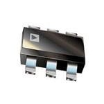
ICGOO电子元器件商城为您提供AD5246BKSZ100-RL7由Analog设计生产,在icgoo商城现货销售,并且可以通过原厂、代理商等渠道进行代购。 AD5246BKSZ100-RL7价格参考¥15.88-¥15.88。AnalogAD5246BKSZ100-RL7封装/规格:数据采集 - 数字电位器, Digital Potentiometer 100k Ohm 1 Circuit 128 Taps I²C Interface SC-70-6。您可以下载AD5246BKSZ100-RL7参考资料、Datasheet数据手册功能说明书,资料中有AD5246BKSZ100-RL7 详细功能的应用电路图电压和使用方法及教程。
AD5246BKSZ100-RL7是Analog Devices Inc.生产的一款数字电位器,属于数据采集类器件。该型号为128位分辨率的I²C接口数字电位器,阻值为100kΩ,采用SC70-6小型封装,适用于对空间要求严苛的便携式设备。

其主要应用场景包括:
1. 便携式电子设备:如智能手机、平板电脑和可穿戴设备中,用于LCD亮度调节、音频音量控制等,凭借小封装和低功耗特性,非常适合电池供电系统。
2. 工业控制与传感器调理:在传感器信号调理电路中,用于增益调节或偏置电压调整,提升系统精度与灵活性。
3. 电源管理:配合DC-DC转换器或稳压器,实现可编程输出电压控制,提高电源系统的适应性。
4. 医疗电子设备:如便携式监护仪,用于校准和微调模拟电路参数,确保测量准确性。
5. 消费类电子产品:如数码相机、音频设备中的自动增益控制或滤波器调节。

AD5246BKSZ100-RL7支持热切换和I²C总线通信,具备良好的稳定性和可靠性,适合需要远程或自动调节电阻值的场合。其工业级温度范围(-40°C 至 +125°C)也增强了在复杂环境下的适用性。总之,该器件广泛应用于需精密、可编程电阻调节的中小型电子系统中。
| 参数 | 数值 |
| 产品目录 | 集成电路 (IC)半导体 |
| 描述 | IC DGTL RES 100K I2C SC70-6数字电位计 IC IC 7-Bit I2C Dig Trimmer |
| DevelopmentKit | EVAL-AD5246DBZ |
| 产品分类 | |
| 品牌 | Analog Devices Inc |
| 产品手册 | |
| 产品图片 |
|
| rohs | 符合RoHS无铅 / 符合限制有害物质指令(RoHS)规范要求 |
| 产品系列 | 数字电位计 IC,Analog Devices AD5246BKSZ100-RL7- |
| 数据手册 | |
| 产品型号 | AD5246BKSZ100-RL7 |
| POT数量 | Single |
| 产品目录页面 | |
| 产品种类 | 数字电位计 IC |
| 供应商器件封装 | SC-70-6 |
| 其它名称 | AD5246BKSZ100RLCT |
| 包装 | 剪切带 (CT) |
| 商标 | Analog Devices |
| 存储器类型 | 易失 |
| 安装类型 | 表面贴装 |
| 安装风格 | SMD/SMT |
| 容差 | 30 % |
| 封装 | Reel |
| 封装/外壳 | 6-TSSOP,SC-88,SOT-363 |
| 封装/箱体 | SC70-6 |
| 工作温度 | -40°C ~ 125°C |
| 工作电源电压 | 5.5 V |
| 工厂包装数量 | 3000 |
| 弧刷存储器 | Volatile |
| 抽头 | 128 |
| 接口 | I²C |
| 数字接口 | I2C |
| 最大工作温度 | + 125 C |
| 最小工作温度 | - 40 C |
| 标准包装 | 1 |
| 每POT分接头 | 128 |
| 温度系数 | 标准值 45 ppm/°C |
| 电压-电源 | 2.7 V ~ 5.5 V |
| 电源电压-最大 | 5.5 V |
| 电源电压-最小 | 2.7 V |
| 电源电流 | 3 uA |
| 电路数 | 1 |
| 电阻 | 100 kOhms |
| 电阻(Ω) | 100k |
| 系列 | AD5246 |


- 商务部:美国ITC正式对集成电路等产品启动337调查
- 曝三星4nm工艺存在良率问题 高通将骁龙8 Gen1或转产台积电
- 太阳诱电将投资9.5亿元在常州建新厂生产MLCC 预计2023年完工
- 英特尔发布欧洲新工厂建设计划 深化IDM 2.0 战略
- 台积电先进制程称霸业界 有大客户加持明年业绩稳了
- 达到5530亿美元!SIA预计今年全球半导体销售额将创下新高
- 英特尔拟将自动驾驶子公司Mobileye上市 估值或超500亿美元
- 三星加码芯片和SET,合并消费电子和移动部门,撤换高东真等 CEO
- 三星电子宣布重大人事变动 还合并消费电子和移动部门
- 海关总署:前11个月进口集成电路产品价值2.52万亿元 增长14.8%


PDF Datasheet 数据手册内容提取
128-Position I2C-Compatible Digital Resistor Data Sheet AD5246 FEATURES FUNCTIONAL BLOCK DIAGRAM 128-position VDD End-to-end resistance 5 kΩ, 10 kΩ, 50 kΩ, 100 kΩ Ultracompact SC70-6 (2 mm × 2.1 mm) package SCL I2C® compatible interface I2C INTERFACE A SDA Full read/write of wiper register W Power-on preset to midscale Single supply 2.7 V to 5.5 V WIPER B Rheostat mode temperature coefficient: 45 ppm/°C REGISTER Low power, I = 0.9 µA at 3.3 V typical DD W ide operating temperature –40°C to +125°C GND 03875-001 Figure 1. APPLICATIONS Mechanical potentiometer replacement in new designs Transducer adjustment of pressure, temperature, position, chemical, and optical sensors RF amplifier biasing Automotive electronics adjustment Gain control and offset adjustment GENERAL OVERVIEW The AD5246 provides a compact 2 mm × 2.1 mm packaged solution for 128-position adjustment applications. This device performs the same electronic adjustment function as a variable resistor. Available in four different end-to-end resistance values (5 kΩ, 10 kΩ, 50 kΩ, 100 kΩ), these low temperature coefficient devices are ideal for high accuracy and stability variable resistance adjustments. The wiper settings are controllable through the I2C compatible digital interface, which can also be used to read back the present wiper register control word. The resistance between the wiper and either end point of the fixed resistor varies linearly with respect to the digital code transferred into the RDAC1 latch. Operating from a 2.7 V to 5.5 V power supply and consuming 0.9 µA (3.3 V) allows for usage in portable battery-operated applications. 1 The terms digital potentiometer, VR, and RDAC are used interchangeably in this document. Rev. C Information furnished by Analog Devices is believed to be accurate and reliable. However, no responsibility is assumed by Analog Devices for its use, nor for any infringements of patents or other rights of third parties that may result from its use. One Technology Way, P.O. Box 9106, Norwood, MA 02062-9106, U.S.A. Specifications subject to change without notice. No license is granted by implication or otherwise under any patent or patent rights of Analog Devices. Trademarks and Tel: 781.329.4700 www.analog.com registered trademarks are the property of their respective owners. Fax: 781.461.3113© 2003–2012 Analog Devices, Inc. All rights reserved.
AD5246 Data Sheet TABLE OF CONTENTS Specifications ..................................................................................... 3 Programming the Variable Resistor ......................................... 13 Electrical Characteristics—5 kΩ Version .................................. 3 I2C Compatible 2-Wire Serial Bus ........................................... 13 Electrical Characteristics—10 kΩ, 50 kΩ, 100 kΩ Versions .. 4 Level Shifting for Bidirectional Interface ................................ 14 Timing Characteristics ................................................................ 5 ESD Protection ........................................................................... 14 Absolute Maximum Ratings ............................................................ 6 Terminal Voltage Operating Range ......................................... 14 ESD CAUTION ............................................................................ 6 Maximum Operating Current .................................................. 14 Pin Configuration and Function Descriptions ............................. 7 Power-Up Sequence ................................................................... 14 Typical Performance Characteristics ............................................. 8 Layout and Power Supply Bypassing ....................................... 15 Test Circuits ..................................................................................... 11 Constant Bias to Retain Resistance Setting ............................. 15 I2C Interface ..................................................................................... 12 Outline Dimensions ....................................................................... 16 Operation ......................................................................................... 13 Ordering Guide .......................................................................... 16 REVISION HISTORY 5/12—Rev. B to Rev. C Changes to Features and General Description Sections .............. 1 Changes to I Parameters, Table 1 ................................................ 3 DD Changes to I Parameters, Table 2 ................................................ 4 DD Changes to Figure 10 ........................................................................ 9 Removed Evaluation Board Section ............................................. 15 Changes to Ordering Guide .......................................................... 16 8/09—Rev. A to Rev. B Changes to Power Supply Sensitivity Parameter .......................... 3 Updated Outline Dimensions ........................................................ 16 Changes to Ordering Guide ........................................................... 16 7/05—Rev. 0 to Rev. A Changes to Table 1 ............................................................................ 3 Changes to Table 2 ............................................................................ 4 Changes to Absolute Maximum Ratings ....................................... 6 Moved Pin Configuration and Function Descriptions ................ 7 Deleted Table 7 ................................................................................ 12 Changes to Operation Section ....................................................... 13 Deleted Figure 31 ............................................................................. 14 Changes to Figure 30 and Figure 32 ............................................. 14 9/03—Revision 0: Initial Version Rev. C | Page 2 of 16
Data Sheet AD5246 SPECIFICATIONS ELECTRICAL CHARACTERISTICS—5 kΩ VERSION V = 5 V ± 10% or 3 V ± 10%; V = +V ; –40°C < T < +125°C, unless otherwise noted. DD A DD A Table 1. Parameter Symbol Conditions Min Typ1 Max Unit DC CHARACTERISTICS—RHEOSTAT MODE Resistor Differential Nonlinearity2 R-DNL R –1.5 ±0.1 +1.5 LSB WB Resistor Integral Nonlinearity2 R-INL R –4 ±0.75 +4 LSB WB Nominal Resistor Tolerance3 ∆R T = 25°C –30 +30 % AB A Resistance Temperature Coefficient (∆R /R )/∆T Wiper = no connect 45 ppm/°C AB AB R R Code = 0x00, V = 5 V 75 150 Ω WB WB DD Code = 0x00, V = 2.7 V 150 400 Ω DD RESISTOR TERMINALS Voltage Range4 V GND V V B, W DD Capacitance5 B C f = 1 MHz, measured to GND, code = 0x40 45 pF B Capacitance5 W C f = 1 MHz, measured to GND, code = 0x40 60 pF W Common-Mode Leakage I 1 nA CM DIGITAL INPUTS AND OUTPUTS Input Logic High V V = 5 V 2.4 V IH DD Input Logic Low V V = 5 V 0.8 V IL DD Input Logic High V V = 3 V 2.1 V IH DD Input Logic Low V V = 3 V 0.6 V IL DD Input Current I V = 0 V or 5 V ±1 µA IL IN Input Capacitance5 C 5 pF IL POWER SUPPLIES Power Supply Range V 2.7 5.5 V DD RANGE Supply Current IDD VDD = 5.5 V; VIH = VDD or VIL = GND 3 7 µA VDD = 5 V; VIH = VDD or VIL = GND 2.5 5.2 µA VDD = 3.3 V; VIH = VDD or VIL = GND 0.9 2 µA Power Dissipation6 P V = 5 V or V = 0 V, V = 5 V 40 µW DISS IH IL DD Power Supply Sensitivity PSSR V = +5 V ± 10%, code = midscale ±0.01 ±0.025 %/% DD DYNAMIC CHARACTERISTICS5, 7 Bandwidth –3 dB BW_5K R = 5 kΩ, code = 0x40 1.2 MHz AB Total Harmonic Distortion THD V = 1 V rms, V = 0 V, f = 1 kHz 0.05 % W A B V Settling Time t V = 5 V, ±1 LSB error band 1 µs W S A Resistor Noise Voltage Density e R = 2.5 kΩ, R = 0 Ω 6 nV/√Hz N_WB WB S 1 Typical specifications represent average readings at 25°C and VDD = 5 V. 2 Resistor position nonlinearity error R-INL is the deviation from an ideal value measured between the maximum resistance and the minimum resistance wiper positions. R-DNL measures the relative step change from ideal between successive tap positions. Parts are guaranteed monotonic. 3 Code = 0x7F. 4 Resistor Terminal A and Resistor Terminal W have no limitations on polarity with respect to each other. 5 Guaranteed by design; not subject to production test. 6 PDISS is calculated from (IDD × VDD). CMOS logic level inputs result in minimum power dissipation. 7 VDD = 5 V. Rev. C | Page 3 of 16
AD5246 Data Sheet ELECTRICAL CHARACTERISTICS—10 kΩ, 50 kΩ, 100 kΩ VERSIONS V = 5 V ± 10% or 3 V ± 10%; V = V ; –40°C < T < +125°C, unless otherwise noted. DD A DD A Table 2. Parameter Symbol Conditions Min Typ1 Max Unit DC CHARACTERISTICS, RHEOSTAT MODE Resistor Differential Nonlinearity2 R-DNL R , V = no connect –1 ±0.1 +1 LSB WB A Resistor Integral Nonlinearity2 R-INL R , V = no connect –2 ±0.25 +2 LSB WB A Nominal Resistor Tolerance3 ∆R T = 25°C –20 +20 % AB A Resistance Temperature Coefficient (∆R /R )/∆T Wiper = no connect 45 ppm/°C AB AB R R Code=0x00, V = 5 V 75 150 Ω WB WB DD Code=0x00, V = 2.7 V 150 400 Ω DD RESISTOR TERMINALS Voltage Range4 V GND V V B, W DD Capacitance5 B C f = 1 MHz, measured to GND, code = 0x40 45 pF B Capacitance5 W C f = 1 MHz, measured to GND, code = 0x40 60 pF W Common-Mode Leakage I 1 nA CM DIGITAL INPUTS AND OUTPUTS Input Logic High V V = 5 V 2.4 V IH DD Input Logic Low V V = 5 V 0.8 V IL DD Input Logic High V V = 3 V 2.1 V IH DD Input Logic Low V V = 3 V 0.6 V IL DD Input Current I V = 0 V or 5 V ±1 µA IL IN Input Capacitance5 C 5 pF IL POWER SUPPLIES Power Supply Range V 2.7 5.5 V DD RANGE Supply Current IDD VDD = 5.5 V; VIH = VDD or VIL = GND 3 7 µA VDD = 5 V; VIH = VDD or VIL = GND 2.5 5.2 µA VDD = 3.3 V; VIH = VDD or VIL = GND 0.9 2 µA Power Dissipation6 P V = 5 V or V = 0 V, V = 5 V 40 µW DISS IH IL DD Power Supply Sensitivity PSSR V = +5 V ± 10%, code = midscale ±0.01 ±0.02 %/% DD DYNAMIC CHARACTERISTICS5, 7 Bandwidth –3 dB BW R = 10 kΩ/50 kΩ/100 kΩ, code = 0x40 600/100/40 kHz AB Total Harmonic Distortion THD V = 1 V rms, f = 1 kHz, R = 10 kΩ 0.05 % W A AB V Settling Time (10 kΩ/50 kΩ/100 kΩ) t V = 5 V ±1 LSB error band 2 µs W S A Resistor Noise Voltage Density e R = 5 kΩ, R = 0 9 nV/√Hz N_WB WB S 1 Typical specifications represent average readings at 25°C and VDD = 5 V. 2 Resistor position nonlinearity error R-INL is the deviation from an ideal value measured between the maximum resistance and the minimum resistance wiper positions. R-DNL measures the relative step change from ideal between successive tap positions. Parts are guaranteed monotonic. 3 Code = 0x7F. 4 Resistor Terminal A and Resistor Terminal W have no limitations on polarity with respect to each other. 5 Guaranteed by design; not subject to production test. 6 PDISS is calculated from (IDD × VDD). CMOS logic level inputs result in minimum power dissipation. 7 All dynamic characteristics use VDD = 5 V. Rev. C | Page 4 of 16
Data Sheet AD5246 TIMING CHARACTERISTICS V = 5 V ± 10% or 3 V ± 10%; V = V ; –40°C < T < +125°C, unless otherwise noted. DD A DD A Table 3. Parameter Symbol Conditions Min Typ1 Max Unit I2C INTERFACE TIMING CHARACTERISTICS2, 3, 4 SCL Clock Frequency f 400 kHz SCL t Bus Free Time Between STOP and START t 1.3 µs BUF 1 t Hold Time (Repeated START) t After this period, the first clock pulse is HD;STA 2 generated 0.6 µs t Low Period of SCL Clock t 1.3 µs LOW 3 t High Period of SCL Clock t 0.6 50 µs HIGH 4 t Setup Time for Repeated START Condition t 0.6 µs SU;STA 5 t Data Hold Time t 0.9 µs HD;DAT 6 t Data Setup Time t 100 ns SU;DAT 7 t Fall Time of Both SDA and SCL Signals t 300 ns F 8 t Rise Time of Both SDA and SCL Signals t 300 ns R 9 t Setup Time for STOP Condition t 0.6 µs SU;STO 10 1 Typical specifications represent average readings at 25°C and VDD = 5 V. 2 Guaranteed by design; not subject to production test. 3 See timing diagrams (Figure 26, Figure 27, and Figure 28) for locations of measured values. 4 Specifications apply to all parts. Rev. C | Page 5 of 16
AD5246 Data Sheet ABSOLUTE MAXIMUM RATINGS T = 25°C, unless otherwise noted. A Table 4. Stresses above those listed under Absolute Maximum Ratings Parameter Value may cause permanent damage to the device. This is a stress VDD to GND –0.3 V to +7 V rating only; functional operation of the device at these or any VA, VW to GND VDD other conditions above those indicated in the operational Terminal Current, A–B, A–W, B–W section of this specification is not implied. Exposure to absolute Pulsed1 ±20 mA maximum rating conditions for extended periods may affect Continuous ±5 mA device reliability. Digital Inputs and Output Voltage to GND 0 V to V + 0.3 V DD Operating Temperature Range –40°C to +125°C Maximum Junction Temperature (T ) 150°C JMAX Storage Temperature –65°C to +150°C Lead Temperature (Soldering, 10 sec) 300°C Thermal Resistance2 θJA: SC70-6 340°C/W 1 Maximum terminal current is bounded by the maximum current handling of the switches, maximum power dissipation of the package, and maximum applied voltage across any two of the A, B, and W terminals at a given resistance. 2 Package power dissipation = (TJMAX − TA)/θJA. ESD CAUTION ESD (electrostatic discharge) sensitive device. Electrostatic charges as high as 4000 V readily accumulate on the human body and test equipment and can discharge without detection. Although this product features proprietary ESD protection circuitry, permanent damage may occur on devices subjected to high energy electrostatic discharges. Therefore, proper ESD precautions are recommended to avoid performance degradation or loss of functionality. Rev. C | Page 6 of 16
Data Sheet AD5246 PIN CONFIGURATION AND FUNCTION DESCRIPTIONS VDD 1 6 B AD5246 GND 2 TOP VIEW 5 W (Not to Scale) SCL 3 4 SDA 03875-018 Figure 2. Pin Configuration Table 5. Pin Function Descriptions Pin No. Mnemonic Description 1 V Positive Power Supply. DD 2 GND Digital Ground. 3 SCL Serial Clock Input. Positive edge triggered. 4 SDA Serial Data Input/Output. 5 W W Terminal. 6 B B Terminal. Rev. C | Page 7 of 16
AD5246 Data Sheet TYPICAL PERFORMANCE CHARACTERISTICS 1.0 0.5 0.8 TRAAB= =2 51°0CkΩ 0.4 –+4205°°CC VRDADB == 21.07kVΩ +85°C B)B) 0.6 VDD = 2.7V SB) 0.3 +125°C L (LSL (LS 0.4 NL (L 0.2 TA =–40°C,+25°C,+85°C,+125°C NN 0.2 D 0.1 RHEOSTAT MODE IRHEOSTAT MODE I –––000...4260 VDD = 5.5V RHEOSTAT MODE –––000...1032 ––01..80 03875-020 ––00..54 03875-023 0 16 32 48 64 80 96 112 128 0 16 32 48 64 80 96 112 128 CODE (Decimal) CODE (Decimal) Figure 3. R-INL vs. Code vs. Supply Voltages Figure 6. R-DNL vs. Code vs. Temperature 0.5 0 00..34 RTAA B= =2 51°0CkΩ B) –0.5 S L (LSB) 0.2 VDD = 2.7V L (LSB)ROR (L–1.0 VDD = 5.5V, VA = 5.5V N 0.1 NR RHEOSTAT MODE D –––000...3210 VDD = 5.5V RHEOSTAT MODE IFSE, FULL-SCALE E–––122...550 VDD = 2.7V, VA = 2.7V ––00..54 03875-021 –3.0 03875-024 0 16 32 48 64 80 96 112 128 –40 –25 –10 5 20 35 50 65 80 95 110 125 CODE (Decimal) TEMPERATURE (°C) Figure 4. R-DNL vs. Code vs. Supply Voltages Figure 7. Full-Scale Error vs. Temperature 1.0 1.50 0.8 TA =–40°C 0.6 TA = +85°C B) 1.25 B) LS LS 0.4 R ( 1.00 NL ( 0.2 RRO STAT MODE I –0.20 TA = +25°C TA = +125°C RO-SCALE E 00..5705 VDD = 5.5V, VA = 5.5V O –0.4 E RHE –––100...086 TTTTAAAA ==== –+++42810552°°°5CCC°C 03875-022 ZSE, Z 0.205 VDD = 2.7V, VA = 2.7V 03875-025 0 16 32 48 64 80 96 112 128 –40 –25 –10 5 20 35 50 65 80 95 110 125 CODE (Decimal) TEMPERATURE (°C) Figure 5. R-INL vs. Code vs. Temperature Figure 8. Zero-Scale Error vs. Temperature Rev. C | Page 8 of 16
Data Sheet AD5246 100 0 DIGITAL INPUTS = 0V –6 0x40 CODE = 0x40 0x20 –12 A) 10 0x10 µNT ( VDD = 5.5V –18 0x08 UPPLY CURRE 1 VDD = 2.7V GAIN (dB) –––233406 000xxx000421 S –42 D, 0.1 D I –48 0.01 03875-026 ––5640 03875-029 –40 –25 –10 5 20 35 50 65 80 95 110 125 1k 10k 100k 1M 10M TEMPERATURE (°C) FREQUENCY (Hz) Figure 9. Supply Current vs. Temperature Figure 12. Gain vs. Frequency vs. Code, RAB = 10 kΩ 100 5V IWB = 200µA 0 C) 90 2.7V RAB = 10kΩ –6 0x40 pm/° 80 –12 0x20 p CO ( 70 –18 0x10 P DE TEM 5600 N (dB) ––2340 00xx0048 O AI T M 40 G –36 0x02 A T 0x01 OS 30 –42 S HE 20 –48 T R 1001 9 17 25 33 41 4C9O5D7E (6D5ec7im3al8)1 89 97 105113121 03875-027 ––56401k 10k FREQU1E00NkCY (Hz) 1M 10M03875-030 Figure 10. Rheostat Mode Tempco ∆RWB/∆T vs. Code Figure 13. Gain vs. Frequency vs. Code, RAB = 50 kΩ 0 0 0x40 –6 0x40 –6 0x20 –12 0x20 –12 0x10 –18 0x10 –18 0x08 dB) –24 0x04 B) –24 0x08 GAIN ( ––3306 00xx0021 GAIN (d –30 00xx0042 –36 –42 0x01 –42 –48 –48 ––56401k 10k 100k 1M 10M03875-028 ––5640 03875-031 1k 10k 100k 1M 10M FREQUENCY (Hz) FREQUENCY (Hz) Figure 11. Gain vs. Frequency vs. Code, RAB = 5 kΩ Figure 14. Gain vs. Frequency vs. Code, RAB = 100 kΩ Rev. C | Page 9 of 16
AD5246 Data Sheet 0 VDD = 5.5V TA = 25°C –6 VB = 0V RAB = 10kΩ 5kΩ FCLK = 100kHz –12 10kΩ –18 100kΩ 50kΩ VW B) –24 d N ( –30 AI G –36 5V –42 CLK 0V –48 ––56401k 10k 100k 1M 10M03875-032 1µs/DIV 03875-006 FREQUENCY (Hz) Figure 15. –3 dB Bandwidth @ Code = 0x80 Figure 18. Digital Feedthrough 0.30 A - CVODDD E= =5 .05xV55 TA= 25°C VCVDBOD D= =E0 V50.x54V0 to 0x3F RTAA B= =2 51°0CkΩ 0.25 B - VDD = 5.5V CODE = 0x7F 0.20 C - VDD = 2.7V CODE = 0x55 µ(A)0.15 D - CVODDD E= =2 .07xV7F D ID VW 0.10 A B 0.05 0 CD 03875-033 03875-007 1k 10k 100k 1M 200ns/DIV FREQUENCY (Hz) Figure 16. IDD vs. Frequency Figure 19. Midscale Glitch, Code 0x40 to 0x3F 360 RTAA B= =2 55°0CkΩ VVDBD = =0 V5.5V RATBA == 1205k°ΩC 300 CODE = 0x00 CODE 00H TO 7FH IW = 50µA VDD = 2.7V 240 Ω) (B 180 W R VW 1 120 VDD = 5.5V 600 03875-008 40µs/DIV 03875-005 0 0.5 1.0 1.5 2.0 2.5 3.0 3.5 4.0 4.5 5.0 5.5 VBIAS (V) Figure 17. RWB vs. VBIAS vs. VDD Figure 20. Large Signal Settling Time Rev. C | Page 10 of 16
Data Sheet AD5246 TEST CIRCUITS Figure 21 to Figure 25 define the test conditions used in the product Specification tables. 0.1V DUT DUT RSW= ISW IW CODE = 0x00 W W B B ISW 0.1V VMS 03875-004 VDD TO GND 03875-040 Figure 21. Test Circuit for Resistor Position Nonlinearity Error Figure 24. Test Circuit for Incremental On Resistance (Rheostat Operation; R-INL, R-DNL) DUT V+ VDD BDUWT VMPPVS+SS RS= RV(% D(dD/%B±))1 ==0 %2∆∆0VV LMDODS%%G( ∆∆ VV MD DS ) 03875-009 NO CONBNWECT IVCCMM 03875-012 Figure 22. Test Circuit for Power Supply Sensitivity (PSS, PSSR) Figure 25. Test Circuit for Common-Mode Leakage Current 10kΩ DUT 10kΩ +15V VIN W B OP27 VOUT 2.5V –15V 03875-010 Figure 23. Test Circuit for Gain vs. Frequency Rev. C | Page 11 of 16
AD5246 Data Sheet I2C INTERFACE Table 6. Write Mode S 0 1 0 1 1 1 0 W A X D6 D5 D4 D3 D2 D1 D0 A P Slave Address Byte Data Byte Table 7. Read Mode S 0 1 0 1 1 1 0 R A 0 D6 D5 D4 D3 D2 D1 D0 A P Slave Address Byte Data Byte S = Start Condition. W = Write. P = Stop Condition. R = Read. A = Acknowledge. D6, D5, D4, D3, D2, D1, D0 = Data Bits. X = Don’t Care. t8 t9 t2 SCL t6 t2 t3 t4 t7 t5 t10 t9 t8 SDA P t1 S S P 03875-019 Figure 26. I2C Interface, Detailed Timing Diagram 1 9 1 9 1 SCL SDA 0 1 0 1 1 1 0 R/W X D6 D5 D4 D3 D2 D1 D0 SMTAASRTTE BRY SLAVE AFRDADMREES 1S BYTE AACDK52 B46Y DAFRTAA MBEY T2E AACDK52 B46Y SMTAOSPT EBRY 03875-014 Figure 27. Writing to the RDAC Register 1 9 1 9 SCL SDA 0 1 0 1 1 1 0 R/W 0 D6 D5 D4 D3 D2 D1 D0 SMTAASRTTE BRY SLAVE FARDADMREE S1S BYTE AACDK52 B46Y RDAFCR RAEMGEI S2TER NBOY MACAKSTSMETRAOSPT EBRY 03875-013 Figure 28. Reading from the RDAC Register Rev. C | Page 12 of 16
Data Sheet AD5246 OPERATION The AD5246 is a 128-position, digitally controlled variable I2C COMPATIBLE 2-WIRE SERIAL BUS resistor (VR) device. The first byte of the AD5246 is a slave address byte (see Table 6 PROGRAMMING THE VARIABLE RESISTOR and Table 7). It has a 7-bit slave address and an R/W bit. The Rheostat Operation seven MSBs of the slave address are 0101110 followed by 0 for a write command or 1 to place the device in read mode. The nominal resistance of the RDAC between Terminal A and Terminal B is available in 5 kΩ, 10 kΩ, 50 kΩ, and 100 kΩ. The 2-wire I2C serial bus protocol operates as follows: The final two or three digits of the part number determine the nominal resistance value, that is, 10 kΩ = 10, 50 kΩ = 50. 1. The master initiates data transfer by establishing a START The nominal resistance (R ) of the VR has 128 contact points condition, which is when a high-to-low transition on the AB accessed by the wiper terminal. The 7-bit data in the RDAC SDA line occurs while SCL is high (see Figure 27). The latch is decoded to select one of the 128 possible settings. following byte is the slave address byte, which consists of the 7-bit slave address followed by an R/W bit (this bit The general equation determining the digitally programmed determines whether data will be read from or written to output resistance between W and B is the slave device). D R (D)= ×R +2×R (1) The slave whose address corresponds to the transmitted WB 128 AB W address responds by pulling the SDA line low during the ninth clock pulse (this is termed the acknowledge bit). where: At this stage, all other devices on the bus remain idle while D is the decimal equivalent of the binary code loaded in the the selected device waits for data to be written to or read 7-bit RDAC register. from its serial register. If the R/W bit is high, the master RAB is the end-to-end resistance. reads from the slave device. Conversely, if the R/W bit is RW is the wiper resistance contributed by the on resistance low, the master writes to the slave device. of each internal switch. 2. In write mode, after acknowledgement of the slave address Ax byte, the next byte is the data byte. Data is transmitted over the serial bus in sequences of nine clock pulses (eight data bits followed by an acknowledge bit). The transitions on DD65 RS the SDA line must occur during the low period of SCL and D4 D3 remain stable during the high period of SCL (see Table 6). DD21 RS D0 Wx 3. In read mode, after acknowledgment of the slave address byte, data is received over the serial bus in sequences of RDAC nine clock pulses (a slight difference from the write mode LATCH where eight data bits are followed by an acknowledge bit). DECAONDDER RS Bx Similarly, the transitions on the SDA line must occur 03875-015 dthuer ihnigg hth pee lroiowd p oefr iSoCdL o (fs SeCe LFi agnudre r 2em8)a. in stable during Figure 29. AD5246 Equivalent RDAC Circuit 4. When all data bits have been read or written, a STOP condition is established by the master. A STOP condition Note that in the zero-scale condition, there is a relatively small is defined as a low-to-high transition on the SDA line while finite wiper resistance. Care should be taken to limit the current SCL is high. In write mode, the master pulls the SDA line flow between W and B in this state to a maximum pulse current high during the tenth clock pulse to establish a STOP of no more than 20 mA. Otherwise, degradation or possible condition (see Figure 27). In read mode, the master issues destruction of the internal switch contact can occur. a No Acknowledge for the ninth clock pulse (that is, the SDA line remains high). The master then brings the SDA Typical device-to-device matching is process lot dependent and line low before the tenth clock pulse, which goes high to may vary by up to ±30%. Since the resistance element is proc- establish a STOP condition (see Figure 28). essed in thin-film technology, the temperature coefficient of R is only 45 ppm/°C. AB Rev. C | Page 13 of 16
AD5246 Data Sheet A repeated write function gives the user flexibility to update the VDD RDAC output a number of times after addressing the part only once. For example, after the RDAC has acknowledged its slave B address in write mode, the RDAC output updates on each succes- sive byte. If different instructions are needed, the write/read mode W has to start again with a new slave address and data byte. LSiEmVilEarLly S, aH rIeFpTeaItNedG r eFaOd fRu nBcItDioInR oEf CthTeI RODNAACL i sI NalsToE aRlloFwAeCd.E GND 03875-016 While most legacy systems may be operated at one voltage, Figure 32. Maximum Terminal Voltages Set by VDD and GND a new component may be optimized at another. When two systems operate the same signal at two different voltages, proper MAXIMUM OPERATING CURRENT level shifting is needed. For instance, one can use a 1.8 V At low code values, the user should be aware that due to low E2PROM to interface with a 5 V digital potentiometer. A level resistance values, the current through the RDAC may exceed shifting scheme is needed to enable a bidirectional communi- the 5 mA limit. In Figure 33, a 5 V supply is placed on the cation so that the setting of the digital potentiometer can be wiper, and the current through Terminal W and Terminal B is stored to and retrieved from the E2PROM. Figure 30 shows plotted with respect to code. A line is also drawn denoting the one of the implementations. M1 and M2 can be any N channel 5 mA current limit. Note that at low code values (particularly signal FETs, or if V falls below 2.5 V, M1 and M2 can be low DD for the 5 kΩ and 10 kΩ options), the current level increases threshold FETs such as the FDV301N. significantly. Care should be taken to limit the current flow between W and B in this state to a maximum continuous current of 5 mA and a maximum pulse current of no more than VDD1= 1.8V VDD2=5V 20 mA. Otherwise, degradation or possible destruction of the RP RP RP RP internal switch contacts can occur. G SDA1 S D SDA2 G 100 M1 SCL1 S D SCL2 M2 1.8V 5V 10 5mA CURRENT LIMIT E2PROM AD5246 03875-011 NT (mA) RAB= 5kΩ Figure 30. Level Shifting for Operation at Different Potentials RRE 1 CU RAB= 10kΩ B W RAB= 50kΩ I ESD PROTECTION 0.1 Aanlld d pigaritaalll eiln Zpuentse ar rEeS pDro sttercutcetdu rweist,h a as ssheroiwesn i ninp uFti gruesries t3o1r. 0.01 RAB= 100kΩ 03875-034 This applies to the digital input pins SDA and SCL. 0 16 32 48 64 80 96 112 128 CODE (Decimal) Figure 33. Maximum Operating Current 340Ω LOGIC 03875-002 POWER-UP SEQUENCE GND Since the ESD protection diodes limit the voltage compliance at Terminal B and Terminal W (see Figure 32), it is important Figure 31. ESD Protection of Digital Pins to power V /GND before applying any voltage to Terminal B DD and Terminal W; otherwise, the diode is forward biased such TERMINAL VOLTAGE OPERATING RANGE that V is powered unintentionally and may affect the rest of DD The AD5246 V and GND power supply defines the boundary the user’s circuit. The ideal power-up sequence is in the follow- DD conditions for proper 3-terminal digital potentiometer ing order: GND, VDD, digital inputs, and then VB/VW. The operation. Supply signals present on Terminal B and relative order of powering VB and VW and the digital inputs Terminal W that exceed VDD or GND are clamped by is not important, providing they are powered after VDD/GND. the internal forward biased diodes (see Figure 32). Rev. C | Page 14 of 16
Data Sheet AD5246 LAYOUT AND POWER SUPPLY BYPASSING The measurement over time shows that the device draws approximately 1.3 µA and consumes negligible power. Over It is a good practice to use a compact, minimum lead-length a course of 30 days, the battery was depleted by less than 2%, layout design. The leads to the inputs should be as direct as the majority of which is due to the intrinsic leakage current possible with a minimum conductor length. Ground paths of the battery itself. should have low resistance and low inductance. Similarly, it is good practice to bypass the power supplies with quality capacitors for optimum stability. Supply leads to the 110% device should be bypassed with 0.01 µF to 0.1 µF disc or chip 108% ceramic capacitors. Low ESR 1 µF to 10 µF tantalum or TA= 25°C 106% electrolytic capacitors should also be applied at the supplies to D E104% minimize any transient disturbance and low frequency ripple T E (see Figure 34). Note that the digital ground should also be PL102% E D joined remotely to the analog ground at one point to minimize E 100% F the ground bounce. Y LI 98% R E TT 96% A B 94% VDDC3 +10µFC1 0.1µF VDDAD5246 9902%% 03875-035 0 5 10 15 20 25 30 DAYS Figure 35. Battery Operating Life Depletion GND 03875-017 This demonstrates that constantly biasing the pot is not an Figure 34. Power Supply Bypassing impractical approach. Most portable devices do not require the removal of batteries for the purpose of charging. Although the CONSTANT BIAS TO RETAIN RESISTANCE SETTING resistance setting of the AD5246 will be lost when the battery For users who desire nonvolatility but cannot justify the addi- needs replacement, such events occur rather infrequently, so tional cost for the EEMEM, the AD5246 may be considered as that this inconvenience is justified by the lower cost and smaller a low cost alternative by maintaining a constant bias to retain size offered by the AD5246. If and when total power is lost, the wiper setting. The AD5246 was designed specifically with the user should be provided with a means to adjust the setting low power in mind, which allows low power consumption accordingly. even in battery-operated systems. The graph in Figure 35 demonstrates the power consumption from a 3.4 V 450 mA/hr Li-ion cell phone battery, which is connected to the AD5246. Rev. C | Page 15 of 16
AD5246 Data Sheet OUTLINE DIMENSIONS 2.20 2.00 1.80 1.35 6 5 4 2.40 1.25 2.10 1.15 1 2 3 1.80 0.65BSC 1.30BSC 1.00 1.10 0.40 0.90 0.80 0.10 0.70 0.46 0.10MAX 0.30 SPELAATNIENG 00..2028 0.36 COPLANARITY 0.15 0.26 0.10 COMPLIANTTOJEDECSTANDARDSMO-203-AB 072809-A Figure 36. 6-Lead Thin Shrink Small Outline Transistor Package [SC70] (KS-6) Dimensions shown in millimeters ORDERING GUIDE Model1, 2 R (kΩ) Temperature Range Package Description Package Option Branding AB AD5246BKSZ5-RL7 5 –40°C to +125°C 6-lead SC70 KS-6 D93 AD5246BKSZ10-R2 10 –40°C to +125°C 6-lead SC70 KS-6 D92 AD5246BKSZ10-RL7 10 –40°C to +125°C 6-lead SC70 KS-6 D92 AD5246BKSZ50-RL7 50 –40°C to +125°C 6-lead SC70 KS-6 D94 AD5246BKSZ100-R2 100 –40°C to +125°C 6-lead SC70 KS-6 D9D AD5246BKSZ100-RL7 100 –40°C to +125°C 6-lead SC70 KS-6 D9D EVAL-AD5246DBZ Evaluation Board 1 Z = RoHS Compliant Part. 2 The evaluation board is shipped with the 10 kΩ RAB resistor option; however, the board is compatible with all available resistor value options. Purchase of licensed I2C components of Analog Devices or one of its sublicensed Associated Companies conveys a license for the purchaser under the Philips I2C Patent Rights to use these components in an I2C system, provided that the system conforms to the I2C Standard Specification as defined by Philips. © 2003–2012 Analog Devices, Inc. All rights reserved. Trademarks and registered trademarks are the property of their respective owners. D03875–0–5/12(C) Rev. C | Page 16 of 16
Mouser Electronics Authorized Distributor Click to View Pricing, Inventory, Delivery & Lifecycle Information: A nalog Devices Inc.: AD5246BKSZ100-R2