ICGOO在线商城 > 集成电路(IC) > 数据采集 - 数字电位器 > AD5228BUJZ10-RL7
 Datasheet下载
- 型号: AD5228BUJZ10-RL7
- 制造商: Analog
- 库位|库存: xxxx|xxxx
- 要求:
| 数量阶梯 | 香港交货 | 国内含税 |
| +xxxx | $xxxx | ¥xxxx |
查看当月历史价格
查看今年历史价格
AD5228BUJZ10-RL7产品简介:
ICGOO电子元器件商城为您提供AD5228BUJZ10-RL7由Analog设计生产,在icgoo商城现货销售,并且可以通过原厂、代理商等渠道进行代购。 AD5228BUJZ10-RL7价格参考¥4.10-¥10.17。AnalogAD5228BUJZ10-RL7封装/规格:数据采集 - 数字电位器, Digital Potentiometer 10k Ohm 1 Circuit 32 Taps Pushbutton Interface TSOT-23-8。您可以下载AD5228BUJZ10-RL7参考资料、Datasheet数据手册功能说明书,资料中有AD5228BUJZ10-RL7 详细功能的应用电路图电压和使用方法及教程。
AD5228BUJZ10-RL7 是由 Analog Devices Inc. 生产的一款数字电位器,属于数据采集系统的一部分。该器件具有两个独立的、非易失性(NV)数字电位器通道,每个通道有 10,000 欧姆的标称阻值。它广泛应用于需要精确电阻调节和存储设置的应用场景中。

 应用场景:

1. 自动测试设备 (ATE):
   在自动测试设备中,AD5228BUJZ10-RL7 可用于精确调整测量电路中的电阻值,确保测试结果的准确性。其非易失性存储功能允许在断电后保存当前设置,从而减少重新校准的时间和成本。

2. 工业控制系统:
   工业自动化系统中,该数字电位器可以用于调节传感器或执行器的增益、偏置电压等参数。例如,在温度控制回路中,它可以动态调整反馈电阻,以适应不同的工作条件,确保系统的稳定性和精度。

3. 医疗设备:
   医疗仪器如监护仪、超声波设备等对精度要求极高。AD5228BUJZ10-RL7 可用于这些设备的信号调理电路中,提供高精度的电阻调节,确保测量数据的准确性,并且可以通过软件进行远程配置,提高设备的灵活性和可靠性。

4. 音频设备:
   在音频处理设备中,如混音台、功放等,该器件可用于音量控制、均衡器调节等场合。其数字控制特性使得用户可以通过软件界面方便地调整音效参数,同时保持高分辨率和稳定性。

5. 通信设备:
   通信系统中,AD5228BUJZ10-RL7 可用于调节滤波器、放大器等关键组件的参数。它能够通过 I²C 接口与微控制器通信,实现远程配置和监控,确保通信链路的最佳性能。

6. 消费电子产品:
   在一些高端消费电子产品中,如智能家居控制器、便携式音频设备等,该数字电位器可以用于用户界面的个性化设置,如亮度调节、对比度调整等,提升用户体验。

总之,AD5228BUJZ10-RL7 凭借其高精度、非易失性和易于集成的特点,适用于多种需要灵活电阻调节的应用领域,尤其适合那些对可靠性和精度有较高要求的场合。
| 参数 | 数值 |
| 产品目录 | 集成电路 (IC)半导体 |
| 描述 | IC DGTL POT UP/DN 10K TSOT23-8数字电位计 IC IC 5-Bit PB Up/Down |
| DevelopmentKit | EVAL-AD5228EBZ |
| 产品分类 | |
| 品牌 | Analog Devices |
| 产品手册 | |
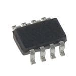
| 产品图片 |
|
| rohs | 符合RoHS无铅 / 符合限制有害物质指令(RoHS)规范要求 |
| 产品系列 | 数字电位计 IC,Analog Devices AD5228BUJZ10-RL7- |
| 数据手册 | |
| 产品型号 | AD5228BUJZ10-RL7 |
| PCN过时产品 | |
| POT数量 | Single |
| 产品目录页面 | |
| 产品种类 | 数字电位计 IC |
| 供应商器件封装 | TSOT-23-8 |
| 其它名称 | AD5228BUJZ10RL7DKR |
| 包装 | Digi-Reel® |
| 商标 | Analog Devices |
| 存储器类型 | 易失 |
| 安装类型 | 表面贴装 |
| 安装风格 | SMD/SMT |
| 容差 | 20 % |
| 封装 | Reel |
| 封装/外壳 | SOT-23-8 薄型,TSOT-23-8 |
| 封装/箱体 | TSOT-8 |
| 工作温度 | -40°C ~ 105°C |
| 工作电源电压 | 2.7 V |
| 工厂包装数量 | 3000 |
| 弧刷存储器 | Volatile |
| 抽头 | 32 |
| 接口 | 2 线按钮 |
| 数字接口 | Push Button |
| 最大工作温度 | + 105 C |
| 最小工作温度 | - 40 C |
| 标准包装 | 1 |
| 每POT分接头 | 32 |
| 温度系数 | 35 PPM / C |
| 电压-电源 | 2.7 V ~ 5.5 V |
| 电源电压-最大 | 5.5 V |
| 电源电压-最小 | 2.7 V |
| 电源电流 | 0.4 uA |
| 电路数 | 1 |
| 电阻 | 10 kOhms |
| 电阻(Ω) | 10k |
| 系列 | AD5228 |
| 配用 | /product-detail/zh/EVAL-AD5228EBZ/EVAL-AD5228EBZ-ND/1649690 |


- 商务部:美国ITC正式对集成电路等产品启动337调查
- 曝三星4nm工艺存在良率问题 高通将骁龙8 Gen1或转产台积电
- 太阳诱电将投资9.5亿元在常州建新厂生产MLCC 预计2023年完工
- 英特尔发布欧洲新工厂建设计划 深化IDM 2.0 战略
- 台积电先进制程称霸业界 有大客户加持明年业绩稳了
- 达到5530亿美元!SIA预计今年全球半导体销售额将创下新高
- 英特尔拟将自动驾驶子公司Mobileye上市 估值或超500亿美元
- 三星加码芯片和SET,合并消费电子和移动部门,撤换高东真等 CEO
- 三星电子宣布重大人事变动 还合并消费电子和移动部门
- 海关总署:前11个月进口集成电路产品价值2.52万亿元 增长14.8%


PDF Datasheet 数据手册内容提取
32-Position Manual Up/Down Control Potentiometer Data Sheet AD5228 FEATURES FUNCTIONAL BLOCK DIAGRAM 32-position digital potentiometer 10 kΩ, 50 kΩ, 100 kΩ end-to-end terminal resistance UP/DOWN D AD5228 Simple manual up/down control VDD COLONTGRICOL CE O Self-contained, requires only 2 pushbutton tactile switches D A R1 R2 E Built-in adaptive debouncer DISCRETE W Discrete step-up/step-down control STEP/AUTO Autoscan up/down control with 4 steps per second SCAN DETECT B PUSH-UP Pin-selectable zero-scale/midscale preset BUTTON PU Low potentiometer mode tempco, 5 ppm/°C ADAPTIVE ZERO- OR MID- LDoigwi trahle coosnttarto ml coodmep taetmibpleco , 35 ppm/°C PUBSUHT-TDOONWN PD DEBOUNCER SCALE PRESET 04422-0-001 Ultralow power, IDD = 0.4 µA typ and 3 µA max PRE GND Low operating voltage, 2.7 V to 5.5 V Temperature range, −40°C to +105°C Figure 1. Compact thin SOT-23-8 (2.9 mm × 3 mm) Pb-free package The AD5228 can increment or decrement the resistance in APPLICATIONS discrete steps or in autoscan mode. When the PU or PD button is pressed briefly (no longer than 0.6 s), the resistance of the Mechanical potentiometer and trimmer replacements LCD backlight, contrast, and brightness controls AD5228 changes by one step. When the PU or PD button is Digital volume control held continuously for more than a second, the device activates Portable device-level adjustments the autoscan mode and changes four resistance steps per Electronic front panel-level controls second. Programmable power supply The AD5228 can also be controlled digitally; its up/down features simplify microcontroller usage. The AD5228 is available GENERAL DESCRIPTION in a compact thin SOT-23-8 (TSOT-8) package. The part is The AD5228 is Analog Devices’ latest 32-step-up/step-down guaranteed to operate over the temperature range of −40°C to control digital potentiometer emulating mechanical potenti- +105°C. ometer operation1. Its simple up/down control interface allows The AD5228’s simple interface, small footprint, and very low manual control with just two external pushbutton tactile cost enable it to replace mechanical potentiometers and switches. The AD5228 is designed with a built-in adaptive trimmers with typically 3× improved resolution, solid-state debouncer that ignores invalid bounces due to contact bounce reliability, and faster adjustment, resulting in considerable cost commonly found in mechanical switches. The debouncer is saving in end users’ systems. adaptive, accommodating a variety of pushbutton tactile switches that generally have less than 10 ms of bounce time Users who consider EEMEM potentiometers should refer to the during contact closures. When choosing the switch, the user recommendations in the Applications section. should consult the timing specification of the switch to ensure Table 1. Truth Table its suitability in an AD5228 application. PU PD Operation1 0 0 R Decrement WB 0 1 R Increment WB 1 0 R Decrement WB 1 1 RWB Does Not Change 1RWA increments if RWB decrements and vice versa. 1 The terms digital potentiometer and RDAC are used interchangeably. Rev. B Document Feedback Information furnished by Analog Devices is believed to be accurate and reliable. However, no responsibility is assumed by Analog Devices for its use, nor for any infringements of patents or other One Technology Way, P.O. Box 9106, Norwood, MA 02062-9106, U.S.A. rights of third parties that may result from its use. Specifications subject to change without notice. No license is granted by implication or otherwise under any patent or patent rights of Analog Devices. Tel: 781.329.4700 ©2004–2015 Analog Devices, Inc. All rights reserved. Trademarks and registered trademarks are the property of their respective owners. Technical Support www.analog.com
AD5228 Data Sheet TABLE OF CONTENTS Features .............................................................................................. 1 Terminal Voltage Operation Range ......................................... 13 Applications ....................................................................................... 1 Power-Up and Power-Down Sequences .................................. 14 General Description ......................................................................... 1 Layout and Power Supply Biasing ............................................ 14 Revision History ............................................................................... 2 Applications ..................................................................................... 15 Electrical Characteristics ................................................................. 3 Manual Adjustable LED Driver ................................................ 15 Interface Timing Diagrams ......................................................... 4 Adjustable Current Source for LED Driver ............................ 15 Absolute Maximum Ratings ............................................................ 5 Adjustable High Power LED Driver ........................................ 15 ESD Caution .................................................................................. 5 Automatic LCD Panel Backlight Control ................................ 16 Pin Configuration and Function Descriptions ............................. 6 Audio Amplifier with Volume Control ................................... 16 Typical Performance Characteristics ............................................. 7 Constant Bias with Supply to Retain Resistance Setting ...... 17 Theory of Operation ...................................................................... 11 Outline Dimensions ....................................................................... 18 Programming the Digital Potentiometers ............................... 12 Ordering Guide .......................................................................... 18 Controlling Inputs ...................................................................... 13 REVISION HISTORY 6/15—Rev. A to Rev. B Changes to Features Section and General Description Section .... 1 Changes to Ordering Guide ........................................................... 18 4/09—Rev. 0 to Rev. A Changes to Table 2………………………………………………3 4/04—Revision 0: Initial Version Rev. B | Page 2 of 18
Data Sheet AD5228 ELECTRICAL CHARACTERISTICS 10 kΩ, 50 kΩ, 100 kΩ versions: V = 3 V ± 10% or 5 V ± 10%, V = V , V = 0 V, −40°C < T < +105°C, unless otherwise noted. DD A DD B A Table 2. Parameter Symbol Conditions Min Typ1 Max Unit DC CHARACTERISTICS, RHEOSTAT MODE Resistor Differential Nonlinearity2 R-DNL R , A terminal = no connect −0.5 ±0.05 +0.5 LSB WB Resistor Integral Nonlinearity2 R-INL R , A terminal = no connect −0.5 ±0.1 +0.5 LSB WB Nominal Resistor Tolerance3 ∆R /R −20 +20 % AB AB Resistance Temperature Coefficient (∆R /R ) × 104/∆T 35 ppm/°C AB AB Wiper Resistance R V = 2.7 V 100 250 Ω W DD V = 2.8 V to 5.5 V 50 200 Ω DD DC CHARACTERISTICS, POTENTIOMETER DIVIDER MODE (Specifications apply to all RDACs) Resolution N 5 Bits Integral Nonlinearity3 INL −0.5 ±0.05 +0.5 LSB Differential Nonlinearity3, 5 DNL −0.5 ±0.05 +0.5 LSB Voltage Divider Temperature Coefficient (∆V /V ) × 104/∆T Midscale 5 ppm/°C W W Full-Scale Error V ≥+15 steps from midscale −1 .2 −0.5 0 LSB WFSE Zero-Scale Error V ≤−16 steps from midscale 0 0.3 0.6 LSB WZSE RESISTOR TERMINALS Voltage Range6 V With respect to GND 0 V V A, B, W DD Capacitance4 A, B C f = 1 MHz, measured to GND 140 pF A, B Capacitance4 W C f = 1 MHz, measured to GND 150 pF W Common-Mode Leakage I V = V = V 1 nA CM A B W PU, PD INPUTS Input High V V = 5 V 2.4 5.5 V IH DD Input Low V V = 5 V 0 0.8 V IL DD Input Current I V = 0 V or 5 V ±1 μA I IN Input Capacitance4 C 5 pF I POWER SUPPLIES Power Supply Range V V = 5 V, PU = PD = V 2.7 5.5 V DD DD DD Supply Standby Current I 0.4 3 μA DD_STBY Supply Active Current7 I V = 5 V, PU or PD = 0 V 50 110 μA DD_ACT DD Power Dissipation7, 8 P V = 5 V 17 μW DISS DD Power Supply Sensitivity PSSR V = 5 V ± 10% 0.01 0.05 %/% DD Footnotes on next page. Rev. B | Page 3 of 18
AD5228 Data Sheet Parameter Symbol Conditions Min Typ1 Max Unit DYNAMIC CHARACTERISTICS 4, 9, 10, 11 Built-in Debounce and Settling Time 12 t 6 ms DB PU Low Pulse Width t 12 ms PU PD Low Pulse Width t 12 ms PD PU High Repetitive Pulse Width t 1 μs PU_REP PD High Repetitive Pulse Width t 1 μs PD_REP Autoscan Start Time t PU or PD = 0 V 0.6 0.8 1.2 s AS_START Autoscan Time t PU or PD = 0 V 0.16 0.25 0.38 s AS Bandwidth –3 dB BW_10 R = 10 kΩ, midscale 460 kHz AB BW_50 R = 50 kΩ, midscale 100 kHz AB BW_100 R = 100 kΩ, midscale 50 kHz AB Total Harmonic Distortion THD V = 1 V rms, R = 10 kΩ, 0.05 % A AB V = 0 V dc, f = 1 kHz B Resistor Noise Voltage eN_WB RWB = 5 kΩ, f = 1 kHz 14 nV/√Hz 1 Typicals represent average readings at 25°C, VDD = 5 V. 2 Resistor position nonlinearity error, R-INL, is the deviation from an ideal value measured between the maximum resistance and the minimum resistance wiper positions. R-DNL measures the relative step change from ideal between successive tap positions. Parts are guaranteed monotonic. 3 INL and DNL are measured at VW with the RDAC configured as a potentiometer divider similar to a voltage output D/A converter. VA = VDD and VB = 0 V. 4 Guaranteed by design and not subject to production test. 5 DNL specification limits of ±1 LSB maximum are guaranteed monotonic operating conditions. 6 Resistor Terminals A, B, and W have no limitations on polarity with respect to each other. 7 PU and PD have 100 kΩ internal pull-up resistors, IDD_ACT = VDD/100 kΩ + IOSC (internal oscillator operating current) when PU or PD is connected to ground. 8 PDISS is calculated based on IDD_STBY × VDD only. IDD_ACT duration should be short. Users should not hold PU or PD pin to ground longer than necessary to elevate power dissipation. 9 Bandwidth, noise, and settling time are dependent on the terminal resistance value chosen. The lowest R value results in the fastest settling time and highest bandwidth. The highest R value results in the minimum overall power consumption. 10 All dynamic characteristics use VDD = 5 V. 11 Note that all input control voltages are specified with tR = tF = 1 ns (10% to 90% of VDD) and timed from a voltage level of 1.6 V. Switching characteristics are measured using VDD = 5 V. 12 The debouncer keeps monitoring the logic-low level once PU is connected to ground. Once the signal lasts longer than 11 ms, the debouncer assumes the last bounce is met and allows the AD5228 to increment by one step. If the PU signal remains at low and reaches tAS_START, the AD5528 increments again, see Figure 7. Similar characteristics apply to PD operation. INTERFACE TIMING DIAGRAMS PU tPU tPU_REP PU tPD tPD_REP RWB FigurteD 2B. Increment R WB in Discrete Steps 04422-0-004 RWB Figure 4. DecretmDBent RWB in Discrete Steps 04422-0-006 PU PD RWB tFAiSg_utSDrTeBA R3T. IncremtAeSnt RWB in Autoscan Mode 04422-0-005 RWB tAFSig_SutDTrABeR 5T. DecretAmSent RWB in Autoscan Mode 04422-0-007 Rev. B | Page 4 of 18
Data Sheet AD5228 ABSOLUTE MAXIMUM RATINGS Stresses at or above those listed under Absolute Maximum Table 3. Ratings may cause permanent damage to the product. This is a Parameter Rating stress rating only; functional operation of the product at these V to GND −0.3 V, +7 V DD or any other conditions above those indicated in the operational V , V , V to GND 0 V, V A B W DD section of this specification is not implied. Operation beyond PU, PD, PRE Voltage to GND 0 V, V DD the maximum operating conditions for extended periods may Maximum Current affect product reliability. I , I Pulsed ±20 mA WB WA I Continuous (R ≤ 5 kΩ, A open)1 ±1 mA WB WB IWA Continuous (RWA ≤ 5 kΩ, B open)1 ±1 mA ESD CAUTION I Continuous ±500 μA/±100 μA/ AB (R = 10 kΩ/50 kΩ/100 kΩ)1 ±50 μA AB Operating Temperature Range −40°C to +105°C Maximum Junction Temperature 150°C (Tmax) J Storage Temperature −65°C to +150°C Lead Temperature 245°C (Soldering, 10 s – 30 s) Thermal Resistance2 θ 230°C/W JA 1 Maximum terminal current is bounded by the maximum applied voltage across any two of the A, B, and W terminals at a given resistance, the maximum current handling of the switches, and the maximum power dissipation of the package. VDD = 5 V. 2 Package power dissipation = (TJmax – TA) / θJA. Rev. B | Page 5 of 18
AD5228 Data Sheet PIN CONFIGURATION AND FUNCTION DESCRIPTIONS PU 1 8 VDD PD 2 7 PRE AD5228 GNAD 34 65 BW 04422-0-003 Figure 6. SOT-23-8 Pin Configuration Table 4. Pin Function Descriptions Pin No. Mnemonic Description 1 PU Push-Up Pin. Connect to the external pushbutton. Active low. A 100 kΩ pull-up resistor is connected to V . DD 2 PD Push-Down Pin. Connect to the external pushbutton. Active low. A 100 kΩ pull-up resistor is connected to V . DD 3 A Resistor Terminal A. GND ≤V ≤ V . A DD 4 GND Common Ground. 5 W Wiper Terminal W. GND ≤ V ≤ V . W DD 6 B Resistor Terminal B. GND ≤ V ≤ V . B DD 7 PRE Power-On Preset. Output = midscale if PRE = GND; output = zero scale if PRE = V . Do not let the PRE pin float. DD No pull-up resistor is needed. 8 V Positive Power Supply, 2.7 V to 5.5 V. DD Rev. B | Page 6 of 18
Data Sheet AD5228 TYPICAL PERFORMANCE CHARACTERISTICS 0.10 0.10 TA = 25C –40C 0.08 0.08 +25C +85C +105C 0.06 0.06 DE INL (LSB) 00..0024 2.7V 5.5V DE DNL (LSB) 00..0024 VDD = 5.5V O 0 O 0 M M AT –0.02 AT –0.02 HEOST–0.04 HEOST–0.04 R–0.06 R–0.06 ––00..1008 04422-0-008 ––00..1008 04422-0-011 0 4 8 12 16 20 24 28 32 0 4 8 12 16 20 24 28 32 CODE (Decimal) CODE (Decimal) Figure 7. R-INL vs. Code vs. Supply Voltages Figure 10. R-DNL vs. Code vs. Temperature, VDD = 5 V 0.10 0.10 0.08 +–4205CC 0.08 TA = 25C +85C 0.06 +105C SB) 0.06 E INL (LSB) 00..0024 VDD = 5.5V ODE INL (L 00..0024 5.5V 2.7V D M MO 0 ER 0 TAT –0.02 MET–0.02 S O RHEO––00..0064 OTENTI––00..0064 ––00..1008 04422-0-009 P––00..1008 04422-0-012 0 4 8 12 16 20 24 28 32 0 4 8 12 16 20 24 28 32 CODE (Decimal) CODE (Decimal) Figure 8. R-INL vs. Code vs. Temperature, VDD = 5 V Figure 11. INL vs. Code vs. Supply Voltages 0.10 0.10 0.08 TA = 25C 0.08 +–4205CC +85C NL (LSB) 00..0046 2.7V 5.5V E INL (LSB) 00..0046 VDD =+ 51.055VC D 0.02 D 0.02 DE MO O 0 R 0 M E STAT –0.02 OMET–0.02 O–0.04 TI–0.04 E N H E R–0.06 OT–0.06 ––00..1008 04422-0-010 P––00..1008 04422-0-013 0 4 8 12 16 20 24 28 32 0 4 8 12 16 20 24 28 32 CODE (Decimal) CODE (Decimal) Figure 9. R-DNL vs. Code vs. Supply Voltages Figure 12. INL vs. Code, VDD = 5 V Rev. B | Page 7 of 18
AD5228 Data Sheet 0.10 0.50 TA = 25C 0.08 0.45 B) S 0.06 0.40 L DNL ( 0.04 5.5V 0.35 VDD = 2.7V ODE 0.02 B) 0.30 ETER M–0.020 ZSE (LS 00..2205 VDD = 5.5V M O TI–0.04 0.15 N E OT–0.06 0.10 P––00..1008 2.7V 04422-0-014 0.005 04422-0-017 0 4 8 12 16 20 24 28 32 –40 –20 0 20 40 60 80 100 CODE (Decimal) TEMPERATURE (C) Figure 13. DNL vs. Code vs. Supply Voltages Figure 16. Zero-Scale Error vs. Temperature 0.10 1 0.08 +–4205CC IVDDDD_ A=C 5T. 5=V 50A TYP +85C DE DNL (LSB) 000...000246 VDD =+ 51.055VC URRENT (A) O C R M 0 BY E D T N E–0.02 A M T O S POTENTI––––0000....10000864 04422-0-015 SUPPLY 0.1 04422-0-018 0 4 8 12 16 20 24 28 32 –40 –20 0 20 40 60 80 100 CODE (Decimal) TEMPERATURE (C) Figure 14. DNL vs. Code, VDD = 5 V Figure 17. Supply Current vs. Temperature –0.50 120 –0.55 RAB = 100k VDD = 5.5V 100 ) –0.60 (kB A R 80 –0.65 E SB) VDD = 5.5V ANC FSE (L––00..7750 RESIST 60 RAB = 50k VDD = 2.7V NAL 40 –0.80 MI O N 20 ––00..9805 04422-0-016 0 RAB = 10k 04422-0-019 –40 –20 0 20 40 60 80 100 –40 –20 0 20 40 60 80 100 TEMPERATURE (C) TEMPERATURE (C) Figure 15. Full-Scale Error vs. Temperature Figure 18. Nominal Resistance vs. Temperature Rev. B | Page 8 of 18
Data Sheet AD5228 120 REF LEVEL /DIV MARKER 469 390.941Hz 0dB 6.0dB MAG (A/R) –8.966dB 6 VDD = 2.7V TA = 25C 100 0 VDD = 5.5V R ()W 80 –6 186 S STTEEPPSS VA = 50mV rms E, –12 C 4 STEPS SISTAN 60 VDD = 5.5V N (dB) ––2148 2 STEPS R RE 40 GAI –30 1 STEP E P WI –36 20 0–40 –20 0 20 40 60 80 100 04422-0-020 –––544482 04422-0-050 TEMPERATURE (C) 1k 10k 100k 1M START 1 000.000Hz STOP 1 000 000.000Hz Figure 19. Wiper Resistance vs. Temperature Figure 22. Gain vs. Frequency vs. Code, RAB = 10 kΩ 150 REF LEVEL /DIV MARKER 97 525.233Hz m/C) 151000kk0k 60dB 6.0dB MAG (AT/RA) =– 29.508C9dB T (pp 120 AVD =D O =P 5E.5NV –60 16 STEPS VVDA D= =5 05m.5VV rms /B W 90 8 STEPS R –12 O, 4 STEPS DE TEMPC 3600 GAIN (dB) –––321048 21 SSTTEEPPS O M T –36 A RHEOST –3000 4 8 12 16 20 24 28 3204422-0-021 –––544482 04422-0-051 CODE (Decimal) 1k 10k 100k 1M START 1 000.000Hz STOP 1 000 000.000Hz Figure 20. Rheostat Mode Tempco ΔRWB/ΔT vs. Code Figure 23. Gain vs. Frequency vs. Code, RAB = 50 kΩ /T (ppm/C)B 211005 VVDB D= =0 VVA 151=000 5kk0.k5V –660R0dEBF LEVEL /6D.0IVdB 16 STEPS MMAARGK (AEVTV/RRADA) D== –5 =2915 . 505142m0.5C34VVd.4B 2r7mHsz W V 8 STEPS –12 O, 5 C 4 STEPS MODE TEMP –50 GAIN (dB) ––2148 21 SSTTEEPPS R –30 E T ME –10 –36 O TI POTEN ––21050 4 8 12 16 20 24 28 3204422-0-022 –––544482 04422-0-052 CODE (Decimal) 1k 10k 100k 1M START 1 000.000Hz STOP 1 000 000.000Hz Figure 21. Potentiometer Mode Tempco ΔVWB/ΔT vs. Code Figure 24. Gain vs. Frequency vs. Code, RAB = 100 kΩ Rev. B | Page 9 of 18
AD5228 Data Sheet 0 STEP = MIDSCALE, VA = VDD, VB = 0V PU 1 –20 B) d RR ( VDD= 5V DC10% p-p AC VW S P VDD= 3V DC10% p-p AC –40 VDD = 5V VA = 5V VB = 0V –60 04422-0-026 2 CH1 5.00V CH2 200mV M2.00ms A CH1 2.80V 04422-0-029 100 1k 10k 100k 1M T 800.000ms FREQUENCY (Hz) Figure 28. Autoscan Increment Figure 25. PSRR 1.2 : 8.32ms : 4.00mV VA = OPEN @: 8.24ms @: 378mV TA = 25C 1.0 PU A) 1 (mX 0.8 RAB = 10k A M B_ W VW TICAL I 0.6 RAB = 50k E R 0.4 O VVDAD = =5 V5V THE 2 VB = 0V 04422-0-027 0.200 RAB4 = 100k8 12 16 20 24 28 3204422-0-030 CH1 5.00V CH2 100mV M2.00ms A CH1 3.00V CODE (Decimal) T 3.92000ms Figure 29. Maximum IWB vs. Code Figure 26. Basic Increment PU 1 VW VDD = 5V VA = 5V 2 VB = 0V 04422-0-028 CH1 5.00V CH2 100mV M2.00ms A CH1 2.60V T 59.8000ms Figure 27. Repetitive Increment Rev. B | Page 10 of 18
Data Sheet AD5228 THEORY OF OPERATION The AD5228 is a 32-position manual up/down digitally con- trolled potentiometer with selectable power-on preset. The AD5228 presets to midscale when the PRE pin is tied to ground and to zero-scale when PRE is tied to V . Floating the PRE pin DD is not allowed. The step-up and step-down operations require the activation of the PU (push-up) and PD (push-down) pins. These pins have 100 kΩ internal pull-up resistors that the PU and PD activate at logic low. The common practice is to apply external pushbuttons (tactile switches) as shown in Figure 30. 1 VDD CUOPL/NODTGORIWCONL ODCE AD5228 CH1 1.00V M100s A CH1 2.38V 04422-0-033 D A T 20.20% R1 R2 E Figure 32. Close-Up of Initial Bounces DISCRETE W STEP/AUTO SCAN DETECT B PUSH-UP BUTTON PU ADAPTIVE ZERO- OR MID- PUBSUHT-TDOONWN PD DEBOUNCER SCALE PRESET 04422-0-031 PRE GND Figure 30. Typical Pushbutton Interface Because of the bounce mechanism commonly found in the 1 switches during contact closures, a single pushbutton press uNsoutael ltyh agte ntheer atteersm n upmusehrbouutsto bno ruenfecress sdpuerciinfigc aclolyn ttaoc ta closure. 04422-0-034 CH1 1.00V M10.0s A CH1 2.38V pushbutton tactile switch or a similar switch that has 10 ms or T 20.20% less bounce time during contact closure. Figure 31 shows the Figure 33. Close-Up of Final Bounces characteristics of one such switch, the KRS-3550 tactile switch. The following paragraphs describes the PU incrementing Figure 32 and Figure 33 show close ups of the initial bounces operation. Similar characteristics apply to the PD decrementing and end bounces, respectively. operation. The AD5228 features an adaptive debouncer that monitors the duration of the logic-low level of PU signal between bounces. If the PU logic-low level signal duration is shorter than 7 ms, the debouncer ignores it as an invalid incrementing command. Whenever the logic-low level of PU signal lasts longer than 11 ms, the debouncer assumes that the last bounce is met and therefore increments R by one step. WB Repeatedly pressing the PU button for fast adjustment without 1 missing steps is allowed, provided that each press is not shorter 04422-0-032 athna and tvPaUn, wcehdi cvhid ies o1 2g ammse ( pselaey Feirg cuarne 2p)r.e Asss a a p puosihnbt uotft orenf esrweintcche, CH1 1.00V M40.0ms A CH1 2.38V in 40 ms. T 20.40% Figure 31. Typical Tactile Switch Characteristics Rev. B | Page 11 of 18
AD5228 Data Sheet If the PU button is held for longer than 1 second, continuously The end-to-end resistance, R , has 32 contact points accessed AB holding it activates autoscan mode such that the AD5228 by the wiper terminal, plus the B terminal contact if RWB is used. increments by four RWB steps per second (see Figure 3). Pushing the PU pin discretely increments RWB by one step. The total resistance becomes R + R as shown in Figure 34. The Whenever the maximum R (= R ) is reached, R stops S W WB AB WB change of R can be determined by the number of discrete PU incrementing regardless of the state of the PU pin. Any continu- WB executions provided that its maximum setting is not reached ous holding of the PU pin to logic-low simply elevates the supply current. during operation. ∆RWB can, therefore, be approximated as R When both PU and PD buttons are pressed, RWB decrements RWB PU AB RW (1) 32 until it stops at zero scale. All the preceding descriptions apply to PD operation. Due to R PDRAB R (2) WB W the tolerance of the internal RC oscillator, all the timing 32 information given previously is based on the typical values, where: which can vary ±30%. PU is the number of push-up executions. The AD5228 debouncer is carefully designed to handle common PD is the number of push-down executions. pushbutton tactile switches. Other switches that have excessive R is the end-to-end resistance. bounces and duration are not suitable to use in conjunction AB R is the wiper resistance contributed by the on-resistance of with the AD5228. W the internal switch. A Similar to the mechanical potentiometer, the resistance of the RS RDAC between the Wiper W and Terminal A also produces a complementary resistance, R . When these terminals are used, WA D0 D1 RS the B terminal can be opened or shorted to W. RWA can also be D2 approximated if its maximum and minimum settings are not DD43 RS reached. W R RDAC RW RWA32PU AB RW 3) UP/DOWN 32 CTRL AND DECODE R R 32PD AB R (4) RSRS =RAB/32 B 04422-0-035 Note thaWt AEquations 1 to 43 d2o notW apply when PU and PD = 0 Figure 34. AD5228 Equivalent RDAC Circuit execution. PROGRAMMING THE DIGITAL POTENTIOMETERS Because in the lowest end of the resistor string, a finite wiper Rheostat Operation resistance is present, care should be taken to limit the current If only the W-to-B or W-to-A terminals are used as variable flow between W and B in this state to a maximum pulse current resistors, the unused terminal can be opened or shorted with W. of no more than 20 mA. Otherwise, degradation or possible Such operation is called rheostat mode and is shown in Figure 35. destruction of the internal switches can occur. A A A The typical distribution of the resistance tolerance from device B W B W B W 04422-0-036 to device is process lot dependent, and ±20% tolerance is possible. Figure 35. Rheostat Mode Configuration Rev. B | Page 12 of 18
Data Sheet AD5228 Potentiometer Mode Operation CONTROLLING INPUTS If all three terminals are used, the operation is called potenti- All PU and PD inputs are protected with a Zener ESD structure ometer mode. The most common configuration is the voltage as shown in Figure 37. divider operation as shown in Figure 36. VDD VI A 100k VC PU DEACNODDE Figure 36. PotentiomBeter MWode Config04422-0-037u ration DEBCOKUTNCE 04422-0-038 Figure 37. Equivalent ESD Protection in PU and PD Pins The change of V is known provided that the AD5228 WB maximum or minimum scale has not been reached during PU and PD pins are usually connected to pushbutton tactile operation. If the effect of wiper resistance is ignored, the switches for manual operation, but the AD5228 can also be transfer functions can be simplified as controlled digitally. It is recommended to add external MOSFETs or transistors that simplify the logic controls. PU V V (5) WB A 32 UP/DOWN D AD5228 VWB PDVA (6) VDD COLNOTGRICOL OCE 32 D A R1 R2 E Unlike in rheostat mode operation where the absolute tolerance DISCRETE W STEP/AUTO is high, potentiometer mode operation yields an almost ratio- SCAN DETECT B metric function of PU/32 or PD/32 with a relatively small error contributed by the R term. The tolerance effect is, therefore, PU W aCcolMmefoOfiscSti cesawnntistc,ce htlhe rdee .rs Aaistltitaohnmocueegt, rhRic Wt ha, deh jatuhvseitn mv feeirlnmyt d asiltfsefoep rr reeendstui stcteeomsr ptRheSer a aontvuder rea ll 2NU7P0N021 DOWNN2 PD DAEBDOAPUTNICVEER PRSEZCEARLOE- OPRRGE NMSDIEDT- 04422-0-039 temperature coefficient effect to 5 ppm/°C except at low value 2N7002 codes where R dominates. Figure 38. Digital Control with External MOSFETs W Potentiometer mode operations include an op amp input and TERMINAL VOLTAGE OPERATION RANGE feedback resistors network and other voltage scaling applications. The AD5228 is designed with internal ESD diodes for The A, W, and B terminals can be input or output terminals and protection. These diodes also set the voltage boundary of the have no polarity constraint provided that |V |, |V |, and |V | AB WA WB terminal operating voltages. Positive signals present on do not exceed V -to-GND. DD Terminal A, B, or W that exceed V are clamped by the DD forward-biased diode. There is no polarity constraint between V , V , and V , but they cannot be higher than V or lower A W B DD than GND. VDD A W B Figure 39. Maximum Terminal VoltageGsN SDet 04422-0-040b y VDD and GND Rev. B | Page 13 of 18
AD5228 Data Sheet POWER-UP AND POWER-DOWN SEQUENCES LAYOUT AND POWER SUPPLY BIASING Because of the ESD protection diodes that limit the voltage It is always a good practice to use compact, minimum lead compliance at Terminals A, B, and W (Figure 39), it is length layout design. The leads to the input should be as direct important to power on V before applying any voltage to as possible with a minimum conductor length. Ground paths DD Terminals A, B, and W. Otherwise, the diodes are forward- should have low resistance and low inductance. It is also good biased such that V is powered on unintentionally and can practice to bypass the power supplies with quality capacitors. DD affect other parts of the circuit. Similarly, V should be Low ESR (equivalent series resistance) 1 μF to 10 μF tantalum DD powered down last. The ideal power-on sequence is in the or electrolytic capacitors should be applied at the supplies to following order: GND, V , and V . The order of powering minimize any transient disturbance and to filter low frequency DD A/B/W V , V , and V is not important as long as they are powered on ripple. Figure 39 illustrates the basic supply bypassing configu- A B W after V . The states of the PU and PD pins can be logic high or ration for the AD5228. DD floating, but they should not be logic low during power-on. AD5228 VDD + C2 C1 VDD 10F 0.1F GND 04422-0-041 Figure 40. Power Supply Bypassing Rev. B | Page 14 of 18
Data Sheet AD5228 APPLICATIONS MANUAL ADJUSTABLE LED DRIVER ADJUSTABLE HIGH POWER LED DRIVER The AD5228 can be used in many electronics-level adjustments The previous circuit works well for a single LED. Figure 43 such as LED drivers for LCD panel backlight controls. Figure 41 shows a circuit that can drive three to four high power LEDs. shows a manually adjustable LED driver. The AD5228 sets the The ADP1610 is an adjustable boost regulator that provides the voltage across the white LED D1 for the brightness control. voltage headroom and current for the LEDs. The AD5228 and Since U2 handles up to 250 mA, a typical white LED with V of F the op amp form an average gain of 12 feedback network that 3.5 V requires a resistor, R1, to limit U2 current. This circuit is servos the R voltage and the ADP1610 FB pin 1.2 V band gap SET simple but not power efficient. The U2 shutdown pin can be reference voltage. As the loop is set, the voltage across R is SET toggled with a PWM signal to conserve power. regulated around 0.1 V and adjusted by the digital 5V 5V C3 potentiometer. 0.1F V C11F C0.21F ADU51228 – V+ ILED RRSET (8) U2 SET PUSH-UP VDD A AD8591 BUTTON W + SD 6R1 RSET should be small enough to conserve power but large enough PUBSUHT-DTOOFNWigNurPPeUD 4P1R. LEow1B G0CNkoDst AdjustableV L–EPDW DMriver WLDE1HDITE04422-0-042 rttaohalln eel iglRm ew2.i i Attt hom w ARaiDxd1ie 5mrr2a 2ctuiu8mor tra oLes nE lwitmD ea lidclt j uatuhrssr etcem hLnaEet.nnD Rgt ir3cnau sgnrh grRoee3un i tlsad wcp caoitolsshrsoidinb ib lnaeegn bul yyas.c e lhodiw einver apibnalger- ADJUSTABLE CURRENT SOURCE FOR LED DRIVER 5V Because LED brightness is a function of current rather than of C2 forward voltage, an adjustable current source is preferred as 10F 13.5kR4 ADPU126I1N0 L101F shown in Figure 42. The load current can be found as the VWB PWM SD SW VOUT of the AD5228 divided by RSET. 1.2V FB D1 C103F COMP ID1 RVWB (7) 100kRC SS RTGND SET CC D2 The U1 ADP3333ARM-1.5 is a 1.5 V LDO that is lifted above 390pF CSS 10nF D3 or lowered below 0 V. When V of the AD5228 is at its WB C8 5V minimum, there is no current through D1, so the GND pin of U1 0.1F D4 U3 is at –1.5 V if U3 is biased with the dual supplies. As a result, V+ some of the U2 low resistance steps have no effect on the output + until the U1 GND pin is lifted above 0 V. When VWB of the AD8541 AD5228 is at its maximum, V becomes VL + V , so the U1 RSET OUT AB U1 – 0.25 supply voltage must be biased with adequate headroom. Similarly, V– U1 L1–SLF6025-100M1R0 AD5228 PWM signal can be applied at the U1 shutdown pin for power D1–MBR0520LT1 R2 W R1 efficiency. 1.1k B A 100 10k 5V VAINADRPUM31-3V1.3O53UT ADU52228 Figure 43. Adjustable Current Sourc2e0R 0f3or LEDs in Series 04422-0-044 SD GND 5V VDD PRE PWM PBUUSTHT-OUNP B W PU 10k A PD GND PUSH-DOWN RSET BUTTON R1 0.1 418k 5V V+ – U3 AD8591 V– + D1VLID 04422-0-043 Figure 42. Adjustable Current Source for LED Driver Rev. B | Page 15 of 18
AD5228 Data Sheet AUTOMATIC LCD PANEL BACKLIGHT CONTROL AUDIO AMPLIFIER WITH VOLUME CONTROL With the addition of a photocell sensor, an automatic brightness The AD5228 and SSM2211 can form a 1.5 W audio amplifier control can be achieved. As shown in Figure 44, the resistance with volume control that has adequate power and quality for of the photocell changes linearly but inversely with the light portable devices such as PDAs and cell phones. The SSM2211 output. The brighter the light output, the lower the photocell can drive a single speaker differentially between Pins 5 and 8 resistance and vice versa. The AD5228 sets the voltage level that without any output capacitor. The high-pass cutoff frequency is is gained up by U2 to drive N1 to a desirable brightness. With f = 1/(2 × π × R1 × C1). The SSM2211 can also drive two H1 the photocell acting as the variable feedback resistor, the change speakers as shown in Figure 45. However, the speakers must be in the light output changes the R2 resistance, therefore causing configured in single-ended mode, and output coupling capacitors U2 to drive N1 accordingly to regulate the output. This simple are needed to block the dc current. The output capacitor and low cost implementation of an LED controller can compensate the speaker load form an additional high-pass cutoff frequency for the temperature and aging effects typically found in high as f = 1/(2 × π × R5 × C3). As a result, C3 and C4 must be H2 power LEDs. Similarly, for power efficiency, a PWM signal can large to make the frequency as low as f . H1 be applied at the gate of N2 to switch the LED on and off AUDIO_INPUT 2.5V p-p R2 without noticeable effect. U1 10k 5V 5V 5V10CF6 0.1CF7 VPDRDE 0.C15F 5V R2 47C03F 1Rk1 PHOTOCELL D1 PBUUSTHT-OUNP A W 1C1F10Rk1 4 6 5V 5V C3 WLEHDITE PU 10k – UV2+ 5 8R5 0.1F B SSM2211 C11F C0.21F ADU51228 – V+ R3 N1 PUBSUHT-TDOONWN PDGND 3 + 7V–1 8 4C7044F PUSH-UP VDD A ADU82531 4.75k C2 2 8R6 BUTTON W + 2N7002 5V – 0.1F PU 10k V– U3 PD B N2 10kR3 AD8591 PUBSUHT-TDOONWN PRE GND PWM 2N7002 04422-0-045 10kR4 +Figure 45. Audio Amplifier with Volume Control 04422-0-046 Figure 44. Automatic LCD Panel Backlight Control Rev. B | Page 16 of 18
Data Sheet AD5228 CONSTANT BIAS WITH SUPPLY TO VDD RETAIN RESISTANCE SETTING SW1 U1 U2 U3 Users who consider EEMEM potentiometers but cannot justify AD5228 VDD VDD VDD the additional cost and programming for their designs can + R consider constantly biasing the AD5228 with the supply to ORWE COMPONENT X COMPONENT Y Y O retain the resistance setting as shown in Figure 46. The AD5228 RP EM ivas a sdtiimeosniilg aenrv eeldon w sipn pe bocwaiftietcerar dlyliy-go wiptaietlrh pa tloeotdwe n sptyiosotwmemeert ste.o rA aissl lsbohiwaos wpedonw wineir tF hci goaun 3rs.ee4 r 4V-7 , BATTSYSTE – GNDGND GND GND 04422-0-047 Figure 46. Constant Bias AD5228 for Resistance Retention 450 mA/hour Li-Ion cell phone battery. The measurement shows that the device drains negligible power. Constantly biasing the 3.50 potentiometer is a practical approach because most of the 3.49 TA = 25C portable devices do not require detachable batteries for charging. 3.48 Although the resistance setting of the AD5228 is lost when the V)3.47 battery needs to be replaced, this event occurs so infrequently E ( G that the inconvenience is minimal for most applications. A3.46 T L O3.45 V Y R3.44 E T T A3.43 B 3.42 33..4401 04422-0-048 0 2 4 6 8 10 12 DAYS Figure 47. Battery Consumption Measurement Rev. B | Page 17 of 18
AD5228 Data Sheet OUTLINE DIMENSIONS 2.90 BSC 8 7 6 5 1.60 BSC 2.80 BSC 1 2 3 4 PIN 1 INDICATOR 0.65 BSC 1.95 *0.90 BSC 0.87 0.84 *1.00 MAX 0.20 0.08 0.60 0.10 MAX 00..3282 SEATING 84°° 00..4350 PLANE 0° *COMPLIANT TO JEDEC STANDARDS MO-193-BAWITH THE EXCEPTION OF PACKAGE HEIGHT AND THICKNESS. Figure 48. 8-Lead Small Outline Transistor Package [TSOT] (UJ-8) Dimensions shown in millimeters ORDERING GUIDE Model1, 2 R (kΩ) Temperature Range Package Description Package Option Ordering Quantity Branding AB AD5228BUJZ10-RL7 10 −40°C to +105°C 8-Lead TSOT UJ-8 3000 D3K AD5228BUJZ10-R2 10 −40°C to +105°C 8-Lead TSOT UJ-8 250 D3K AD5228BUJZ50-RL7 50 −40°C to +105°C 8-Lead TSOT UJ-8 3000 D3L AD5228BUJZ100-RL7 100 −40°C to +105°C 8-Lead TSOT UJ-8 3000 D3M AD5228BUJZ100-R2 100 −40°C to +105°C 8-Lead TSOT UJ-8 250 D3M EVAL-AD5228DBZ 10 Evaluation Board 1 1 The end-to-end resistance RAB is available in 10 kΩ, 50 kΩ, and 100 kΩ. The final three characters of the part number determine the nominal resistance value, for example,10 kΩ = 10. 2 Z = RoHS Compliant Part. ©2004–2015 Analog Devices, Inc. All rights reserved. Trademarks and registered trademarks are the property of their respective owners. D04422-0-6/15(B) Rev. B | Page 18 of 18
Mouser Electronics Authorized Distributor Click to View Pricing, Inventory, Delivery & Lifecycle Information: A nalog Devices Inc.: AD5228BUJZ10-RL7 AD5228BUJZ100-RL7 AD5228BUJZ50-RL7 AD5228BUJZ100-R2 AD5228BUJZ10-R2