ICGOO在线商城 > 集成电路(IC) > 数据采集 - 数字电位器 > AD5292BRUZ-100
 Datasheet下载
- 型号: AD5292BRUZ-100
- 制造商: Analog
- 库位|库存: xxxx|xxxx
- 要求:
| 数量阶梯 | 香港交货 | 国内含税 |
| +xxxx | $xxxx | ¥xxxx |
查看当月历史价格
查看今年历史价格
AD5292BRUZ-100产品简介:
ICGOO电子元器件商城为您提供AD5292BRUZ-100由Analog设计生产,在icgoo商城现货销售,并且可以通过原厂、代理商等渠道进行代购。 AD5292BRUZ-100价格参考。AnalogAD5292BRUZ-100封装/规格:数据采集 - 数字电位器, Digital Potentiometer 100k Ohm 1 Circuit 1024 Taps SPI Interface 14-TSSOP。您可以下载AD5292BRUZ-100参考资料、Datasheet数据手册功能说明书,资料中有AD5292BRUZ-100 详细功能的应用电路图电压和使用方法及教程。
AD5292BRUZ-100 是由 Analog Devices Inc. 生产的数字电位器,属于数据采集系统的一部分。它广泛应用于需要精确电阻调节和控制的场合,特别适用于工业自动化、医疗设备、通信系统以及消费电子等领域。

 应用场景:

1. 工业自动化与控制:
   - AD5292BRUZ-100 可用于调节各种传感器的输出信号,如温度、压力或湿度传感器。通过精确调整电阻值,可以优化信号调理电路的增益或偏置,确保传感器输出的准确性。
   - 在电机控制中,它可以用于调节驱动电流或电压,从而实现对电机速度和位置的精确控制。

2. 医疗设备:
   - 医疗仪器如心电图机、血压计等需要高精度的信号处理。AD5292BRUZ-100 可以用于调节放大器的增益或滤波器的截止频率,确保测量结果的准确性和稳定性。
   - 在某些情况下,它还可以用于校准设备,确保长期使用中的精度不下降。

3. 通信系统:
   - 在无线通信设备中,AD5292BRUZ-100 可用于调节发射功率或接收灵敏度。通过动态调整电阻值,可以优化通信链路的质量,减少干扰并提高传输效率。
   - 它也可以用于音频设备中,调节音量或均衡器设置,提供更好的音质体验。

4. 消费电子产品:
   - 在智能家居设备中,如智能照明系统,AD5292BRUZ-100 可以用于调节灯光亮度或颜色温度,实现用户自定义的环境氛围。
   - 在便携式电子产品中,如耳机放大器或音响设备,它可以用于调节音量或阻抗匹配,提升用户体验。

 特点:
- 高分辨率:256 级电阻调节,提供精细的控制。
- 低功耗:适合电池供电设备,延长工作时间。
- 宽工作温度范围:适应各种恶劣环境,确保可靠性。
- SPI 接口:易于与微控制器或其他数字系统集成,简化设计。

总之,AD5292BRUZ-100 以其高精度、灵活性和可靠性,成为许多应用领域中不可或缺的关键组件。
| 参数 | 数值 |
| 产品目录 | 集成电路 (IC)半导体 |
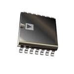
| 描述 | IC DGTL POT 1024POS 100K 14TSSOP数字电位计 IC 1024-pos 1% w/SPI interface |
| DevelopmentKit | EVAL-AD5292EBZ |
| 产品分类 | |
| 品牌 | Analog Devices Inc |
| 产品手册 | |
| 产品图片 |
|
| rohs | 符合RoHS无铅 / 符合限制有害物质指令(RoHS)规范要求 |
| 产品系列 | 数字电位计 IC,Analog Devices AD5292BRUZ-100- |
| 数据手册 | |
| 产品型号 | AD5292BRUZ-100 |
| POT数量 | Single |
| 产品目录页面 | |
| 产品种类 | 数字电位计 IC |
| 供应商器件封装 | 14-TSSOP |
| 其它名称 | AD5292BRUZ100 |
| 包装 | 管件 |
| 商标 | Analog Devices |
| 存储器类型 | 非易失 |
| 安装类型 | 表面贴装 |
| 安装风格 | SMD/SMT |
| 容差 | 1 % |
| 封装 | Tube |
| 封装/外壳 | 14-TSSOP(0.173",4.40mm 宽) |
| 封装/箱体 | TSSOP-14 |
| 工作温度 | -40°C ~ 105°C |
| 工作电源电压 | 5.5 V |
| 工厂包装数量 | 96 |
| 弧刷存储器 | Non Volatile |
| 抽头 | 1024 |
| 接口 | 4 线串行 |
| 数字接口 | SPI |
| 最大工作温度 | + 105 C |
| 最小工作温度 | - 40 C |
| 标准包装 | 96 |
| 每POT分接头 | 1024 |
| 温度系数 | 标准值 35 ppm/°C |
| 特色产品 | http://www.digikey.com/cn/zh/ph/analog-devices/ad5292.html |
| 电压-电源 | 9 V ~ 33 V, ±9 V ~ 16.5 V |
| 电源电压-最大 | 33 V |
| 电源电压-最小 | 9 V |
| 电源电流 | 2 uA |
| 电路数 | 1 |
| 电阻 | 100 kOhms |
| 电阻(Ω) | 100k |
| 系列 | AD5292 |
| 设计资源 | 点击此处下载产品Datasheet点击此处下载产品Datasheet点击此处下载产品Datasheet点击此处下载产品Datasheet点击此处下载产品Datasheet点击此处下载产品Datasheet点击此处下载产品Datasheet |


- 商务部:美国ITC正式对集成电路等产品启动337调查
- 曝三星4nm工艺存在良率问题 高通将骁龙8 Gen1或转产台积电
- 太阳诱电将投资9.5亿元在常州建新厂生产MLCC 预计2023年完工
- 英特尔发布欧洲新工厂建设计划 深化IDM 2.0 战略
- 台积电先进制程称霸业界 有大客户加持明年业绩稳了
- 达到5530亿美元!SIA预计今年全球半导体销售额将创下新高
- 英特尔拟将自动驾驶子公司Mobileye上市 估值或超500亿美元
- 三星加码芯片和SET,合并消费电子和移动部门,撤换高东真等 CEO
- 三星电子宣布重大人事变动 还合并消费电子和移动部门
- 海关总署:前11个月进口集成电路产品价值2.52万亿元 增长14.8%


PDF Datasheet 数据手册内容提取
1024-Position, Digital Potentiometer with Maximum ±1% R-Tolerance Error and 20-TP Memory Enhanced Product AD5292-EP FEATURES FUNCTIONAL BLOCK DIAGRAM Single-channel, 1024-position resolution VDD RESET 20 kΩ nominal resistance POWER-ON AD5292-EP Maximum ±1% nominal resistor tolerance error (resistor RESET performance mode) 20-times programmable wiper memory VLOGIC Rheostat mode temperature coefficient: 35 ppm/°C RDAC Voltage divider temperature coefficient: 5 ppm/°C SCLK REGISTER A SERIAL DATA +9 V to +33 V single-supply operation SYNC INTERFACE W ±9 V to ±16.5 V dual-supply operation OTP SPI-compatible serial interface DIN MEMORY BLOCK B Wiper setting readback SDO Power-on refreshed from 20-TP memory RDY ESuNpHpoArNtsC dEeDfe nPsRe OanDdU aCerTo sFpEaAceT aUpRpElicSa tions (AQEC) VSS EXT_CAP GND 10095-001 Figure 1. Temperature range: −55°C to +125°C Controlled manufacturing baseline 1 assembly/test site 1 fabrication site Product change notification Qualification data available on request APPLICATIONS Mechanical potentiometer replacement Instrumentation: gain and offset adjustment Programmable voltage-to-current conversion Programmable filters, delays, and time constants Programmable power supply Low resolution DAC replacement Sensor calibration GENERAL DESCRIPTION The AD5292-EP is a single-channel, 1024-position digital The AD5292-EP device wiper settings are controllable through potentiometer1 that combines industry leading variable resistor the SPI digital interface. Unlimited adjustments are allowed performance with nonvolatile memory (NVM) in a compact before programming the resistance value into the 20-TP memory. package. This device is capable of operating across a wide voltage The AD5292-EP does not require any external voltage supply range, supporting both dual supply operation at ±10.5 V to ±16.5 to facilitate fuse blow, and there are 20 opportunities for perma- V and single-supply operation at +21 V to +33 V, while ensuring nent programming. During 20-TP activation, a permanent blow less than 1% end-to-end resistor tolerance error and offering 20- fuse command freezes the wiper position (analogous to placing time programmable (20-TP) memory. epoxy on a mechanical trimmer). The guaranteed industry leading low resistor tolerance error The AD5292-EP is available in a compact 14-lead TSSOP feature simplifies open-loop applications as well as precision package. The part is guaranteed to operate over the extended calibration and tolerance matching applications. industrial temperature range of −55°C to +125°C. Additional application and technical information can be found 1 The terms digital potentiometer and RDAC are used interchangeably. in the AD5292 data sheet. Rev. A Document Feedback Information furnished by Analog Devices is believed to be accurate and reliable. However, no responsibility is assumed by Analog Devices for its use, nor for any infringements of patents or other One Technology Way, P.O. Box 9106, Norwood, MA 02062-9106, U.S.A. rights of third parties that may result from its use. Specifications subject to change without notice. No license is granted by implication or otherwise under any patent or patent rights of Analog Devices. Tel: 781.329.4700 ©2011–2018 Analog Devices, Inc. All rights reserved. Trademarks and registered trademarks are the property of their respective owners. Technical Support www.analog.com
AD5292-EP Enhanced Product TABLE OF CONTENTS Features .............................................................................................. 1 Interface Timing Specifications ...................................................5 Enhanced Product Features ............................................................ 1 Absolute Maximum Ratings ............................................................7 Applications ....................................................................................... 1 Thermal Resistance .......................................................................7 Functional Block Diagram .............................................................. 1 ESD Caution...................................................................................7 General Description ......................................................................... 1 Pin Configuration and Function Descriptions ..............................8 Revision History ............................................................................... 2 Typical Performance Characteristics ..............................................9 Specifications ..................................................................................... 3 Test Circuits ..................................................................................... 14 Electrical Characteristics—AD5292-EP .................................... 3 Outline Dimensions ....................................................................... 15 Resistor Performance Mode Code Range ................................. 4 Ordering Guide .......................................................................... 15 REVISION HISTORY 4/2018—Rev. 0 to Rev. A Change to Enhanced Product Features Section ........................... 1 Changes to Ordering Guide .......................................................... 15 9/2011—Revision 0: Initial Version Rev. A | Page 2 of 16
Enhanced Product AD5292-EP SPECIFICATIONS ELECTRICAL CHARACTERISTICS—AD5292-EP V = 21 V to 33 V, V = 0 V; V = 10.5 V to 16.5 V, V = −10.5 V to −16.5 V; V = 2.7 V to 5.5 V, V = V , V = V , DD SS DD SS LOGIC A DD B SS −55°C < T < +125°C, unless otherwise noted. A Table 1. Parameter Symbol Conditions Min Typ1 Max Unit DC CHARACTERISTICS—RHEOSTAT MODE Resolution N 10 Bits Resistor Differential Nonlinearity2 R-DNL RWB, VA = NC −1 +1 LSB Resistor Integral Nonlinearity2 R-INL RAB =20 kΩ, |VDD − VSS| = 26 V to 33 V −2 +2 LSB R-INL RAB =20 kΩ, |VDD − VSS| = 21 V to 26 V −3 +3 LSB Nominal Resistor Tolerance (R-Perf Mode)3 ∆RAB/RAB See Table 2 −1 ±0.5 +1 % Nominal Resistor Tolerance (Normal ∆RAB/RAB ±7 % Mode)4 Resistance Temperature Coefficient (∆RAB/RAB)/∆T × 106 Code = full scale; see Figure 14 35 ppm/°C Wiper Resistance RW Code= zero scale 60 100 Ω DC CHARACTERISTICS—POTENTIOMETER DIVIDER MODE Resolution N 10 Bits Differential Nonlinearity5 DNL −1 +1 LSB Integral Nonlinearity5 INL −2.5 +2.5 LSB Voltage Divider Temperature Coefficient4 (∆VW/VW)/∆T × 106 Code = half scale; see Figure 17 5 ppm/°C Full-Scale Error VWFSE Code = full scale −8 +1 LSB Zero-Scale Error VWZSE Code = zero scale 0 10 LSB RESISTOR TERMINALS Terminal Voltage Range6 VA, VB, VW VSS VDD V Capacitance A, Capacitance B4 CA, CB f = 1 MHz, measured to GND, 85 pF code = half scale Capacitance W4 CW f = 1 MHz, measured to GND, 65 pF code = half scale Common-Mode Leakage Current4 ICM VA = VB = VW −120 ±1 120 nA DIGITAL INPUTS JEDEC compliant Input Logic High4 VIH VLOGIC = 2.7 V to 5.5 V 2.0 V Input Logic Low4 VIL VLOGIC = 2.7 V to 5.5 V 0.8 V Input Current IIL VIN = 0 V or VLOGIC ±1 µA Input Capacitance4 CIL 5 pF DIGITAL OUTPUTS (SDO and RDY) Output High Voltage4 VOH RPULL_UP = 2.2 kΩ to VLOGIC VLOGIC − 0.4 V Output Low Voltage4 VOL RPULL_UP = 2.2 kΩ to VLOGIC GND + 0.4 V Three-State Leakage Current −1 +1 µA Output Capacitance4 COL 5 pF POWER SUPPLIES Single-Supply Power Range VDD VSS = 0 V 9 33 V Dual-Supply Power Range VDD/VSS ±9 ±16.5 V Positive Supply Current IDD VDD/VSS = ±16.5 V 0.1 2 µA Negative Supply Current ISS VDD/VSS = ±16.5 V −2 −0.1 µA Logic Supply Range VLOGIC 2.7 5.5 V Logic Supply Current ILOGIC VLOGIC = 5 V, VIH = 5 V or VIL = GND 1 10 µA OTP Store Current4, 7 ILOGIC_PROG VIH = 5 V or VIL = GND 25 mA OTP Read Current4, 8 ILOGIC_FUSE_READ VIH = 5 V or VIL = GND 25 mA Power Dissipation9 PDISS VIH = 5 V or VIL = GND 8 110 µW Power Supply Rejection Ratio PSRR ∆VDD/∆VSS = ±15 V ± 10% 0.103 %/% Rev. A | Page 3 of 16
AD5292-EP Enhanced Product Parameter Symbol Conditions Min Typ1 Max Unit DYNAMIC CHARACTERISTICS5, 10 Bandwidth BW −3 dB 520 kHz Total Harmonic Distortion THDW VA = 1 V rms, VB = 0 V, f = 1 kHz −93 dB VW Settling Time tS VA = 30 V, VB = 0 V, ±0.5 LSB error band, initial code = zero scale, board capacitance = 170 pF Code = full-scale, normal mode 750 ns Code = full-scale, R-Perf mode 2.5 µs Code = half-scale, normal mode 2.5 µs Code = half-scale, R-Perf mode 5 µs Resistor Noise Density eN_WB Code = half-scale, TA = 25°C, 0 kHz to 10 nV/√Hz 200 kHz 1 Typical values represent average readings at 25°C, VDD = 15 V, VSS = −15 V, and VLOGIC = 5 V. 2 Resistor position nonlinearity error. R-INL is the deviation from an ideal value measured between RWB at Code 0x00B and Code 0x3FF or between RWA at Code 0x3F3 and Code 0x000. R-DNL measures the relative step change from ideal between successive tap positions. The specification is guaranteed in resistor performance mode, with a wiper current of 1 mA for VA < 12 V and 1.2 mA for VA ≥ 12 V. 3 Resistor performance mode. The terms resistor performance mode and R-Perf mode are used interchangeably. 4 Guaranteed by design and characterization, not subject to production test. 5 INL and DNL are measured at VW with the RDAC configured as a potentiometer divider similar to a voltage output DAC. VA = VDD and VB = 0 V. DNL specification limits of ±1 LSB maximum are guaranteed monotonic operating conditions. 6 Resistor Terminal A, Resistor Terminal B, and Resistor Terminal W have no limitations on polarity with respect to each other. Dual-supply operation enables ground- referenced bipolar signal adjustment. 7 Different from operating current; supply current for fuse program lasts approximately 550 µs. 8 Different from operating current; supply current for fuse read lasts approximately 550 µs. 9 PDISS is calculated from (IDD × VDD) + (ISS × VSS) + (ILOGIC × VLOGIC). 10 All dynamic characteristics use VDD = 15 V, VSS = −15 V, and VLOGIC = 5 V. RESISTOR PERFORMANCE MODE CODE RANGE Table 2. −55°C < T < +125°C Resistor A Tolerance per |VDD − VSS| = 30 V to 33 V |VDD − VSS| = 26 V to 30 V |VDD − VSS| = 22 V to 26 V |VDD − VSS| = 21 V to 22 V Code R R R R R R R R WB WA WB WA WB WA WB WA 1% R-Tolerance From 0x1EF From 0x000 From 0x1F4 From 0x000 From 0x1F4 From 0x000 N/A N/A to 0x3FF to 0x210 to 0x3FF to 0x20B to 0x3FF to 0x20B 2% R-Tolerance From 0x0C3 From 0x000 From 0x0E6 From 0x000 From 0x131 From 0x000 From 0x131 From 0x000 to 0x3FF to 0x33C to 0x3FF to 0x319 to 0x3FF to 0x2CE to 0x3FF to 0x2CE 3% R-Tolerance From 0x073 From 0x000 From 0x087 From 0x000 From 0x0AF From 0x000 From 0x0AF From 0x000 to 0x3FF to 0x38C to 0x3FF to 0x378 to 0x3FF to 0x350 to 0x3FF to 0x350 Rev. A | Page 4 of 16
Enhanced Product AD5292-EP INTERFACE TIMING SPECIFICATIONS V /V = ±15 V, V = 2.7 V to 5.5 V, −55°C < T < +125°C. All specifications T to T , unless otherwise noted. DD SS LOGIC A MIN MAX Table 3. Parameter Limit1 Unit Description t2 20 ns min SCLK cycle time 1 t 10 ns min SCLK high time 2 t 10 ns min SCLK low time 3 t 10 ns min SYNC to SCLK falling edge setup time 4 t 5 ns min Data setup time 5 t 5 ns min Data hold time 6 t 1 ns min SCLK falling edge to SYNC rising edge 7 t 4003 ns min Minimum SYNC high time 8 t 14 ns min SYNC rising edge to next SCLK fall ignore 9 t 4 1 ns min RDY rising edge to SYNC falling edge 10 t114 40 ns max SYNC rising edge to RDY fall time t124 2.4 μs max RDY low time, RDAC register write command execute time (R-Perf mode) t124 410 ns max RDY low time, RDAC register write command execute time (normal mode) t124 8 ms max RDY low time, memory program execute time t124 1.5 ms min Software/hardware reset t134 450 ns max RDY low time, RDAC register readback execute time t134 1.3 ms max RDY low time, memory readback execute time t144 450 ns max SCLK rising edge to SDO valid t 20 ns min Minimum RESET pulse width (asynchronous) RESET t 5 2 ms max Power-on OTP restore time POWER-UP 1 All input signals are specified with tR = tF = 1 ns/V (10% to 90% of VDD) and timed from a voltage level of (VIL + VIH)/2. 2 Maximum SCLK frequency is 50 MHz. 3 Refer to t12 and t13 for RDAC register and memory commands operations. 4 RPULL_UP = 2.2 kΩ to VLOGIC, with a capacitance load of 168 pF. 5 Maximum time after VLOGIC is equal to 2.5 V. DB9 (MSB) DB0 (LSB) 0 0 C3 C2 C1 C0 D9 D8 D7 D6 D5 D4 D3 D2 D1 D0 CONTROL BITS DATA BITS 10095-003 Figure 2. Shift Register Content Rev. A | Page 5 of 16
AD5292-EP Enhanced Product Timing Diagrams t4 t2 t1 t7 SCLK t8 t3 t9 SYNC t5 t6 DIN X X C3 C2 D7 D6 D2 D1 D0 SDO t10 t11 t12 RDY RESET tRESET 10095-004 Figure 3. Write Timing Diagram, CPOL = 0, CPHA = 1 SCLK t9 SYNC DIN X X C3 D0 D0 X X C3 D1 D0 t14 SDO X X C3 D1 D0 RDY t11 t13 10095-005 Figure 4. Read Timing Diagram, CPOL = 0, CPHA = 1 Rev. A | Page 6 of 16
Enhanced Product AD5292-EP ABSOLUTE MAXIMUM RATINGS T = 25°C, unless otherwise noted. A Stresses at or above those listed under Absolute Maximum Ratings may cause permanent damage to the product. This is a Table 4. stress rating only; functional operation of the product at these Parameter Rating or any other conditions above those indicated in the operational V to GND −0.3 V to +35 V DD section of this specification is not implied. Operation beyond V to GND +0.3 V to −25 V SS the maximum operating conditions for extended periods may V to GND −0.3 V to +7 V LOGIC affect product reliability. V to V 35 V DD SS V , V , V to GND V − 0.3 V, V + 0.3 V A B W SS DD Digital Input and Output Voltage to GND −0.3 V to VLOGIC + 0.3 V THERMAL RESISTANCE EXT_CAP Voltage to GND −0.3 V to +7 V θ is defined by JEDEC specification JESD-51 and the value is I , I , I JA A B W dependent on the test board and test environment. Continuous ±3 mA Pulsed1 Table 5. Thermal Resistance Frequency > 10 kHz ±3/d2 Package Type θ θ Unit JA JC Frequency ≤ 10 kHz ±3/√d2 14-Lead TSSOP 931 20 °C/W Operating Temperature Range3 −55°C to +125°C Maximum Junction Temperature (T max) 150°C 1 JEDEC 2S2P test board, still air (0 m/sec to 1 m/sec air flow). J Storage Temperature Range −65°C to +150°C Reflow Soldering ESD CAUTION Peak Temperature 260°C Time at Peak Temperature 20 sec to 40 sec Package Power Dissipation (T max − T )/θ J A JA 1 Maximum terminal current is bounded by the maximum current handling of the switches, maximum power dissipation of the package, and maximum applied voltage across any two of the A, B, and W terminals at a given resistance. 2 Pulse duty factor. 3 Includes programming of OTP memory. Rev. A | Page 7 of 16
AD5292-EP Enhanced Product PIN CONFIGURATION AND FUNCTION DESCRIPTIONS RESET 1 14 RDY VSS 2 13 SDO A 3 AD5292-EP 12 SYNC W 4 TOP VIEW 11 SCLK B 5 (Not to Scale) 10 DIN EXT_CVADPD 67 98 GVLNODGIC 10095-006 Figure 5. Pin Configuration Table 6. Pin Function Descriptions Pin No. Mnemonic Description 1 RESET Hardware Reset Pin. Refreshes the RDAC register with the contents of the 20-TP memory register. Factory default loads midscale until the first 20-TP wiper memory location is programmed. RESET is activated at the logic high transition. Tie RESET to V if not used. LOGIC 2 V Negative Supply. Connect to 0 V for single-supply applications. This pin should be decoupled with 0.1 μF SS ceramic capacitors and 10 μF capacitors. 3 A Terminal A of RDAC. V ≤ V ≤ V . SS A DD 4 W Wiper Terminal of RDAC. V ≤ V ≤ V . SS W DD 5 B Terminal B of RDAC. V ≤ V ≤ V . SS B DD 6 V Positive Power Supply. This pin should be decoupled with 0.1 μF ceramic capacitors and 10 μF capacitors. DD 7 EXT_CAP External Capacitor. Connect a 1 μF capacitor to EXT_CAP. This capacitor must have a voltage rating of ≥7 V. 8 V Logic Power Supply; 2.7 V to 5.5 V. This pin should be decoupled with 0.1 μF ceramic capacitors and 10 μF LOGIC capacitors. 9 GND Ground Pin, Logic Ground Reference. 10 DIN Serial Data Input. The AD5292-EP has a 16-bit shift register. Data is clocked into the register on the falling edge of the serial clock input. 11 SCLK Serial Clock Input. Data is clocked into the shift register on the falling edge of the serial clock input. Data can be transferred at rates up to 50 MHz. 12 SYNC Falling Edge Synchronization Signal. This is the frame synchronization signal for the input data. When SYNC goes low, it enables the shift register and data is transferred in on the falling edges of the following clocks. The selected register is updated on the rising edge of SYNC following the 16th clock cycle. If SYNC is taken high before the 16th clock cycle, the rising edge of SYNC acts as an interrupt, and the write sequence is ignored by the DAC. 13 SDO Serial Data Output. This open-drain output requires an external pull-up resistor. SDO can be used to clock data from the shift register in daisy-chain mode or in readback mode. 14 RDY Ready Pin. This active-high open-drain output identifies the completion of a write or read operation to or from the RDAC register or memory. Rev. A | Page 8 of 16
Enhanced Product AD5292-EP TYPICAL PERFORMANCE CHARACTERISTICS 1.0 0.6 –40°C 0.8 +25°C 0.5 +105°C 0.6 0.4 0.4 0.3 NL (LSB) 0.20 NL (LSB) 00..12 I –0.2 D 0 –0.4 –0.1 –0.6 –0.8 –0.2 –40°C +25°C +105°C –1.00 128 256 38C4ODE 5(D12ecima6l4)0 768 896 1023 10095-106 –0.30 128 256 38C4ODE 5(D12ecima6l4)0 768 896 1023 10095-007 Figure 6. R-INL in R-Perf Mode vs. Code Figure 9. R-DNL in R-Perf Mode vs. Code 1.5 0.6 0.5 1.0 0.4 0.5 0.3 B) B) S S NL (L 0 NL (L 0.2 I D 0.1 –0.5 0 –1.0 –0.1 –40°C +25°C +105°C –40°C +25°C +105°C –1.50 128 256 38C4ODE 5(D12ecima6l4)0 768 896 1023 10095-014 –0.20 128 256 38C4ODE 5(D12ecima6l4)0 768 896 1023 10095-015 Figure 7. INL in R-Perf Mode vs. Code Figure 10. DNL in R-Perf Mode vs. Code 1.0 0.15 0.8 0.10 0.6 0.05 0.4 B) B) 0 INL (LS 0.2 DNL (LS–0.05 0 –0.10 –0.2 –0.4 –0.15 –40°C +25°C +105°C –40°C +25°C +105°C –0.60 128 256 38C4ODE 5(D12ecima6l4)0 768 896 1023 10095-010 –0.200 128 256 38C4ODE 5(D12ecima6l4)0 768 896 1023 10095-011 Figure 8. R-INL in Normal Mode vs. Code Figure 11. R-DNL in Normal Mode vs. Code Rev. A | Page 9 of 16
AD5292-EP Enhanced Product 0.8 0.10 –40°C –40°C +25°C +25°C 0.6 +105°C 0.05 +105°C 0.4 0 0.2 B) B) NL (LS 0 NL (LS–0.05 I D –0.2 –0.10 –0.4 –0.15 –0.6 –0.80 128 256 38C4ODE 5(D12ecima6l4)0 768 896 1023 10095-018 –0.200 128 256 38C4ODE 5(D12ecima6l4)0 768 896 1023 10095-019 Figure 12. INL in Normal Mode vs. Code Figure 15. DNL in Normal Mode vs. Code 450 0.20 400 VVDLODG/VICS S= =+ 5±V15V 0.18 VDD = ±15V 350 A) 0.16 ILOGIC m T (nA) 300 (OGIC 0.14 N 250 L 0.12 SUPPLY CURRE 211050000 IDD UPPLY CURRENT I 000...001680 50 S 0.04 0 0.02 ISS –50–40–30–20–10 0 1T0EM2P0ER3A0TU4R0E (5°0C)60 70 80 90 100 10095-022 00 0.5 1.0 D1I.G5ITA2L. 0INPU2T.5 VOL3T.A0GE 3(V.5) 4.0 4.5 5.0 10095-031 Figure 13. Supply Current (IDD, ISS, ILOGIC) vs. Temperature Figure 16. Supply Current ILOGIC vs. Digital Input Voltage 700 700 C) 600 VVDSSD == 03V0V m/°C) 600 VVDSSD == 03V0V pm/° O (pp ODE TEMPCO (p 543000000 R MODE TEMPC 543000000 M E STAT 200 OMET 200 O TI E N H E R 100 T 100 O P 00 256 CODE 5(D12ecimal) 768 1023 10095-024 00 256 CODE 5(D12ecimal) 768 1023 10095-023 Figure 14. Rheostat Mode Tempco ΔRWB/ΔT vs. Code Figure 17. Potentiometer Mode Tempco ΔRWB/ΔT vs. Code Rev. A | Page 10 of 16
Enhanced Product AD5292-EP 0 0 –5 0x200 –10 –10 0x100 –15 –20 0x080 N (dB) ––2250 0x040 R (dB)–30 AI 0x020 R G –30 PS–40 0x010 –35 0x008 –50 –40 –45 0x004 –60 0x002 0x001 –5010 100 FR1kEQUENCY 1(H0kz) 100k 1M 10095-025 –70100 1k FREQU1E0NkCY (Hz) 100k 1M 10095-026 Figure 18. 20 kΩ Gain vs. Frequency vs. Code Figure 21. Power Supply Rejection Ratio vs. Frequency 0 0 VDD/VSS = ±15V VDD/VSS = ±15V, CODE = HALF SCALE CODE = HALF SCALE –15 VIN = 1V rms –20 fIN = 1kHz NOISE BW = 22kHz NOISE BW = 22kHz –30 –40 B) –45 B) N (d N (d –60 HD + –60 HD + –80 T –75 T –100 –90 –120 –105 –120100 1k FREQUENC1Y0 (kHz) 100k 10095-027 –1400.001 0.01 AMPLITU0D.1E (V rms) 1 10 10095-220 Figure 19. THD + Noise vs. Frequency Figure 22. THD + Noise vs. Amplitude 1,000,000 35 900,000 0pF 75pF 30 150pF 800,000 250pF A) 25 m H (Hz)670000,,000000 T I (DD 20 T N WID500,000 RRE 15 D U N400,000 C BA LY 10 300,000 PP SU 5 200,000 100,000 0 00 8 16 CO3D2E (Deci6m4al) 128 256 512 10095-222 –5–0.4 –0.2 0 0.2 TIM0E. 4(ms) 0.6 0.8 1.0 1.2 10095-034 Figure 20. Bandwidth vs. Code vs. Net Capacitance Figure 23. IDD Waveform While Blowing/Reading Fuse Rev. A | Page 11 of 16
AD5292-EP Enhanced Product 35 40 VWB, CODE: FULL SCALE, VDD/VSS = 30V/0V VDD/VSS = ±15V 30 NORMAL MODE VVLAO =G VICD =D 5V 32 VVAB== VVDSSD VB = VSS 24 CODE = HALF CODE 25 16 VOLTAGE (V) 112050 V W B , C O D E : FRU-PLLE RSFC AMLOED,E VOLTAGE (μV) –808 SYNC –16 5 VWB, CODE: HALF-SCALE, –24 NORMAL MODE 0 VWB, CODE: HALF-SCALE, –32 R-PERF MODE –5–2 –1 0 1 2 3 4 5T6IME7 (µs8) 9 10 11 12 13 14 15 10095-033 –40–0.5 0 5 10 15TIM2E0 (µs)25 30 35 40 45 10095-032 Figure 24. Large-Signal Settling Time from Code Zero Scale Figure 27. Digital Feedthrough 8 6 VDD/VSS = 30V/0V VDD/VSS = ±15V 7 VVAB == VVDSSD 5 VLOGIC = +5V mA) 6 (X 4 A WB_M5 E (V) 3 ETICAL I 34 VOLTAG 2 R O E 1 H 2 T 1 0 00 256 CODE 5(D12ecimal) 768 1023 10095-029 –1–1.0 –0.4 0.2 0.8 1.4 2.0 2.6 3.2TIM3.8E (m4.4s)5.0 5.6 6.2 6.8 7.4 8.0 8.6 10095-036 Figure 25. Theoretical Maximum Current vs. Code Figure 28. VEXT_CAP Waveform While Reading Fuse Or Calibration 1.2 8 VDD/VSS = ±15V VDD/VSS = ±15V 1.0 VLOGIC = +5V VLOGIC = +5V VA = VDD 0.8 VB = VSS 6 0.6 V) 0.4 V) 3 E ( E ( AG 0.2 AG T T L L VO 0 VO 2 –0.2 –0.4 0 –0.6 –0.8–2 0 2 4 6TIME (8µs) 10 12 14 16 10095-035 –2–2.0 –0.8 0.4 1.6 2.8 4.0 5.2 6.4TIM7.6E (8.8ms)10.0 11.2 12.4 13.6 14.8 16.0 17.2 10095-037 Figure 26. Maximum Transition Glitch Figure 29. VEXT_CAP Waveform While Writing Fuse Rev. A | Page 12 of 16
Enhanced Product AD5292-EP 300 80 VDD/VSS= ±15V VA = VDD VB = VSS 70 TEMPERATURE = 25°C 250 60 S S E200 E OD OD 50 C C F F O150 O 40 R R E E B B M M 30 NU100 NU 20 50 10 0–40–30–20–10 0 1T0EM2P0ER3A0TU4R0E (5°0C)60 70 80 90 100 10095-056 021 26VOLTAGE VDD/VSS30 33 10095-219 Figure 30. Code Range > 1% R-Tolerance Error vs. Temperature Figure 31. Code Range > 1% R-Tolerance Error vs. Voltage Rev. A | Page 13 of 16
AD5292-EP Enhanced Product TEST CIRCUITS Figure 32 to Figure 37 define the test conditions used in the Specifications section. NC DUT A IW VA W V+ = VDD ± 10% B NC = NO CVOMNSNECT 10095-041 V+ ~ VDD BA W VMS PPSSSR R(% (d/%B)) == ΔΔ20VV MDloDSg%%ΔΔVVMDDS 10095-044 Figure 32. Resistor Position Nonlinearity Error Figure 35. Power Supply Sensitivity (PSS, PSRR) (Rheostat Operation; R-INL, R-DNL) A +15V DUT V+ = VDD W A 1LSB = V+/2N VIN DUT V+ W OFFSET B OP42 VOUT B GND VMS 10095-042 2.5V –15V 10095-047 Figure 33. Potentiometer Divider Nonlinearity Error Figure 36. Gain vs. Frequency (INL, DNL) +15V –15V NC GND 0.1V GND DAUTW CODE = 0x00+RRWWB == RIWW2BB DVVDUSDSTGND BA W ICM +–1155VV B IWB –0.1V GND A = NC VSSTO VDD 10095-043 NC+15V –15VGND NC = NO CONNECT 10095-048 Figure 34. Wiper Resistance Figure 37. Common-Mode Leakage Current Rev. A | Page 14 of 16
Enhanced Product AD5292-EP OUTLINE DIMENSIONS 5.10 5.00 4.90 14 8 4.50 4.40 6.40 BSC 4.30 1 7 PIN 1 0.65 BSC 1.05 1.00 1M.A20X 0.20 0.80 0.09 0.75 0.15 8° 0.60 0.05 0.30 SPLEAATNIENG 0° 0.45 COPLANARITY 0.19 0.10 COMPLIANT TO JEDEC STANDARDS MO-153-AB-1 061908-A Figure 38. 14-Lead Thin Shrink Small Outline Package [TSSOP] (RU-14) Dimensions shown in millimeters ORDERING GUIDE Model1 R (kΩ) Resolution Memory Temperature Range Package Description Package Option AB AD5292SRU-20-EP 20 1024 20-TP −55°C to +125°C 14-Lead TSSOP RU-14 AD5292SRUZ-20-EP 20 1024 20-TP −55°C to +125°C 14-Lead TSSOP RU-14 1 Z = RoHS Compliant Part. Rev. A | Page 15 of 16
AD5292-EP Enhanced Product NOTES ©2011–2018 Analog Devices, Inc. All rights reserved. Trademarks and registered trademarks are the property of their respective owners. D10095-0-4/18(A) Rev. A | Page 16 of 16
Mouser Electronics Authorized Distributor Click to View Pricing, Inventory, Delivery & Lifecycle Information: A nalog Devices Inc.: AD5291BRUZ-20 AD5292BRUZ-20 AD5292BRUZ-50 AD5292BRUZ-100-RL7 AD5292BRUZ-100 EVAL- AD5292EBZ AD5292BRUZ-50-RL7 AD5292SRU-20-EP AD5292BRUZ-20-RL7 AD5292SRUZ-20-EP