ICGOO在线商城 > 集成电路(IC) > 数据采集 - 数字电位器 > AD5204BRUZ100
 Datasheet下载
- 型号: AD5204BRUZ100
- 制造商: Analog
- 库位|库存: xxxx|xxxx
- 要求:
| 数量阶梯 | 香港交货 | 国内含税 |
| +xxxx | $xxxx | ¥xxxx |
查看当月历史价格
查看今年历史价格
AD5204BRUZ100产品简介:
ICGOO电子元器件商城为您提供AD5204BRUZ100由Analog设计生产,在icgoo商城现货销售,并且可以通过原厂、代理商等渠道进行代购。 AD5204BRUZ100价格参考。AnalogAD5204BRUZ100封装/规格:数据采集 - 数字电位器, Digital Potentiometer 100k Ohm 4 Circuit 256 Taps SPI Interface 24-TSSOP。您可以下载AD5204BRUZ100参考资料、Datasheet数据手册功能说明书,资料中有AD5204BRUZ100 详细功能的应用电路图电压和使用方法及教程。
AD5204BRUZ100 是由 Analog Devices Inc. 生产的一款数字电位器,属于数据采集类产品。该器件具有四个独立的通道,每个通道可以实现电阻值的数字化调节,广泛应用于需要精确电阻控制的各种电子系统中。

 应用场景:

1. 音频设备:
   - 在音频设备中,如耳机放大器、音响系统等,AD5204BRUZ100 可用于音量控制、平衡调节等。通过数字接口调整电位器的阻值,用户可以更精确地控制音频信号的增益或衰减,确保音质的一致性和稳定性。

2. 工业自动化:
   - 在工业控制系统中,AD5204BRUZ100 可以用于传感器信号调理电路中的增益调节。例如,在温度、压力等传感器的应用中,通过数字电位器动态调整放大器的增益,确保信号在不同环境条件下的线性度和精度。

3. 医疗设备:
   - 医疗设备如心电图机、监护仪等对信号的精确处理要求极高。AD5204BRUZ100 可用于这些设备中的前端信号调理电路,帮助实现信号的精确放大和滤波,确保测量结果的准确性。

4. 通信设备:
   - 在通信系统中,AD5204BRUZ100 可用于射频(RF)前端的匹配网络调节。通过数字控制电位器的阻值,可以优化天线与发射/接收电路之间的匹配,提高信号传输效率和抗干扰能力。

5. 消费电子产品:
   - 消费电子产品如智能手表、智能家居控制器等也广泛应用数字电位器。AD5204BRUZ100 可用于调节显示屏亮度、背光控制等功能,提供更加智能化的用户体验。

6. 测试与测量仪器:
   - 测试与测量仪器如示波器、万用表等需要高精度的电阻调节功能。AD5204BRUZ100 可用于这些仪器中的校准电路,确保测量结果的准确性和重复性。

总之,AD5204BRUZ100 以其多通道、高精度、低功耗等特点,适用于各种需要精确电阻控制的应用场景,能够显著提升系统的性能和可靠性。
| 参数 | 数值 |
| 产品目录 | 集成电路 (IC)半导体 |
| 描述 | IC DGTL POT 256POS 100K 24TSSOP数字电位计 IC IC 4-CH |
| DevelopmentKit | EVAL-AD5204SDZ |
| 产品分类 | |
| 品牌 | Analog Devices |
| 产品手册 | |
| 产品图片 |
|
| rohs | 符合RoHS无铅 / 符合限制有害物质指令(RoHS)规范要求 |
| 产品系列 | 数字电位计 IC,Analog Devices AD5204BRUZ100- |
| 数据手册 | |
| 产品型号 | AD5204BRUZ100 |
| PCN过时产品 | |
| POT数量 | Quad |
| 产品种类 | 数字电位计 IC |
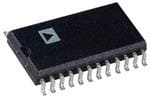
| 供应商器件封装 | 24-TSSOP |
| 包装 | 管件 |
| 商标 | Analog Devices |
| 存储器类型 | 易失 |
| 安装类型 | 表面贴装 |
| 安装风格 | SMD/SMT |
| 容差 | 30 % |
| 封装 | Tube |
| 封装/外壳 | 24-TSSOP(0.173",4.40mm 宽) |
| 封装/箱体 | TSSOP-24 |
| 工作温度 | -40°C ~ 85°C |
| 工作电源电压 | 2.7 V |
| 工厂包装数量 | 62 |
| 弧刷存储器 | Volatile |
| 抽头 | 256 |
| 接口 | 4 线 SPI(芯片选择) |
| 数字接口 | SPI |
| 最大工作温度 | + 85 C |
| 标准包装 | 62 |
| 每POT分接头 | 256 |
| 温度系数 | 700 PPM / C |
| 电压-电源 | 2.7 V ~ 5.5 V, ±2.3 V ~ 2.7 V |
| 电源电流 | 12 uA |
| 电路数 | 4 |
| 电阻 | 100 kOhms |
| 电阻(Ω) | 100k |
| 系列 | AD5204 |
| 缓冲刷 | Buffered |


- 商务部:美国ITC正式对集成电路等产品启动337调查
- 曝三星4nm工艺存在良率问题 高通将骁龙8 Gen1或转产台积电
- 太阳诱电将投资9.5亿元在常州建新厂生产MLCC 预计2023年完工
- 英特尔发布欧洲新工厂建设计划 深化IDM 2.0 战略
- 台积电先进制程称霸业界 有大客户加持明年业绩稳了
- 达到5530亿美元!SIA预计今年全球半导体销售额将创下新高
- 英特尔拟将自动驾驶子公司Mobileye上市 估值或超500亿美元
- 三星加码芯片和SET,合并消费电子和移动部门,撤换高东真等 CEO
- 三星电子宣布重大人事变动 还合并消费电子和移动部门
- 海关总署:前11个月进口集成电路产品价值2.52万亿元 增长14.8%


PDF Datasheet 数据手册内容提取
4-/6-Channel Digital Potentiometers Data Sheet AD5204/AD5206 FEATURES FUNCTIONAL BLOCK DIAGRAMS 256 positions CS AD5204 VDD Multiple independently programmable channels AD5204—4-channel CLK D7 A1 EN W1 AD5206—6-channel RDAC Potentiometer replacement AA21 ADDEDCR LAT1CH B1 Terminal resistance of 10 kΩ, 50 kΩ, 100 kΩ SDO DO A0 D0 R D7 3-wire SPI-compatible serial data input +2.7 V to +5.5 V single-supply operation; ±2.7 V dual-supply SER operation REG D7 A4 Power-on midscale preset W4 APPLICATIONS SDI DI D0 LRADTACCH B4 4 8 SHDN Mechanical potentiometer replacement D0 POWER-ON R VSS IPPnrrsootggrurraammmemmntaaabbtllieeo nvfi:ol tgletaarisgn, e,d o-etfolfas-yceust, ra trdiemjnuets ctcmoonnevsnettar snitosn GND PRESET PR 06884-001 Figure 1. Line impedance matching GENERAL DESCRIPTION CS AD5206 VDD The AD5204/AD5206 provide 4-/6-channel, 256-position CLK D7 A1 EN W1 digitally controlled variable resistor (VR) devices. These RDAC devices perform the same electronic adjustment function as a AA21 ADDEDCR LAT1CH B1 potentiometer or variable resistor. Each channel of the AD5204/ A0 D0 R D7 AD5206 contains a fixed resistor with a wiper contact that taps the fixed resistor value at a point determined by a digital code SER REG loaded into the SPI-compatible serial-input register. The D7 A6 resistance between the wiper and either endpoint of the fixed W6 resistor varies linearly with respect to the digital code transferred SDI DI D0 LRADTACCH B6 6 into the VR latch. The variable resistor offers a completely 8 D0 R programmable value of resistance between the A terminal and ttehrem wiinpaelr r oesri sthtaen Bce t eorfm 10in kaΩl a, n5d0 tkhΩe ,w oirp 1er0.0 T khΩe fhixaes da An-otmo-iBn al GND POPWREESRE-OTN VSS 06884-002 Figure 2. temperature coefficient of 700 ppm/°C. An optional reset (PR) pin forces all the AD5204 wipers to the Each VR has its own VR latch that holds its programmed midscale position by loading 0x80 into the VR latch. resistance value. These VR latches are updated from an internal serial-to-parallel shift register that is loaded from a standard The AD5204/AD5206 are available in the 24-lead surface- 3-wire serial-input digital interface. Eleven data bits make up mount SOIC, TSSOP, and PDIP packages. The AD5204 is also the data-word clocked into the serial input register. The first available in a 32-lead, 5 mm × 5 mm LFCSP package. All parts are three bits are decoded to determine which VR latch is loaded guaranteed to operate over the extended industrial temperature with the last eight bits of the data-word when the CS strobe is range of −40°C to +85°C. For additional single-, dual-, and quad- channel devices, see the AD8400/AD8402/AD8403 data sheets. returned to logic high. A serial data output pin at the opposite end of the serial register (AD5204 only) allows simple daisy chaining in multiple VR applications without requiring additional external decoding logic. Rev. D Document Feedback Information furnished by Analog Devices is believed to be accurate and reliable. However, no responsibility is assumed by Analog Devices for its use, nor for any infringements of patents or other One Technology Way, P.O. Box 9106, Norwood, MA 02062-9106, U.S.A. rights of third parties that may result from its use. Specifications subject to change without notice. No license is granted by implication or otherwise under any patent or patent rights of Analog Devices. Tel: 781.329.4700 ©1999–2015 Analog Devices, Inc. All rights reserved. Trademarks and registered trademarks are the property of their respective owners. Technical Support www.analog.com
AD5204/AD5206 Data Sheet TABLE OF CONTENTS Features .............................................................................................. 1 Typical Performance Characteristics ........................................... 10 Applications ....................................................................................... 1 Operation ......................................................................................... 12 General Description ......................................................................... 1 Programming the Variable Resistor ............................................. 13 Functional Block Diagrams ............................................................. 1 Rheostat Operation .................................................................... 13 Revision History ............................................................................... 2 Programming the Potentiometer Divider ................................... 14 Specifications ..................................................................................... 3 Voltage Output Operation......................................................... 14 Electrical Characteristics ............................................................. 3 Digital Interfacing .......................................................................... 15 Timing Diagrams .............................................................................. 5 Test Circuits ..................................................................................... 16 Absolute Maximum Ratings ............................................................ 6 Outline Dimensions ....................................................................... 17 ESD Caution .................................................................................. 6 Ordering Guide .......................................................................... 18 Pin Configurations and Function Descriptions ........................... 7 REVISION HISTORY 6/15—Rev. C to Rev. D 11/07—Rev. 0 to Rev. A Updated Outline Dimensions ....................................................... 18 Updated Format .................................................................. Universal Changes to Ordering Guide .......................................................... 19 Added 32-Lead LFCSP Package ....................................... Universal Changed R to R ............................................................ Universal BA AB 7/10—Rev. B to Rev. C Changes to Absolute Maximum Ratings ........................................ 6 Changes to Digital Input and Output Voltage to GND Changes to Operation Section ...................................................... 12 Parameter, Table 2 ............................................................................. 6 Updated Outline Dimensions ....................................................... 17 Changes to Ordering Guide .......................................................... 18 Changes to Ordering Guide .......................................................... 18 5/09—Rev. A to Rev. B 9/99—Revision 0: Initial Version Changes to Table 1 ............................................................................ 3 Changes to Absolute Maximum Ratings ....................................... 6 Changes to Figure 7 .......................................................................... 8 Changes to Table 4 ............................................................................ 8 Rev. D | Page 2 of 20
Data Sheet AD5204/AD5206 SPECIFICATIONS ELECTRICAL CHARACTERISTICS V = 5 V ± 10% or 3 V ± 10%, V = 0 V, V = V , V = 0 V, −40°C < T < +85°C, unless otherwise noted. DD SS A DD B A Table 1. Parameter Symbol Test Conditions/Comments Min Typ1 Max Unit DC CHARACTERISTICS RHEOSTAT MODE2 Resistor Differential NL3 R-DNL R , V = no connect −1 ±0.25 +1 LSB WB A Resistor Nonlinearity Error3 R-INL R , V = no connect −2 ±0.5 +2 LSB WB A Nominal Resistor Tolerance4 ΔR T = 25°C −30 +30 % AB A Resistance Temperature Coefficient ΔR /ΔT V = V , wiper = no connect 700 ppm/°C AB AB DD Nominal Resistance Match ΔR/R Channel 1 to Channel 2, Channel 3, and 0.25 1.5 % AB Channel 4, or to Channel 5 and Channel 6; V = V AB DD Wiper Resistance R I = 1 V/R, V = 5 V 50 100 Ω W W DD DC CHARACTERISTICS POTENTIOMETER DIVIDER MODE2 Resolution N 8 Bits Differential Nonlinearity5 DNL −1 ±0.25 +1 LSB Integral Nonlinearity5 INL −2 ±0.5 +2 LSB Voltage Divider Temperature Coefficient ΔV /ΔT Code = 0x40 15 ppm/°C W Full-Scale Error V Code = 0x7F −2 −1 0 LSB WFSE Zero-Scale Error V Code = 0x00 0 1 2 LSB WZSE RESISTOR TERMINALS Voltage Range6 V , V , V V V V A B W SS DD Capacitance7 Ax, Bx C , C f = 1 MHz, measured to GND, code = 0x40 45 pF A B Capacitance7 Wx C f = 1 MHz, measured to GND, code = 0x40 60 pF W Shutdown Current8 I 0.01 5 μA A_SD Common-Mode Leakage I V = V = V = 0, V = +2.7 V, V = −2.5 V 1 nA CM A B W DD SS DIGITAL INPUTS AND OUTPUTS Input Logic High V V = 5 V/3 V 2.4/2.1 V IH DD Input Logic Low V V = 5 V/3 V 0.8/0.6 V IL DD Output Logic High V R = 1 kΩ to 5 V 4.9 V OH PULL–UP Output Logic Low V I = 1.6 mA, V = 5 V 0.4 V OL OL LOGIC Input Current I V = 0 V or 5 V ±1 μA IL IN Input Capacitance7 C 5 pF IL POWER SUPPLIES Power Single-Supply Range V range V = 0 V 2.7 5.5 V DD SS Power Dual-Supply Range V /V range ±2.3 ±2.7 V DD SS Positive Supply Current I V = 5 V or V = 0 V 12 60 μA DD IH IL Negative Supply Current I V = −2.5 V, V = +2.7 V 12 60 μA SS SS DD Power Dissipation9 P V = 5 V or V = 0 V 0.3 mW DISS IH IL Power Supply Sensitivity PSS ΔV = 5 V ± 10% 0.0002 0.005 %/% DD DYNAMIC CHARACTERISTICS7, 10 Bandwidth −3 dB BW_10K R = 10 kΩ 721 kHz AB BW_50K R = 50 kΩ 137 kHz AB BW_100K R = 100 kΩ 69 kHz AB Total Harmonic Distortion THD V = 1.414 V rms, V = 0 V dc, f = 1 kHz 0.004 % W A B VW Settling Time (10 kΩ/50 kΩ/100 kΩ) t V = 5 V, V = 0 V, ±1 LSB error band 2/9/18 μs S A B Resistor Noise Voltage e R = 5 kΩ, f = 1 kHz, PR = 0 9 nV/√Hz N_WB WB Rev. D | Page 3 of 20
AD5204/AD5206 Data Sheet Parameter Symbol Test Conditions/Comments Min Typ1 Max Unit INTERFACE TIMING CHARACTERISTICS7, 11, 12 Input Clock Pulse Width t , t Clock level high or low 20 ns CH CL Data Setup Time t 5 ns DS Data Hold Time t 5 ns DH CLK-to-SDO Propagation Delay13 t R = 2 kΩ , C < 20 pF 1 150 ns PD L L CS Setup Time t 15 ns CSS CS High Pulse Width t 40 ns CSW Reset Pulse Width t 90 ns RS CLK Fall to CS Fall Setup t 0 ns CSH0 CLK Fall to CS Rise Hold Time t 0 ns CSH1 CS Rise to Clock Rise Setup t 10 ns CS1 1 Typicals represent average readings at 25°C and VDD = 5 V. 2 Applies to all VRs. 3 Resistor position nonlinearity error (R-INL) is the deviation from an ideal value measured between the maximum resistance and the minimum resistance wiper positions. R-DNL measures the relative step change from the ideal position between successive tap positions. Parts are guaranteed monotonic. See the test circuit in Figure 28. IW = VDD/R for both VDD = 3 V and VDD = 5 V. 4 VAB = VDD, wiper (VW) = no connect. 5 INL and DNL are measured at VW with the RDAC configured as a potentiometer divider similar to a voltage output DAC. VA = VDD and VB = 0 V. DNL specification limits of ±1 LSB maximum are guaranteed monotonic at operating conditions. See the test circuit in Figure 27. 6 Resistor Terminal A, Terminal B, and Wiper W have no limitations on polarity with respect to each other. 7 Guaranteed by design and not subject to production test. 8 Measured at the Ax terminals. All Ax terminals are open circuited in shutdown mode. 9 PDISS is calculated from (IDD × VDD). CMOS logic level inputs result in minimum power dissipation. 10 All dynamic characteristics use VDD = 5 V. 11 Applies to all parts. 12 See the timing diagrams (Figure 3 to Figure 5) for the location of the measured values. All input control voltages are specified with tR = tF = 2.5 ns (10% to 90% of 3 V) and timed from a voltage level of 1.5 V. Switching characteristics are measured using both VDD = 3 V and VDD = 5 V. 13 The propagation delay depends on the values of VDD, RL, and CL (see the Operation section). Rev. D | Page 4 of 20
Data Sheet AD5204/AD5206 TIMING DIAGRAMS 1 SDI A2 A1 A0 D7 D6 D5 D4 D3 D2 D1 D0 0 CLK 1 0 1 RDAC LATCH LOAD CS 0 VOUTVD0VD 06884-003 Figure 3. Timing Diagram SDI 1 Ax OR Dx Ax OR Dx (DATA IN) 0 tDS tDH SDO 1 Ax OR Dx Ax OR Dx (DATA OUT) 0 t PD_MAX t 1 CH tCS1 CLK 0 tCSH0 tCL tCSH1 t 1 CSS CS tCSW 0 t S VOUT V0VDD ±1 LSB ERROR BAND ±1 LSB 06884-004 Figure 4. Detailed Timing Diagram t 1 RS PR 0 t S VOUT V0DVD ±1 LSB ERROR BAND ±1 LSB 06884-005 Figure 5. AD5204 Preset Timing Diagram Rev. D | Page 5 of 20
AD5204/AD5206 Data Sheet ABSOLUTE MAXIMUM RATINGS T = 25°C, unless otherwise noted. Stresses at or above those listed under Absolute Maximum A Ratings may cause permanent damage to the product. This is a Table 2. stress rating only; functional operation of the product at these Parameter Rating or any other conditions above those indicated in the operational VDD to GND −0.3 V to +7 V section of this specification is not implied. Operation beyond VSS to GND 0 V to −7 V the maximum operating conditions for extended periods may VDD to VSS 7 V affect product reliability. V , V , V to GND V , V A B W SS DD I , I , I A B W Pulsed1 ±20 mA ESD CAUTION Continuous 10 kΩ End-to-End Resistance ±11 mA 50 kΩ and 100 kΩ End-to-End ±2.5 mA Resistance Digital Input and Output Voltage −0.3 V to (V + 0.3 V) or 7 V DD to GND (whichever is less) Operating Temperature Range −40°C to +85°C Maximum Junction Temperature 150°C (T max) J Storage Temperature −65°C to +150°C Reflow Soldering Peak Temperature 260°C Time at Peak Temperature 20 sec to 40 sec Package Power Dissipation (T max − T )/θ J A JA Thermal Resistance, θ 2 JA PDIP (N-24-1) 63°C/W SOIC (RW-24) 52°C/W TSSOP (RU-24) 50°C/W LFCSP (CP-32-3) 32.5°C/W 1 Maximum terminal current is bounded by the maximum current handling of the switches, maximum power dissipation of the package, and maximum applied voltage across any two of the A, B, and W terminals at a given resistance. 2 Thermal resistance (JEDEC 4-layer (2S2P) board). Paddle soldered to board. Rev. D | Page 6 of 20
Data Sheet AD5204/AD5206 PIN CONFIGURATIONS AND FUNCTION DESCRIPTIONS NC 1 24 B4 NC 2 23 W4 GND 3 22 A4 CS 4 21 B2 AD5204 PR 5 20 W2 TOP VIEW VDD 6 (Not to Scale) 19 A2 SHDN 7 18 A1 SDI 8 17 W1 CLK 9 16 B1 SDO 10 15 A3 VSS 11 14 W3 NC 12NC = NO CONNECT13 B3 06884-006 Figure 6. AD5204 SOIC/TSSOP Pin Configuration Table 3. AD5204 SOIC/TSSOP Pin Function Descriptions Pin No. Name Description 1, 2, 12 NC Not Connected. 3 GND Ground. 4 CS Chip Select Input (Active Low). When CS returns high, data in the serial input register is decoded based on the address bits, and then it is loaded into the target RDAC latch. 5 PR Preset to Midscale (Active Low). This pin sets the RDAC registers to 0x80. 6 V Positive Power Supply. This pin is specified for operation at both 3 V and 5 V. It is the sum of |V | + |V | < 5.5 V. DD DD SS 7 SHDN Terminal A Open-Circuit Shutdown (Active Low Input). This pin controls VR 1 through VR 4. 8 SDI Serial Data Input. Data is input MSB first. 9 CLK Serial Clock Input. This pin is positive edge triggered. 10 SDO Serial Data Output. This pin is an open-drain transistor and requires a pull-up resistor. 11 V Negative Power Supply. This pin is specified for operation at both 0 V and −2.7 V. It is the sum of |V | + |V | < 5.5 V. SS DD SS 13 B3 Terminal B RDAC 3. 14 W3 Wiper RDAC 3. Address = 010. 2 15 A3 Terminal A RDAC 3. 16 B1 Terminal B RDAC 1. 17 W1 Wiper RDAC 1. Address = 000. 2 18 A1 Terminal A RDAC 1. 19 A2 Terminal A RDAC 2. 20 W2 Wiper RDAC 2. Address = 001. 2 21 B2 Terminal B RDAC 2. 22 A4 Terminal A RDAC 4. 23 W4 Wiper RDAC 4. Address = 011. 2 24 B4 Terminal B RDAC 4. Rev. D | Page 7 of 20
AD5204/AD5206 Data Sheet N SDO CLK SDI SHD VDD PR CS GND 32 31 30 29 28 27 26 25 VSS 1 24 NC PIN 1 NC 2 INDICATOR 23 NC NC 3 22 NC AD5204 NC 4 21 NC NC 5 (NToOtPtoVSIEcaWle) 20 B4 B3 6 19 W4 W3 7 18 A4 A3 8 17 NC 9 10 11 12 13 14 15 16 C 1 1 1 2 2 2 C N B W A A W B N NOTES 1. NC = NO CONNECT. 2. THE LFCSP PACKAGE HAS AN EXPOSED PGGANRDDOD UALNNEDD T PTHLHAAETT AESS.HSOOUCLIDA TBEED C POCNBNECTED TO 06884-053 Figure 7. AD5204 LFCSP Pin Configuration Table 4. AD5204 LFCSP Pin Function Descriptions Pin No. Name Description 1 V Negative Power Supply. This pin is specified for operation at both 0 V and −2.7 V. It is the sum of |V | + |V | < 5.5 V. SS DD SS 2 to 5, 9, NC Not Connected. 16, 17, 21 to 24 6 B3 Terminal B RDAC 3. 7 W3 Wiper RDAC 3. Address = 010. 2 8 A3 Terminal A RDAC 3. 10 B1 Terminal B RDAC 1. 11 W1 Wiper RDAC 1. Address = 000. 2 12 A1 Terminal A RDAC 1. 13 A2 Terminal A RDAC 2. 14 W2 Wiper RDAC 2. Address = 001. 2 15 B2 Terminal B RDAC 2. 18 A4 Terminal A RDAC 4. 19 W4 Wiper RDAC 4. Address = 011. 2 20 B4 Terminal B RDAC 4. 25 GND Ground. 26 CS Chip Select Input (Active Low). When CS returns high, data in the serial input register is decoded based on the address bits, and then it is loaded into the target RDAC latch. 27 PR Preset to Midscale (Active Low). This pin sets the RDAC registers to 0x80. 28 V Positive Power Supply. This pin is specified for operation at both 3 V and 5 V. It is the sum of |V | + |V | < 5.5 V. DD DD SS 29 SHDN Terminal A Open-Circuit Shutdown (Active Low Input). This pin controls VR 1 through VR 4. 30 SDI Serial Data Input. Data is input MSB first. 31 CLK Serial Clock Input. This pin is positive edge triggered. 32 SDO Serial Data Output. This pin is an open-drain transistor and requires a pull-up resistor. Rev. D | Page 8 of 20
Data Sheet AD5204/AD5206 A6 1 24 B4 W6 2 23 W4 B6 3 22 A4 GND 4 21 B2 AD5206 CS 5 20 W2 TOP VIEW VDD 6 (Not to Scale) 19 A2 SDI 7 18 A1 CLK 8 17 W1 VSS 9 16 B1 B5 10 15 A3 W5 11 14 W3 A5 12NC = NO CONNECT13 B3 06884-019 Figure 8. AD5206 SOIC/TSSOP/PDIP Pin Configuration Table 5. AD5206 Pin Function Descriptions Pin No. Name Description 1 A6 Terminal A RDAC 6. 2 W6 Wiper RDAC 6. Address = 101. 2 3 B6 Terminal B RDAC 6. 4 GND Ground. 5 CS Chip Select Input (Active Low). When CS returns high, data in the serial input register is decoded based on the address bits, and then it is loaded into the target RDAC latch. 6 V Positive Power Supply. This pin is specified for operation at both 3 V and 5 V. It is the sum of |V | + |V | < 5.5 V. DD DD SS 7 SDI Serial Data Input. Data is input MSB first. 8 CLK Serial Clock Input. This pin is positive edge triggered. 9 V Negative Power Supply. This pin is specified for operation at both 0 V and −2.7 V. It is the sum of |V | + |V | < 5.5 V. SS DD SS 10 B5 Terminal B RDAC 5. 11 W5 Wiper RDAC 5. Address = 100. 2 12 A5 Terminal A RDAC 5. 13 B3 Terminal B RDAC 3. 14 W3 Wiper RDAC 3. Address = 010. 2 15 A3 Terminal A RDAC 3. 16 B1 Terminal B RDAC 1. 17 W1 Wiper RDAC 1. Address = 000. 2 18 A1 Terminal A RDAC 1. 19 A2 Terminal A RDAC 2. 20 W2 Wiper RDAC 2. Address = 001. 2 21 B2 Terminal B RDAC 2. 22 A4 Terminal A RDAC 4. 23 W4 Wiper RDAC 4. Address = 011. 2 24 B4 Terminal B RDAC 4. Rev. D | Page 9 of 20
AD5204/AD5206 Data Sheet TYPICAL PERFORMANCE CHARACTERISTICS 120 110 VDD/VSS= 2.7V/0V 100 CE (Ω) 90 N (dB) 0 10kΩ AN AI –2 VDD = ±2.7V SIST 80 ED G –4 VVSAS = = 1 –020.m7VV rms WITCH RE 7600 VDD/VSS= ±2.7V VDD/VSS= 5.5V/0V ORMALIZ DVAATA =0x80 100kΩ 50kΩ S N OP42 50 40 30 –3.0 –2.0 –1.0 0COMM1.O0N M2O.D0E (V3).0 4.0 5.0 6.0 06884-007 1k 10kFREQUENCY (Hz1)00k 1M 06884-010 Figure 9. Incremental On Resistance of the Wiper vs. Voltage Figure 12. −3 dB Bandwidth vs. Terminal Resistance, ±2.7 V Dual-Supply Operation –5.99 0 DATA =0x80 –6.00 –6 DATA =0x40 –6.01 –12 DATA =0x20 –6.02 –18 10kΩ DATA =0x10 –6.03 –24 GAIN (dB) ––66..0054 VVVDDSAASD T= A= =1 –0+=202 0.m.7x7VV8V0 rms 100kΩ 50kΩ GAIN (dB) ––3360 DDAATTAA ==00xx0084 DATA =0x02 –6.06 TA= 25°C –42 VA DATA =0x01 –6.07 –48 VDD = +2.7V VA –6.08 VB = 0V OP42 –54 VVTASAS == = 21 5–0°20C.m7VV rms OP42 –6.09100 1kFREQUENCY (Hz)10k 100k 06884-008 –601k 10kFREQUENCY (Hz1)00k 1M 06884-011 Figure 10. Gain Flatness vs. Frequency Figure 13. Bandwidth vs. Code, 10 kΩ Version 0 DATA = 0x80 –6 DATA = 0x40 –12 dB) 0 10kΩ –18 DATA = 0x20 N ( DATA = 0x10 ED GAI ––42 VVVDSASD = = =1 002V0.7mVV rms N (dB) ––3204 DATA = 0x08 ALIZ TDAA T=A 2 5=°C0x80 50kΩ GAI –36 DATA = 0x04 RM 2.7V 100kΩ DATA = 0x02 O –42 N DATA = 0x01 OP42 –48 VDD = +2.7V VA +1.5V –54 VVSAS = = 1 –020.m7VV rms OP42 TA = 25°C –60 1k 10kFREQUENCY (Hz)100k 1M 06884-009 1k 10kFREQUENCY (Hz1)00k 1M 06884-012 Figure 11. −3 dB Bandwidth vs. Terminal Resistance, Figure 14. Bandwidth vs. Code, 50 kΩ Version 2.7 V Single-Supply Operation Rev. D | Page 10 of 20
Data Sheet AD5204/AD5206 0 8 DATA = 0x80 TA = 25°C –6 7 DATA = 0x40 –12 –18 DATA = 0x20 mA) 6 IDD, VDD/VSS = 5.5V/0V, DATA =0x55 dB) –24 DDAATTAA == 00xx1008 RENT ( 5 ISS, VDD/VSS = ±2.7V, DATA =0x55 AIN ( –30 DATA = 0x04 CUR 4 IDD, VDD/VSS = 5V/0V, DATA =0xFF G –36 Y –42 DATA = 0x02 UPPL 3 ISS, VDD/VSS = ±2.7V, DATA =0xFF DATA = 0x01 S –48 VDD = +2.7V VA 2 IDD, VDD/VSS = 2.7V/0V, DATA =0xFF –54 VVSAS = = 1 –020.m7VV rms OP42 1 IDD, VDD/VSS = ±2.7V/0V, DATA =0x55 TA = 25°C –60 0 1k 10kFREQUENCY (Hz1)00k 1M 06884-013 10k 100kFREQUENCY (Hz)1M 10M 06884-016 Figure 15. Bandwidth vs. Code, 100 kΩ Version Figure 18. Supply Current vs. Clock Frequency 2.5 60 TA = 25°C 2.0 50 VSS = –3.0V ± 10% V) 40 VDD= 5.0V ± 10% NT ( 1.5 SVIDNDG =L E V SSUSPPLY DUAL SUPPLY dB) RIP POI 1.0 VSS= 0V PSRR ( 30 VDD = 3.0V ± 10% T 20 0.5 10 01 2 SUPPL3Y VOLTAGE4 VDD (V) 5 6 06884-014 010 100 FREQUE1NkCY (Hz) 10k 100k 06884-017 Figure 16. Digital Input Trip Point vs. Supply Voltage Figure 19. Power Supply Rejection vs. Frequency 100 1 ISS AT VDD/VSS = ±2.7V TA = 25°C VDD = +2.7V VSS = –2.7V 10 TA = 25°C A) 0.1 RAB = 10kΩ m RENT ( 1 IDD AT VDD/VSS = 5.5V/0V SE (%) UR NOI 0.01 PPLY C 0.1 IDD AT VDD/VSS = ±2.7V THD + NONINVERTING TEST CIRCUIT U S 0.001 0.01 INVERTING TEST CIRCUIT IDD AT VDD/VSS = 2.7V/0V 0.0010 I1NCREMEN2TAL INPUT3 LOGIC VO4LTAGE (V5) 6 06884-015 0.000110 100 FREQUE1kNCY (Hz) 10k 100k 06884-018 Figure 17. Supply Current vs. Input Logic Voltage Figure 20. Total Harmonic Distortion Plus Noise vs. Frequency Rev. D | Page 11 of 20
AD5204/AD5206 Data Sheet OPERATION state, where terminals Ax are open circuited and wipers Wx are The AD5204 provides a 4-channel, 256-position digitally connected to terminals Bx, resulting in only leakage currents controlled VR device, and the AD5206 provides a 6-channel, being consumed in the VR structure. In shutdown mode, the 256-position digitally controlled VR device. Changing the pro- VR latch settings are maintained so that the VR settings return grammed VR settings is accomplished by clocking an 11-bit to their previous resistance values when the device is returned serial data-word into the SDI pin. The format of this data-word to operational mode from power shutdown. is three address bits, MSB first, followed by eight data bits, MSB first. Table 6 provides the serial register data-word format. Ax RS SHDN Table 6. Serial Data-Word Format Address Data RS D7 B10 B9 B8 B7 B6 B5 B4 B3 B2 B1 B0 D6 D5 A2 A1 A0 D7 D6 D5 D4 D3 D2 D1 D0 D4 RS D3 MSB LSB MSB LSB D2 D1 210 28 27 20 D0 Wx See Table 10 for the AD5204/AD5206 address assignments to decode the location of the VR latch receiving the serial register data in Bit B7 through Bit B0. The VR outputs can be changed one at a time in random sequence. The AD5204 presets to RDAC midscale by asserting the PR pin, simplifying fault condition LATCH rperceosevte rthy aatt pploacweesr t uhpe .w Bioptehr pina rat sp hreasveet amni dinstcearlne aclo pnodwiteior-no nat DECAONDDER RS Bx 06884-044 Figure 21. AD5204/AD5206 Equivalent RDAC Circuit power on. In addition, the AD5204 contains a power shutdown pin (SHDN) that places the RDAC in a zero power consumption Rev. D | Page 12 of 20
Data Sheet AD5204/AD5206 PROGRAMMING THE VARIABLE RESISTOR RHEOSTAT OPERATION In the zero-scale condition, a finite total wiper resistance of 45 Ω is present. Regardless of which setting the part is operating in, The nominal resistance of the RDAC between Terminal A and care should be taken to limit the current between Terminal A to Terminal B is available with values of 10 kΩ, 50 kΩ, and 100 kΩ. Terminal B, Wiper W to Terminal A, and Wiper W to Terminal The last digits of the part number determine the nominal B, to the maximum continuous current of ±5.65 mA(10 kΩ) or resistance value; for example, 10 kΩ = 10 and 100 kΩ = 100. ±1.35 mA(50 kΩ and 100 kΩ) or pulse current of ±20 mA. The nominal resistance (R ) of the VR has 256 contact points AB Otherwise, degradation or possible destruction of the internal accessed by the wiper terminal, plus Terminal B contact. The switch contact, can occur. 8-bit data-word in the RDAC latch is decoded to select one of the 256 possible settings. The first connection of the wiper starts Like the mechanical potentiometer that the RDAC replaces, at Terminal B for the 0x00 data. This Terminal B connection has a the RDAC is completely symmetrical. The resistance between wiper contact resistance of 45 Ω. The second connection (for a Wiper W and Terminal A produces a digitally controlled 10 kΩ part) is the first tap point, located at 84 Ω [= RAB (nominal resistance, RWA. When these terminals are used, Terminal B resistance)/256 + RW = 84 Ω + 45 Ω] for the 0x01 data. The should be tied to the wiper. Setting the resistance value for RWA third connection is the next tap point, representing 78 + 45 = starts at a maximum value of resistance and decreases as the 123 Ω for the 0x02 data. Each LSB data value increase moves data loaded to the latch is increased in value. The general the wiper up the resistor ladder until the last tap point is transfer equation for this operation is reached at 10,006 Ω. The wiper does not directly connect to R (Dx) = (256 − Dx)/256 × R + R (2) WA AB W Terminal A. See Figure 21 for a simplified diagram of the where Dx is the data contained in the 8-bit RDACx latch, and equivalent RDAC circuit. R is the nominal end-to-end resistance. AB The general transfer equation determining the digitally For example, when V = 0 V and Terminal B is tied to Wiper W, programmed output resistance between the Wx and Bx A the output resistance values outlined in Table 8 are set for the terminals is RDAC latch codes. R (Dx) = (Dx)/256 × R + R (1) WB AB W Table 8. Output Resistance Values for the RDAC Latch Codes— where Dx is the data contained in the 8-bit RDACx latch, and V = 0 V and Terminal B Tied to Wiper W R is the nominal end-to-end resistance. A AB D (DEC) R (Ω) Output State WA For example, when V = 0 V and Terminal A is open circuited, the B 255 84 Full scale output resistance values are set as outlined in Table 7 for the 128 5045 Midscale (PR = 0 condition) RDAC latch codes (applies to the 10 kΩ potentiometer). 1 10006 1 LSB Table 7. Output Resistance Values for the RDAC Latch Codes— 0 10045 Zero scale VB = 0 V and Terminal A = Open Circuited The typical distribution of RAB from channel to channel matches D (Dec) RWB (Ω) Output State to within ±1%. However, device-to-device matching is process 255 10006 Full scale lot dependent, having a ±30% variation. The change in R in AB 128 5045 Midscale (PR = 0 condition) terms of temperature has a 700 ppm/°C temperature coefficient. 1 84 1 LSB 0 45 Zero scale (wiper contact resistance) Rev. D | Page 13 of 20
AD5204/AD5206 Data Sheet PROGRAMMING THE POTENTIOMETER DIVIDER VOLTAGE OUTPUT OPERATION CS VDD The digital potentiometer easily generates an output voltage CLK D7 A1 proportional to the input voltage applied to a given terminal. EN RDAC W1 For example, connecting Terminal A to 5 V and Terminal B to LATCH A2 ADDR 1 B1 ground produces an output voltage at the wiper that can be any SDO* DO AA10 DEC D0 R value from 0 V up to 1 LSB less than +5 V. Each LSB of voltage D7 is equal to the voltage applied across Terminal A and Terminal B AD5204/AD5206 divided by the 256-position resolution of the potentiometer SER REG divider. The general equation defining the output voltage with respect to ground for any given input voltage applied to A4/A6 Terminal A and Terminal B is SDI DI D0 D7 RDAC W4/W6 V (Dx) = Dx/256 × V + V (3) LATCH W AB B 4/6 B4/B6 Operation of the digital potentiometer in the divider mode 8 D0 R results in more accurate operation over temperature. In this mode, the output voltage is dependent on the ratio of the SHDN* iimntperrnovale sr etsoi s1t5o rpsp, nmo/t° Cth.e absolute value; therefore, the drift DGND PR *AD5204 ONLY 06884-047 Figure 22. Block Diagram Rev. D | Page 14 of 20
Data Sheet AD5204/AD5206 DIGITAL INTERFACING The AD5204/AD5206 each contain a standard 3-wire serial Table 10. Address Decode Table input control interface. The three inputs are clock (CLK), chip A2 A1 A0 Latch Decoded select input (CS), and serial data input (SDI). The positive- 0 0 0 RDAC 1 edge-sensitive CLK input requires clean transitions to avoid 0 0 1 RDAC 2 clocking incorrect data into the serial input register. Standard 0 1 0 RDAC 3 logic families work well. If mechanical switches are used for 0 1 1 RDAC 4 product evaluation, they should be debounced by a flip-flop or 1 0 0 RDAC 5 AD5206 only by other suitable means. Figure 22 shows more detail of the 1 0 1 RDAC 6 AD5206 only internal digital circuitry. When CS is taken active low, the clock loads data into the serial register on each positive clock edge The data setup and data hold times in the specification table (see Table 9). When using a positive (V ) and negative (V ) determine the data valid time requirements. The last 11 bits of DD SS supply voltage, the logic levels are still referenced to digital the data-word entered into the serial register are held when CS ground (GND). returns high. When CS goes high, the address decoder is gated, The serial data output (SDO) pin contains an open-drain enabling one of four or six positive-edge-triggered RDAC n-channel FET. This output requires a pull-up resistor to transfer latches (see Figure 23 for details). data to the SDI pin of the next package. The pull-up resistor AD5204/AD5206 RDAC 1 termination voltage can be larger than the VDD supply of the CS ADDR RDAC 2 DECODE AD5204. For example, the AD5204 can operate at V = 3.3 V, DD RDAC 4/ and the pull-up for the interface to the next device can be set at RDAC 6 CLK 5si nVg. lTe-hpisr oaclleoswsosr f oserr diaali sdya tcah laiinnei.n g several RDACs from a SDI RESGERISIATELR 06884-048 Figure 23. Equivalent Input Control Logic If a pull-up resistor is used to connect the SDI pin of the The target RDAC latch is loaded with the last eight bits of the next device in the series, the clock period must be increased. serial data-word, completing one DAC update. Four separate Capacitive loading at the daisy-chain node (where SDO and 8-bit data-words must be clocked in to change all four VR SDI are connected) between the devices must be accounted for settings. to successfully transfer data. When daisy chaining is used, the CS should be kept low until all the bits of every package are SHDN CS clocked into their respective serial registers, ensuring that the SDO SERIAL address bits and data bits are in the proper decoding locations. SDI REGISTER D Q GND This requires 22 bits of address and data complying to the data- CKRS waroer dda fiosrym-caht aoiuntelidn. eDd uinri Tnagb slhe u6t difo twwno A(SDH5D2N04) ,4 t-hceh aSnDnOel RouDtApuCts CPLRK 06884-049 Figure 24. Detail SDO Output Schematic of the AD5204 pin is forced to the off (logic high state) position to disable power All digital pins (CS, SDI, SDO, PR, SHDN, and CLK) are dissipation in the pull-up resistor. See Figure 24 for the equivalent protected with a series input resistor and a parallel Zener ESD SDO output circuit schematic. structure (see Figure 25). Table 9. Input Logic Control Truth Table1 CLK CS PR SHDN Register Activity L L H H No SR effect; enables SDO pin. P L H H Shift one bit in from the SDI pin. The 11th bit entered is shifted out of the SDO pin. X P H H Load SR data into the RDAC latch based on A2, A1, A0 decode (Table 10). X H H H No operation. X X L H Sets all RDAC latches to midscale; wiper centered and SDO latch cleared. X H P H Latches all RDAC latches to 0x80. X H H L Open circuits all A resistor terminals, connects Wiper W to Terminal B, and turns off the SDO output transistor. 1 P = positive edge, X = don’t care, SR = shift register. Rev. D | Page 15 of 20
AD5204/AD5206 Data Sheet TEST CIRCUITS VA 340kΩ V+ ~ VDD AW V+ = VDD ± 10% VSS LOGIC 06884-050 B VMS PPSSSR R(% (d/%B)) == ∆∆20VV MDloDSg%%( ∆∆ VV M D DS )06884-039 Figure 25. ESD Protection of Digital Pins Figure 30. Power Supply Sensitivity Test Circuit (PSS, PSRR) A DUT B W 5V A, B, W VIN VOUT OP279 OFFSET VSS 06884-051 GND OFFSET BIAS 06884-040 Figure 26. ESD Protection of Resistor Terminals Figure 31. Inverting Programmable Gain Test Circuit 5V VOUT OP279 DUT V+ = VDD VIN W A 1LSB = V+/256 V+ W OFFSET A B B VMS 06884-036 GND OFFSETD UBTIAS 06884-041 Figure 27. Potentiometer Divider Nonlinearity Error Test Circuit (INL, DNL) Figure 32. Noninverting Programmable Gain Test Circuit NO CONNECT A +15V DAUT IW VIN DUT W W OP42 VOUT B OFFSET B GND VMS 06884-037 2.5V –15V 06884-042 Figure 28. Resistor Position Nonlinearity Error Figure 33. Gain vs. Frequency Test Circuit (Rheostat Operation; R-INL, R-DNL) 0.1V DUT RSW= ISW IMS CODE =0x00 DUT IW=1V/RNOMINAL V+ VDD W V+ AW VW RW = VW2– [VW1 +I WIW(RAWII RBW)] B ISW +–0.1V B WHERE VW1= VMS WHEN IW = 0 VMS AND VW2 = VMS WHEN IW = 1/R 06884-052 VSSTO VDD 06884-043 Figure 29. Wiper Resistance Test Circuit Figure 34. Incremental On-Resistance Test Circuit Rev. D | Page 16 of 20
Data Sheet AD5204/AD5206 OUTLINE DIMENSIONS 1.280 (32.51) 1.250 (31.75) 1.230 (31.24) 24 13 0.280 (7.11) 0.250 (6.35) 1 12 0.240 (6.10) 0.325 (8.26) 0.310 (7.87) 0.100 (2.54) 0.300 (7.62) BSC 0.060 (1.52) 0.195 (4.95) 0.210 (5.33) MAX 0.130 (3.30) MAX 0.115 (2.92) 0.015 0.150 (3.81) (0.38) 0.015 (0.38) 0.130 (3.30) MIN GAUGE 0.115 (2.92) SEATING PLANE 00..001140 ((00..3265)) PLANE 0.022 (0.56) 0.008 (0.20) 0.005 (0.13) 0.430 (10.92) 0.018 (0.46) MIN MAX 0.014 (0.36) 0.070 (1.78) 0.060 (1.52) 0.045 (1.14) COMPLIANTTO JEDEC STANDARDS MS-001 CONTROLLING DIMENSIONSARE IN INCHES; MILLIMETER DIMENSIONS (RCINOEFRPENARREERENN LCTEEHA EODSNSEL MSY)AAAYNR BDEE AR CROOEU NNNFODIGETUDAR-POEPFDRFOA INSPC RWHIAH ETOEQL UFEIO VORAR LU EHSNAETL ISFN FLDOEEARSDIGSN.. 071006-A Figure 35. 24-Lead Plastic Dual In-Line Package [PDIP] Narrow Body (N-24-1) Dimensions shown in inches and (millimeters) 15.60(0.6142) 15.20(0.5984) 24 13 7.60(0.2992) 7.40(0.2913) 1 10.65(0.4193) 12 10.00(0.3937) 0.75(0.0295) 45° 2.65(0.1043) 0.25(0.0098) 0.30(0.0118) 2.35(0.0925) 8° 0.10(0.0039) 0° COPLANARITY 0.10 1.27B(0S.C0500) 00..5311((00..00210212)) SPELAATNIENG 00..3230((00..00103709)) 10..2470((00..00510507)) COMPLIANTTOJEDECSTANDARDSMS-013-AD C(RINOEFNPEATRRREOENNLCLTEIHNEOGSNDELISYM)AEANNRDSEIAORRNOESUNANORDETEDAIN-POMPFRIFLOLMPIMIRLELIATIMTEEERTFSEO;RIRNECUQHSUEDIVIINMAELDENENSSTIIOGSNNFS.OR 12-09-2010-A Figure 36. 24-Lead Standard Small Outline Package [SOIC_W] Wide Body (RW-24) Dimensions shown in millimeters and (inches) Rev. D | Page 17 of 20
AD5204/AD5206 Data Sheet 7.90 7.80 7.70 24 13 4.50 4.40 4.30 6.40 BSC 1 12 PIN 1 0.65 1.20 BSC MAX 0.15 0.05 8° 0.75 0.30 SEATING 0.20 0° 0.60 0.19 PLANE 0.09 0.45 0.10 COPLANARITY COMPLIANT TO JEDEC STANDARDS MO-153-AD Figure 37. 24-Lead Thin Shrink Small Outline Package [TSSOP] (RU-24) Dimensions shown in millimeters 5.00 BSC SQ 0.60 MAX 0.60 MAX PIN 1 25 32 INDICATOR 24 1 0.50 PIN 1 4.75 BSC 3.45 INDICATOR BSC SQ EXPOSED 3.30 SQ PAD 3.15 17 8 0.50 16 9 0.25 MIN TOP VIEW 0.40 BOTTOM VIEW 1.00 12° MAX 0.80 MAX 0.30 3.50REF 0.65 TYP 0.85 0.80 0.05 MAX FOR PROPER CONNECTION OF 0.02 NOM THE EXPOSED PAD, REFER TO SEATING 0.30 COPL0A.0N8ARITY TFHUEN CPTINIO CNO DNEFSIGCURRIPATTIOIONNS AND PLANE 0.25 0.20 REF SECTION OF THIS DATA SHEET. 0.1C8OMPLIANTTO JEDEC STANDARDS MO-220-VHHD-2 05-23-2012-A Figure 38. 32-Lead Lead Frame Chip Scale Package [LFCSP_VQ] 5 mm × 5 mm Body, Very Thin Quad (CP-32-3) Dimensions shown in millimeters ORDERING GUIDE Model1, 2 kΩ Temperature Range Package Description Package Option AD5204BR10 10 −40°C to +85°C 24-Lead Standard Small Outline Package [SOIC_W] RW-24 AD5204BRZ10 10 −40°C to +85°C 24-Lead Standard Small Outline Package [SOIC_W] RW-24 AD5204BRZ10-REEL 10 −40°C to +85°C 24-Lead Standard Small Outline Package [SOIC_W] RW-24 AD5204BRUZ10 10 −40°C to +85°C 24-Lead Thin Shrink Small Outline Package [TSSOP] RU-24 AD5204BRUZ10-REEL7 10 −40°C to +85°C 24-Lead Thin Shrink Small Outline Package [TSSOP] RU-24 AD5204BCPZ10-REEL 10 −40°C to +85°C 32-Lead Frame Chip Scale Package [LFCSP_VQ] CP-32-3 AD5204BCPZ10-REEL7 10 −40°C to +85°C 32-Lead Frame Chip Scale Package [LFCSP_VQ] CP-32-3 AD5204BRZ50-REEL 50 −40°C to +85°C 24-Lead Standard Small Outline Package [SOIC_W] RW-24 AD5204BRUZ50 50 −40°C to +85°C 24-Lead Thin Shrink Small Outline Package [TSSOP] RU-24 AD5204BRUZ50-REEL7 50 −40°C to +85°C 24-Lead Thin Shrink Small Outline Package [TSSOP] RU-24 AD5204BRZ100 100 −40°C to +85°C 24-Lead Standard Small Outline Package [SOIC_W] RW-24 AD5204BRUZ100 100 −40°C to +85°C 24-Lead Thin Shrink Small Outline Package [TSSOP] RU-24 AD5204BRUZ100-R7 100 −40°C to +85°C 24-Lead Thin Shrink Small Outline Package [TSSOP] RU-24 Rev. D | Page 18 of 20
Data Sheet AD5204/AD5206 Model1, 2 kΩ Temperature Range Package Description Package Option AD5206BN10 10 −40°C to +85°C 24-Lead Plastic Dual In-Line Package [PDIP] N-24-1 AD5206BRZ10 10 −40°C to +85°C 24-Lead Standard Small Outline Package [SOIC_W] RW-24 AD5206BRZ10-REEL 10 −40°C to +85°C 24-Lead Standard Small Outline Package [SOIC_W] RW-24 AD5206BRU10 10 −40°C to +85°C 24-Lead Thin Shrink Small Outline Package [TSSOP] RU-24 AD5206BRU10-REEL7 10 −40°C to +85°C 24-Lead Thin Shrink Small Outline Package [TSSOP] RU-24 AD5206BRUZ10 10 −40°C to +85°C 24-Lead Thin Shrink Small Outline Package [TSSOP] RU-24 AD5206BRUZ10-RL7 10 −40°C to +85°C 24-Lead Thin Shrink Small Outline Package [TSSOP] RU-24 AD5206BN50 50 −40°C to +85°C 24-Lead Plastic Dual In-Line Package [PDIP] N-24-1 AD5206BR50 50 −40°C to +85°C 24-Lead Standard Small Outline Package [SOIC_W] RW-24 AD5206BRZ50 50 −40°C to +85°C 24-Lead Standard Small Outline Package [SOIC_W] RW-24 AD5206BRUZ50 50 −40°C to +85°C 24-Lead Thin Shrink Small Outline Package [TSSOP] RU-24 AD5206BRUZ50-REEL7 50 −40°C to +85°C 24-Lead Thin Shrink Small Outline Package [TSSOP] RU-24 AD5206BN100 100 −40°C to +85°C 24-Lead Plastic Dual In-Line Package [PDIP] N-24-1 AD5206BRZ100 100 −40°C to +85°C 24-Lead Standard Small Outline Package [SOIC_W] RW-24 AD5206BRUZ100-RL7 100 −40°C to +85°C 24-Lead Thin Shrink Small Outline Package [TSSOP] RU-24 EVAL-AD5204SDZ Evaluation Board 1 The AD5204/AD5206 each contain 5,925 transistors. Die size is 92 mil × 114 mil, or 10,488 sq. mil. 2 Z = RoHS Compliant Part. Rev. D | Page 19 of 20
AD5204/AD5206 Data Sheet NOTES ©1999–2015 Analog Devices, Inc. All rights reserved. Trademarks and registered trademarks are the property of their respective owners. D06884-0-6/15(D) Rev. D | Page 20 of 20
Mouser Electronics Authorized Distributor Click to View Pricing, Inventory, Delivery & Lifecycle Information: A nalog Devices Inc.: AD5206BN10 AD5206BRZ10 AD5204BRZ10 AD5204BRZ100 AD5204BRUZ50 AD5206BN100 AD5206BRUZ50 AD5204BR10 AD5206BN50 AD5206BRUZ10 AD5204BRUZ100 AD5204BRU10 AD5206BRU100 AD5206BRZ100 AD5206BR50 AD5204BRUZ10 AD5206BRU10 AD5206BRZ50 AD5204BCPZ10-REEL AD5204BCPZ10-REEL7 AD5204BRUZ100-R7 AD5204BRUZ10-REEL7 AD5204BRUZ50-REEL7 AD5204BRZ50-REEL AD5206BRU10- REEL7 AD5206BRU50-REEL7 AD5206BRUZ100-RL7 AD5206BRUZ10-RL7 AD5206BRUZ50-REEL7 AD5206BRZ10-REEL AD5204BR10-REEL AD5204BRU50-REEL AD5204BRZ10-REEL AD5206BR100-REEL AD5206BR50-REEL AD5206BRU50-REEL