ICGOO在线商城 > 集成电路(IC) > 数据采集 - 数字电位器 > AD5227BUJZ50-R2
 Datasheet下载
- 型号: AD5227BUJZ50-R2
- 制造商: Analog
- 库位|库存: xxxx|xxxx
- 要求:
| 数量阶梯 | 香港交货 | 国内含税 |
| +xxxx | $xxxx | ¥xxxx |
查看当月历史价格
查看今年历史价格
AD5227BUJZ50-R2产品简介:
ICGOO电子元器件商城为您提供AD5227BUJZ50-R2由Analog设计生产,在icgoo商城现货销售,并且可以通过原厂、代理商等渠道进行代购。 AD5227BUJZ50-R2价格参考¥5.47-¥11.87。AnalogAD5227BUJZ50-R2封装/规格:数据采集 - 数字电位器, Digital Potentiometer 50k Ohm 1 Circuit 64 Taps Up/Down (U/D, CS) Interface TSOT-23-8。您可以下载AD5227BUJZ50-R2参考资料、Datasheet数据手册功能说明书,资料中有AD5227BUJZ50-R2 详细功能的应用电路图电压和使用方法及教程。
AD5227BUJZ50-R2 是由 Analog Devices Inc.(ADI)生产的一款数字电位器,属于数据采集系统中的关键元件。以下是其主要应用场景:

1. 可编程增益放大器 (PGA)
   AD5227 可用作 PGA 的增益调节元件,通过改变电阻值动态调整放大器的增益。这种功能在需要多量程信号放大的应用中非常有用,例如工业控制、医疗设备和音频处理。

2. 电压调节与分压
   在电源管理系统中,AD5227 可用于实现精确的电压调节或分压功能。通过软件控制其电阻值,可以灵活地设置输出电压,适用于电池管理、传感器校准等领域。

3. 滤波器调谐
   在模拟滤波器设计中,AD5227 可作为可调电阻来改变滤波器的截止频率或品质因数(Q 值)。这一特性在通信系统、音频设备和其他需要动态调整滤波特性的场合尤为重要。

4. 传感器信号调理
   数字电位器可用于传感器信号的偏移校正和增益调整。例如,在温度、压力或光学传感器中,AD5227 能够补偿传感器的非线性误差或环境变化带来的影响。

5. 自动化控制系统
   在工业自动化领域,AD5227 可用于 PID 控制器的比例、积分和微分参数调节,从而优化系统的响应性能。此外,它也可以用于电机驱动器的电流限制或速度控制。

6. 音频设备的音量控制
   由于其低阻抗噪声和高分辨率特性,AD5227 非常适合用于音频设备中的音量调节或平衡控制,提供平滑且精确的调节体验。

7. 便携式设备的节能管理
   在便携式电子设备中,AD5227 可用于优化功耗,通过动态调整电路参数以适应不同的工作模式,延长电池寿命。

总结来说,AD5227BUJZ50-R2 的主要应用场景包括信号调理、电源管理、滤波器设计、自动化控制以及消费类电子产品中的动态调节功能。其小型封装和高可靠性使其非常适合空间受限且要求高性能的现代电子系统。
| 参数 | 数值 |
| 产品目录 | 集成电路 (IC)半导体 |
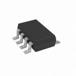
| 描述 | IC DGTL POT 50K UP/DN TSOT23-8数字电位计 IC IC 6-Bit Up/Down |
| 产品分类 | |
| 品牌 | Analog Devices Inc |
| 产品手册 | |
| 产品图片 |
|
| rohs | 符合RoHS无铅 / 符合限制有害物质指令(RoHS)规范要求 |
| 产品系列 | 数字电位计 IC,Analog Devices AD5227BUJZ50-R2- |
| 数据手册 | |
| 产品型号 | AD5227BUJZ50-R2 |
| POT数量 | Single |
| 产品种类 | 数字电位计 IC |
| 供应商器件封装 | TSOT-23-8 |
| 其它名称 | AD5227BUJZ50-R2-ND |
| 包装 | 带卷 (TR) |
| 商标 | Analog Devices |
| 存储器类型 | 易失 |
| 安装类型 | 表面贴装 |
| 安装风格 | SMD/SMT |
| 容差 | 20 % |
| 封装 | Reel |
| 封装/外壳 | SOT-23-8 薄型,TSOT-23-8 |
| 封装/箱体 | TSOT-8 |
| 工作温度 | -40°C ~ 105°C |
| 工作电源电压 | 2.7 V |
| 工厂包装数量 | 250 |
| 弧刷存储器 | Volatile |
| 抽头 | 64 |
| 接口 | 3 线串行(芯片选择,增/减) |
| 数字接口 | Up/Down |
| 最大工作温度 | + 105 C |
| 最小工作温度 | - 40 C |
| 标准包装 | 250 |
| 每POT分接头 | 64 |
| 温度系数 | 标准值 35 ppm/°C |
| 电压-电源 | 2.7 V ~ 5.5 V |
| 电源电压-最大 | 5.5 V |
| 电源电压-最小 | 2.7 V |
| 电源电流 | 0.4 uA |
| 电路数 | 1 |
| 电阻 | 50 kOhms |
| 电阻(Ω) | 50k |
| 系列 | AD5227 |


- 商务部:美国ITC正式对集成电路等产品启动337调查
- 曝三星4nm工艺存在良率问题 高通将骁龙8 Gen1或转产台积电
- 太阳诱电将投资9.5亿元在常州建新厂生产MLCC 预计2023年完工
- 英特尔发布欧洲新工厂建设计划 深化IDM 2.0 战略
- 台积电先进制程称霸业界 有大客户加持明年业绩稳了
- 达到5530亿美元!SIA预计今年全球半导体销售额将创下新高
- 英特尔拟将自动驾驶子公司Mobileye上市 估值或超500亿美元
- 三星加码芯片和SET,合并消费电子和移动部门,撤换高东真等 CEO
- 三星电子宣布重大人事变动 还合并消费电子和移动部门
- 海关总署:前11个月进口集成电路产品价值2.52万亿元 增长14.8%


PDF Datasheet 数据手册内容提取
64-Position Up/Down Control Digital Potentiometer AD5227 FEATURES FUNCTIONAL BLOCK DIAGRAM 64-position digital potentiometer VDD 10 kΩ, 50 kΩ, 100 kΩ end-to-end terminal resistance AD5227 Simple up/down digital or manual configurable control Midscale preset CS A Low potentiometer mode tempco = 10 ppm/°C 6-BIT UP/DOWN U/D CONTROL W LOGIC Low rheostat mode tempco = 35 ppm/°C CLK B Ultralow power, I = 0.4 μA typ and 3 μA max DD Fast adjustment time, ts = 1 μs GND CLAohuwitpo o mspeoleetricavtte ien tnegam vboplelet mraaguteult,r i2ep. l7rea Vdn egtove i,5c −e.54 o 0Vp° Cer taot i+o1n0 5°C MIDPSOCRALE REWGIPISETRER 04419-0-001 Figure 1. Compact thin SOT-23-8 (2.9 mm × 3 mm) Pb-free package APPLICATIONS Mechanical potentiometer and trimmer replacements LCD backlight, contrast, and brightness controls Portable electronics level adjustment Programmable power supply Digital trimmer replacements Automatic closed-loop control GENERAL DESCRIPTION The AD5227 is Analog Devices’ latest 64-step up/down control The AD5227 is available in a compact thin SOT-23-8 (TSOT-8) digital potentiometer1. This device performs the same electronic Pb-free package. The part is guaranteed to operate over the adjustment function as a 5 V potentiometer or variable resistor. automotive temperature range of −40°C to +105°C. Its simple 3-wire up/down interface allows manual switching or Users who consider EEMEM potentiometers should refer to high speed digital control. The AD5227 presets to midscale at some recommendations in the Applications section. power-up. When CS is enabled, the devices changes step at every clock pulse. The direction is determined by the state of Table 1. Truth Table the U/D pin (see Table 1). The interface is simple to activate by CS CLK U/D Operation1 any host controller, discrete logic, or manually with a rotary 0 ↓ 0 RWB Decrement encoder or pushbuttons. The AD5227’s 64-step resolution, small 0 ↓ 1 R Increment WB footprint, and simple interface enable it to replace mechanical 1 X X No Operation potentiometers and trimmers with typically 6× improved resolution, solid-state reliability, and design layout flexibility, 1 RWA increments if RWB decrements and vice versa. resulting in a considerable cost savings in end users’ systems. 1 The terms digital potentiometer and RDAC are used interchangeably. Rev. B Information furnished by Analog Devices is believed to be accurate and reliable. However, no responsibility is assumed by Analog Devices for its use, nor for any infringements of patents or other rights of third parties that may result from its use. One Technology Way, P.O. Box 9106, Norwood, MA 02062-9106, U.S.A. Specifications subject to change without notice. No license is granted by implication or otherwise under any patent or patent rights of Analog Devices. Trademarks and Tel: 781.329.4700 www.analog.com registered trademarks are the property of their respective owners. Fax: 781.326.8703© 2004–2009 Analog Devices, Inc. All rights reserved.
AD5227 TABLE OF CONTENTS Electrical Characteristics ................................................................. 3 Applications ..................................................................................... 12 Interface Timing Diagrams ......................................................... 4 Manual Control with Toggle and Pushbutton Switches ........ 12 Absolute Maximum Ratings ............................................................ 5 Manual Control with Rotary Encoder ..................................... 12 ESD Caution .................................................................................. 5 Adjustable LED Driver .............................................................. 12 Pin Configuration and Function Descriptions ............................. 6 Adjustable Current Source for LED Driver ............................ 12 Typical Performance Characteristics ............................................. 7 Adjustable High Power LED Driver ........................................ 13 Theory of Operation ...................................................................... 10 Automatic LCD Panel Backlight Control ................................ 13 Programming the Digital Potentiometers ............................... 10 6-Bit Controller .......................................................................... 13 Digital Interface .......................................................................... 11 Constant Bias with Supply to Retain Resistance Setting ....... 14 Terminal Voltage Operation Range ......................................... 11 Outline Dimensions ....................................................................... 15 Power-Up and Power-Down Sequences .................................. 11 Ordering Guide .......................................................................... 15 Layout and Power Supply Biasing ............................................ 11 REVISION HISTORY 5/09—Rev. A to Rev. B Changes to Table 2……………………………………………3 4/09—Rev. 0 to Rev. A Changes to Table 2……………………………………………3 Changes to Ordering Guide …………………………………15 3/04—Revision 0: Initial Version Rev. B | Page 2 of 16
AD5227 ELECTRICAL CHARACTERISTICS 10 kΩ, 50 kΩ, 100 kΩ versions: V = 3 V ± 10% or 5 V ± 10%, V = V , V = 0 V, −40°C < T < +105°C, unless otherwise noted. DD A DD B A Table 2. Parameter Symbol Conditions Min Typ1 Max Unit DC CHARACTERISTICS RHEOSTAT MODE Resistor Differential Nonlinearity2 R-DNL R , A = no connect −0.5 ±0.15 +0.5 LSB WB Resistor Integral Nonlinearity2 R-INL R , A = no connect −1 ±0.3 +1 LSB WB Nominal Resistor Tolerance3 ∆R /R −20 +20 % AB AB Resistance Temperature Coefficient (∆R /R )/∆T × 106 35 ppm/°C AB AB Wiper Resistance R V = 2.7 V 100 250 Ω W DD V = 2.8 V to 5.5 V 50 200 Ω DD DC CHARACTERISTICS POTENTIOMETER DIVIDER MODE Resolution N 6 Bits Integral Nonlinearity3 INL −1 ±0.1 +1 LSB Differential Nonlinearity3, 4 DNL −0.5 ±0.1 +0.5 LSB Voltage Divider Temperature Coefficient (∆V /V )/∆T × 106 Midscale 5 ppm/°C W W Full-Scale Error V ≥+31 steps from midscale −1.2 −0.5 0 LSB WFSE −40°C < T < +60°C, −1 −0.5 0 LSB A V = 2.8 V to 5.5 V DD Zero-Scale Error V ≤−32 steps from midscale 0 0.5 1.2 LSB WZSE −40°C < T < +60°C, 0 0.5 1 LSB A V = 2.8 V to 5.5 V DD RESISTOR TERMINALS Voltage Range5 V With respect to GND 0 V V A, B, W DD Capacitance A, B6 C f = 1 MHz, measured to 140 pF A, B GND Capacitance W6 C f = 1 MHz, measured to 150 pF W GND Common-Mode Leakage I V = V = V 1 nA CM A B W DIGITAL INPUTS (CS, CLK, U/D) Input Logic High V 2.4 5.5 V IH Input Logic Low V 0 0.8 V IL Input Current I V = 0 V or 5 V ±1 μA I IN Input Capacitance6 C 5 pF I POWER SUPPLIES Power Supply Range V 2.7 5.5 V DD Supply Current I V = 5 V or V = 0 V, 0.4 3 μA DD IH IL V = 5 V DD Power Dissipation7 P V = 5 V or V = 0 V, 17 μW DISS IH IL V = 5 V DD Power Supply Sensitivity PSSR V = 5 V ± 10% 0.01 0.05 %/% DD DYNAMIC CHARACTERISTICS6, 8, 9 Bandwidth −3 dB BW_10 k R = 10 kΩ, midscale 460 kHz AB BW_50 k R = 50 kΩ, midscale 100 kHz AB BW_100 k R = 100 kΩ, midscale 50 kHz AB Total Harmonic Distortion THD V = 1 V rms, R = 10 kΩ, 0.05 % A AB V = 0 V dc, f = 1 kHz B Adjustment Settling Time t V = 5 V ± 1 LSB error 1 μs S A band, V = 0, measured at B V W Resistor Noise Voltage e R = 5 kΩ, f = 1 kHz 14 nV/√Hz N_WB WB Footnotes on the next page. Rev. B | Page 3 of 16
AD5227 Parameter Symbol Conditions Min Typ1 Max Unit INTERFACE TIMING CHARACTERISTICS (applies to all parts6, 10) Clock Frequency f 50 MHz CLK Input Clock Pulse Width t , t Clock level high or low 10 ns CH CL CS to CLK Setup Time t 10 ns CSS CS Rise to CLK Hold Time t 10 ns CSH U/D to Clock Fall Setup Time t 10 ns UDS 1 Typicals represent average readings at 25°C, VDD = 5 V. 2 Resistor position nonlinearity error, R-INL, is the deviation from an ideal value measured between the maximum resistance and the minimum resistance wiper positions. R-DNL measures the relative step change from ideal between successive tap positions. Parts are guaranteed monotonic. 3 NL and DNL are measured at VW with the RDAC configured as a potentiometer divider similar to a voltage output D/A converter. VA = VDD and VB = 0 V. 4 DNL specification limits of ±1 LSB maximum are guaranteed monotonic operating conditions. 5 Resistor Terminals A, B, W have no limitations on polarity with respect to each other. 6 Guaranteed by design and not subject to production test. 7 PDISS is calculated from (IDD × VDD). CMOS logic level inputs result in minimum power dissipation. 8 Bandwidth, noise, and settling time are dependent on the terminal resistance value chosen. The lowest R value results in the fastest settling time and highest bandwidth. The highest R value results in the minimum overall power consumption. 9 All dynamic characteristics use VDD = V. 10 All input control voltages are specified with tR = tF = 1 ns (10% to 90% of VDD) and timed from a voltage level of 1.6 V. Switching characteristics are measured using VDD = 5 V. INTERFACE TIMING DIAGRAMS CS = LOW U/D = HIGH CLK RWB 04419-0-004 Figure 2. Increment RWB CS = LOW U/D = 0 CLK RWB 04419-0-005 Figure 3. Decrement RWB 1 CS 0 t CSS tCH tCSH t 1 CL CLK 0 t UDS 1 U/D 0 t S RWB 04419-0-006 Figure 4. Detailed Timing Diagram (Only RWB Decrement Shown) Rev. B | Page 4 of 16
AD5227 ABSOLUTE MAXIMUM RATINGS Table 3. Parameter Rating V to GND −0.3 V, +7 V DD V , V , V to GND 0 V, V A B W DD Digital Input Voltage to GND (CS, CLK, U/D) 0 V, V DD Maximum Current I , I Pulsed ±20 mA WB WA I Continuous (R ≤ 5 kΩ, A open)1 ±1 mA Stresses above those listed under Absolute Maximum Ratings WB WB I Continuous (R ≤ 5 kΩ, B open)1 ±1 mA may cause permanent damage to the device. This is a stress WA WA rating only and functional operation of the device at these or I Continuous ±500 μA/ AB (R = 10 kΩ/50 kΩ/100 kΩ)1 ±100 μA/±50 μA any other conditions above those indicated in the operational AB Operating Temperature Range −40°C to +105°C section of this specification is not implied. Exposure to absolute Maximum Junction Temperature (Tmax) 150°C maximum rating conditions for extended periods may affect J Storage Temperature −65°C to +150°C device reliability. Lead Temperature (Soldering, 10 s – 30 s) 245°C Thermal Resistance2 θ 230°C/W JA 1 Maximum terminal current is bounded by the maximum applied voltage across any two of the A, B, and W terminals at a given resistance, the maximum current handling of the switches, and the maximum power dissipation of the package. VDD = 5 V. 2 Package power dissipation = (TJmax – TA) / θJA. ESD CAUTION ESD (electrostatic discharge) sensitive device. Electrostatic charges as high as 4000 V readily accumulate on the human body and test equipment and can discharge without detection. Although this product features proprietary ESD protection circuitry, permanent damage may occur on devices subjected to high energy electrostatic discharges. Therefore, proper ESD precautions are recommended to avoid performance degradation or loss of functionality. Rev. B | Page 5 of 16
AD5227 PIN CONFIGURATION AND FUNCTION DESCRIPTIONS CLK 1 8 VDD AD5227 U/D 2 7 CS TOP VIEW GNDA 34 (Not to Scale) 65 BW 04419-0-003 Figure 5. Pin Configuration Table 4. Pin Function Descriptions Pin No. Mnemonic Description 1 CLK Clock Input. Each clock pulse executes the step-up or step-down of the resistance. The direction is determined by the state of the U/D pin. CLK is a negative-edge trigger. Logic high signal can be higher than V , but lower DD than 5.5 V. 2 U/D Up/Down Selections. Logic 1 selects up and Logic 0 selects down. U can be higher than V , but lower than 5.5 V. DD 3 A Resistor Terminal A. GND ≤ V ≤ V . A DD 4 GND Common Ground. 5 W Wiper Terminal W. GND ≤ V ≤ V . W DD 6 B Resistor Terminal B. GND ≤ V ≤ V . B DD 7 CS Chip Select. Active Low. Logic high signal can be higher than V , but lower than 5.5 V. DD 8 V Positive Power Supply, 2.7 V to 5.5 V. DD Rev. B | Page 6 of 16
AD5227 TYPICAL PERFORMANCE CHARACTERISTICS 0.25 0.25 –40°C –40°C 0.20 +25°C 0.20 +25°C +85°C +85°C 0.15 +105°C SB) 0.15 +105°C LSB) 0.10 VDD = 5.5V NL (L 0.10 VDD = 5.5V E INL ( 0.05 ODE D 0.05 AT MOD–0.050 ETER M–0.050 T M RHEOS––00..1150 TENTIO––00..1150 O ––00..2250 04419-0-007 P––00..2250 04419-0-012 0 8 16 24 32 40 48 56 64 0 8 16 24 32 40 48 56 64 CODE (Decimal) CODE (Decimal) Figure 6. R-INL vs. Code vs. Temperature, VDD = 5 V Figure 9. DNL vs. Code vs. Temperature, VDD = 5 V 0.25 0 –40°C 0.20 +25°C –0.1 +85°C 0.15 +105°C B) VDD = 5.5V –0.2 S L 0.10 L ( –0.3 MODE DN 0.005 E (LSB) ––00..54 VDD = 5.5V AT –0.05 FS ST –0.6 EO–0.10 VDD = 2.7V RH–0.15 –0.7 ––00..2250 04419-0-008 ––00..98 04419-0-013 0 8 16 24 32 40 48 56 64 –40 –20 0 20 40 60 80 100 CODE (Decimal) TEMPERATURE (°C) Figure 7. R-DNL vs. Code vs. Temperature, VDD = 5 V Figure 10. Full-Scale Error vs. Temperature 0.25 1.0 –40°C 0.20 +25°C 0.9 +85°C B) 0.15 +105°C 0.8 L (LS 0.10 VDD = 5.5V 0.7 VDD = 2.7V N ODE I 0.05 B) 0.6 M S TER 0 SE (L 0.5 VDD = 5.5V E–0.05 Z 0.4 M O TI–0.10 0.3 N E OT–0.15 0.2 P––00..2250 04419-0-010 0.10 04419-0-014 0 8 16 24 32 40 48 56 64 –40 –20 0 20 40 60 80 100 CODE (Decimal) TEMPERATURE (°C) Figure 8. INL vs. Code, VDD = 5 V Figure 11. Zero-Scale Error vs. Temperature Rev. B | Page 7 of 16
AD5227 1 20 VDD = 5.5V 1500kkΩΩ C) 15 100kΩ m/° VDD = 5.5V p 10 A)μ O (p URRENT ( E TEMPC 05 C D LY MO –5 PP AT U T S OS –10 E H 0.1 04419-0-015 R ––2105 04419-0-018 –40 –20 0 20 40 60 80 100 0 8 16 24 32 40 48 56 64 TEMPERATURE (°C) CODE (Decimal) Figure 12. Supply Current vs. Temperature Figure 15. Rheostat Mode Tempco ΔRWB/ΔT vs. Code 1 20 VDD = 5.5V C) 1500kkΩΩ RAB = 100kΩ m/° 15 100kΩ )Ω pp VDD = 5.5V R (kAB PCO ( 10 E, EM 5 C T ESISTAN RAB = 50kΩ R MODE 0 R E –5 OMINAL NTIOMET –10 N E 0.1 RAB = 10kΩ 04419-0-016 POT ––2105 04419-0-019 –40 –20 0 20 40 60 80 100 0 8 16 24 32 40 48 56 64 TEMPERATURE (°C) CODE (Decimal) Figure 13. Nominal Resistance vs. Temperature Figure 16. Potentiometer Mode Tempco ΔRWB/ΔT vs. Code 120 REF LEVEL /DIV MARKER 461 441.868Hz 0dB 6.0dB MAG (A/R) –8.957dB 6 VDD = 2.7V TA = 25°C 100 0 VDD = 5.5V )Ω –6 32 STEPS VA = 50mV rms E, R (W 80 –12 16 STEPS C 8 STEPS N –18 TA 60 4 STEPS ESIS VDD = 5.5V dB –24 2 STEPS R R 40 –30 1 STEP E P WI –36 20 0–40 –20 0 20 40 60 80 100 04419-0-017 –––544482 04419-0-042 TEMPERATURE (°C) 1k 10k 100k 1M START 1 000.000Hz STOP 1 000 000.000Hz Figure 14. Wiper Resistance vs. Temperature Figure 17. Gain vs. Frequency vs. Code, RAB = 10 kΩ Rev. B | Page 8 of 16
AD5227 REF LEVEL /DIV MARKER 100 885.289Hz 200 0dB 6.0dB MAG (A/R) –9.060dB 6 TA = 25°C 0 VDD = 5.5V –6 32 STEPS VA = 50mV rms 150 16 STEPS –12 –18 8 STEPS A) B –24 4 STEPS (μDD 100 d I –30 2 STEPS VDD = 5V 1 STEP –36 50 –––544482 04419-0-043 010k 100k 1M VDD = 3V 10M04419-0-024 1k 10k 100k 1M FREQUENCY (Hz) START 1 000.000Hz STOP 1 000 000.000Hz Figure 18. Gain vs. Frequency vs. Code, RAB = 50 kΩ Figure 21. IDD vs. CLK Frequency REF LEVEL /DIV MARKER 52 246.435Hz 1.2 0dB 6.0dB MAG (A/R) –9.139dB A = OPEN 6 TA = 25°C TA = 25°C 0 VDD = 5.5V 1.0 –6 3126 SSTTEEPPSS VA = 50mV rms (mA)X 0.8 RAB = 10kΩ –12 A M 8 STEPS B_ –18 W dB –24 42 SSTTEEPPSS ETICAL I 0.6 –30 R 0.4 1 STEP EO RAB = 50kΩ –36 H T 0.2 –––544482 04419-0-044 00 RAB8 = 100k1Ω6 24 32 40 48 56 6404419-0-025 1k 10k 100k 1M CODE (Decimal) START 1 000.000Hz STOP 1 000 000.000Hz Figure 19. Gain vs. Frequency vs. Code, RAB = 100 kΩ Figure 22. Maximum IWB vs. Code 0 STEP = MIDSCALE, VA = VDD, VB = 0V VB = 0V VA 1 –20 B) d SRR ( STEP N STEP N+1 VW P VDD = 3V DC±10% p-p AC –40 VDD = 5V 2 VA = 5V VB = 0V –60100 1k 10VkDD = 5V DC1±0100k% p-p AC 1M04419-0-023 CH1 2.00V CH2 50.0mV M 400ns A CH2 60.0mV 04419-0-022 FREQUENCY (Hz) T 0.00000s Figure 20. PSRR Figure 23. Step Change Settling Time Rev. B | Page 9 of 16
AD5227 THEORY OF OPERATION The AD5227 is a 64-position 3-terminal digitally controlled The end-to-end resistance, R , has 64 contact points accessed AB potentiometer device. It presets to a midscale at system power- by the wiper terminal, plus the B terminal contact, assuming on. When CS is enabled, changing the resistance settings is that R is used (see Figure 25). Clocking the CLK input steps, WB achieved by clocking the CLK pin. It is negative-edge triggered, RWB by one step. The direction is determined by the state of and the direction of stepping is determined by the state of the U/D pin. The change of RWB can be determined by the number U/D input. When the wiper reaches the maximum or the of clock pulses, provided that the AD5227 has not reached its minimum setting, additional CLK pulses do not change the maximum or minimum scale. ΔRWB can, therefore, be wiper setting. approximated as VDD ⎛ R ⎞ ΔR =±⎜CP× AB +R ⎟ (1) WB W AD5227 ⎝ 64 ⎠ CS A where: 6-BIT UP/DOWN U/D CONTROL W CP is the number of clock pulses. LOGIC CLK R is the end-to-end resistance. B AB R is the wiper resistance contributed by the on-resistance of W GND the internal switch. POR WIPER MIDSCALE REGISTER 04419-0-026 Sreinsicseta innc teh ies lporweseesnt te,n cda roef sthhoeu rleds ibsteo tra skternin tgo al ifminiitt eth we icpuerrr ent Figure 24. Functional Block Diagram flow between W and B in this state to a maximum pulse current of no more than 20 mA. Otherwise, degradation or possible destruction of the internal switches can occur. A RS Similar to the mechanical potentiometer, the resistance of the RDAC between the Wiper W and Terminal A also produces a D0 D1 RS digitally controlled complementary resistance, RWA. When these D2 terminals are used, the B terminal can be opened or shorted to D3 RS D4 W. Similarly, ΔR can be approximated as D5 WA W RDAC RW ⎛ R ⎞ UP/DOWN ΔR =±⎜(64−CP) AB +R ⎟ (2) CTRL AND WA ⎝ 64 W⎠ DECODE RSRS =RAB/64 B 04419-0-027 Equations 1 and 2 do not apply when CP = 0. The typical distribution of the resistance tolerance from device Figure 25. AD5227 Equivalent RDAC Circuit to device is process lot dependent. It is possible to have ±20% PROGRAMMING THE DIGITAL POTENTIOMETERS tolerance. Rheostat Operation Potentiometer Mode Operation If only the W-to-B or W-to-A terminals are used as variable If all three terminals are used, the operation is called resistors, the unused terminal can be opened or shorted with W. potentiometer mode. The most common configuration is the This operation is called rheostat mode and is shown in Figure 26. voltage divider operation as shown in Figure 27. A A A VI A FBigure W26. RheoBstat MWode ConBfiguraWtion04419-0-028 B W VC 04419-0-029 Figure 27. Potentiometer Mode Configuration Rev. B | Page 10 of 16
AD5227 operating voltages. Voltage present on Terminal A, B, or W that The change of V is known provided that the AD5227 has not WB exceeds V by more than 0.5 V is clamped by the diode and, reached the maximum or minimum scale. If one ignores the DD therefore, elevates V . There is no polarity constraint between effect of the wiper resistance, the transfer functions can be DD V , V , and V , but they cannot be higher than V -to- simplified as AB WA WB DD GND. CP ΔV =+ V U/D = 1 (3) POWER-UP AND POWER-DOWN SEQUENCES WB A 64 Because of the ESD protection diodes, it is important to power CP on V before applying any voltage to Terminals A, B, and W. ΔV =− V U/D = 0 (4) DD WB A 64 Otherwise, the diodes are forward-biased such that V can be DD Unlike rheostat mode operation where the absolute tolerance is powered unintentionally and can affect the rest of the system high, potentiometer mode operation yields an almost ratiometric circuit. Similarly, VDD should be powered down last. The ideal function of CP/64 with a relatively small error contributed by power-on sequence is in the following order: GND, VDD, VA/B/W, the R term. The tolerance effect is, therefore, almost canceled. and digital inputs. W Although the thin film step resistor, R, and CMOS switches S VDD resistance, R , have very different temperature coefficients, the W ratiometric adjustment also reduces the overall temperature A coefficient to 5 ppm/°C except at low value codes where R W W dominates. B Potentiometer mode operation includes an op amp gain GND 04419-0-031 configuration among others. The A, W, and B terminals can be Figure 29. Maximum Terminal Voltages Set by VDD and GND input or output terminals and have no polarity constraint LAYOUT AND POWER SUPPLY BIASING provided that |V |, |V |, and |V | do not exceed V -to-GND. AB WA WB DD It is a good practice to use compact, minimum lead length DIGITAL INTERFACE layout design. The leads to the input should be as direct as The AD5227 contains a 3-wire serial input interface. The three possible with a minimum conductor length. Ground paths inputs are clock (CLK), chip select (CS), and up/down control should have low resistance and low inductance. It is also good (U/D). These inputs can be controlled digitally for optimum practice to bypass the power supplies with quality capacitors. speed and flexibility Low ESR (equivalent series resistance) 1 μF to 10 μF tantalum or electrolytic capacitors should be applied at the supplies to When CS is pulled low, a clock pulse increments or decrements minimize any transient disturbance and filter low frequency the up/down counter. The direction is determined by the state ripple. of the U/D pin. When a specific state of the U/D remains, the Figure 30 illustrates the basic supply bypassing configuration device continues to change in the same direction under con- for the AD5227. The ground pin of the AD5227 is a digital secutive clocks until it comes to the end of the resistance ground reference that should be joined to the common ground setting. All digital inputs, CS, CLK, and U/D pins, are protected at a single point to minimize the digital ground bounce. with a series input resistor and a parallel Zener ESD structure as shown in Figure 28. AD5227 1kΩ LOGIC VDD + C2 C1 VDD 10μF 0.1μF Figure 28. Equivalent ESD Protection04419-0-030 D igital Pins GND 04419-0-032 TERMINAL VOLTAGE OPERATION RANGE Figure 30. Power Supply Bypassing The AD5227 is designed with internal ESD protection diodes (Figure 29), but the diodes also set the boundary of the terminal Rev. B | Page 11 of 16
AD5227 APPLICATIONS MANUAL CONTROL WITH TOGGLE AND ADJUSTABLE LED DRIVER PUSHBUTTON SWITCHES The AD5227 can be used in many electronics-level adjustments such as LED drivers for LCD panel backlight control. Figure 33 The AD5227’s simple interface allows it to be used with shows an adjustable LED driver. The AD5227 sets the voltage mechanical switches for simple manual operation. The states of across the white LED D1 for the brightness control. Since U2 the CS and U/D can be selected by toggle switches and the CLK handles up to 250 mA, a typical white LED with V of 3.5 V input can be controlled by a pushbutton switch. Because of the F requires a resistor, R1, to limit the U2 current. This circuit is numerous bounces due to contact closure, the pushbutton simple but not power-efficient, therefore the U2 shutdown pin switch should be debounced by flip-flops or by the ADM812 as can be toggled with a PWM signal to conserve power. shown in Figure 31. 5V 5V C3 AD5227 0.1μF 5V UP/DOWN CS C1 C2 U1 V+ 1μF 0.1μF AD5227 – U/D U2 VCC VDD A W AD8591 R1 MANUALF CigINOuCrReN E3MT1E.R MNOTanLuM aAWRl DPGuMINRTs8DEhH1S B2E uTRttOonT UApC/RDLKoYw En NCoCntOroDl04419-0-033 E R CUCL/SDK 1BG0NkΩD + V–PWSMD 6Ω WLDE1HDIT04419-0-035E Figure 33. Low Cost Adjustable LED Driver Figure 32 shows another way of using AD5227 to emulate ADJUSTABLE CURRENT SOURCE FOR LED DRIVER mechanical potentiometer in a rotary knob operation. The rotary encoder U1 has a C ground terminal and two out-of- Since LED brightness is a function of current rather than phase signals, A and B. When U1 is turned clockwise, a pulse forward voltage, an adjustable current source is preferred over a generated from the B terminal leads a pulse generated from the voltage source as shown in Figure 34. A terminal and vice versa. Signals A and B of U1 pass through a quadrature decoder U2 that translates the phase difference 5V VIN VOUT U2 U1 between A and B of U1 into compatible inputs for U3 AD5227. ADP3333 AD5227 ARM-1.5 Therefore, when B leads A (clockwise), U2 provides the AD5227 with a logic high U/D signal, and vice versa. U2 also filters SD GND 5V CVDSD B W noise, jitter, and other transients as well as debouncing the PWM CLK 10kΩ contact bounces generated by U1. U/D A GND 5V R1 R0.S1EΩT 418kΩ 5V 10kRΩ1 10kRΩ2 QUDAEDCROADTEURRE A1 POTEDNIGTIITOAMLETER U2 U3 V+ – R3 LS7084 AD5227 10kΩ 1 8 1 8 U3 U1 RBIAS CLK CLK VDD AD8591 ROTARY 2 7 2 7 ENCODBCAER 34 VVADSDS X4U/X/DB1 65 34 UAG/1NDD WCBS11 65 BW11 V– + D1 VLID 04419-0-036 RE11CT-V1Y12-EF2CS Figure 34. Adjustable Current Source for LED Driver 04419-0-034 The load current can be found as the VWB of the AD5227 divided by R . Figure 32. Manual Rotary Control SET V I = WB (5) D R SET Rev. B | Page 12 of 16
AD5227 AUTOMATIC LCD PANEL BACKLIGHT CONTROL The U1 ADP3333ARM-1.5 is a 1.5 V LDO that is lifted above or lowered below 0 V. When V of the AD5227 is at minimum, With the addition of a photocell sensor, an automatic brightness WB there is no current through D1, so the GND pin of U1 would be control can be achieved. As shown in Figure 36, the resistance at −1.5 V if U3 were biased with the dual supplies. As a result, of the photocell changes linearly but inversely with the light some of the U2 low resistance steps have no effect on the output output. The brighter the light output, the lower the photocell until the U1 GND pin is lifted above 0 V. When VWB of the resistance and vice versa. The AD5227 sets the voltage level that AD5227 is at its maximum, VOUT becomes VL + VAB, so the U1 is gained up by U2 to drive N1 to a desirable brightness. With the supply voltage must be biased with adequate headroom. photocell acting as the variable feedback resistor, the change in Similarly, a PWM signal can be applied at the U1 shutdown pin the light output changes the R2 resistance, therefore causing U2 for power efficiency. This circuit works well for a single LED. to drive N1 accordingly to regulate the output. This simple low cost implementation of the LED controller can compensate for ADJUSTABLE HIGH POWER LED DRIVER the temperature and aging effects typically found in high power Figure 35 shows a circuit that can drive three to four high power LEDs. Similarly, for power efficiency, a PWM signal can be LEDs. ADP1610 is an adjustable boost regulator that provides applied at the gate of N2 to switch the LED on and off without the voltage headroom and current for the LEDs. The AD5227 any noticeable effect. and the op amp form an average gain of 12 feedback network 5V 5V that servos the R voltage and ADP1610’s FB pin 1.2 V band SET R2 gap reference voltage. As the loop is set, the voltage across R SET R1 D1 is regulated around 0.1 V and adjusted by the digital 1kΩ PHOTOCELL WHITE potentiometer. 5V 5V C3 LED 0.1μF ILED =VRRSET (6) C1μ1F C0.21μF ADU51227 – V+ N1 SET VDD A ADU82591 W 2N7002 RenSEoTu sghho utold l ibmei ts mmaalxl iemnuomug hL EtoD c counrsreernvte. Rpo3w shero ubludt alalsrog eb e used CCSLK 10kΩ + V– SD B iabncy h plioaewrvaaelbrleilnel gwr atitnhhge eAR. D2A 5t wo2 2iRd71e t rro ac ltuiimror, eiatn stt hw aeed LljluE asDst mc cheuanrntr gerniannt ggw eRi t3ihs ipno asnsi ble U/D GND PWM 04419-0-038 Figure 36. Automatic LCD Panel Backlight Control accordingly. 6-BIT CONTROLLER 5V The AD5227 can form a simple 6-bit controller with a clock C2 10μF 13.5kRΩ4 ADPU126I1N0 L101μF generator, a comparator, and some output components. Figure 37 shows a generic 6-bit controller with a comparator that first PWM SD SW VOUT compares the sampling output with the reference level and FB D1 C3 1.2V COMP 10μF outputs either a high or low level to the AD5227 U/D pin. The 100kRΩC SS RTGND AD5227 then changes step at every clock cycle in the direction CC D2 indicated by the U/D state. Although this circuit is not as elegant 390pF CSS 10nF D3 as the one shown in Figure 36, it is self-contained, very easy to C8 5V design, and can adapt to various applications. 0.1μF D4 U3 5V U1 V+ AD5227 + VDD AD8541 CLK – U1 V– – U1 0R.2S5EΩT U/D B ADU83531 OUTPUT LD11––SMLBFR60052250-1L0T01M1R0 AD5227 CS GND + R2 W R1 OP AMP 1.1kΩ B A 100Ω 10kΩ – SAMPLING_OUTPUT Figure 35. Adjustable Current Sourc2e0R f03oΩr LEDs in Series 04419-0-037 COMPUA2RATO+R REF 04419-0-039 Figure 37. 6-Bit Controller Rev. B | Page 13 of 16
AD5227 CONSTANT BIAS WITH SUPPLY TO 3.50 TA = 25°C RETAIN RESISTANCE SETTING 3.49 Users who consider EEMEM potentiometers but cannot justify 3.48 the additional cost and programming for their designs can con- V) 3.47 sider constantly biasing the AD5227 with the supply to retain AGE ( 3.46 the resistance setting as shown in Figure 38. The AD5227 is LT O 3.45 designed specifically with low power to allow power conservation Y V R 3.44 even in battery-operated systems. As shown in Figure 39, a E T similar low power digital potentiometer is biased with a 3.4 V AT 3.43 B 450 mA/hour Li-Ion cell phone battery. The measurement shows 3.42 tphoatte nthtieo dmeevtiecre ids raa ipnrsa cnteigcalilg aibplper pooacwhe rb. eCcaounsseta mntolyst b piaosritnagb lteh e 33..4401 04419-0-041 devices do not require detachable batteries for charging. 0 2 4 6 8 10 12 DAYS Although the resistance setting of the AD5227 is lost when the Figure 39. Battery Consumption Measurement battery needs to be replaced, this event occurs so infrequently that the inconvenience is minimal for most applications. VDD SW1 U1 U2 U3 AD5227 VDD VDD VDD + R RE OW COMPONENT X COMPONENT Y ERY M PO BATTSYSTE – GNDGND GND GND 04419-0-040 Figure 38. Constant Bias AD5227 for Resistance Retention Rev. B | Page 14 of 16
AD5227 OUTLINE DIMENSIONS 2.90 BSC 8 7 6 5 1.60 BSC 2.80 BSC 1 2 3 4 PIN 1 INDICATOR 0.65 BSC 1.95 *0.90 BSC 0.87 0.84 *1.00 MAX 0.20 0.08 0.60 0.10 MAX 00..3282 SEATING 84°° 00..4350 PLANE 0° *COMPLIANT TO JEDEC STANDARDS MO-193-BAWITH THE EXCEPTION OF PACKAGE HEIGHT AND THICKNESS. Figure 40. 8-Lead Thin Small Outline Transistor Package [TSOT] (UJ-8) Dimensions shown in millimeters ORDERING GUIDE Model R 1(kΩ) Temperature Range Package Description Package Option Ordering Quantity Branding AB AD5227BUJZ10-RL72 10 −40°C to +105°C 8-Lead TSOT UJ-8 3000 D3G AD5227BUJZ10-R22 10 −40°C to +105°C 8-Lead TSOT UJ-8 250 D3G AD5227BUJZ50-RL72 50 −40°C to +105°C 8-Lead TSOT UJ-8 3000 D3H AD5227BUJZ50-R22 50 −40°C to +105°C 8-Lead TSOT UJ-8 250 D3H AD5227BUJZ100-RL72 100 −40°C to +105°C 8-Lead TSOT UJ-8 3000 D3J AD5227BUJZ100-R22 100 −40°C to +105°C 8-Lead TSOT UJ-8 250 D3J AD5227EVAL 10 Evaluation Board 1 1 The end-to-end resistance RAB is available in 10 kΩ, 50 kΩ, and 100 kΩ versions. The final three characters of the part number determine the nominal resistance value, for example, 10 kΩ = 10. 2 Z = RoHS Compliant Part. Rev. B | Page 15 of 16
AD5227 NOTES © 2004–2009 Analog Devices, Inc. All rights reserved. Trademarks and registered trademarks are the property of their respective owners. D04419–0–5/09(B) Rev. B | Page 16 of 16