ICGOO在线商城 > 集成电路(IC) > 数据采集 - 数字电位器 > MCP4161-502E/SN

 Datasheet下载
- 型号: MCP4161-502E/SN
- 制造商: Microchip
- 库位|库存: xxxx|xxxx
- 要求:
| 数量阶梯 | 香港交货 | 国内含税 |
| +xxxx | $xxxx | ¥xxxx |
查看当月历史价格
查看今年历史价格
MCP4161-502E/SN产品简介:
ICGOO电子元器件商城为您提供MCP4161-502E/SN由Microchip设计生产,在icgoo商城现货销售,并且可以通过原厂、代理商等渠道进行代购。 MCP4161-502E/SN价格参考。MicrochipMCP4161-502E/SN封装/规格:数据采集 - 数字电位器, Digital Potentiometer 5k Ohm 1 Circuit 257 Taps SPI Interface 8-SOIC。您可以下载MCP4161-502E/SN参考资料、Datasheet数据手册功能说明书,资料中有MCP4161-502E/SN 详细功能的应用电路图电压和使用方法及教程。
Microchip Technology的MCP4161-502E/SN是一款单通道、非易失性数字电位器,属于数据采集类元件。它具有256级电阻抽头调节,可替代传统机械电位器,实现精确的电阻调节。

该器件主要应用于需要精密电阻调节和参数校准的场合,如:

1. 工业控制设备:用于传感器信号调节、增益控制或偏置调整,提高系统精度与稳定性。
2. 电源管理电路:用于调节输出电压或电流,实现对电源系统的精确控制。
3. 测试与测量仪器:在仪表中用于零点校准或量程调节,提升测量准确性。
4. 消费电子产品:如音频设备中的音量调节、显示亮度控制等,提供更稳定、耐用的电子调节方案。
5. 汽车电子:用于车内传感器校准、灯光控制或其他需精确模拟调节的场景。

其封装形式为8引脚SOIC,适合表面贴装工艺,适用于空间受限但要求高可靠性的应用环境。由于其非易失特性,断电后仍能保持设定值,因此特别适用于需要长期稳定运行的系统。
| 参数 | 数值 |
| 产品目录 | 集成电路 (IC)半导体 |
| 描述 | IC POT DGTL SNGL 5K SPI 8SOIC数字电位计 IC Sngl 8B NV SPI Rheo |
| 产品分类 | |
| 品牌 | Microchip Technology |
| 产品手册 | |
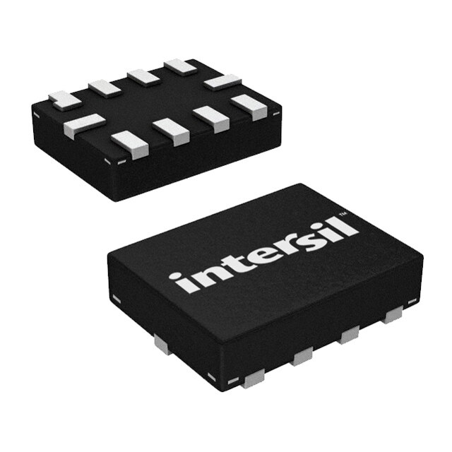
| 产品图片 |
|
| rohs | 符合RoHS无铅 / 符合限制有害物质指令(RoHS)规范要求 |
| 产品系列 | 数字电位计 IC,Microchip Technology MCP4161-502E/SNWiperLock™ |
| 数据手册 | http://www.microchip.com/mymicrochip/filehandler.aspx?ddocname=en531683 |
| 产品型号 | MCP4161-502E/SN |
| PCN组件/产地 | http://www.microchip.com/mymicrochip/NotificationDetails.aspx?id=5774&print=view |
| PCN设计/规格 | http://www.microchip.com/mymicrochip/NotificationDetails.aspx?id=5576&print=viewhttp://www.microchip.com/mymicrochip/NotificationDetails.aspx?id=5704&print=view |
| POT数量 | Single |
| 产品目录页面 | |
| 产品种类 | 数字电位计 IC |
| 供应商器件封装 | 8-SOIC N |
| 其它名称 | MCP4161502ESN |
| 包装 | 管件 |
| 商标 | Microchip Technology |
| 存储器类型 | 非易失 |
| 安装类型 | 表面贴装 |
| 安装风格 | SMD/SMT |
| 封装 | Tube |
| 封装/外壳 | 8-SOIC(0.154",3.90mm 宽) |
| 封装/箱体 | SOIC-8 Narrow |
| 工作温度 | -40°C ~ 125°C |
| 工作电源电压 | 2.5 V, 3.3 V, 5 V |
| 工厂包装数量 | 100 |
| 弧刷存储器 | Non Volatile |
| 抽头 | 257 |
| 接口 | 3 线 SPI(芯片选择) |
| 数字接口 | Serial (4-Wire, SPI) |
| 最大工作温度 | + 125 C |
| 最小工作温度 | - 40 C |
| 标准包装 | 100 |
| 每POT分接头 | 256 |
| 温度系数 | 标准值 150 ppm/°C |
| 电压-电源 | 1.8 V ~ 5.5 V |
| 电源电压-最大 | 5.5 V |
| 电源电压-最小 | 1.8 V |
| 电源电流 | 550 uA |
| 电路数 | 1 |
| 电阻 | 5 kOhms |
| 电阻(Ω) | 5k |


- 商务部:美国ITC正式对集成电路等产品启动337调查
- 曝三星4nm工艺存在良率问题 高通将骁龙8 Gen1或转产台积电
- 太阳诱电将投资9.5亿元在常州建新厂生产MLCC 预计2023年完工
- 英特尔发布欧洲新工厂建设计划 深化IDM 2.0 战略
- 台积电先进制程称霸业界 有大客户加持明年业绩稳了
- 达到5530亿美元!SIA预计今年全球半导体销售额将创下新高
- 英特尔拟将自动驾驶子公司Mobileye上市 估值或超500亿美元
- 三星加码芯片和SET,合并消费电子和移动部门,撤换高东真等 CEO
- 三星电子宣布重大人事变动 还合并消费电子和移动部门
- 海关总署:前11个月进口集成电路产品价值2.52万亿元 增长14.8%


PDF Datasheet 数据手册内容提取
MCP414X/416X/424X/426X 7/8-Bit Single/Dual SPI Digital POT with Non-Volatile Memory Features Description • Single or Dual Resistor Network options The MCP41XX and MCP42XX devices offer a wide • Potentiometer or Rheostat configuration options range of product offerings using an SPI interface. This • Resistor Network Resolution family of devices support 7-bit and 8-bit resistor - 7-bit: 128 Resistors (129 Steps) networks, Non-Volatile memory configurations, and - 8-bit: 256 Resistors (257 Steps) Potentiometer and Rheostat pinouts. • R Resistances options of: AB WiperLock Technology allows application-specific - 5kΩ calibration settings to be secured in the EEPROM. - 10kΩ - 50kΩ Package Types - 100kΩ • Zero-Scale to Full-Scale Wiper operation MCP41X1 MCP41X2 • Low Wiper Resistance: 75Ω (typ.) Single Potentiometer Single Rheostat • Low Tempco: CS 1 8 V CS 1 8 V DD DD - Absolute (Rheostat): 50ppm typical SCK 2 7 P0B SCK 2 7 SDO (0°C to 70°C) SDI/SDO 3 6 P0W SDI 3 6 P0B - Ratiometric (Potentiometer): 15ppm typical VSS 4 5 P0A VSS 4 5 P0W • Non-volatile Memory PDIP, SOIC, MSOP, PDIP, SOIC, MSOP, - Automatic Recall of Saved Wiper Setting 3x3 DFN 3x3 DFN - WiperLock™ Technology MCP42X1 Dual Potentiometers • SPI serial interface (10Mhz, modes 0,0 & 1,1) - High-Speed Read/Writes to wiper registers CS 1 14 VDD SCK 2 13 SDO - Read/Write to Data EEPROM registers SDI 3 12 SHDN - Serially enabled EEPROM write protect VSS 4 11 WP - SDI/SDO multiplexing (MCP41X1 only) P1B 5 10 P0B • Resistor Network Terminal Disconnect Feature P1W 6 9 P0W P1A 7 8 P0A via: PDIP, SOIC, TSSOP - Shutdown pin (SHDN) - Terminal Control (TCON) Register N • Write Protect Feature: S DD DO HD C V S S - Hardware Write Protect (WP) Control pin - Software Write Protect (WP) Configuration bit 16 15 14 13 SCK 1 12 WP • Brown-out reset protection (1.5V typical) • Serial Interface Inactive current (2.5uA typ.) SDI 2 11 NC • High-Voltage Tolerant Digital Inputs: Up to 12.5V VSS 3 10 P0B • Supports Split Rail Applications VSS 4 9 P0W • Internal weak pull-up on all digital inputs 5 6 7 8 • Wide Operating Voltage: B W A A - 2.7V to 5.5V - Device Characteristics P1 P1 P1 P0 Specified 4x4 QFN - 1.8V to 5.5V - Device Operation MCP42X2 Dual Rheostat • Wide Bandwidth (-3dB) Operation: - 2MHz (typ.) for 5.0 kΩ device CS 1 10 VDD SCK 2 9 SDO • Extended temperature range (-40°C to +125°C) SDI 3 8 P0B VSS 4 7 P0W P1B 5 6 P1W MSOP, DFN © 2007 Microchip Technology Inc. DS22059A-page 1
MCP414X/416X/424X/426X Device Block Diagram VDD Power-up/ Resistor P0A Brown-out V Network 0 SS Control (Pot 0) P0W CS SPI Serial Wiper 0 & TCON SCK Interface Register Module & SDI P0B Control SDO Logic (WiperLock™ P1A Resistor WP Technology) Network 1 SHDN (Pot 1) P1W For Dual Potentiometer Wiper 1 Devices Only Memory (16x9) & TCON Wiper0 (V & NV) Register P1B Wiper1 (V & NV) TCON STATUS For Dual Resistor Network Devices Only Data EEPROM (10 x 9-bits) Device Features Device # of POTs ConWfigipuerar tion Control Interface Memory Type WiperLock Technology POR Wiper Setting RARB eOspisttiaonncse ( k(tΩy)picaW-l( )iRΩpW)er # of Steps ORpaeVnrgDaDeti n(2g) MCP4131 (3) 1 Potentiometer (1) SPI RAM No Mid-Scale 5.0, 10.0, 50.0, 100.0 75 129 1.8V to 5.5V MCP4132 (3) 1 Rheostat SPI RAM No Mid-Scale 5.0, 10.0, 50.0, 100.0 75 129 1.8V to 5.5V MCP4141 1 Potentiometer (1) SPI EE Yes NV Wiper 5.0, 10.0, 50.0, 100.0 75 129 2.7V to 5.5V MCP4142 1 Rheostat SPI EE Yes NV Wiper 5.0, 10.0, 50.0, 100.0 75 129 2.7V to 5.5V MCP4151 (3) 1 Potentiometer (1) SPI RAM No Mid-Scale 5.0, 10.0, 50.0, 100.0 75 257 1.8V to 5.5V MCP4152 (3) 1 Rheostat SPI RAM No Mid-Scale 5.0, 10.0, 50.0, 100.0 75 257 1.8V to 5.5V MCP4161 1 Potentiometer (1) SPI EE Yes NV Wiper 5.0, 10.0, 50.0, 100.0 75 257 2.7V to 5.5V MCP4162 1 Rheostat SPI EE Yes NV Wiper 5.0, 10.0, 50.0, 100.0 75 257 2.7V to 5.5V MCP4231 (3) 2 Potentiometer (1) SPI RAM No Mid-Scale 5.0, 10.0, 50.0, 100.0 75 129 1.8V to 5.5V MCP4232 (3) 2 Rheostat SPI RAM No Mid-Scale 5.0, 10.0, 50.0, 100.0 75 129 1.8V to 5.5V MCP4241 2 Potentiometer (1) SPI EE Yes NV Wiper 5.0, 10.0, 50.0, 100.0 75 129 2.7V to 5.5V MCP4242 2 Rheostat SPI EE Yes NV Wiper 5.0, 10.0, 50.0, 100.0 75 129 2.7V to 5.5V MCP4251 (3) 2 Potentiometer (1) SPI RAM No Mid-Scale 5.0, 10.0, 50.0, 100.0 75 257 1.8V to 5.5V MCP4252 (3) 2 Rheostat SPI RAM No Mid-Scale 5.0, 10.0, 50.0, 100.0 75 257 1.8V to 5.5V MCP4261 2 Potentiometer (1) SPI EE Yes NV Wiper 5.0, 10.0, 50.0, 100.0 75 257 2.7V to 5.5V MCP4262 2 Rheostat SPI EE Yes NV Wiper 5.0, 10.0, 50.0, 100.0 75 257 2.7V to 5.5V Note 1: Floating either terminal (A or B) allows the device to be used as a Rheostat (variable resistor). 2: Analog characteristics only tested from 2.7V to 5.5V unless otherwise noted. 3: Please check Microchip web site for device release and availability DS22059A-page 2 © 2007 Microchip Technology Inc.
MCP414X/416X/424X/426X 1.0 ELECTRICAL † Notice: Stresses above those listed under “Maximum Ratings” may cause permanent damage to the device. This is CHARACTERISTICS a stress rating only and functional operation of the device at those or any other conditions above those indicated in the Absolute Maximum Ratings † operational listings of this specification is not implied. Exposure to maximum rating conditions for extended periods Voltage on VDD with respect to VSS............... -0.6V to +7.0V may affect device reliability. Voltage on CS, SCK, SDI, SDI/SDO, WP, and SHDN with respect to V -0.6V to 12.5V SS...................................... Voltage on all other pins (PxA, PxW, PxB, and SDO) with respect to V -0.3V to V + 0.3V SS ............................ DD Input clamp current, I IK (VI < 0, VI > VDD, VI > VPP ON HV pins)......................±20mA Output clamp current, I OK (V < 0 or V > V )..................................................±20mA O O DD Maximum output current sunk by any Output pin ......................................................................................25mA Maximum output current sourced by any Output pin ......................................................................................25mA Maximum current out of V pin.................................100mA SS Maximum current into V pin....................................100mA DD Maximum current into PXA, PXW & PXB pins............±2.5mA Storage temperature ....................................-65°C to +150°C Ambient temperature with power applied -40°C to +125°C Total power dissipation (Note 1)................................400mW Soldering temperature of leads (10 seconds).............+300°C ESD protection on all pins ..................................≥ 4kV (HBM), .......................................................................... ≥ 300V (MM) Maximum Junction Temperature (T ) .........................+150°C J Note 1: Power dissipation is calculated as follows: Pdis = VDD x {IDD - ∑ IOH} + ∑ {(VDD-VOH) x IOH} + ∑(VOl x IOL) © 2007 Microchip Technology Inc. DS22059A-page 3
MCP414X/416X/424X/426X AC/DC CHARACTERISTICS Standard Operating Conditions (unless otherwise specified) Operating Temperature –40°C ≤ T ≤ +125°C (extended) A DC Characteristics All parameters apply across the specified operating ranges unless noted. V = +2.7V to 5.5V, 5kΩ, 10kΩ, 50kΩ, 100kΩ devices. DD Typical specifications represent values for V = 5.5V, T = +25°C. DD A Parameters Sym Min Typ Max Units Conditions Supply Voltage V 2.7 — 5.5 V DD 1.8 — 2.7 V Serial Interface only. CS, SDI, SDO, V V — 12.5V V V ≥ The CS pin will be at one HV SS DD SCK, WP, SHDN 4.5V of three input levels pin Voltage Range (V , V or V ). (Note6) V — V + V V < IL IH IHH SS DD DD 8.0V 4.5V VDD Start Voltage VBOR — — 1.65 V RAM retention voltage (VRAM) < VBOR to ensure Wiper Reset VDD Rise Rate to VDDRR (Note9) V/ms ensure Power-on Reset Delay after device T — 10 20 µS BORD exits the reset state (V > V ) DD BOR Supply Current I — — 450 µA Serial Interface Active, DD (Note10) V = 5.5V, CS = V , SCK @ 5MHz, DD IL write all 0’s to volatile Wiper 0 (address 0h) — — 1 mA EE Write Current, V = 5.5V, CS = V , SCK @ 5MHz, DD IL write all 0’s to non-volatile Wiper 0 (address 2h) — 2.5 5 µA Serial Interface Inactive, CS = V , V = 5.5V IH DD — 0.55 1 mA Serial Interface Active, V = 5.5V, CS = V , DD IHH SCK @ 5MHz, decrement non-volatile Wiper 0 (address 2h) Note 1: Resistance is defined as the resistance between terminal A to terminal B. 2: INL and DNL are measured at V with V = V and V = V . W A DD B SS 3: MCP4XX1 only. 4: MCP4XX2 only, includes V and V . WZSE WFSE 5: Resistor terminals A, W and B’s polarity with respect to each other is not restricted. 6: This specification by design. 7: Non-linearity is affected by wiper resistance (R ), which changes significantly over voltage and W temperature. 8: The MCP4XX1 is externally connected to match the configurations of the MCP41X2 and MCP42X2, and then tested. 9: POR/BOR is not rate dependent. 10: Supply current is independent of current through the resistor network DS22059A-page 4 © 2007 Microchip Technology Inc.
MCP414X/416X/424X/426X AC/DC CHARACTERISTICS (CONTINUED) Standard Operating Conditions (unless otherwise specified) Operating Temperature –40°C ≤ T ≤ +125°C (extended) A DC Characteristics All parameters apply across the specified operating ranges unless noted. V = +2.7V to 5.5V, 5kΩ, 10kΩ, 50kΩ, 100kΩ devices. DD Typical specifications represent values for V = 5.5V, T = +25°C. DD A Parameters Sym Min Typ Max Units Conditions Resistance R 4.0 5 6.0 kΩ -502 devices (Note1) AB (± 20%) 8.0 10 12.0 kΩ -103 devices (Note1) 40.0 50 60.0 kΩ -503 devices (Note1) 80.0 100 120.0 kΩ -104 devices (Note1) Resolution N 257 Taps 8-bit No Missing Codes 129 Taps 7-bit No Missing Codes Step Resistance R — R / — Ω 8-bit Note6 S AB (256) — R / — Ω 7-bit Note6 AB (128) Nominal |R - R | — 0.2 1.25 % MCP42X1 devices only AB0 AB1 Resistance Match / R AB |R - R | — 0.25 1.5 % MCP42X2 devices only, BW0 BW1 / R Code = Full-Scale BW Wiper Resistance R — 75 160 Ω V = 5.5 V, I = 2.0mA, code = 00h W DD W (Note3, Note4) — 75 300 Ω V = 2.7 V, I = 2.0mA, code = 00h DD W Nominal ΔR /ΔT — 50 — ppm/°C T = -20°C to +70°C AB A Resistance — 100 — ppm/°C T = -40°C to +85°C A Tempco — 150 — ppm/°C T = -40°C to +125°C A Ratiometeric ΔV /ΔT — 15 — ppm/°C Code = Midscale (80h or 40h) WB Tempco Resistor Terminal V V V Vss — V V Note5, Note6 A, W, B DD Input Voltage Range (Terminals A, B and W) Maximum current I — — 2.5 mA Note6, Worst case current through W through A, W or B wiper when wiper is either Full Scale or Zero Scale. Leakage current I — 100 — nA MCP4XX1 PxA = PxW = PxB = V WL SS into A, W or B — 100 — nA MCP4XX2 PxB = PxW = V SS Note 1: Resistance is defined as the resistance between terminal A to terminal B. 2: INL and DNL are measured at V with V = V and V = V . W A DD B SS 3: MCP4XX1 only. 4: MCP4XX2 only, includes V and V . WZSE WFSE 5: Resistor terminals A, W and B’s polarity with respect to each other is not restricted. 6: This specification by design. 7: Non-linearity is affected by wiper resistance (R ), which changes significantly over voltage and W temperature. 8: The MCP4XX1 is externally connected to match the configurations of the MCP41X2 and MCP42X2, and then tested. 9: POR/BOR is not rate dependent. 10: Supply current is independent of current through the resistor network © 2007 Microchip Technology Inc. DS22059A-page 5
MCP414X/416X/424X/426X AC/DC CHARACTERISTICS (CONTINUED) Standard Operating Conditions (unless otherwise specified) Operating Temperature –40°C ≤ T ≤ +125°C (extended) A DC Characteristics All parameters apply across the specified operating ranges unless noted. V = +2.7V to 5.5V, 5kΩ, 10kΩ, 50kΩ, 100kΩ devices. DD Typical specifications represent values for V = 5.5V, T = +25°C. DD A Parameters Sym Min Typ Max Units Conditions Full-Scale Error V -6.0 -0.1 — LSb 5kΩ 8-bit 3.0V ≤ V ≤ 5.5V WFSE DD (MCP4XX1 only) -4.0 -0.1 — LSb 7-bit 3.0V ≤ V ≤ 5.5V DD (8-bit code = -3.5 -0.1 — LSb 10kΩ 8-bit 3.0V ≤ V ≤ 5.5V 100h, DD 7-bit code = 80h) -2.0 -0.1 — LSb 7-bit 3.0V ≤ VDD ≤ 5.5V -0.8 -0.1 — LSb 50kΩ 8-bit 3.0V ≤ V ≤ 5.5V DD -0.5 -0.1 — LSb 7-bit 3.0V ≤ V ≤ 5.5V DD -0.5 -0.1 — LSb 100kΩ 8-bit 3.0V ≤ V ≤ 5.5V DD -0.5 -0.1 — LSb 7-bit 3.0V ≤ V ≤ 5.5V DD Zero-Scale Error V — +0.1 +6.0 LSb 5kΩ 8-bit 3.0V ≤ V ≤ 5.5V WZSE DD (MCP4XX1 only) — +0.1 +3.0 LSb 7-bit (8-bit code = 00h, — +0.1 +3.5 LSb 10kΩ 8-bit 3.0V ≤ V ≤ 5.5V 7-bit code = 00h) DD — +0.1 +2.0 LSb 7-bit — +0.1 +0.8 LSb 50kΩ 8-bit 3.0V ≤ V ≤ 5.5V DD — +0.1 +0.5 LSb 7-bit — +0.1 +0.5 LSb 100kΩ 8-bit 3.0V ≤ V ≤ 5.5V DD — +0.1 +0.5 LSb 7-bit Potentiometer INL -1 ±0.5 +1 LSb 8-bit 3.0V ≤ V ≤ 5.5V DD Integral MCP4XX1 devices only -0.5 ±0.25 +0.5 LSb 7-bit Non-linearity (Note2) Potentiometer DNL -0.5 ±0.25 +0.5 LSb 8-bit 3.0V ≤ V ≤ 5.5V DD Differential MCP4XX1 devices only -0.25 ±0.125 +0.25 LSb 7-bit Non-linearity (Note2) Bandwidth -3dB BW — 2 — MHz 5kΩ 8-bit Code = 80h (See Figure2-58, — 2 — MHz 7-bit Code = 40h load = 30pF) — 1 — MHz 10kΩ 8-bit Code = 80h — 1 — MHz 7-bit Code = 40h — 200 — kHz 50kΩ 8-bit Code = 80h — 200 — kHz 7-bit Code = 40h — 100 — kHz 100kΩ 8-bit Code = 80h — 100 — kHz 7-bit Code = 40h Note 1: Resistance is defined as the resistance between terminal A to terminal B. 2: INL and DNL are measured at V with V = V and V = V . W A DD B SS 3: MCP4XX1 only. 4: MCP4XX2 only, includes V and V . WZSE WFSE 5: Resistor terminals A, W and B’s polarity with respect to each other is not restricted. 6: This specification by design. 7: Non-linearity is affected by wiper resistance (R ), which changes significantly over voltage and W temperature. 8: The MCP4XX1 is externally connected to match the configurations of the MCP41X2 and MCP42X2, and then tested. 9: POR/BOR is not rate dependent. 10: Supply current is independent of current through the resistor network DS22059A-page 6 © 2007 Microchip Technology Inc.
MCP414X/416X/424X/426X AC/DC CHARACTERISTICS (CONTINUED) Standard Operating Conditions (unless otherwise specified) Operating Temperature –40°C ≤ T ≤ +125°C (extended) A DC Characteristics All parameters apply across the specified operating ranges unless noted. V = +2.7V to 5.5V, 5kΩ, 10kΩ, 50kΩ, 100kΩ devices. DD Typical specifications represent values for V = 5.5V, T = +25°C. DD A Parameters Sym Min Typ Max Units Conditions Rheostat Integral R-INL -1.5 ±0.5 +1.5 LSb 5kΩ 8-bit 5.5V, I = 900µA W Non-linearity -8.25 +4.5 +8.25 LSb 3.0V, I = 480µA W MCP41X1 (Note7) (Note4, Note8) -1.125 ±0.5 +1.125 LSb 7-bit 5.5V, I = 900µA MCP4XX2 W devices only -6.0 +4.5 +6.0 LSb 3.0V, IW = 480µA (Note4) (Note7) -1.5 ±0.5 +1.5 LSb 10kΩ 8-bit 5.5V, I = 450µA W -5.5 +2.5 +5.5 LSb 3.0V, I = 240µA W (Note7) -1.125 ±0.5 +1.125 LSb 7-bit 5.5V, I = 450µA W -4.0 +2.5 +4.0 LSb 3.0V, I = 240µA W (Note7) -1.5 ±0.5 +1.5 LSb 50kΩ 8-bit 5.5V, I = 90µA W -2.0 +1 +2.0 LSb 3.0V, I = 48µA W (Note7) -1.125 ±0.5 +1.125 LSb 7-bit 5.5V, I = 90µA W -1.5 +1 +1.5 LSb 3.0V, I = 48µA W (Note7) -1.0 ±0.5 +1.0 LSb 100kΩ 8-bit 5.5V, I = 45µA W -1.5 +0.25 +1.5 LSb 3.0V, I = 24µA W (Note7) -0.8 ±0.5 +0.8 LSb 7-bit 5.5V, I = 45µA W -1.125 +0.25 +1.125 LSb 3.0V, I = 24µA W (Note7) Note 1: Resistance is defined as the resistance between terminal A to terminal B. 2: INL and DNL are measured at V with V = V and V = V . W A DD B SS 3: MCP4XX1 only. 4: MCP4XX2 only, includes V and V . WZSE WFSE 5: Resistor terminals A, W and B’s polarity with respect to each other is not restricted. 6: This specification by design. 7: Non-linearity is affected by wiper resistance (R ), which changes significantly over voltage and W temperature. 8: The MCP4XX1 is externally connected to match the configurations of the MCP41X2 and MCP42X2, and then tested. 9: POR/BOR is not rate dependent. 10: Supply current is independent of current through the resistor network © 2007 Microchip Technology Inc. DS22059A-page 7
MCP414X/416X/424X/426X AC/DC CHARACTERISTICS (CONTINUED) Standard Operating Conditions (unless otherwise specified) Operating Temperature –40°C ≤ T ≤ +125°C (extended) A DC Characteristics All parameters apply across the specified operating ranges unless noted. V = +2.7V to 5.5V, 5kΩ, 10kΩ, 50kΩ, 100kΩ devices. DD Typical specifications represent values for V = 5.5V, T = +25°C. DD A Parameters Sym Min Typ Max Units Conditions Rheostat R-DNL -0.5 ±0.25 +0.5 LSb 5kΩ 8-bit 5.5V, I = 900µA W Differential -1.0 +0.5 +1.0 LSb 3.0V (Note7) Non-linearity -0.375 ±0.25 +0.375 LSb 7-bit 5.5V, I = 900µA MCP41X1 W (Note4, Note8) -0.75 +0.5 +0.75 LSb 3.0V (Note7) MCP4XX2 -0.5 ±0.25 +0.5 LSb 10kΩ 8-bit 5.5V, I = 450µA W devices only -1.0 +0.25 +1.0 LSb 3.0V (Note7) (Note4) -0.375 ±0.25 +0.375 LSb 7-bit 5.5V, I = 450µA W -0.75 +0.5 +0.75 LSb 3.0V (Note7) -0.5 ±0.25 +0.5 LSb 50kΩ 8-bit 5.5V, I = 90µA W -0.5 ±0.25 +0.5 LSb 3.0V (Note7) -0.375 ±0.25 +0.375 LSb 7-bit 5.5V, I = 90µA W -0.375 ±0.25 +0.375 LSb 3.0V (Note7) -0.5 ±0.25 +0.5 LSb 100kΩ 8-bit 5.5V, I = 45µA W -0.5 ±0.25 +0.5 LSb 3.0V (Note7) -0.375 ±0.25 +0.375 LSb 7-bit 5.5V, I = 45µA W -0.375 ±0.25 +0.375 LSb 3.0V (Note7) Capacitance (P ) C — 75 — pF f =1MHz, Code = Full-Scale A AW Capacitance (P ) C — 120 — pF f =1MHz, Code = Full-Scale w W Capacitance (P ) C — 75 — pF f =1MHz, Code = Full-Scale B BW Note 1: Resistance is defined as the resistance between terminal A to terminal B. 2: INL and DNL are measured at V with V = V and V = V . W A DD B SS 3: MCP4XX1 only. 4: MCP4XX2 only, includes V and V . WZSE WFSE 5: Resistor terminals A, W and B’s polarity with respect to each other is not restricted. 6: This specification by design. 7: Non-linearity is affected by wiper resistance (R ), which changes significantly over voltage and W temperature. 8: The MCP4XX1 is externally connected to match the configurations of the MCP41X2 and MCP42X2, and then tested. 9: POR/BOR is not rate dependent. 10: Supply current is independent of current through the resistor network DS22059A-page 8 © 2007 Microchip Technology Inc.
MCP414X/416X/424X/426X AC/DC CHARACTERISTICS (CONTINUED) Standard Operating Conditions (unless otherwise specified) Operating Temperature –40°C ≤ T ≤ +125°C (extended) A DC Characteristics All parameters apply across the specified operating ranges unless noted. V = +2.7V to 5.5V, 5kΩ, 10kΩ, 50kΩ, 100kΩ devices. DD Typical specifications represent values for V = 5.5V, T = +25°C. DD A Parameters Sym Min Typ Max Units Conditions Digital Inputs/Outputs (CS, SDI, SDO, SCK, WP, SHDN) Schmitt Trigger V 0.45V — — V 2.7V ≤ V ≤ 5.5V IH DD DD High Input (Allows 2.7V Digital V with DD Threshold 5V Analog V ) DD 0.5V — — V 1.8V ≤ V ≤ 2.7V DD DD Schmitt Trigger V — — 0.2V V IL DD Low Input Threshold Hysteresis of V — 0.1V — V HYS DD Schmitt Trigger Inputs High Voltage Input V 8.5 — 12.5 (6) V Threshold for WiperLock™ Technology IHH Entry Voltage High Voltage Input V — — V + V IHH DD Exit Voltage 0.8V (6) High Voltage Limit V — — 12.5 (6) V Pin can tolerate V or less. MAX MAX Output Low V V — 0.3V V I = 5mA, V = 5.5V OL SS DD OL DD Voltage (SDO) V — 0.3V V I = 1mA, V = 1.8V SS DD OL DD Output High V 0.7V — V V I = -2.5mA, V = 5.5V OH DD DD OH DD Voltage (SDO) 0.7V — V V I = -1mA, V = 1.8V DD DD OL DD Weak Pull-up / I — — 375 uA Internal V pull-up, V pull-down PU DD IHH Pull-down Current — 170 — µA CS pin, V = 5.5V, V = 3V DD CS CS Pull-up / R — 16 — kΩ V = 5.5V, V = 3V CS DD CS Pull-down Resistance Input Leakage I -1 — 1 µA V = V and V = V IL IN DD IN SS Current Pin Capacitance C , C — 10 — pF f = 20MHz IN OUT C RAM (Wiper) Value Value Range N 0h — 1FFh hex 8-bit device 0h — 1FFh hex 7-bit device Note 1: Resistance is defined as the resistance between terminal A to terminal B. 2: INL and DNL are measured at V with V = V and V = V . W A DD B SS 3: MCP4XX1 only. 4: MCP4XX2 only, includes V and V . WZSE WFSE 5: Resistor terminals A, W and B’s polarity with respect to each other is not restricted. 6: This specification by design. 7: Non-linearity is affected by wiper resistance (R ), which changes significantly over voltage and W temperature. 8: The MCP4XX1 is externally connected to match the configurations of the MCP41X2 and MCP42X2, and then tested. 9: POR/BOR is not rate dependent. 10: Supply current is independent of current through the resistor network © 2007 Microchip Technology Inc. DS22059A-page 9
MCP414X/416X/424X/426X AC/DC CHARACTERISTICS (CONTINUED) Standard Operating Conditions (unless otherwise specified) Operating Temperature –40°C ≤ T ≤ +125°C (extended) A DC Characteristics All parameters apply across the specified operating ranges unless noted. V = +2.7V to 5.5V, 5kΩ, 10kΩ, 50kΩ, 100kΩ devices. DD Typical specifications represent values for V = 5.5V, T = +25°C. DD A Parameters Sym Min Typ Max Units Conditions EEPROM Endurance E — 1M — Cycles ndurance EEPROM Range N 0h — 1FFh hex Initial Factory N 80h hex 8-bit WiperLock Technology = Off Setting 40h hex 7-bit WiperLock Technology = Off EEPROM Pro- t — 5 10 ms WC gramming Write Cycle Time Power Requirements Power Supply PSS — 0.0015 0.0035 %/% 8-bit V = 2.7V to 5.5V, DD Sensitivity V = 2.7V, Code = 80h A (MCP41X2 and — 0.0015 0.0035 %/% 7-bit V = 2.7V to 5.5V, DD MCP42X2 only) V = 2.7V, Code = 40h A Note 1: Resistance is defined as the resistance between terminal A to terminal B. 2: INL and DNL are measured at V with V = V and V = V . W A DD B SS 3: MCP4XX1 only. 4: MCP4XX2 only, includes V and V . WZSE WFSE 5: Resistor terminals A, W and B’s polarity with respect to each other is not restricted. 6: This specification by design. 7: Non-linearity is affected by wiper resistance (R ), which changes significantly over voltage and W temperature. 8: The MCP4XX1 is externally connected to match the configurations of the MCP41X2 and MCP42X2, and then tested. 9: POR/BOR is not rate dependent. 10: Supply current is independent of current through the resistor network DS22059A-page 10 © 2007 Microchip Technology Inc.
MCP414X/416X/424X/426X 1.1 SPI Mode Timing Waveforms and Requirements V IHH VIH VIH CS V IL 84 70 72 SCK 83 71 79 78 80 SDO MSb BIT6 - - - - - -1 LSb 75, 76 77 SSDDII MSb IN BIT6 - - - -1 LSb IN 74 73 FIGURE 1-1: SPI Timing Waveform (Mode= 11). TABLE 1-1: SPI REQUIREMENTS (MODE= 11) # Characteristic Symbol Min Max Units Conditions SCK Input Frequency F — 10 MHz V = 2.7V to 5.5V SCK DD — 1 MHz V = 1.8V to 2.7V DD 70 CS Active (V or V ) to SCK↑ input TcsA2scH 60 — ns IL IHH 71 SCK input high time TscH 45 — ns V = 2.7V to 5.5V DD 500 — ns V = 1.8V to 2.7V DD 72 SCK input low time TscL 45 — ns V = 2.7V to 5.5V DD 500 — ns V = 1.8V to 2.7V DD 73 Setup time of SDI input to SCK↑ edge TDIV2scH 10 — ns 74 Hold time of SDI input from SCK↑ edge TscH2DIL 20 — ns 77 CS Inactive (VIH) to SDO output hi-impedance TcsH2DOZ — 50 ns Note1 80 SDO data output valid after SCK↓ edge TscL2DOV — 70 ns VDD = 2.7V to 5.5V 170 ns V = 1.8V to 2.7V DD 83 CS Inactive (V ) after SCK↑ edge TscH2csI 100 — ns V = 2.7V to 5.5V IH DD 1 ms V = 1.8V to 2.7V DD 84 Hold time of CS Inactive (V ) to TcsA2csI 50 — ns IH CS Active (V or V ) IL IHH Note 1: This specification by design. © 2007 Microchip Technology Inc. DS22059A-page 11
MCP414X/416X/424X/426X V IHH VIH VIH 82 CS V IL 84 70 SCK 83 80 71 72 SDO MSb BIT6 - - - - - -1 LSb 75, 76 77 73 SSDDII MSb IN BIT6 - - - -1 LSb IN 74 FIGURE 1-2: SPI Timing Waveform (Mode= 00). TABLE 1-2: SPI REQUIREMENTS (MODE= 00) # Characteristic Symbol Min Max Units Conditions SCK Input Frequency F — 10 MHz V = 2.7V to 5.5V SCK DD — 1 MHz V = 1.8V to 2.7V DD 70 CS Active (V or V ) to SCK↑ input TcsA2scH 60 — ns IL IHH 71 SCK input high time TscH 45 — ns V = 2.7V to 5.5V DD 500 — ns V = 1.8V to 2.7V DD 72 SCK input low time TscL 45 — ns V = 2.7V to 5.5V DD 500 — ns V = 1.8V to 2.7V DD 73 Setup time of SDI input to SCK↑ edge TDIV2scH 10 — ns 74 Hold time of SDI input from SCK↑ edge TscH2DIL 20 — ns 77 CS Inactive (VIH) to SDO output hi-impedance TcsH2DOZ — 50 ns Note 1 80 SDO data output valid after SCK↓ edge TscL2DOV — 70 ns VDD = 2.7V to 5.5V 170 ns V = 1.8V to 2.7V DD 82 SDO data output valid after TssL2doV — 70 ns CS Active (V or V ) IL IHH 83 CS Inactive (V ) after SCK↓ edge TscH2csI 100 — ns V = 2.7V to 5.5V IH DD 1 ms V = 1.8V to 2.7V DD 84 Hold time of CS Inactive (V ) to TcsA2csI 50 — ns IH CS Active (V or V ) IL IHH Note 1: This specification by design. DS22059A-page 12 © 2007 Microchip Technology Inc.
MCP414X/416X/424X/426X TABLE 1-3: SPI REQUIREMENTS FOR SDI/SDO MULTIPLEXED (READ OPERATION ONLY) (2) Characteristic Symbol Min Max Units Conditions SCK Input Frequency F — 250 kHz V = 2.7V to 5.5V SCK DD CS Active (V or V ) to SCK↑ input TcsA2scH 60 — ns IL IHH SCK input high time TscH 1.8 — us SCK input low time TscL 1.8 — ns Setup time of SDI input to SCK↑ edge TDIV2scH 40 — ns Hold time of SDI input from SCK↑ edge TscH2DIL 40 — ns CS Inactive (VIH) to SDO output hi-impedance TcsH2DOZ — 50 ns Note 1 SDO data output valid after SCK↓ edge TscL2DOV — 1.6 us SDO data output valid after TssL2doV — 50 ns CS Active (V or V ) IL IHH CS Inactive (V ) after SCK↓ edge TscH2csI 100 — ns IH Hold time of CS Inactive (V ) to TcsA2csI 50 — ns IH CS Active (V or V ) IL IHH Note 1: This specification by design 2: This table is for the devices where the SPI’s SDI and SDO pins are multiplexed (SDI/SDO) and a Read command is issued. This is NOT required for SDI/SDO operation with the Increment, Decrement, or Write commands. This data rate can be increased by having external pull-up resistors to increase the rising edges of each bit. © 2007 Microchip Technology Inc. DS22059A-page 13
MCP414X/416X/424X/426X TEMPERATURE CHARACTERISTICS Electrical Specifications: Unless otherwise indicated, V =+2.7V to +5.5V, V =GND. DD SS Parameters Sym Min Typ Max Units Conditions Temperature Ranges Specified Temperature Range T -40 — +125 °C A Operating Temperature Range T -40 — +125 °C A Storage Temperature Range T -65 — +150 °C A Thermal Package Resistances Thermal Resistance, 8L-PDIP θ — 84.6 — °C/W JA Thermal Resistance, 8L-SOIC θ — 145.5 — °C/W JA Thermal Resistance, 8L-MSOP θ — 211 — °C/W JA Thermal Resistance, 8L-DFN (3x3) θ — 68.5 — °C/W JA Thermal Resistance, 10L-PDIP θ — 82 — °C/W JA Thermal Resistance, 10L-MSOP θ — 202 — °C/W JA Thermal Resistance, 14L-PDIP θ — 70 — °C/W JA Thermal Resistance, 14L-SOIC θ — 85 — °C/W JA Thermal Resistance, 14L-MSOP θ — N/A — °C/W JA Thermal Resistance, 16L-QFN θ — 50 — °C/W JA DS22059A-page 14 © 2007 Microchip Technology Inc.
MCP414X/416X/424X/426X 2.0 TYPICAL PERFORMANCE CURVES Note: The graphs and tables provided following this note are a statistical summary based on a limited number of samples and are provided for informational purposes only. The performance characteristics listed herein are not tested or guaranteed. In some graphs or tables, the data presented may be outside the specified operating range (e.g., outside specified power supply range) and therefore outside the warranted range. Note: Unless otherwise indicated, T = +25°C, V = 5V, V = 0V. A DD SS 650 250 1000 ) (µA)D 556050000 2222....7777VVVV 128-425505°°°CC°CC 200 680000 ng Current (ID 223344050505000000 5555....5555VVVV 128-425505°°°CC°CC R (kOhms)CS110500 ICS --0244200000000 I (µA)CS Operati 11055000 50 RCS --860000 0 0 -1000 0.00 2.00 4.00 6.00 8.00 10.00 12.00 2 3 4 5 6 7 8 9 10 f (MHz) V (V) SCK CS FIGURE 2-1: Device Current (I ) vs. SPI FIGURE 2-4: CS Pull-up/Pull-down DD Frequency (f ) and Ambient Temperature Resistance (R ) and Current (I ) vs. CS Input SCK CS CS (V = 2.7V and 5.5V). Voltage (V ) (V = 5.5V). DD CS DD 3.0 12 A) stby) (µ 22..05 5.5V old (V) 108 5.5V Entry 2.7V Entry Current (I 11..05 ThreshPP 46 5.5V Exit dby 0.5 2.7V CS V 2 2.7V Exit n a St 0.0 0 -40 25 85 125 -40 -20 0 20 40 60 80 100 120 Ambient Temperature (°C) Ambient Temperature (°C) FIGURE 2-2: Device Current (I ) and FIGURE 2-5: CS High Input Entry/Exit SHDN V . (CS = V ) vs. Ambient Temperature. Threshold vs. Ambient Temperature and V . DD DD DD 900.0 A) µ 800.0 e) ( writ 700.0 nt (I 600.0 e urr 500.0 5.5V C e Writ 400.0 E 300.0 E -40 25 85 125 Ambient Temperature (°C) FIGURE 2-3: Write Current (I ) vs. WRITE Ambient Temperature and V . DD © 2007 Microchip Technology Inc. DS22059A-page 15
MCP414X/416X/424X/426X Note: Unless otherwise indicated, T = +25°C, V = 5V, V = 0V. A DD SS 300 300 0.3 -40C Rw 25C Rw 85C Rw 125C Rw ) W 260 ---444000CCC DRINNwLL 222555CCC IRDNwNLL 888555CCC IRDNwNLL 111222555CCC IRDNwNLL 0.2 ) W 260 --4400CC IDNNLL 2255CC IDNNLL 8855CC IDNNLL 112255CC IDNNLL 6 Wiper Resistance (R(ohms)11120482600000 DNL 85°C12I5N°RLCW --0000.1..21Error (LSb) Wiper Resistance (R(ohms)11120482600000 -40°C RW INL 024 Error (LSb) -40°C 25°C 125°C 85°C25°C DNL 20 -0.3 20 -2 0 32 64 96 128 160 192 224 256 0 32 64 96 128 160 192 224 256 Wiper Setting (decimal) Wiper Setting (decimal) FIGURE 2-6: 5kΩ Pot Mode – R (Ω), FIGURE 2-9: 5kΩ Rheo Mode – R (Ω), W W INL (LSb), DNL (LSb) vs. Wiper Setting and INL (LSb), DNL (LSb) vs. Wiper Setting and Ambient Temperature (V = 5.5V). Ambient Temperature (V = 5.5V). DD DD 120 0.3 120 1.25 -40C Rw 25C Rw 85C Rw 125C Rw -40C Rw 25C Rw 85C Rw 125C Rw R) W 100 --4400CC IDNNLL 2255CC IDNNLL 8855CC IDNNLL 112255CC IDNNLL 0.2 R) W 100 --4400CC DINNLL 2255CC IDNNLL 8855CC IDNNLL 112255CC IDNNLL 0.75 Wiper Resistance ((ohms) 468000 125°C8D5N°CL -40°C 25°CINL RW --0000.1..21Error (LSb) Wiper Resistance ((ohms) 468000 125°C85°C 25°C-40°CINL RW DNL --000.2..72555Error (LSb) 20 -0.3 20 -1.25 0 32 64 96 128 160 192 224 256 0 32 64 96 128 160 192 224 256 Wiper Setting (decimal) Wiper Setting (decimal) FIGURE 2-7: 5kΩ Pot Mode – R (Ω), FIGURE 2-10: 5kΩ Rheo Mode – R (Ω), W W INL (LSb), DNL (LSb) vs. Wiper Setting and INL (LSb), DNL (LSb) vs. Wiper Setting and Ambient Temperature (V = 3.0V). Ambient Temperature (V = 3.0V). DD DD 5300 6000 ) B A 5000 R 5250 al Resistance ((Ohms) 55125000 2.7V R (Ohms)WB234000000000 -40°C n omi 5100 5.5V 1000 2855°°CC N 125°C 5050 0 -40 0 40 80 120 0 32 64 96 128 160 192 224 256 Ambient Temperature (°C) Wiper Setting (decimal) FIGURE 2-8: 5kΩ – Nominal Resistance FIGURE 2-11: 5kΩ – R (Ω) vs. Wiper WB (Ω) vs. Ambient Temperature and V . Setting and Ambient Temperature. DD DS22059A-page 16 © 2007 Microchip Technology Inc.
MCP414X/416X/424X/426X Note: Unless otherwise indicated, T = +25°C, V = 5V, V = 0V. A DD SS FIGURE 2-12: 5kΩ – Low-Voltage FIGURE 2-15: 5kΩ – Low-Voltage Decrement Wiper Settling Time (V = 2.7V) Increment Wiper Settling Time (V = 2.7V) DD DD (1µs/Div). (1µs/Div). FIGURE 2-13: 5kΩ – Low-Voltage FIGURE 2-16: 5kΩ – Low-Voltage Decrement Wiper Settling Time (V = 5.5V) Increment Wiper Settling Time (V = 5.5V) DD DD (1µs/Div). (1µs/Div). FIGURE 2-14: 5kΩ – Power-Up Wiper Response Time (20ms/Div). © 2007 Microchip Technology Inc. DS22059A-page 17
MCP414X/416X/424X/426X Note: Unless otherwise indicated, T = +25°C, V = 5V, V = 0V. A DD SS 120 0.3 120 1 -40C Rw 25C Rw 85C Rw 125C Rw -40C Rw 25C Rw 85C Rw 125C Rw ) W 100 --4400CC IDNNLL 2255CC IDNNLL 8855CC IDNNLL 112255CC IDNNLL 0.2 ) W 100 --4400CC IDNNLL 2255CC IDNNLL 8855CC IDNNLL 112255CC IDNNLL R R 0.5 Wiper Resistance ((ohms) 468000 125°C 85D°CN2L5°C -40°C INL RW --0000.1..21Error (LSb) Wiper Resistance ((ohms) 468000 125°C85°C 25°C -40°INCL RW DNL -00.5Error (LSb) 20 -0.3 20 -1 0 25 50 75 100125150175200225250 0 32 64 96 128 160 192 224 256 Wiper Setting (decimal) Wiper Setting (decimal) FIGURE 2-17: 10kΩ Pot Mode – R (Ω), FIGURE 2-20: 10kΩ Rheo Mode – R (Ω), W W INL (LSb), DNL (LSb) vs. Wiper Setting and INL (LSb), DNL (LSb) vs. Wiper Setting and Ambient Temperature (V = 5.5V). Ambient Temperature (V = 5.5V). DD DD 300 4 300 0.3 -40C Rw 25C Rw 85C Rw 125C Rw -40C Rw 25C Rw 85C Rw 125C Rw -40C INL 25C INL 85C INL 125C INL ) W 260 --4400CC DINNLL 2255CC IDNNLL 8855CC IDNNLL 112255CC IDNNLL 0.2 ) W 260 -40C DNL 25C DNL 85C DNL 125C DNL 3 R R INL Wiper Resistance ((ohms)11120482600000 DNL -40°C IRNWL --0000.1..21Error (LSb) Wiper Resistance ((ohms)11120482600000 -40°C DNL RW -0121 Error (LSb) 125°C 85°C 25°C 125°C 85°C 25°C 20 -0.3 20 -2 0 32 64 96 128 160 192 224 256 0 25 50 75 100125150175200225250 Wiper Setting (decimal) Wiper Setting (decimal) FIGURE 2-18: 10kΩ Pot Mode – R (Ω), FIGURE 2-21: 10kΩ Rheo Mode – R (Ω), W W INL (LSb), DNL (LSb) vs. Wiper Setting and INL (LSb), DNL (LSb) vs. Wiper Setting and Ambient Temperature (V = 3.0V). Ambient Temperature (V = 3.0V). DD DD 10250 12000 ) B A 10000 R 10200 minal Resistance ((Ohms) 111000011505000 5.5V 2.7V R (Ohms)WB 2468000000000000 -284550°°°CCC o N 125°C 10000 0 -40 0 40 80 120 0 32 64 96 128 160 192 224 256 Ambient Temperature (°C) Wiper Setting (decimal) FIGURE 2-19: 10kΩ – Nominal Resistance FIGURE 2-22: 10kΩ – R (Ω) vs. Wiper WB (Ω) vs. Ambient Temperature and V . Setting and Ambient Temperature. DD DS22059A-page 18 © 2007 Microchip Technology Inc.
MCP414X/416X/424X/426X Note: Unless otherwise indicated, T = +25°C, V = 5V, V = 0V. A DD SS FIGURE 2-23: 10kΩ – Low-Voltage FIGURE 2-25: 10kΩ – Low-Voltage Decrement Wiper Settling Time (V = 2.7V) Increment Wiper Settling Time (V = 2.7V) DD DD (1µs/Div). (1µs/Div). FIGURE 2-24: 10kΩ – Low-Voltage FIGURE 2-26: 10kΩ – Low-Voltage Decrement Wiper Settling Time (V = 5.5V) Increment Wiper Settling Time (V = 5.5V) DD DD (1µs/Div). (1µs/Div). © 2007 Microchip Technology Inc. DS22059A-page 19
MCP414X/416X/424X/426X Note: Unless otherwise indicated, T = +25°C, V = 5V, V = 0V. A DD SS 120 0.3 120 0.3 -40C Rw 25C Rw 85C Rw 125C Rw -40C Rw 25C Rw 85C Rw 125C Rw -40C INL 25C INL 85C INL 125C INL -40C INL 25C INL 85C INL 125C INL )W 100 -40C DNL 25C DNL 85C DNL 125C DNL 0.2 )W 100 -40C DNL 25C DNL 85C DNL 125C DNL 0.2 R R INL er Resistance ((ohms) 6800 DNL INL -000.1.1Error (LSb) er Resistance ((ohms) 6800 DNL -000.1.1Error (LSb) Wip 40 25°C -40°C RW -0.2 Wip 40 125°C 85°C 25°C -40°C RW -0.2 125°C 85°C 20 -0.3 20 -0.3 0 32 64 96 128 160 192 224 256 0 32 64 96 128 160 192 224 256 Wiper Setting (decimal) Wiper Setting (decimal) FIGURE 2-27: 50kΩ Pot Mode – R (Ω), FIGURE 2-30: 50kΩ Rheo Mode – R (Ω), W W INL (LSb), DNL (LSb) vs. Wiper Setting and INL (LSb), DNL (LSb) vs. Wiper Setting and Ambient Temperature (V = 5.5V). Ambient Temperature (V = 5.5V). DD DD 300 1 300 0.3 -40C Rw 25C Rw 85C Rw 125C Rw er Resistance (R)W(ohms)111220482600000 ---444000CCCD DRINNNwLLL 222555CCC IRDNwNLL 888IRN555CCCWL IRDNwNLL 111222555CCC IRDNwNLL -0000..12.1Error (LSb) per Resistance (R) W(ohms)111220482600000 --4400CCD DINNNLLL 2255CC IDNNILNLL 88R55CCW IDNNLL 112255CC IDNNLL --000000...257..52555 Error (LSb) Wip 60 -40°C -0.2 Wi 60 -40°C -0.75 125°C 85°C 25°C 125°C 85°C 25°C 20 -0.3 20 -1 0 32 64 96 128 160 192 224 256 0 32 64 96 128 160 192 224 256 Wiper Setting (decimal) Wiper Setting (decimal) FIGURE 2-28: 50kΩ Pot Mode – R (Ω), FIGURE 2-31: 50kΩ Rheo Mode – R (Ω), W W INL (LSb), DNL (LSb) vs. Wiper Setting and INL (LSb), DNL (LSb) vs. Wiper Setting and Ambient Temperature (V = 3.0V). Ambient Temperature (V = 3.0V). DD DD 50800 60000 ) AB 50600 50000 R al Resistance ((Ohms) 45559000802400000000 5.5V 2.7V R (Ohms)WB234000000000000 -40°C n 25°C omi 49600 10000 85°C N 125°C 49400 0 -40 0 40 80 120 0 32 64 96 128 160 192 224 256 Ambient Temperature (°C) Wiper Setting (decimal) FIGURE 2-29: 50kΩ – Nominal Resistance FIGURE 2-32: 50kΩ – R (Ω) vs. Wiper WB (Ω) vs. Ambient Temperature and V . Setting and Ambient Temperature. DD DS22059A-page 20 © 2007 Microchip Technology Inc.
MCP414X/416X/424X/426X Note: Unless otherwise indicated, T = +25°C, V = 5V, V = 0V. A DD SS FIGURE 2-33: 50kΩ – Low-Voltage FIGURE 2-35: 50kΩ – Low-Voltage Decrement Wiper Settling Time (V = 2.7V) Increment Wiper Settling Time (V = 2.7V) DD DD (1µs/Div). (1µs/Div). FIGURE 2-34: 50kΩ – Low-Voltage FIGURE 2-36: 50kΩ – Low-Voltage Decrement Wiper Settling Time (V = 5.5V) Increment Wiper Settling Time (V = 5.5V) DD DD (1µs/Div). (1µs/Div). © 2007 Microchip Technology Inc. DS22059A-page 21
MCP414X/416X/424X/426X Note: Unless otherwise indicated, T = +25°C, V = 5V, V = 0V. A DD SS 120 0.2 120 0.3 -40C Rw 25C Rw 85C Rw 125C Rw -40C Rw 25C Rw 85C Rw 125C Rw ) W 100 --4400CC IDNNLL 2255CC IDNNLL 8855CC IDNNLL 112255CC IDNNLL ) W 100 --4400CC IDNNLL 2255CC IDNNLL 8855CC IDNNLL 112255CC IDNNLL 0.2 R 0.1 R INL er Resistance ((ohms) 6800 DNL INL -00.1Error (LSb) er Resistance ((ohms) 6800 DNL -000.1.1Error (LSb) Wip 40 25°C -40°C RW Wip 40 125°C 85°C 25°C-40°C RW -0.2 125°C 85°C 20 -0.2 20 -0.3 0 32 64 96 128 160 192 224 256 0 32 64 96 128 160 192 224 256 Wiper Setting (decimal) Wiper Setting (decimal) FIGURE 2-37: 100kΩ Pot Mode – R (Ω), FIGURE 2-40: 100kΩ Rheo Mode – R W W INL (LSb), DNL (LSb) vs. Wiper Setting and (Ω), INL (LSb), DNL (LSb) vs. Wiper Setting and Ambient Temperature (V = 5.5V). Ambient Temperature (V = 5.5V). DD DD 300 0.6 300 0.2 -40C Rw 25C Rw 85C Rw 125C Rw -40C Rw 25C Rw 85C Rw 125C Rw -40C INL 25C INL 85C INL 125C INL per Resistance (R) W(ohms)111220482600000 --4400CC IDDNNNLLL 2255CC IDNNLL I88RN55CCLW IDNNLL 112255CC IDNNLL --000000...011..10555Error (LSb) per Resistance (Rw) (ohms)111220482600000 -D40NCL DNL 25C DNINLL 85CR DWNL 125C DNL -0000..24.2 Error (LSb) Wi 60 -40°C -0.15 Wi 60 -40°C -0.4 125°C85°C 25°C 125°C 85°C 25°C 20 -0.2 20 -0.6 0 32 64 96 128 160 192 224 256 0 32 64 96 128 160 192 224 256 Wiper Setting (decimal) Wiper Setting (decimal) FIGURE 2-38: 100kΩ Pot Mode – R (Ω), FIGURE 2-41: 100kΩ Rheo Mode – R W W INL (LSb), DNL (LSb) vs. Wiper Setting and (Ω), INL (LSb), DNL (LSb) vs. Wiper Setting and Ambient Temperature (V = 3.0V). Ambient Temperature (V = 3.0V). DD DD 101500 120000 ) B A 100000 R 101000 al Resistance ((Ohms) 110000050000 2.7V Rwb (Ohms) 468000000000000 -40°C omin 99500 5.5V 20000 2855°°CC N 125°C 99000 0 -40 0 40 80 120 0 32 64 96 128 160 192 224 256 Ambient Temperature (°C) Wiper Setting (decimal) FIGURE 2-39: 100kΩ – Nominal FIGURE 2-42: 100kΩ – R (Ω) vs. Wiper WB Resistance (Ω) vs. Ambient Temperature and Setting and Ambient Temperature. V . DD DS22059A-page 22 © 2007 Microchip Technology Inc.
MCP414X/416X/424X/426X Note: Unless otherwise indicated, T = +25°C, V = 5V, V = 0V. A DD SS M FIGURE 2-43: 100kΩ – Low-Voltage FIGURE 2-45: 100kΩ – Power-Up Wiper Decrement Wiper Settling Time (V = 2.7V) Response Time (1µs/Div). DD (1µs/Div). FIGURE 2-44: 100kΩ – Low-Voltage FIGURE 2-46: 100kΩ – Low-Voltage Decrement Wiper Settling Time (V = 5.5V) Increment Wiper Settling Time (V = 2.7V) DD DD (1µs/Div). (1µs/Div). © 2007 Microchip Technology Inc. DS22059A-page 23
MCP414X/416X/424X/426X Note: Unless otherwise indicated, T = +25°C, V = 5V, V = 0V. A DD SS 0.12 0.1 0.09 0.1 0.08 0.07 0.08 5.5V 0.06 5.5V %0.05 %0.06 0.04 0.04 0.03 3.0V 0.02 0.02 0.01 3.0V 0 0 -40 0 40 80 120 -40 0 40 80 120 Temperature (°C) Temperature (°C) FIGURE 2-47: Resistor Network 0 to FIGURE 2-49: Resistor Network 0 to Resistor Network 1 R (5kΩ) Mismatch vs. V Resistor Network 1 R (50kΩ) Mismatch vs. AB DD AB and Temperature. V and Temperature. DD 0.04 0.05 0.03 0.04 0.02 0.03 5.5V 5.5V 0.01 0.02 % 0 % 0.01 -0.01 0 3.0V 3.0V -0.02 -0.01 -0.03 -0.02 -0.04 -0.03 -40 0 40 80 120 -40 10 60 110 Temperature (°C) Temperature (°C) FIGURE 2-48: Resistor Network 0 to FIGURE 2-50: Resistor Network 0 to Resistor Network 1 R (10kΩ) Mismatch vs. Resistor Network 1 R (100kΩ) Mismatch vs. AB AB V and Temperature. V and Temperature. DD DD DS22059A-page 24 © 2007 Microchip Technology Inc.
MCP414X/416X/424X/426X Note: Unless otherwise indicated, T = +25°C, V = 5V, V = 0V. A DD SS 2.4 0 -5 2.2 5.5V -10 2 -15 2.7V V (V)IH 11..68 (mA)OH --2250 5.5V I -30 1.4 2.7V -35 1.2 -40 1 -45 -40 0 40 80 120 -40 0 40 80 120 Temperature (°C) Temperature (°C) FIGURE 2-51: V (SDI, SCK, CS, WP, and FIGURE 2-53: I (SDO) vs. V and IH OH DD SHDN) vs. V and Temperature. Temperature. DD 1.4 50 1.3 45 5.5V 5.5V 40 1.2 35 V (V)IL 01..191 I (mA)OL 223050 2.7V 15 0.8 2.7V 10 0.7 5 0.6 0 -40 0 40 80 120 -40 0 40 80 120 Temperature (°C) Temperature (°C) FIGURE 2-52: V (SDI, SCK, CS, WP, and FIGURE 2-54: I (SDO) vs. V and IL OL DD SHDN) vs. V and Temperature. Temperature. DD © 2007 Microchip Technology Inc. DS22059A-page 25
MCP414X/416X/424X/426X Note: Unless otherwise indicated, T = +25°C, V = 2.1 Test Circuits A DD 5V, V = 0V. SS 4.2 +5V 4.0 A V s) 3.8 IN W + VOUT m (C 3.6 B - tW 3.4 Offset GND 3.2 2.5V DC 3.0 -40 0 40 80 120 Temperature (°C) FIGURE 2-58: -3db Gain vs. Frequency FIGURE 2-55: Nominal EEPROM Write Test. Cycle Time vs. V and Temperature. DD 1.2 1 5.5V 0.8 V) (D 0.6 2.7V D V 0.4 0.2 0 -40 0 40 80 120 Temperature (°C) FIGURE 2-56: POR/BOR Trip point vs. V DD and Temperature. 15.0 14.5 5.5V z) 14.0 H M 13.5 2.7V k ( c s 13.0 f 12.5 12.0 -40 0 40 80 120 Temperature (°C) FIGURE 2-57: SCK Input Frequency vs. Voltage and Temperature. DS22059A-page 26 © 2007 Microchip Technology Inc.
MCP414X/416X/424X/426X 3.0 PIN DESCRIPTIONS The descriptions of the pins are listed in Table3-1. Additional descriptions of the device pins follows. TABLE 3-1: PINOUT DESCRIPTION FOR THE MCP414X/416X/424X/426X Pin Single Dual Weak Pull-up/ Standard Function Buffer Rheo Pot (1) Rheo Pot Symbol I/O down (2) Type 8L 8L 10L 14L 16L 1 1 1 1 16 CS I HV w/ST “smart” SPI Chip Select Input 2 2 2 2 1 SCK I HV w/ST “smart” SPI Clock Input 3 — 3 3 2 SDI I HV w/ST “smart” SPI Serial Data Input — 3 — — — SDI/SDO (1, 3) I/O HV w/ST “smart” SPI Serial Data Input/Output 4 4 4 4 3, 4 V — P — Ground SS — — 5 5 5 P1B A Analog No Potentiometer 1 Terminal B — — 6 6 6 P1W A Analog No Potentiometer 1 Wiper Terminal — — — 7 7 P1A A Analog No Potentiometer 1 Terminal A — 5 — 8 8 P0A A Analog No Potentiometer 0 Terminal A 5 6 7 9 9 P0W A Analog No Potentiometer 0 Wiper Terminal 6 7 8 10 10 P0B A Analog No Potentiometer 0 Terminal B — — — 11 12 WP I I “smart” Hardware EEPROM Write Protect — — — 12 13 SHDN I HV w/ST “smart” Hardware Shutdown 7 — 9 13 14 SDO O O No SPI Serial Data Out 8 8 10 14 15 V — P — Positive Power Supply Input DD — — — — 11 NC — — — No Connection (4) (4) (4) — (4) Exposed Pad — — — Note4 Legend: HV w/ST = High Voltage tolerant input (with Schmidtt trigger input) A = Analog pins (Potentiometer terminals) I = digital input (high Z) O = digital output I/O = Input / Output P = Power Note 1: The 8-lead Single Potentiometer devices are pin limited so the SDO pin is multiplexed with the SDI pin (SDI/SDO pin). After the Address/Command (first 6-bits) are received, If a valid Read command has been requested, the SDO pin starts driving the requested read data onto the SDI/SDO pin. 2: The pin’s “smart” pull-up shuts off while the pin is forced low. This is done to reduce the standby and shut- down current. 3: The SDO is an open drain output, which uses the internal “smart” pull-up. The SDI input data rate can be at the maximum SPI frequency. the SDO output data rate will be limited by the “speed” of the pull-up, cus- tomers can increase the rate with external pull-up resistors. 4: The DFN and QFN packages have a contact on the bottom of the package. This contact is conductively connected to the die substrate, and therefore should be unconnected or connected to the same ground as the device’s V pin. SS © 2007 Microchip Technology Inc. DS22059A-page 27
MCP414X/416X/424X/426X 3.1 Chip Select (CS) 3.7 Potentiometer Terminal A The CS pin is the serial interface’s chip select input. The terminal A pin is available on the MCP4XX1 Forcing the CS pin to V enables the serial commands. devices, and is connected to the internal potentiome- IL Forcing the CS pin to V enables the high-voltage ter’s terminal A. IHH serial commands. The potentiometer’s terminal A is the fixed connection to the Full Scale wiper value of the digital potentiome- 3.2 Serial Data In (SDI) ter. This corresponds to a wiper value of 0x100 for 8-bit devices or 0x80 for 7-bit devices. The SDI pin is the serial interfaces Serial Data In pin. This pin is connected to the Host Controllers SDO pin. The terminal A pin does not have a polarity relative to the terminal W or B pins. The terminal A pin can 3.3 Serial Data In / Serial Data Out support both positive and negative current. The voltage on terminal A must be between V and V . (SDI/SDO) SS DD The terminal A pin is not available on the MCP4XX2 On the MCP41X1 devices, pin-out limitations do not devices, and the internally terminal A signal is floating. allow for individual SDI and SDO pins. On these MCP42X1 devices have two terminal A pins, one for devices, the SDI and SDO pins are multiplexed. each resistor network. The MCP41X1 serial interface knows when the pin needs to change from being an input (SDI) to being an 3.8 Write Protect (WP) output (SDO). The Host Controller’s SDO pin must be properly protected from a drive conflict. The WP pin is used to force the non-volatile memory to be write protected. 3.4 Ground (V ) SS 3.9 Shutdown (SHDN) The V pin is the device ground reference. SS The SHDN pin is used to force the resistor network 3.5 Potentiometer Terminal B terminals into the hardware shutdown state. The terminal B pin is connected to the internal potenti- 3.10 Serial Data Out (SDO) ometer’s terminal B. The SDO pin is the serial interfaces Serial Data Out pin. The potentiometer’s terminal B is the fixed connection This pin is connected to the Host Controllers SDI pin. to the Zero Scale wiper value of the digital potentiome- ter. This corresponds to a wiper value of 0x00 for both This pin allows the Host Controller to read the digital 7-bit and 8-bit devices. potentiometers registers, or monitor the state of the The terminal B pin does not have a polarity relative to command error bit. the terminal W or A pins. The terminal B pin can support both positive and negative current. The voltage 3.11 Positive Power Supply Input (VDD) on terminal B must be between V and V . SS DD The V pin is the device’s positive power supply input. DD MCP42XX devices have two terminal B pins, one for The input power supply is relative to V . SS each resistor network. While the device V < V (2.7V), the electrical DD min performance of the device may not meet the data sheet 3.6 Potentiometer Wiper (W) Terminal specifications. The terminal W pin is connected to the internal potenti- ometer’s terminal W (the wiper). The wiper terminal is the adjustable terminal of the digital potentiometer. The terminal W pin does not have a polarity relative to terminals A or B pins. The terminal W pin can support both positive and negative current. The voltage on terminal W must be between V and V . SS DD MCP42XX devices have two terminal W pins, one for each resistor network. DS22059A-page 28 © 2007 Microchip Technology Inc.
MCP414X/416X/424X/426X 4.0 FUNCTIONAL OVERVIEW 4.1.2 BROWN-OUT RESET When the device powers down, the device V will This Data Sheet covers a family of thirty-two Digital DD cross the V /V voltage. Potentiometer and Rheostat devices that will be POR BOR referred to as MCP4XXX. The MCP4XX1 devices are Once the V voltage decreases below the V /V DD POR BOR the Potentiometer configuration, while the MCP4XX2 voltage the following happens: devices are the Rheostat configuration. • Serial Interface is disabled As the Device Block Diagram shows, there are four • EEPROM Writes are disabled main functional blocks. These are: If the V voltage decreases below the V voltage DD RAM • POR/BOR Operation the following happens: • Memory Map • Volatile wiper registers may become corrupted • Resistor Network • TCON register may become corrupted • Serial Interface (SPI) As the voltage recovers above the V /V voltage POR BOR The POR/BOR operation and the Memory Map are see Section4.1.1 “Power-on Reset”. discussed in this section and the Resistor Network and Serial commands not completed due to a brown-out SPI operation are described in their own sections. The condition may cause the memory location (volatile and Device Commands commands are discussed in non-volatile) to become corrupted. Section7.0. 4.2 Memory Map 4.1 POR/BOR Operation The device memory is 16 locations that are 9-bits wide The Power-on Reset is the case where the device is (16x9 bits). This memory space contains both volatile having power applied to it from V . The Brown-out SS and non-volatile locations (see Table4-1). Reset occurs when a device had power applied to it, and that power (voltage) drops below the specified TABLE 4-1: MEMORY MAP range. The devices RAM retention voltage (V ) is lower Address Function Memory Type RAM than the POR/BOR voltage trip point (VPOR/VBOR). The 00h Volatile Wiper 0 RAM maximum VPOR/VBOR voltage is less then 1.8V. 01h Volatile Wiper 1 RAM When VPOR/VBOR < VDD < 2.7V, the electrical 02h Non-Volatile Wiper 0 EEPROM performance may not meet the data sheet 03h Non-Volatile Wiper 1 EEPROM specifications. In this region, the device is capable of 04h Volatile TCON Register RAM reading and writing to its EEPROM and incrementing, 05h Status Register RAM decrementing, reading and writing to its volatile memory if the proper serial command is executed. 06h Data EEPROM EEPROM 07h Data EEPROM EEPROM 4.1.1 POWER-ON RESET 08h Data EEPROM EEPROM When the device powers up, the device VDD will cross 09h Data EEPROM EEPROM the V /V voltage. Once the V voltage crosses POR BOR DD 0Ah Data EEPROM EEPROM the V /V voltage the following happens: POR BOR 0Bh Data EEPROM EEPROM • Volatile wiper register is loaded with value in the 0Ch Data EEPROM EEPROM corresponding non-volatile wiper register 0Dh Data EEPROM EEPROM • The TCON register is loaded it’s default value 0Eh Data EEPROM EEPROM • The device is capable of digital operation 0Fh Data EEPROM EEPROM © 2007 Microchip Technology Inc. DS22059A-page 29
MCP414X/416X/424X/426X 4.2.1 NON-VOLATILE MEMORY 4.2.1.4 Special Features (EEPROM) There are 3 non-volatile bits that are not directly This memory can be grouped into two uses of non-vol- mapped into the address space. These bits control the atile memory. These are: following functions: • General Purpose Registers • EEPROM Write Protect • Non-Volatile Wiper Registers • WiperLock Technology for Non-Volatile Wiper 0 The non-volatile wipers starts functioning below the • WiperLock Technology for Non-Volatile Wiper 1 devices V /V trip point. POR BOR The operation of WiperLock Technology is discussed in Section5.3. The state of the WL0, WL1, and WP bits 4.2.1.1 General Purpose Registers is reflected in the STATUS register (see Register4-1). These locations allow the user to store up to 10 (9-bit) locations worth of information. EEPROM Write Protect 4.2.1.2 Non-Volatile Wiper Registers All internal EEPROM memory can be Write Protected. When EEPROM memory is Write Protected, Write These locations contain the wiper values that are commands to the internal EEPROM are prevented. loaded into the corresponding volatile wiper register whenever the device has a POR/BOR event. There are Write Protect (WP) can be enabled/disabled by two up to two registers, one for each resistor network. methods. These are: The non-volatile wiper register enables stand-alone • External WP Hardware pin (MCP42X1 devices operation of the device (without Microcontroller control) only) after being programmed to the desired value. • Non-Volatile configuration bit High Voltage commands are required to enable and 4.2.1.3 Factory Initialization of Non-Volatile disable the nonvolatile WP bit. These commands are Memory (EEPROM) shown in Section7.9 “Modify Write Protect or Wip- The Non-Volatile Wiper values will be initialized to erLock Technology (High Voltage)”. mid-scale value. This is shown in Table4-2. To write to EEPROM, both the external WP pin and the The General purpose EEPROM memory will be internal WP EEPROM bit must be disabled. Write programmed to a default value of 0xFF. Protect does not block commands to the volatile registers. It is good practice in the manufacturing flow to configure the device to your desired settings. 4.2.2 VOLATILE MEMORY (RAM) TABLE 4-2: DEFAULT FACTORY There are four Volatile Memory locations. These are: SETTINGS SELECTION • Volatile Wiper 0 Wiper g • Volatile Wiper 1 Resistance Code Typical R ValueAB Default POR Wiper Setting 8-bCitod7e-bit WiperLock™ Technology and rite Protect Settin ••TrehtST(eeDetn aurtvmtiauoolisln naR aRtveillo eesClg tisaoimstgnoteeetrr m roN( Vlo e(RrtTywAC MosO)rt.kaN rd)ts eR vefiucgenissct teoiornn lyin)g at the RAM W -502 5.0kΩ Mid-scale 80h 40h Disabled -103 10.0kΩ Mid-scale 80h 40h Disabled -503 50.0kΩ Mid-scale 80h 40h Disabled -104 100.0kΩ Mid-scale 80h 40h Disabled DS22059A-page 30 © 2007 Microchip Technology Inc.
MCP414X/416X/424X/426X 4.2.2.1 Status (STATUS) Register STATUS register can be accessed via the READ commands. Register4-1 describes each STATUS This register contains 5 status bits. These bits show the register bit. state of the WiperLock bits, the Shutdown bit the Write Protect bit, and if an EEPROM write cycle is active. The The STATUS register is placed at Address 05h. REGISTER 4-1: STATUS REGISTER R-1 R-1 R-1 R-1 R-0 R-x R-x R-x R-x D8:D5 EEWA WL1 (1) WL0 (1) SHDN WP (1) bit 7 bit 0 Legend: R = Readable bit W = Writable bit U = Unimplemented bit, read as ‘0’ -n = Value at POR ‘1’ = Bit is set ‘0’ = Bit is cleared x = Bit is unknown bit 8-5 D8:D5: Reserved. Forced to “1” bit 4 EEWA: EEPROM Write Active Status bit This bit indicates if the EEPROM Write Cycle is occurring. 1 = An EEPROM Write cycle is currently occurring. Only serial commands to the Volatile memory locations are allowed (addresses 00h, 01h, 04h, and 05h) 0 = An EEPROM Write cycle is NOT currently occurring bit 3 WL1: WiperLock Status bit for Resistor Network 1 (Refer to Section5.3 “WiperLock™ Technology” for further information) WiperLock (WL) prevents the Volatile and Non-Volatile Wiper 1 addresses and the TCON register bits R1HW, R1A, R1W, and R1B from being written to. High Voltage commands are required to enable and disable WiperLock Technology. 1 = Wiper and TCON register bits R1HW, R1A, R1W, and R1B of Resistor Network 1 (Pot 1) are “Locked” (Write Protected) 0 = Wiper and TCON of Resistor Network 1 (Pot 1) can be modified Note: The WL1 bit always reflects the result of the last programming cycle to the non-volatile WL1 bit. After a POR or BOR event, the WL1 bit is loaded with the non-volatile WL1 bit value. bit 2 WL0: WiperLock Status bit for Resistor Network 0 (Refer to Section5.3 “WiperLock™ Technology” for further information) The WiperLock Technology bits (WLx) prevents the Volatile and Non-Volatile Wiper 0 addresses and the TCON register bits R0HW, R0A, R0W, and R0B from being written to. High Voltage commands are required to enable and disable WiperLock Technology. 1 = Wiper and TCON register bits R0HW, R0A, R0W, and R0B of Resistor Network 0 (Pot 0) are “Locked” (Write Protected) 0 = Wiper and TCON of Resistor Network 0 (Pot 0) can be modified Note: The WL0 bit always reflects the result of the last programming cycle to the non-volatile WL0 bit. After a POR or BOR event, the WL0 bit is loaded with the non-volatile WL0 bit value. bit 1 SHDN: Hardware Shutdown pin Status bit (Refer to Section5.4 “Shutdown” for further information) This bit indicates if the Hardware shutdown pin (SHDN) is low. A hardware shutdown disconnects the Terminal A and forces the wiper (Terminal W) to Terminal B (see Figure5-2). While the device is in Hard- ware Shutdown (the SHDN pin is low) the serial interface is operational so the STATUS register may be read. 1 = MCP4XXX is in the Hardware Shutdown state 0 = MCP4XXX is NOT in the Hardware Shutdown state Note 1: Requires a High Voltage command to modify the state of this bit (for Non-Volatile devices only). This bit is Not directly written, but reflects the system state (for this feature). © 2007 Microchip Technology Inc. DS22059A-page 31
MCP414X/416X/424X/426X REGISTER 4-1: STATUS REGISTER (CONTINUED) bit 0 WP: EEPROM Write Protect Status bit (Refer to Section “EEPROM Write Protect” for further infor- mation) This bit indicates the status of the write protection on the EEPROM memory. When Write Protect is enabled, writes to all non-volatile memory are prevented. This includes the General Purpose EEPROM memory, and the non-volatile Wiper registers. Write Protect does not block modification of the volatile wiper register values or the volatile TCON register value (via Increment, Decrement, or Write commands). This status bit is an OR of the devices Write Protect pin (WP) and the internal non-volatile WP bit. High Voltage commands are required to enable and disable the internal WP EEPROM bit. 1 = EEPROM memory is Write Protected 0 = EEPROM memory can be written Note 1: Requires a High Voltage command to modify the state of this bit (for Non-Volatile devices only). This bit is Not directly written, but reflects the system state (for this feature). DS22059A-page 32 © 2007 Microchip Technology Inc.
MCP414X/416X/424X/426X 4.2.2.2 Terminal Control (TCON) Register The value that is written to this register will appear on the resistor network terminals when the serial com- This register contains 8 control bits. Four bits are for mand has completed. Wiper 0, and four bits are for Wiper 1. Register4-2 describes each bit of the TCON register. When the WL1 bit is enabled, writes to the TCON reg- ister bits R1HW, R1A, R1W, and R1B are inhibited. The state of each resistor network terminal connection is individually controlled. That is, each terminal connec- When the WL0 bit is enabled, writes to the TCON reg- tion (A, B and W) can be individually connected/discon- ister bits R0HW, R0A, R0W, and R0B are inhibited. nected from the resistor network. This allows the On a POR/BOR this register is loaded with 1FFh system to minimize the currents through the digital (9-bits), for all terminals connected. The Host Control- potentiometer. ler needs to detect the POR/BOR event and then update the Volatile TCON register value. REGISTER 4-2: TCON BITS (1, 2) R-1 R/W-1 R/W-1 R/W-1 R/W-1 R/W-1 R/W-1 R/W-1 R/W-1 D8 R1HW R1A R1W R1B R0HW R0A R0W R0B bit 8 bit 0 Legend: R = Readable bit W = Writable bit U = Unimplemented bit, read as ‘0’ -n = Value at POR ‘1’ = Bit is set ‘0’ = Bit is cleared x = Bit is unknown bit 8 D8: Reserved. Forced to “1” bit 7 R1HW: Resistor 1 Hardware Configuration Control bit This bit forces Resistor 1 into the “shutdown” configuration of the Hardware pin 1 = Resistor 1 is NOT forced to the hardware pin “shutdown” configuration 0 = Resistor 1 is forced to the hardware pin “shutdown” configuration bit 6 R1A: Resistor 1 Terminal A (P1A pin) Connect Control bit This bit connects/disconnects the Resistor 1 Terminal A to the Resistor 1 Network 1 = P1A pin is connected to the Resistor 1 Network 0 = P1A pin is disconnected from the Resistor 1 Network bit 5 R1W: Resistor 1 Wiper (P1W pin) Connect Control bit This bit connects/disconnects the Resistor 1 Wiper to the Resistor 1 Network 1 = P1W pin is connected to the Resistor 1 Network 0 = P1W pin is disconnected from the Resistor 1 Network bit 4 R1B: Resistor 1 Terminal B (P1B pin) Connect Control bit This bit connects/disconnects the Resistor 1 Terminal B to the Resistor 1 Network 1 = P1B pin is connected to the Resistor 1 Network 0 = P1B pin is disconnected from the Resistor 1 Network bit 3 R0HW: Resistor 0 Hardware Configuration Control bit This bit forces Resistor 0 into the “shutdown” configuration of the Hardware pin 1 = Resistor 0 is NOT forced to the hardware pin “shutdown” configuration 0 = Resistor 0 is forced to the hardware pin “shutdown” configuration bit 2 R0A: Resistor 0 Terminal A (P0A pin) Connect Control bit This bit connects/disconnects the Resistor 0 Terminal A to the Resistor 0 Network 1 = P0A pin is connected to the Resistor 0 Network 0 = P0A pin is disconnected from the Resistor 0 Network Note 1: The hardware SHDN pin (when active) overrides the state of these bits. When the SHDN pin returns to the inactive state, the TCON register will control the state of the terminals. The SHDN pin does not modify the state of the TCON bits. 2: These bits do not affect the wiper register values. © 2007 Microchip Technology Inc. DS22059A-page 33
MCP414X/416X/424X/426X REGISTER 4-2: TCON BITS (1, 2) (CONTINUED) bit 1 R0W: Resistor 0 Wiper (P0W pin) Connect Control bit This bit connects/disconnects the Resistor 0 Wiper to the Resistor 0 Network 1 = P0W pin is connected to the Resistor 0 Network 0 = P0W pin is disconnected from the Resistor 0 Network bit 0 R0B: Resistor 0 Terminal B (P0B pin) Connect Control bit This bit connects/disconnects the Resistor 0 Terminal B to the Resistor 0 Network 1 = P0B pin is connected to the Resistor 0 Network 0 = P0B pin is disconnected from the Resistor 0 Network Note 1: The hardware SHDN pin (when active) overrides the state of these bits. When the SHDN pin returns to the inactive state, the TCON register will control the state of the terminals. The SHDN pin does not modify the state of the TCON bits. 2: These bits do not affect the wiper register values. DS22059A-page 34 © 2007 Microchip Technology Inc.
MCP414X/416X/424X/426X 5.0 RESISTOR NETWORK 5.1 Resistor Ladder Module The Resistor Network has either 7-bit or 8-bit resolu- The resistor ladder is a series of equal value resistors tion. Each Resistor Network allows zero scale to full (RS) with a connection point (tap) between the two scale connections. Figure5-1 shows a block diagram resistors. The total number of resistors in the series for the resistive network of a device. (ladder) determines the RAB resistance (see Figure5-1). The end points of the resistor ladder are The Resistor Network is made up of several parts. connected to analog switches which are connected to These include: the device Terminal A and Terminal B pins. The R AB • Resistor Ladder (and R ) resistance has small variations over voltage S • Wiper and temperature. • Shutdown (Terminal Connections) For an 8-bit device, there are 256 resistors in a string Devices have either one or two resistor networks, between terminal A and terminal B. The wiper can be These are referred to as Pot 0 and Pot 1. set to tap onto any of these 256 resistors thus providing 257 possible settings (including terminal A and terminal A B). For a 7-bit device, there are 128 resistors in a string 8-Bit 7-Bit between terminal A and terminal B. The wiper can be N = N = 257 128 set to tap onto any of these 128 resistors thus providing (100h) (80h) 129 possible settings (including terminal A and terminal R (1) R W B). S 256 127 Equation5-1 shows the calculation for the step resistance. RS RW (1) (FFh) (7Fh) 255 126 EQUATION 5-1: RS CALCULATION (FEh) (7Eh) R (1) R W R RAB S RS = (---2---5A---6-B--)- 8-bit Device W R 1 1 RS = (---1---2A---8-B---)- 7-bit Device (01h) (01h) R (1) R W S 0 0 (00h) (00h) R (1) W Analog Mux B Note1: The wiper resistance is dependent on several factors including, wiper code, device V , Terminal voltages (on A, B, DD and W), and temperature. Also for the same conditions, each tap selection resistance has a small variation. This R variation has greater effects on W some specifications (such as INL) for the smaller resistance devices (5.0kΩ) compared to larger resistance devices (100.0kΩ). FIGURE 5-1: Resistor Block Diagram. © 2007 Microchip Technology Inc. DS22059A-page 35
MCP414X/416X/424X/426X 5.2 Wiper 5.3 WiperLock™ Technology Each tap point (between the R resistors) is a The MCP4XXX device’s WiperLock technology allows S connection point for an analog switch. The opposite application-specific calibration settings to be secured in side of the analog switch is connected to a common the EEPROM without requiring the use of an additional signal which is connected to the Terminal W (Wiper) write-protect pin. There are two WiperLock Technology pin. configuration bits (WL0 and WL1). These bits prevent the Non-Volatile and Volatile addresses and bits for the A value in the volatile wiper register selects which specified resistor network from being written. analog switch to close, connecting the W terminal to the selected node of the resistor ladder. The WiperLock technology prevents the serial commands from doing the following: The wiper can connect directly to Terminal B or to Terminal A. A zero-scale connections, connects the • Changing a volatile wiper value Terminal W (wiper) to Terminal B (wiper setting of • Writing to a non-volatile wiper memory location 000h). A full-scale connections, connects the Terminal • Changing the volatile TCON register value W (wiper) to Terminal A (wiper setting of 100h or 80h). For either Resistor Network 0 or Resistor Network 1 In these configurations the only resistance between the (Potx), the WLx bit controls the following: Terminal W and the other Terminal (A or B) is that of the analog switches. • Non-Volatile Wiper Register • Volatile Wiper Register A wiper setting value greater than full scale (wiper • Volatile TCON register bits RxHW, RxA, RxW, and setting of 100h for 8-bit device or 80h for 7-bit devices) RxB will also be a Full Scale setting (Terminal W (wiper) connected to Terminal A). Table5-1 illustrates the full High Voltage commands are required to enable and wiper setting map. disable WiperLock. Please refer to the Modify Write Protect or WiperLock Technology (High Voltage) Equation5-2 illustrates the calculation used to deter- command for operation. mine the resistance between the wiper and terminal B. 5.3.1 POR/BOR OPERATION WHEN EQUATION 5-2: RWB CALCULATION WIPERLOCK TECHNOLOGY ENABLED R N R = ----A----B------+R 8-bit Device WB (256) W The WiperLock Technology state is not affected by a POR/BOR event. A POR/BOR event will load the N = 0 to 256 (decimal) Volatile Wiper register value with the Non-Volatile R N Wiper register value, refer to Section4.1. R = ----A----B------+R 7-bit Device WB (128) W N = 0 to 128 (decimal) TABLE 5-1: VOLATILE WIPER VALUE VS. WIPER POSITION MAP Wiper Setting Properties 7-bit Pot 8-bit Pot 3FFh 3FFh Reserved (Full Scale (W = A)), 081h 101h Increment and Decrement commands ignored 080h 100h Full Scale (W = A), Increment commands ignored 07Fh 0FFh W = N 041h 081 040h 080h W = N (Mid-Scale) 03Fh 07Fh W = N 001h 001 000h 000h Zero Scale (W = B) Decrement command ignored DS22059A-page 36 © 2007 Microchip Technology Inc.
MCP414X/416X/424X/426X 5.4 Shutdown 5.4.2 TERMINAL CONTROL REGISTER (TCON) Shutdown is used to minimize the device’s current consumption. The MCP4XXX has two methods to The Terminal Control (TCON) register is a volatile achieve this. These are: register used to configure the connection of each resistor network terminal pin (A, B, and W) to the • Hardware Shutdown Pin (SHDN) Resistor Network. This register is shown in • Terminal Control Register (TCON) Register4-2. The Hardware Shutdown pin is backwards compatible The RxHW bits forces the selected resistor network with the MCP42XXX devices. into the same state as the SHDN pin. Alternate low power configurations may be achieved with the RxA, 5.4.1 HARDWARE SHUTDOWN PIN RxW, and RxB bits. (SHDN) Note: When the RxHW bit forces the resistor The SHDN pin is available on the dual potentiometer network into the hardware SHDN state, devices. When the SHDN pin is forced active (V ): IL the state of the TCON register RxA, RxW, • The P0A and P1A terminals are disconnected and RxB bits is overridden (ignored). • The P0W and P1W terminals are simultaneously When the state of the RxHW bit no longer connect to the P0B and P1B terminals, respec- forces the resistor network into the hard- tively (see Figure5-2) ware SHDN state, the TCON register RxA, • The Serial Interface is NOT disabled, and all RxW, and RxB bits return to controlling the Serial Interface activity is executed terminal connection state. In other words, • Any EEPROM write cycles are completed the RxHW bit does not corrupt the state of the RxA, RxW, and RxB bits. The Hardware Shutdown pin mode does NOT corrupt the values in the Volatile Wiper Registers nor the 5.4.3 INTERACTION OF SHDN PIN AND TCON register. When the Shutdown mode is exited TCON REGISTER (SHDN pin is inactive (V )): IH • The device returns to the Wiper setting specified Figure5-3 shows how the SHDN pin signal and the by the Volatile Wiper value RxHW bit signal interact to control the hardware • The TCON register bits return to controlling the shutdown of each resistor network (independently). Using the TCON bits allows each resistor network (Pot terminal connection state 0 and Pot 1) to be individually “shutdown” while the A hardware pin forces both resistor networks to be “shut- down” at the same time. k or w W et N SHDN (from pin) or To Pot x Hardware st RxHW Shutdown Control si e (from TCON register) R B FIGURE 5-2: Hardware Shutdown FIGURE 5-3: RxHW bit and SHDN pin Resistor Network Configuration. Interaction. © 2007 Microchip Technology Inc. DS22059A-page 37
MCP414X/416X/424X/426X NOTES: DS22059A-page 38 © 2007 Microchip Technology Inc.
MCP414X/416X/424X/426X 6.0 SERIAL INTERFACE (SPI) Typical SPI Interfaces are shown in Figure6-1. In the SPI interface, The Master’s Output pin is connected to The MCP4XXX devices support the SPI serial protocol. the Slave’s Input pin and the Master’s Input pin is This SPI operates in the slave mode (does not connected to the Slave’s Output pin. generate the serial clock). The MCP4XXX SPI’s module supports two (of the four) The SPI interface uses up to four pins. These are: standard SPI modes. These are Mode 0,0 and 1,1. • CS - Chip Select The SPI mode is determined by the state of the SCK • SCK - Serial Clock pin (VIH or VIL) on the when the CS pin transitions from • SDI - Serial Data In inactive (VIH) to active (VIL or VIHH). • SDO - Serial Data Out All SPI interface signals are high-voltage tolerant. Typical SPI Interface Connections Host MCP4XXX Controller SDO ( Master Out - Slave In (MOSI) ) SDI SDI ( Master In - Slave Out (MISO) ) SDO SCK SCK I/O (1) CS Typical MCP41X1 SPI Interface Connections (Host Controller Hardware SPI) Host MCP41X1 Controller SDO SDI/SDO SDI 200kΩ SDI SDO SCK SCK I/O (1) CS Alternate MCP41X1 SPI Interface Connections (Host Controller Firmware SPI) Host MCP41X1 Controller I/O SDI/SDO SDI (SDO/SDI) SDO I/O SCK (SCK) I/O (1) CS Note1: If High voltage commands are desired, some type of external circuitry needs to be implemented. FIGURE 6-1: Typical SPI Interface Block Diagram. © 2007 Microchip Technology Inc. DS22059A-page 39
MCP414X/416X/424X/426X 6.1 SDI, SDO, SCK, and CS Operation 6.1.3 SDI/SDO The operation of the four SPI interface pins are Note: MCP41X1 Devices Only . discussed in this section. These pins are: For device packages that do not have enough pins for • SDI (Serial Data In) both an SDI and SDO pin, the SDI and SDO function- • SDO (Serial Data Out) ality is multiplexed onto a single I/O pin called SDI/ • SCK (Serial Clock) SDO. • CS (Chip Select) The SDO will only be driven for the command error bit The serial interface works on either 8-bit or 16-bit (CMDERR) and during the data bits of a read command boundaries depending on the selected command. The (after the memory address and command has been Chip Select (CS) pin frames the SPI commands. received). 6.1.1 SERIAL DATA IN (SDI) 6.1.3.1 SDI/SDO Operation The Serial Data In (SDI) signal is the data signal into Figure6-2 shows a block diagram of the SDI/SDO pin. the device. The value on this pin is latched on the rising The SDI signal has an internal “smart” pull-up. The edge of the SCK signal. value of this pull-up determines the frequency that data can be read from the device. An external pull-up can be 6.1.2 SERIAL DATA OUT (SDO) added to the SDI/SDO pin to improve the rise time and therefore improve the frequency that data can be read. The Serial Data Out (SDO) signal is the data signal out of the device. The value on this pin is driven on the Note: To support the High voltage requirement of falling edge of the SCK signal. the SDI function, the SDO function is an Once the CS pin is forced to the active level (V or open drain output. IL VIHH), the SDO pin will be driven. The state of the SDO Data written on the SDI/SDO pin can be at the pin is determined by the serial bit’s position in the maximum SPI frequency. command, the command selected, and if there is a Note: Care must be take to ensure that a Drive command error state (CMDERR). conflict does not exist between the Host Controllers SDO pin (or software SDI/SDO pin) and the MCP41x1 SDI/SDO pin (see Figure6-1). On the falling edge of the SCK pin during the C0 bit (see Figure7-1), the SDI/SDO pin will start outputting the SDO value. The SDO signal overrides the control of the smart pull-up, such that whenever the SDI/SDO pin is outputting data, the smart pull-up is enabled. The SDI/SDO pin will change from an input (SDI) to an output (SDO) after the state machine has received the Address and Command bits of the Command Byte. If the command is a Read command, then the SDI/SDO pin will remain an output for the remainder of the command. For any other command, the SDI/SDO pin returns to an input. “smart” pull-up SDI/SDO SDI Open drain Control SDO Logic FIGURE 6-2: Serial I/O Mux Block Diagram. DS22059A-page 40 © 2007 Microchip Technology Inc.
MCP414X/416X/424X/426X 6.1.4 SERIAL CLOCK (SCK) 6.1.5 THE CS SIGNAL (SPI FREQUENCY OF OPERATION) The Chip Select (CS) signal is used to select the device The SPI interface is specified to operate up to 10MHz. and frame a command sequence. To start a command, The actual clock rate depends on the configuration of or sequence of commands, the CS signal must the system and the serial command used. Table6-1 transition from the inactive state (VIH) to an active state shows the SCK frequency for different configurations. (VIL or VIHH). After the CS signal has gone active, the SDO pin is TABLE 6-1: SCK FREQUENCY driven and the clock bit counter is reset. Command Note: There is a required delay after the CS pin goes active to the 1st edge of the SCK pin. Memory Type Access Write, Read Increment, If an error condition occurs for an SPI command, then Decrement the Command byte’s Command Error (CMDERR) bit Non-Volatile SDI, SDO 10MHz 10MHz (2, 3) (on the SDO pin) will be driven low (VIL). To exit the Memory SDI/SDO 250kHz (4) 10MHz (2, 3) error condition, the user must take the CS pin to the VIH (1) level. Volatile SDI, SDO 10MHz 10MHz When the CS pin returns to the inactive state (VIH) the Memory SDI/SDO 250kHz (4) 10MHz SPI module resets (including the address pointer). (1) While the CS pin is in the inactive state (VIH), the serial interface is ignored. This allows the Host Controller to Note1: MCP41X1 devices only interface to other SPI devices using the same SDI, 2: Non-Volatile memory does not support SDO, and SCK signals. the Increment or Decrement command. The CS pin has an internal pull-up resistor. The resistor 3: After a Write command, the internal write is disabled when the voltage on the CS pin is at the V IL cycle must complete before the next SPI level. This means that when the CS pin is not driven, command is received. the internal pull-up resistor will pull this signal to the V IH level. When the CS pin is driven low (V ), the resis- 4: This is the maximum clock frequency IL tance becomes very large to reduce the device current without an external pull-up resistor. consumption. The high voltage capability of the CS pin allows High Voltage commands. High Voltage commands allow the device’s WiperLock Technology and write protect features to be enabled and disabled. © 2007 Microchip Technology Inc. DS22059A-page 41
MCP414X/416X/424X/426X 6.2 The SPI Modes 6.3 SPI Waveforms The SPI module supports two (of the four) standard SPI Figure6-3 through Figure6-8 show the different SPI modes. These are Mode 0,0 and 1,1. The mode is command waveforms. Figure6-3 and Figure6-4 are determined by the state of the SDI pin on the rising read and write commands. Figure6-5 and Figure6-6 edge of the 1st clock bit (of the 8-bit byte). are read commands when the SDI and SDO pins are multiplexed on the same pin (SDI/SDO). Figure6-7 6.2.1 MODE 0,0 and Figure6-8 are increment and decrement In Mode 0,0: SCK idle state = low (V ), data is clocked commands. The high voltage increment and decrement IL in on the SDI pin on the rising edge of SCK and clocked commands are used to enable and disable WiperLock out on the SDO pin on the falling edge of SCK. Technology and Write Protect. 6.2.2 MODE 1,1 In Mode 1,1: SCK idle state = high (V ), data is IH clocked in on the SDI pin on the rising edge of SCK and clocked out on the SDO pin on the falling edge of SCK. VIH VIHH CS VIL SCK Write to SSPBUF CMDERR bit SDO bit15 bit14 bit13 bit12 bit11 bit10 bit9 bit8 bit7 bit6 bit5 bit4 bit3 bit2 bit1 bit0 AD3 AD2 AD1 AD0 X D8 D7 D6 D5 D4 D3 D2 D1 D0 SDI bit15 bit14 bit13 bit12 C1 C0 bit9 bit8 bit7 bit6 bit5 bit4 bit3 bit2 bit1 bit0 Input Sample FIGURE 6-3: 16-Bit Commands (Write, Read) - SPI Waveform (Mode 1,1). VIH VIHH CS VIL SCK Write to SSPBUF CMDERR bit SDO bit15 bit14 bit13 bit12 bit11 bit10 bit9 bit8 bit7 bit6 bit5 bit4 bit3 bit2 bit1 bit0 AD3 AD2 AD1 AD0 X D8 D7 D6 D5 D4 D3 D2 D1 D0 SDI bit15 bit14 bit13 bit12 C1 C0 bit9 bit8 bit7 bit6 bit5 bit4 bit3 bit2 bit1 bit0 Input Sample FIGURE 6-4: 16-Bit Commands (Write, Read) - SPI Waveform (Mode 0,0). DS22059A-page 42 © 2007 Microchip Technology Inc.
MCP414X/416X/424X/426X VIH VIHH CS VIL SCK Write to SSPBUF CMDERR bit D9 D8 D7 D6 D5 D4 D3 D2 D1 D0 SDO bit9 bit8 bit7 bit6 bit5 bit4 bit3 bit2 bit1 bit0 AD3 AD2 AD1 AD0 C1 C0 (1) (1) (1) (1) (1) (1) (1) (1) (1) (1) SDI bit15 bit14 bit13 bit12 1 1 Input Sample Note 1: The SDI pin will read the state of the SDI pin which will be the SDO signal, unless overdriven FIGURE 6-5: 16-Bit Read Command for Devices with SDI/SDO multiplexed - SPI Waveform (Mode 1,1). VIH VIHH CS VIL SCK Write to SSPBUF CMDERR bit X D8 D7 D6 D5 D4 D3 D2 D1 D0 SDO bit9 bit8 bit7 bit6 bit5 bit4 bit3 bit2 bit1 bit0 AD3 AD2 AD1 AD0 C1 C0 (1) (1) (1) (1) (1) (1) (1) (1) (1) (1) SDI bit15 bit14 bit13 bit12 1 1 Input Sample Note 1: The SDI pin will read the state of the SDI pin which will be the SDO signal, unless overdriven FIGURE 6-6: 16-Bit Read Command for Devices with SDI/SDO multiplexed - SPI Waveform (Mode 0,0). © 2007 Microchip Technology Inc. DS22059A-page 43
MCP414X/416X/424X/426X CS VIH VIHH VIL SCK Write to SSPBUF CMDERR bit “1” = “Valid” Command/Address “0” = “Invalid” Command/Address SDO bit7 bit6 bit5 bit4 bit3 bit2 bit1 bit0 SDI AD3 AD2 AD1 AD0 C1 C0 X X bit7 bit0 Input Sample FIGURE 6-7: 8-Bit Commands (Increment, Decrement, Modify Write Protect or WiperLock Technology) - SPI Waveform with PIC MCU (Mode 1,1). VIH VIHH CS VIL SCK Write to SSPBUF CMDERR bit “1” = “Valid” Command/Address “0” = “Invalid” Command/Address SDO bit7 bit6 bit5 bit4 bit3 bit2 bit1 bit0 SDI AD3 AD2 AD1 AD0 C1 C0 X X bit7 bit0 Input Sample FIGURE 6-8: 8-Bit Commands (Increment, Decrement, Modify Write Protect or WiperLock Technology) - SPI Waveform with PIC MCU (Mode 0,0). DS22059A-page 44 © 2007 Microchip Technology Inc.
MCP414X/416X/424X/426X 7.0 DEVICE COMMANDS 7.1 Command Byte The MCP4XXX’s SPI command format supports 16 The Command Byte has three fields, the Address, the memory address locations and four commands. Each Command, and 2 Data bits, see Figure7-1. Currently command has two modes. These are: only one of the data bits is defined (D8). This is for the Write command. • Normal Serial Commands • High-Voltage Serial Commands The device memory is accessed when the master sends a proper Command Byte to select the desired Normal serial commands are those where the CS pin is operation. The memory location getting accessed is driven to V . With High-Voltage Serial Commands, the IL contained in the Command Byte’s AD3:AD0 bits. The CS pin is driven to V . In each mode, there are four IHH action desired is contained in the Command Byte’s possible commands. These commands are shown in C1:C0 bits, see Table7-1. C1:C0 determines if the Table7-1. desired memory location will be read, written, The 8-bit commands (Increment Wiper and Decre- Incremented (wiper setting +1) or Decremented (wiper ment Wiper commands) contain a Command Byte, setting -1). The Increment and Decrement commands see Figure7-1, while 16-bit commands (Read Data are only valid on the volatile wiper registers, and in and Write Data commands) contain a Command Byte High Voltage commands to enable/disable WiperLock and a Data Byte. The Command Byte contains two data Technology and Software Write Protect. bits, see Figure7-1. As the Command Byte is being loaded into the device Table7-2 shows the supported commands for each (on the SDI pin), the device’s SDO pin is driving. The memory location and the corresponding values on the SDO pin will output high bits for the first six bits of that SDI and SDO pins. command. On the 7th bit, the SDO pin will output the Table7-3 shows an overview of all the SPI commands CMDERR bit state (see Section7.3 “Error Condi- and their interaction with other device features. tion”). The 8th bit state depends on the the command selected. TABLE 7-1: COMMAND BIT OVERVIEW Operates on C1:C0 # of Volatile/ Bit Command Bits Non-Volatile States memory 11 Read Data 16-Bits Both 00 Write Data 16-Bits Both 01 Increment (1) 8-Bits Volatile Only 10 Decrement (1) 8-Bits Volatile Only Note1: High Voltage Increment and Decrement commands on select non-volatile memory locations enable/disable WiperLock Technology and the software Write Protect feature. 8-bit Command 16-bit Command Command Byte Command Byte Data Byte A A A A C C D D A A A A C C D D D D D D D D D D Command D D D D 1 0 9 8 D D D D 1 0 9 8 7 6 5 4 3 2 1 0 Bits 3 2 1 0 3 2 1 0 C C 1 0 Memory Data Memory Data 0 0 = Write Data Address Bits Address Bits 0 1 = INCR Command Command 1 0 = DECR Bits Bits 1 1 = Read Data FIGURE 7-1: General SPI Command Formats. © 2007 Microchip Technology Inc. DS22059A-page 45
MCP414X/416X/424X/426X TABLE 7-2: MEMORY MAP AND THE SUPPORTED COMMANDS Address Data SPI String (Binary) Command Value Function (10-bits) (1) MOSI (SDI pin) MISO (SDO pin) (2) 00h Volatile Wiper 0 Write Data nn nnnn nnnn 0000 00nn nnnn nnnn 1111 1111 1111 1111 Read Data nn nnnn nnnn 0000 11nn nnnn nnnn 1111 111n nnnn nnnn Increment Wiper — 0000 0100 1111 1111 Decrement Wiper — 0000 1000 1111 1111 01h Volatile Wiper 1 Write Data nn nnnn nnnn 0001 00nn nnnn nnnn 1111 1111 1111 1111 Read Data nn nnnn nnnn 0001 11nn nnnn nnnn 1111 111n nnnn nnnn Increment Wiper — 0001 0100 1111 1111 Decrement Wiper — 0001 1000 1111 1111 02h NV Wiper 0 Write Data nn nnnn nnnn 0010 00nn nnnn nnnn 1111 1111 1111 1111 Read Data nn nnnn nnnn 0010 11nn nnnn nnnn 1111 111n nnnn nnnn HV Inc. (WL0 DIS) (3) — 0010 0100 1111 1111 HV Dec. (WL0 EN) (4) — 0010 1000 1111 1111 03h NV Wiper 1 Write Data nn nnnn nnnn 0011 00nn nnnn nnnn 1111 1111 1111 1111 Read Data nn nnnn nnnn 0011 11nn nnnn nnnn 1111 111n nnnn nnnn HV Inc. (WL1 DIS) (3) — 0011 0100 1111 1111 HV Dec. (WL1 EN) (4) — 0011 1000 1111 1111 04h (5) Volatile Write Data nn nnnn nnnn 0100 00nn nnnn nnnn 1111 1111 1111 1111 TCON Register Read Data nn nnnn nnnn 0100 11nn nnnn nnnn 1111 111n nnnn nnnn 05h (5) Status Register Read Data nn nnnn nnnn 0101 11nn nnnn nnnn 1111 111n nnnn nnnn 06h (5) Data EEPROM Write Data nn nnnn nnnn 0110 00nn nnnn nnnn 1111 1111 1111 1111 Read Data nn nnnn nnnn 0110 11nn nnnn nnnn 1111 111n nnnn nnnn 07h (5) Data EEPROM Write Data nn nnnn nnnn 0111 00nn nnnn nnnn 1111 1111 1111 1111 Read Data nn nnnn nnnn 0111 11nn nnnn nnnn 1111 111n nnnn nnnn 08h (5) Data EEPROM Write Data nn nnnn nnnn 1000 00nn nnnn nnnn 1111 1111 1111 1111 Read Data nn nnnn nnnn 1000 11nn nnnn nnnn 1111 111n nnnn nnnn 09h (5) Data EEPROM Write Data nn nnnn nnnn 1001 00nn nnnn nnnn 1111 1111 1111 1111 Read Data nn nnnn nnnn 1001 11nn nnnn nnnn 1111 111n nnnn nnnn 0Ah (5) Data EEPROM Write Data nn nnnn nnnn 1010 00nn nnnn nnnn 1111 1111 1111 1111 Read Data nn nnnn nnnn 1010 11nn nnnn nnnn 1111 111n nnnn nnnn 0Bh (5) Data EEPROM Write Data nn nnnn nnnn 1011 00nn nnnn nnnn 1111 1111 1111 1111 Read Data nn nnnn nnnn 1011 11nn nnnn nnnn 1111 111n nnnn nnnn 0Ch (5) Data EEPROM Write Data nn nnnn nnnn 1100 00nn nnnn nnnn 1111 1111 1111 1111 Read Data nn nnnn nnnn 1100 11nn nnnn nnnn 1111 111n nnnn nnnn 0Dh (5) Data EEPROM Write Data nn nnnn nnnn 1101 00nn nnnn nnnn 1111 1111 1111 1111 Read Data nn nnnn nnnn 1101 11nn nnnn nnnn 1111 111n nnnn nnnn 0Eh (5) Data EEPROM Write Data nn nnnn nnnn 1110 00nn nnnn nnnn 1111 1111 1111 1111 Read Data nn nnnn nnnn 1110 11nn nnnn nnnn 1111 111n nnnn nnnn 0Fh Data EEPROM Write Data nn nnnn nnnn 1111 00nn nnnn nnnn 1111 1111 1111 1111 Read Data nn nnnn nnnn 1111 11nn nnnn nnnn 1111 111n nnnn nnnn HV Inc. (WP DIS) (3) — 1111 0100 1111 1111 HV Dec. (WP EN) (4) — 1111 1000 1111 1111 Note 1: The Data Memory is only 9-bits wide, so the MSb is ignored by the device. 2: All these Address/Command combinations are valid, so the CMDERR bit is set. Any other Address/Command combi- nation is a command error state and the CMDERR bit will be clear. 3: Disables WiperLock Technology for wiper 0 or wiper 1, or disables Write Protect. 4: Enables WiperLock Technology for wiper 0 or wiper 1, or enables Write Protect. 5: Reserved addresses: Increment or Decrement commands are invalid for these addresses. DS22059A-page 46 © 2007 Microchip Technology Inc.
MCP414X/416X/424X/426X 7.2 Data Byte 7.3.1 ABORTING A TRANSMISSION Only the Read Command and the Write Command use All SPI transmissions must have the correct number of the Data Byte, see Figure7-1. These commands SCK pulses to be executed. The command is not concatenate the 8-bits of the Data Byte with the one executed until the complete number of clocks have data bit (D8) contained in the Command Byte to form been received. Some commands also require the CS pin to be forced inactive (V ). If the CS pin is forced to 9-bits of data (D8:D0). The Command Byte format IH the inactive state (V ) the serial interface is reset. supports up to 9-bits of data so that the 8-bit resistor IH Partial commands are not executed. network can be set to Full Scale (100h or greater). This allows wiper connections to Terminal A and to SPI is more susceptible to noise than other bus TerminalB. protocols. The most likely case is that this noise The D9 bit is currently unused, and corresponds to the corrupts the value of the data being clocked into the MCP4XXX or the SCK pin is injected with extra clock position on the SDO data of the CMDERR bit. pulses. This may cause data to be corrupted in the device, or a command error to occur, since the address 7.3 Error Condition and command bits were not a valid combination. The The CMDERR bit indicates if the four address bits extra SCK pulse will also cause the SPI data (SDI) and received (AD3:AD0) and the two command bits clock (SCK) to be out of sync. Forcing the CS pin to the received (C1:C0) are a valid combination (see inactive state (VIH) resets the serial interface. The SPI Table4-1). The CMDERR bit is high if the combination interface will ignore activity on the SDI and SCK pins is valid and low if the combination is invalid. until the CS pin transition to the active state is detected (V to V or V to V ). The command error bit will also be low if a write to a IH IL IH IHH Non-Volatile Address has been specified and another Note1: When data is not being received by the SPI command occurs before the CS pin is driven MCP4XXX, It is recommended that the inactive (V ). IH CS pin be forced to the inactive level (V ) IL SPI commands that do not have a multiple of 8 clocks 2: It is also recommended that long continu- are ignored. ous command strings should be broken Once an error condition has occurred, any following down into single commands or shorter commands are ignored. All following SDO bits will be continuous command strings. This low until the CMDERR condition is cleared by forcing reduces the probability of noise on the the CS pin to the inactive state (VIH). SCK pin corrupting the desired SPI commands. © 2007 Microchip Technology Inc. DS22059A-page 47
MCP414X/416X/424X/426X 7.4 Continuous Commands Note1: It is recommended that while the CS pin is The device supports the ability to execute commands active, only one type of command should continuously. While the CS pin is in the active state (V be issued. When changing commands, it IL or V ). Any sequence of valid commands may be is recommended to take the CS pin IHH received. inactive then force it back to the active state. The following example is a valid sequence of events: 2: It is also recommended that long 1. CS pin driven active (V or V ). IL IHH command strings should be broken down 2. Read Command. into shorter command strings. This 3. Increment Command (Wiper 0). reduces the probability of noise on the 4. Increment Command (Wiper 0). SCK pin corrupting the desired SPI 5. Decrement Command (Wiper 1). command string. 6. Write Command (Volatile memory). 7. Write Command (Non-Volatile memory). 8. CS pin driven inactive (V ). IH TABLE 7-3: COMMANDS Operates on High Works Writes Impact on # of Volatile/ Voltage when Command Name Value in WiperLock or Bits Non-Volatile (V ) on Wiper is EEPROM IHH Write Protect memory CS pin? “locked”? Write Data 16-Bits Yes (1) Both — unlocked (1) No Read Data 16-Bits — Both — unlocked (1) No Increment Wiper 8-Bits — Volatile Only — unlocked (1) No Decrement Wiper 8-Bits — Volatile Only — unlocked (1) No High Voltage Write Data 16-Bits Yes Both Yes unchanged No High Voltage Read Data 16-Bits — Both Yes unchanged Yes High Voltage Increment Wiper 8-Bits — Volatile Only Yes unchanged No High Voltage Decrement Wiper 8-Bits — Volatile Only Yes unchanged No Modify Write Protect or Wiper- 8-Bits — (2) Non-Volatile Yes locked/ Yes Lock Technology (High Voltage) - Only (2) protected (2) Enable Modify Write Protect or Wiper- 8-Bits — (3) Non-Volatile Yes unlocked/ Yes Lock Technology (High Voltage) - Only (3) unprotected (3) Disable Note1: This command will only complete if wiper is “unlocked” (WiperLock Technology is Disabled). 2: If the command is executed using address 02h or 03h, then that corresponding wiper is locked or if with address 0Fh, then Write Protect is enabled. 3: If the command is executed using with address 02h or 03h, then that corresponding wiper is unlocked or if with address 0Fh, then Write Protect is disabled. DS22059A-page 48 © 2007 Microchip Technology Inc.
MCP414X/416X/424X/426X 7.5 Write Data 7.5.2 SINGLE WRITE TO NON-VOLATILE Normal and High Voltage MEMORY The sequence to write to to a single non-volatile The Write command is a 16-bit command. The Write memory location is the same as a single write to volatile Command can be issued to both the Volatile and memory with the exception that after the CS pin is Non-Volatile memory locations. The format of the driven inactive (V ), the EEPROM write cycle (t ) is command is shown in Figure7-2. IH wc started. A write cycle will not start if the write command A Write command to a Volatile memory location isn’t exactly 16 clocks pulses. This protects against changes that location after a properly formatted Write system issues from corrupting the Non-Volatile Command (16-clock) have been received. memory locations. A Write command to a Non-Volatile memory location After the CS pin is driven inactive (V ), the serial IH will only start a write cycle after a properly formatted interface may immediately be re-enabled by driving the Write Command (16-clock) have been received and the CS pin to the active state (V or V ). IL IHH CS pin transitions to the inactive state (V ). IH During an EEPROM write cycle, only serial commands Note: Writes to certain memory locations will be to Volatile memory (addresses 00h, 01h, 04h, and 05h) dependant on the state of the WiperLock are accepted. All other serial commands are ignored Technology bits and the Write Protect bit. until the EEPROM write cycle (t ) completes. This wc allows the Host Controller to operate on the Volatile 7.5.1 SINGLE WRITE TO VOLATILE Wiper registers and the TCON register, and to Read MEMORY the Status Register. The EEWA bit in the Status register indicates the status of an EEPROM Write Cycle. The write operation requires that the CS pin be in the active state (V or V ). Typically, the CS pin will be in Once a write command to a Non-Volatile memory IL IHH the inactive state (V ) and is driven to the active state location has been received, NO other SPI commands IH (V ). The 16-bit Write Command (Command Byte and should be received before the CS pin transitions to the IL Data Byte) is then clocked in on the SCK and SDI pins. inactive state (V ) or the current SPI command will IH Once all 16 bits have been received, the specified have a Command Error (CMDERR) occur. volatile address is updated. A write will not occur if the write command isn’t exactly 16 clocks pulses. This protects against system issues from corrupting the Non-Volatile memory locations. Figure6-3 and Figure6-4 show possible waveforms for a single write. COMMAND BYTE DATA BYTE A A A A 0 0 D D D D D D D D D D SDI D D D D 9 8 7 6 5 4 3 2 1 0 3 2 1 0 1 1 1 1 1 1 1 1 1 1 1 1 1 1 1 1 Valid Address/Command combination SDO 1 1 1 1 1 1 0 0 0 0 0 0 0 0 0 0 Invalid Address/Command combination (1) Note 1: If an Error Condition occurs (CMDERR = L), all following SDO bits will be low until the CMDERR condition is cleared (the CS pin is forced to the inactive state). FIGURE 7-2: Write Command - SDI and SDO States. © 2007 Microchip Technology Inc. DS22059A-page 49
MCP414X/416X/424X/426X 7.5.3 CONTINUOUS WRITES TO 7.5.4 CONTINUOUS WRITES TO VOLATILE MEMORY NON-VOLATILE MEMORY Continuous writes are possible only when writing to the Continuous writes to non-volatile memory are not volatile memory registers (address 00h, 01h, and 04h). allowed, and attempts to do so will result in a command error (CMDERR) condition. Figure7-3 shows the sequence for three continuous writes. The writes do not need to be to the same volatile memory address. COMMAND BYTE DATA BYTE A A A A 0 0 D D D D D D D D D D SDI D D D D 9 8 7 6 5 4 3 2 1 0 3 2 1 0 SDO 1 1 1 1 1 1 1* 1 1 1 1 1 1 1 1 1 A A A A 0 0 D D D D D D D D D D D D D D 9 8 7 6 5 4 3 2 1 0 3 2 1 0 1 1 1 1 1 1 1* 1 1 1 1 1 1 1 1 1 A A A A 0 0 D D D D D D D D D D D D D D 9 8 7 6 5 4 3 2 1 0 3 2 1 0 1 1 1 1 1 1 1* 1 1 1 1 1 1 1 1 1 Note 1: If a Command Error (CMDERR) occurs at this bit location (*), then all following SDO bits will be driven low until the CS pin is driven inactive (V ). IH FIGURE 7-3: Continuous Write sequence (Volatile Memory only). DS22059A-page 50 © 2007 Microchip Technology Inc.
MCP414X/416X/424X/426X 7.6 Read Data 7.6.1 SINGLE READ Normal and High Voltage The read operation requires that the CS pin be in the active state (V or V ). Typically, the CS pin will be in The Read command is a 16-bit command. The Read IL IHH the inactive state (V ) and is driven to the active state Command can be issued to both the Volatile and IH (V or V ). The 16-bit Read Command (Command Non-Volatile memory locations. The format of the IL IHH Byte and Data Byte) is then clocked in on the SCK and command is shown in Figure7-4. SDI pins. The SDO pin starts driving data on the 7th bit The first 6-bits of the Read command determine the (CMDERR bit) and the addressed data comes out on address and the command. The 7th clock will output the 8th through 16th clocks. Figure6-3 through the CMDERR bit on the SDO pin. The remaining Figure6-6 show possible waveforms for a single read. 9-clocks the device will transmit the 9 data bits (D8:D0) Figure6-5 and Figure6-6 show the single read wave- of the specified address (AD3:AD0). forms when the SDI and SDO signals are multiplexed Figure7-4 shows the SDI and SDO information for a on the same pin. For additional information on the mul- Read command. tiplexing of these signals, refer to Section6.1.3 “SDI/ During a write cycle (Write or High Voltage Write to a SDO”. Non-Volatile memory location) the Read command can only read the Volatile memory locations. By reading the Status Register (04h), the Host Controller can determine when the write cycle has completed (via the state of the EEWA bit). COMMAND BYTE DATA BYTE A A A A 1 1 X X X X X X X X X X SDI D D D D 3 2 1 0 SDO 1 1 1 1 1 1 1 D D D D D D D D D Valid Address/Command combination 8 7 6 5 4 3 2 1 0 1 1 1 1 1 1 0 0 0 0 0 0 0 0 0 0 Attempted Non-Volatile Memory Read during Non-Volatile Memory Write Cycle READ DATA FIGURE 7-4: Read Command - SDI and SDO States. © 2007 Microchip Technology Inc. DS22059A-page 51
MCP414X/416X/424X/426X 7.6.2 CONTINUOUS READS Figure7-5 shows the sequence for three continuous reads. The reads do not need to be to the same Continuous reads allows the devices memory to be memory address. read quickly. Continuous reads are possible to all mem- ory locations. If a non-volatile memory write cycle is occurring, then Read commands may only access the volatile memory locations. COMMAND BYTE DATA BYTE A A A A 1 1 X X X X X X X X X X SDI D D D D 3 2 1 0 SDO 1 1 1 1 1 1 1* D D D D D D D D D 8 7 6 5 4 3 2 1 0 A A A A 1 1 X X X X X X X X X X D D D D 3 2 1 0 1 1 1 1 1 1 1* D D D D D D D D D 8 7 6 5 4 3 2 1 0 A A A A 1 1 X X X X X X X X X X D D D D 3 2 1 0 1 1 1 1 1 1 1* D D D D D D D D D 8 7 6 5 4 3 2 1 0 Note 1: If a Command Error (CMDERR) occurs at this bit location (*), then all following SDO bits will be driven low until the CS pin is driven inactive (V ). IH FIGURE 7-5: Continuous Read Sequence. DS22059A-page 52 © 2007 Microchip Technology Inc.
MCP414X/416X/424X/426X 7.7 Increment Wiper 7.7.1 SINGLE INCREMENT Normal and High Voltage Typically, the CS pin starts at the inactive state (V ), IH but may be already be in the active state due to the The Increment Command is an 8-bit command. The completion of another command. Increment Command can only be issued to volatile memory locations. The format of the command is Figure6-7 through Figure6-8 show possible shown in Figure7-6. waveforms for a single increment. The increment operation requires that the CS pin be in the active state An Increment Command to the volatile memory (V or V ). Typically, the CS pin will be in the inactive location changes that location after a properly IL IHH state (V ) and is driven to the active state (V or V ). formatted command (8-clocks) have been received. IH IL IHH The 8-bit Increment Command (Command Byte) is Increment commands provide a quick and easy then clocked in on the SDI pin by the SCK pins. The method to modify the value of the volatile wiper location SDO pin drives the CMDERR bit on the 7th clock. by +1 with minimal overhead. The wiper value will increment up to 100h on 8-bit devices and 80h on 7-bit devices. After the wiper value COMMAND BYTE has reached Full Scale (8-bit =100h, 7-bit =80h), the (INCR COMMAND (n+1) ) wiper value will not be incremented further. If the Wiper register has a value between 101h and 1FFh, the A A A A 0 1 X X Increment command is disabled. See Table7-4 for SDI D D D D additional information on the Increment Command 3 2 1 0 versus the current volatile wiper value. 1 1 1 1 1 1 1* 1 Note 1, 2 The Increment operations only require the Increment SDO 1 1 1 1 1 1 0 0 Note 1, 3 command byte while the CS pin is active (V or V ) IL IHH for a single increment. Note1: Only functions when writing the volatile After the wiper is incremented to the desired position, wiper registers (AD3:AD0) 0h and 1h. the CS pin should be forced to V to ensure that IH 2: Valid Address/Command combination. unexpected transitions on the SCK pin do not cause 3: Invalid Address/Command combination the wiper setting to change. Driving the CS pin to VIH all following SDO bits will be low until the should occur as soon as possible (within device CMDERR condition is cleared. specifications) after the last desired increment occurs. (the CS pin is forced to the inactive state). TABLE 7-4: INCREMENT OPERATION VS. VOLATILE WIPER VALUE 4: If a Command Error (CMDERR) occurs at this bit location (*), then all following Current Wiper SDO bits will be driven low until the CS Setting Wiper (W) Increment pin is driven inactive (V ). Command IH Properties 7-bit 8-bit Operates? Pot Pot FIGURE 7-6: Increment Command - SDI and SDO States. 3FFh 3FFh Reserved No 081h 101h (Full Scale (W = A)) Note: Table7-2 shows the valid addresses for 080h 100h Full Scale (W = A) No the Increment Wiper command. Other 07Fh 0FFh W = N addresses are invalid. 041h 081 040h 080h W = N (Mid-Scale) Yes 03Fh 07Fh W = N 001h 001 000h 000h Zero Scale (W = B) Yes © 2007 Microchip Technology Inc. DS22059A-page 53
MCP414X/416X/424X/426X 7.7.2 CONTINUOUS INCREMENTS Increment commands can be sent repeatedly without raising CS until a desired condition is met. The value in Continuous Increments are possible only when writing the Volatile Wiper register can be read using a Read to the volatile memory registers (address 00h, and Command and written to the corresponding Non-Vola- 01h). tile Wiper EEPROM using a Write Command. Figure7-7 shows a Continuous Increment sequence When executing a continuous command string, The for three continuous writes. The writes do not need to Increment command can be followed by any other valid be to the same volatile memory address. command. When executing an continuous Increment commands, The wiper terminal will move after the command has the selected wiper will be altered from n to n+1 for each been received (8th clock). Increment command received. The wiper value will increment up to 100h on 8-bit devices and 80h on 7-bit After the wiper is incremented to the desired position, devices. After the wiper value has reached Full Scale the CS pin should be forced to VIH to ensure that (8-bit =100h, 7-bit =80h), the wiper value will not be unexpected transitions (on the SCK pin do not cause incremented further. If the Wiper register has a value the wiper setting to change). Driving the CS pin to VIH between 101h and 1FFh, the Increment command is should occur as soon as possible (within device disabled. specifications) after the last desired increment occurs. COMMAND BYTE COMMAND BYTE COMMAND BYTE (INCR COMMAND (n+1) ) (INCR COMMAND (n+2) ) (INCR COMMAND (n+3) ) A A A A 0 1 X X A A A A 0 1 X X A A A A 0 1 X X SDI D D D D D D D D D D D D 3 2 1 0 3 2 1 0 3 2 1 0 1 1 1 1 1 1 1* 1 1 1 1 1 1 1 1* 1 1 1 1 1 1 1 1* 1 Note 1, 2 1 1 1 1 1 1 0 0 0 0 0 0 0 0 0 0 0 0 0 0 0 0 0 0 Note 3, 4 SDO 1 1 1 1 1 1 1 1 1 1 1 1 1 1 0 0 0 0 0 0 0 0 0 0 Note 3, 4 1 1 1 1 1 1 1 1 1 1 1 1 1 1 1 1 1 1 1 1 1 1 0 0 Note 3, 4 Note1: Only functions when writing the volatile wiper registers (AD3:AD0) 0h and 1h. 2: Valid Address/Command combination. 3: Invalid Address/Command combination. 4: If an Error Condition occurs (CMDERR = L), all following SDO bits will be low until the CMDERR condition is cleared (the CS pin is forced to the inactive state). FIGURE 7-7: Continuous Increment Command - SDI and SDO States. DS22059A-page 54 © 2007 Microchip Technology Inc.
MCP414X/416X/424X/426X 7.8 Decrement Wiper 7.8.1 SINGLE DECREMENT Normal and High Voltage Typically the CS pin starts at the inactive state (V ), but IH may be already be in the active state due to the com- The Decrement Command is an 8-bit command. The pletion of another command. Decrement Command can only be issued to volatile memory locations. The format of the command is Figure6-7 through Figure6-8 show possible shown in Figure7-6. waveforms for a single Decrement. The decrement operation requires that the CS pin be in the active state An Decrement Command to the volatile memory (V or V ). Typically the CS pin will be in the inactive location changes that location after a properly IL IHH state (V ) and is driven to the active state (V or V ). formatted command (8-clocks) have been received. IH IL IHH Then the 8-bit Decrement Command (Command Byte) Decrement commands provide a quick and easy is clocked in on the SDI pin by the SCK pins. The SDO method to modify the value of the volatile wiper location pin drives the CMDERR bit on the 7th clock. by -1 with minimal overhead. The wiper value will decrement from the wipers Full Scale value (100h on 8-bit devices and 80h on 7-bit COMMAND BYTE devices). Above the wipers Full Scale value (DECR COMMAND (n+1)) (8-bit=101h to 1FFh, 7-bit = 81h to FFh), the decrement command is disabled. If the Wiper register A A A A 1 0 X X has a Zero Scale value (000h), then the wiper value will SDI D D D D not decrement. See Table7-4 for additional information 3 2 1 0 on the Decrement Command vs. the current volatile 1 1 1 1 1 1 1* 1 Note 1, 2 wiper value. SDO 1 1 1 1 1 1 0 0 Note 1, 3 The Decrement commands only require the Decrement command byte, while the CS pin is active (V or V ) IL IHH Note1: Only functions when writing the volatile for a single decrement. wiper registers (AD3:AD0) 0h and 1h. After the wiper is decremented to the desired position, 2: Valid Address/Command combination. the CS pin should be forced to V to ensure that IH unexpected transitions on the SCK pin do not cause 3: Invalid Address/Command combination the wiper setting to change. Driving the CS pin to V all following SDO bits will be low until the IH should occur as soon as possible (within device CMDERR condition is cleared. specifications) after the last desired decrement occurs. (the CS pin is forced to the inactive state). TABLE 7-5: DECREMENT OPERATION VS. 4: If a Command Error (CMDERR) occurs VOLATILE WIPER VALUE at this bit location (*), then all following SDO bits will be driven low until the CS Current Wiper pin is driven inactive (VIH). Setting Wiper (W) Decrement Command FIGURE 7-8: Decrement Command - 7-bit 8-bit Properties Operates? Pot Pot SDI and SDO States. 3FFh 3FFh Reserved No 081h 101h (Full Scale (W = A)) Note: Table7-2 shows the valid addresses for the Decrement Wiper command. Other 080h 100h Full Scale (W = A) Yes addresses are invalid. 07Fh 0FFh W = N 041h 081 040h 080h W = N (Mid-Scale) Yes 03Fh 07Fh W = N 001h 001 000h 000h Zero Scale (W = B) No © 2007 Microchip Technology Inc. DS22059A-page 55
MCP414X/416X/424X/426X 7.8.2 CONTINUOUS DECREMENTS Decrement commands can be sent repeatedly without raising CS until a desired condition is met. The value in Continuous Decrements are possible only when writing the Volatile Wiper register can be read using a Read to the volatile memory registers (address 00h, 01h, and Command and written to the corresponding Non-Vola- 04h). tile Wiper EEPROM using a Write Command. Figure7-9 shows a continuous Decrement sequence When executing a continuous command string, The for three continuous writes. The writes do not need to Decrement command can be followed by any other be to the same volatile memory address. valid command. When executing an continuous Decrement commands, The wiper terminal will move after the command has the selected wiper will be altered from n to n-1 for each been received (8th clock). Decrement command received. The wiper value will decrement from the wipers Full Scale value (100h on After the wiper is decremented to the desired position, 8-bit devices and 80h on 7-bit devices). Above the the CS pin should be forced to VIH to ensure that wipers Full Scale value (8-bit =101h to 1FFh, “unexpected” transitions (on the SCK pin do not cause 7-bit=81h to FFh), the decrement command is the wiper setting to change). Driving the CS pin to VIH disabled. If the Wiper register has a Zero Scale value should occur as soon as possible (within device (000h), then the wiper value will not decrement. See specifications) after the last desired decrement occurs. Table7-4 for additional information on the Decrement Command vs. the current volatile wiper value. COMMAND BYTE COMMAND BYTE COMMAND BYTE (DECR COMMAND (n-1) ) (DECR COMMAND (n-1) ) (DECR COMMAND (n-1) ) A A A A 1 0 X X A A A A 1 0 X X A A A A 1 0 X X SDI D D D D D D D D D D D D 3 2 1 0 3 2 1 0 3 2 1 0 1 1 1 1 1 1 1* 1 1 1 1 1 1 1 1* 1 1 1 1 1 1 1 1* 1 Note 1, 2 1 1 1 1 1 1 0 0 0 0 0 0 0 0 0 0 0 0 0 0 0 0 0 0 Note 3, 4 SDO 1 1 1 1 1 1 1 1 1 1 1 1 1 1 0 0 0 0 0 0 0 0 0 0 Note 3, 4 1 1 1 1 1 1 1 1 1 1 1 1 1 1 1 1 1 1 1 1 1 1 0 0 Note 3, 4 Note1: Only functions when writing the volatile wiper registers (AD3:AD0) 0h and 1h. 2: Valid Address/Command combination. 3: Invalid Address/Command combination. 4: If an Error Condition occurs (CMDERR = L), all following SDO bits will be low until the CMDERR condition is cleared (the CS pin is forced to the inactive state). FIGURE 7-9: Continuous Decrement Command - SDI and SDO States. DS22059A-page 56 © 2007 Microchip Technology Inc.
MCP414X/416X/424X/426X 7.9 Modify Write Protect or WiperLock 7.9.1 SINGLE ENABLE WRITE PROTECT Technology (High Voltage) OR WIPERLOCK TECHNOLOGY Enable and Disable (HIGH VOLTAGE) Figure6-7 through Figure6-8 show possible This command is a special case of the High Voltage waveforms for a single Modify Write Protect or Wiper- Decrement Wiper and High Voltage Increment Wiper Lock Technology command. commands to the non-volatile memory locations 02h, 03h, and 0Fh. This command is used to enable or dis- A Modify Write Protect or WiperLock Technology able either the software Write Protect, wiper 0 Command will only start an EEPROM write cycle (twc) WiperLock Technology, or wiper 1 WiperLock Technol- after a properly formatted Command (8-clocks) has ogy. Table7-6 shows the memory addresses, the High been received and the CS pin transitions to the inactive Voltage command and the result of those commands state (VIH). on the non-volatile WP, WL0, 0r WL1 bits. The format After the CS pin is driven inactive (V ), the serial IH of the command is shown in Figure7-8 (Enable) or interface may immediately be re-enabled by driving the Figure7-6 (Disable). CS pin to the active state (V or V ). IL IHH During an EEPROM write cycle, only serial commands to Volatile memory (addresses 00h, 01h, 04h, and 05h) are accepted. All other serial commands are ignored until the EEPROM write cycle (t ) completes. This wc allows the Host Controller to operate on the Volatile Wiper registers and the TCON register, and to Read the Status Register. The EEWA bit in the Status register indicates the status of an EEPROM Write Cycle. TABLE 7-6: ADDRESS MAP TO MODIFY WRITE PROTECT AND WIPERLOCK TECHNOLOGY Memory Command’s and Result Address High Voltage Decrement Wiper High Voltage Increment Wiper 00h Wiper 0 register is incremented Wiper 0 register is incremented 01h Wiper 1 register is incremented Wiper 1 register is incremented 02h WL0 is enabled WL0 is disabled 03h WL1 is enabled WL1 is disabled 04h (1) TCON register not changed, CMDERR bit is set TCON register not changed, CMDERR bit is set 05h - 0Eh (1) Reserved Reserved 0Fh WP is enabled WP is disabled Note 1: Reserved addresses: Increment or Decrement commands are invalid for these addresses. © 2007 Microchip Technology Inc. DS22059A-page 57
MCP414X/416X/424X/426X NOTES: DS22059A-page 58 © 2007 Microchip Technology Inc.
MCP414X/416X/424X/426X 8.0 APPLICATIONS EXAMPLES 5V Voltage 3V Non-volatile digital potentiometers have a multitude of Regulator practical uses in modern electronic circuits. The most popular uses include precision calibration of set point thresholds, sensor trimming, LCD bias trimming, audio PIC MCU MCP4XXX attenuation, adjustable power supplies, motor control overcurrent trip setting, adjustable gain amplifiers and SDI SDI offset trimming. The MCP414X/416X/424X/426X CS CS SCK SCK devices can be used to replace the common mechani- WP WP cal trim pot in applications where the operating and SHDN SHDN terminal voltages are within CMOS process limitations (V = 2.7V to 5.5V). SDO SDO DD 8.1 Split Rail Applications FIGURE 8-1: Example Split Rail System 1. All inputs that would be used to interface to a Host Controller support High Voltage on their input pin. This allows the MCP4XXX device to be used in split power Voltage 5V rail applications. Regulator An example of this is a battery application where the 3V PIC® MCU is directly powered by the battery supply PIC MCU MCP4XXX (4.8V) and the MCP4XXX device is powered by the 3.3V regulated voltage. SDI SDI CS CS For SPI applications, these inputs are: SCK SCK • CS WP WP SHDN SHDN • SCK • SDI (or SDI/SDO) SDO SDO • WP FIGURE 8-2: Example Split Rail System • SHDN 2. Figure8-1 through Figure8-2 show three example split rail systems. In this system, the MCP4XXX interface TABLE 8-1: V - V COMPARISONS input signals need to be able to support the PIC MCU OH IH output high voltage (V ). PIC (1) MCP4XXX (2) OH Comment In Example #1 (Figure8-1), the MCP4XXX interface V V V V V V DD IH OH DD IH OH input signals need to be able to support the PIC MCU 5.5 4.4 4.4 2.7 1.215 — (3) output high voltage (V ). If the split rail voltage delta OH 5.0 4.0 4.0 3.0 1.35 — (3) becomes too large, then the customer may be required to do some level shifting due to MCP4XXX V levels 4.5 3.6 3.6 3.3 1.485 — (3) OH related to Host Controller V levels. 3.3 2.64 2.64 4.5 2.025 — (3) IH In Example #2 (Figure8-2), the MCP4XXX interface 3.0 2.4 2.4 5.0 2.25 — (3) input signals need to be able to support the lower volt- 2.7 2.16 2.16 5.5 2.475 — (3) age of the PIC MCU output high voltage level (VOH). Note 1: VOH minimum = 0.8 * VDD; Table8-1 shows an example PIC microcontroller I/O VOL maximum = 0.6V voltage specifications and the MCP4XXX specifica- VIH minimum = 0.8 * VDD; tions. So this PIC MCU operating at 3.3V will drive a VIL maximum = 0.2 * VDD; VOH at 2.64V, and for the MCP4XXX operating at 5.5V, 2: VOH minimum (SDA only) =; the VIH is 2.47V. Therefore, the interface signals meet VOL maximum = 0.2 * VDD specifications. VIH minimum = 0.45 * VDD; V maximum = 0.2 * V IL DD 3: The only MCP4XXX output pin is SDO, which is Open-Drain (or Open-Drain with Internal Pull-up) with High Voltage Support © 2007 Microchip Technology Inc. DS22059A-page 59
MCP414X/416X/424X/426X 8.2 Techniques to force the CS pin to VIHH PIC10F206 R 1 The circuit in Figure8-3 shows a method using the GP0 TC1240A doubling charge pump. When the SHDN pin MCP4XXX is high, the TC1240A is off, and the level on the CS pin is controlled by the PIC® microcontrollers (MCUs) IO2 pin. GP2 CS When the SHDN pin is low, the TC1240A is on and the C1 C2 V voltage is 2 * V . The resistor R allows the CS OUT DD 1 pin to go higher than the voltage such that the PIC MCU’s IO2 pin “clamps” at approximately VDD. FIGURE 8-4: MCP4XXX Non-volatile Digital Potentiometer Evaluation Board (MCP402XEV) implementation to generate the TC1240A V voltage. IHH PIC MCU VIN C+ C1 SHDN C- 8.3 Using Shutdown Modes V IO1 OUT Figure8-5 shows a possible application circuit where the independent terminals could be used. Disconnect- MCP402X ing the wiper allows the transistor input to be taken to R 1 CS the Bias voltage level (disconnecting A and or B may be IO2 desired to reduce system current). Disconnecting Ter- C 2 minal A modifies the transistor input by the R rheo- BW stat value to the Common B. Disconnecting Terminal B modifies the transistor input by the R rheostat value AW FIGURE 8-3: Using the TC1240A to to the Common A. The Common A and Common B generate the V voltage. connections could be connected to VDD and VSS. IHH The circuit in Figure8-4 shows the method used on the MCP402X Non-volatile Digital Potentiometer Evalua- tion Board (Part Number: MCP402XEV). This method Common A requires that the system voltage be approximately 5V. This ensures that when the PIC10F206 enters a brown-out condition, there is an insufficient voltage Input level on the CS pin to change the stored value of the A wiper. The MCP402X Non-volatile Digital Potentiome- ter Evaluation Board User’s Guide (DS51546) contains a complete schematic. GP0 is a general purpose I/O pin, while GP2 can either be a general purpose I/O pin or it can output the internal To base clock. W of Transistor For the serial commands, configure the GP2 pin as an (or Amplifier) input (high impedance). The output state of the GP0 pin will determine the voltage on the CS pin (V or V ). IL IH For high-voltage serial commands, force the GP0 output pin to output a high level (V ) and configure the OH B GP2 pin to output the internal clock. This will form a Input charge pump and increase the voltage on the CS pin (when the system voltage is approximately 5V). Common B Balance Bias FIGURE 8-5: Example Application Circuit using Terminal Disconnects. DS22059A-page 60 © 2007 Microchip Technology Inc.
MCP414X/416X/424X/426X 8.4 Design Considerations 8.4.2 LAYOUT CONSIDERATIONS In the design of a system with the MCP4XXX devices, Inductively-coupled AC transients and digital switching the following considerations should be taken into noise can degrade the input and output signal integrity, account: potentially masking the MCP4XXX’s performance. Careful board layout minimizes these effects and • Power Supply Considerations increases the Signal-to-Noise Ratio (SNR). Multi-layer • Layout Considerations boards utilizing a low-inductance ground plane, isolated inputs, isolated outputs and proper decoupling 8.4.1 POWER SUPPLY are critical to achieving the performance that the silicon CONSIDERATIONS is capable of providing. Particularly harsh environ- The typical application will require a bypass capacitor ments may require shielding of critical signals. in order to filter high-frequency noise, which can be If low noise is desired, breadboards and wire-wrapped induced onto the power supply's traces. The bypass boards are not recommended. capacitor helps to minimize the effect of these noise sources on signal integrity. Figure8-6 illustrates an 8.4.3 RESISTOR TEMPCO appropriate bypass strategy. Characterization curves of the resistor temperature In this example, the recommended bypass capacitor coefficient (Tempco) are shown in Figure2-8, value is 0.1µF. This capacitor should be placed as Figure2-19, Figure2-29, and Figure2-39. close (within 4mm) to the device power pin (V ) as DD These curves show that the resistor network is possible. designed to correct for the change in resistance as The power source supplying these devices should be temperature increases. This technique reduces the as clean as possible. If the application circuit has end to end change is R resistance. AB separate digital and analog power supplies, V and DD V should reside on the analog plane. 8.4.4 HIGH VOLTAGE TOLERANT PINS SS High Voltage support (V ) on the Serial Interface pins IHH V supports two features. These are: DD • In-Circuit Accommodation of split rail applications and power supply sync issues 0.1µF • User configuration of the Non-Volatile EEPROM, V Write Protect, and WiperLock feature DD Note: In many applications, the High Voltage will 0.1µF only be present at the manufacturing stage so as to “lock” the Non-Volatile wiper r e oll value (after calibration) and the contents r of the EEPROM. This ensures that the t n o since High Voltage is not present under WA 14X/416X/X/426X U/D ®C Microc nvaolrumeasl coapne nroatt inbge mcoonddifiietiodn.s, that these 44 PI P2 C4 B M CS V V SS SS FIGURE 8-6: Typical Microcontroller Connections. © 2007 Microchip Technology Inc. DS22059A-page 61
MCP414X/416X/424X/426X NOTES: DS22059A-page 62 © 2007 Microchip Technology Inc.
MCP414X/416X/424X/426X 9.0 DEVELOPMENT SUPPORT 9.2 Technical Documentation Several additional technical documents are available to 9.1 Development Tools assist you in your design and development. These technical documents include Application Notes, Tech- Several development tools are available to assist in nical Briefs, and Design Guides. Table9-2 shows some your design and evaluation of the MCP4XXX devices. of these documents. The currently available tools are shown in Table9-1. These boards may be purchased directly from the Microchip web site at www.microchip.com. TABLE 9-1: DEVELOPMENT TOOLS Board Name Part # Supported Devices MCP4XXX Digital Potentiometer Daughter Board (1) MCP4XXXDM-DB MCP42XXX, MCP42XX, MCP4021, and MCP4011 8-pin SOIC/MSOP/TSSOP/DIP Evaluation Board SOIC8EV Any 8-pin device in DIP, SOIC, MSOP, or TSSOP package 14-pin SOIC/MSOP/DIP Evaluation Board SOIC14EV Any 14-pin device in DIP, SOIC, or MSOP package Note1: Requires the use of a PICDEM Demo board (see User’s Guide for details) TABLE 9-2: TECHNICAL DOCUMENTATION Application Title Literature # Note Number AN1080 Understanding Digital Potentiometers Resistor Variations DS01080 AN737 Using Digital Potentiometers to Design Low Pass Adjustable Filters DS00737 AN692 Using a Digital Potentiometer to Optimize a Precision Single Supply Photo Detect DS00692 AN691 Optimizing the Digital Potentiometer in Precision Circuits DS00691 AN219 Comparing Digital Potentiometers to Mechanical Potentiometers DS00219 — Digital Potentiometer Design Guide DS22017 — Signal Chain Design Guide DS21825 © 2007 Microchip Technology Inc. DS22059A-page 63
MCP414X/416X/424X/426X NOTES: DS22059A-page 64 © 2007 Microchip Technology Inc.
MCP414X/416X/424X/426X 10.0 PACKAGING INFORMATION 10.1 Package Marking Information 8-Lead DFN (3x3) Example: Part Number Code Part Number Code MCP4131-502E/MF DAAE MCP4132-502E/MF DAAY XXXX DAAE XYWW MCP4131-103E/MF DAAF MCP4132-103E/MF DAAZ E733 NNN MCP4131-104E/MF DAAH MCP4132-104E/MF DABB 256 MCP4131-503E/MF DAAG MCP4132-503E/MF DABA MCP4141-502E/MF DAAJ MCP4142-502E/MF DABC MCP4141-103E/MF DAAK MCP4142-103E/MF DABD MCP4141-104E/MF DAAM MCP4142-104E/MF DABF MCP4141-503E/MF DAAL MCP4142-503E/MF DABE MCP4151-502E/MF DAAP MCP4152-502E/MF DAAA MCP4151-103E/MF DAAQ MCP4152-103E/MF DABD MCP4151-104E/MF DAAS MCP4152-104E/MF DAAD MCP4151-503E/MF DAAR MCP4152-503E/MF DAAC MCP4161-502E/MF DAAT MCP4162-502E/MF DABG MCP4161-103E/MF DAAU MCP4162-103E/MF DABH MCP4161-104E/MF DAAW MCP4162-104E/MF DABK MCP4161-503E/MF DAAV MCP4162-503E/MF DABJ Legend: XX...X Customer-specific information Y Year code (last digit of calendar year) YY Year code (last 2 digits of calendar year) WW Week code (week of January 1 is week ‘01’) NNN Alphanumeric traceability code e3 Pb-free JEDEC designator for Matte Tin (Sn) * This package is Pb-free. The Pb-free JEDEC designator ( e 3 ) can be found on the outer packaging for this package. Note: In the event the full Microchip part number cannot be marked on one line, it will be carried over to the next line, thus limiting the number of available characters for customer-specific information. © 2007 Microchip Technology Inc. DS22059A-page 65
MCP414X/416X/424X/426X Package Marking Information (Continued) 8-Lead MSOP Example Part Number Code Part Number Code MCP4131-502E/MS 413152 MCP4132-502E/MS 413252 XXXXXX 413152 MCP4131-103E/MS 413113 MCP4132-103E/MS 413213 YWWNNN 733256 MCP4131-104E/MS 413114 MCP4132-104E/MS 413214 MCP4131-503E/MS 413153 MCP4132-503E/MS 413253 MCP4141-502E/MS 414152 MCP4142-502E/MS 414252 MCP4141-103E/MS 414113 MCP4142-103E/MS 414213 MCP4141-104E/MS 414114 MCP4142-104E/MS 414214 MCP4141-503E/MS 414153 MCP4142-503E/MS 414253 MCP4151-502E/MS 415152 MCP4152-502E/MS 415252 MCP4151-103E/MS 415113 MCP4152-103E/MS 415213 MCP4151-104E/MS 415114 MCP4152-104E/MS 415214 MCP4151-503E/MS 415153 MCP4152-503E/MS 415253 MCP4161-502E/MS 416152 MCP4162-502E/MS 416252 MCP4161-103E/MS 416113 MCP4162-103E/MS 416213 MCP4161-104E/MS 416114 MCP4162-104E/MS 416214 MCP4161-503E/MS 416153 MCP4162-503E/MS 416253 8-Lead PDIP Example XXXXXXXX 4131-502 E/P e3 256 XXXXXNNN YYWW 0733 8-Lead SOIC Example XXXXXXXX 4131502E XXXXYYWW SN^e^3^0733 NNN 256 Legend: XX...X Customer-specific information Y Year code (last digit of calendar year) YY Year code (last 2 digits of calendar year) WW Week code (week of January 1 is week ‘01’) NNN Alphanumeric traceability code e3 Pb-free JEDEC designator for Matte Tin (Sn) * This package is Pb-free. The Pb-free JEDEC designator ( e 3 ) can be found on the outer packaging for this package. Note: In the event the full Microchip part number cannot be marked on one line, it will be carried over to the next line, thus limiting the number of available characters for customer-specific information. DS22059A-page 66 © 2007 Microchip Technology Inc.
MCP414X/416X/424X/426X Package Marking Information (Continued) 10-Lead DFN (3x3) Example: Part Number Code Part Number Code MCP4232-502E/MF BAEH MCP4252-502E/MF BAES XXXX BAEH YYWW MCP4232-103E/MF BAEJ MCP4252-103E/MF BAET 0733 NNN MCP4232-104E/MF BAEL MCP4252-104E/MF BAEV 256 MCP4232-503E/MF BAEK MCP4252-503E/MF BAEU MCP4242-502E/MF BAEM MCP4262-502E/MF BAEW MCP4242-103E/MF BAEP MCP4262-103E/MF BAEX MCP4242-104E/MF BAER MCP4262-104E/MF BAEZ MCP4242-503E/MF BAEQ MCP4262-503E/MF BAEY 10-Lead MSOP Example Part Number Code Part Number Code MCP4232-502E/MS 423252 MCP4252-502E/MS 425252 XXXXXX 423252 MCP4232-103E/MS 423213 MCP4252-103E/MS 425213 YWWNNN 733256 MCP4232-104E/MS 423214 MCP4252-104E/MS 425214 MCP4232-503E/MS 423253 MCP4252-503E/MS 425253 MCP4242-502E/MS 424252 MCP4262-502E/MS 426252 MCP4242-103E/MS 424213 MCP4262-103E/MS 426213 MCP4242-104E/MS 424214 MCP4262-104E/MS 426214 MCP4242-503E/MS 424253 MCP4262-503E/MS 426253 © 2007 Microchip Technology Inc. DS22059A-page 67
MCP414X/416X/424X/426X Package Marking Information (Continued) 14-Lead PDIP Example XXXXXXXXXXXXXX MCP4261 XXXXXXXXXXXXXX 502E/P^e^3 YYWWNNN 0733256 14-Lead SOIC (.150”) Example XXXXXXXXXXX MCP4261 XXXXXXXXXXX 502E/SL^e^3 YYWWNNN 0733256 14-Lead TSSOP Example XXXXXXXX 4261502E YYWW 0733 NNN 256 16-Lead QFN Example XXXXX 4261 XXXXXX 502 XXXXXX E/ML^e^3 YYWWNNN 0733256 Legend: XX...X Customer-specific information Y Year code (last digit of calendar year) YY Year code (last 2 digits of calendar year) WW Week code (week of January 1 is week ‘01’) NNN Alphanumeric traceability code e3 Pb-free JEDEC designator for Matte Tin (Sn) * This package is Pb-free. The Pb-free JEDEC designator ( e 3 ) can be found on the outer packaging for this package. Note: In the event the full Microchip part number cannot be marked on one line, it will be carried over to the next line, thus limiting the number of available characters for customer-specific information. DS22059A-page 68 © 2007 Microchip Technology Inc.
MCP414X/416X/424X/426X 8-Lead Plastic Dual Flat, No Lead Package (MF) – 3x3x0.9 mm Body [DFN] Note: For the most current package drawings, please see the Microchip Packaging Specification located at http://www.microchip.com/packaging D e b N N L EXPOSED PAD E E2 K NOTE 1 1 2 2 1 NOTE 1 D2 TOP VIEW BOTTOM VIEW A NOTE 2 A3 A1 Units MILLIMETERS Dimension Limits MIN NOM MAX Number of Pins N 8 Pitch e 0.65 BSC Overall Height A 0.80 0.90 1.00 Standoff A1 0.00 0.02 0.05 Contact Thickness A3 0.20 REF Overall Length D 3.00 BSC Exposed Pad Width E2 0.00 – 1.60 Overall Width E 3.00 BSC Exposed Pad Length D2 0.00 – 2.40 Contact Width b 0.25 0.30 0.35 Contact Length L 0.20 0.30 0.55 Contact-to-Exposed Pad K 0.20 – – Notes: 1. Pin 1 visual index feature may vary, but must be located within the hatched area. 2. Package may have one or more exposed tie bars at ends. 3. Package is saw singulated. 4. Dimensioning and tolerancing per ASME Y14.5M. BSC: Basic Dimension. Theoretically exact value shown without tolerances. REF: Reference Dimension, usually without tolerance, for information purposes only. MicrochipTechnologyDrawingC04-062B © 2007 Microchip Technology Inc. DS22059A-page 69
MCP414X/416X/424X/426X 8-Lead Plastic Micro Small Outline Package (MS) [MSOP] Note: For the most current package drawings, please see the Microchip Packaging Specification located at http://www.microchip.com/packaging D N E E1 NOTE 1 1 2 e b c A A2 φ A1 L1 L Units MILLIMETERS Dimension Limits MIN NOM MAX Number of Pins N 8 Pitch e 0.65 BSC Overall Height A – – 1.10 Molded Package Thickness A2 0.75 0.85 0.95 Standoff A1 0.00 – 0.15 Overall Width E 4.90 BSC Molded Package Width E1 3.00 BSC Overall Length D 3.00 BSC Foot Length L 0.40 0.60 0.80 Footprint L1 0.95 REF Foot Angle φ 0° – 8° Lead Thickness c 0.08 – 0.23 Lead Width b 0.22 – 0.40 Notes: 1. Pin 1 visual index feature may vary, but must be located within the hatched area. 2. Dimensions D and E1 do not include mold flash or protrusions. Mold flash or protrusions shall not exceed 0.15 mm per side. 3. Dimensioning and tolerancing per ASME Y14.5M. BSC: Basic Dimension. Theoretically exact value shown without tolerances. REF: Reference Dimension, usually without tolerance, for information purposes only. MicrochipTechnologyDrawingC04-111B DS22059A-page 70 © 2007 Microchip Technology Inc.
MCP414X/416X/424X/426X 8-Lead Plastic Dual In-Line (P) – 300 mil Body [PDIP] Note: For the most current package drawings, please see the Microchip Packaging Specification located at http://www.microchip.com/packaging N NOTE 1 E1 1 2 3 D E A A2 L A1 c e eB b1 b Units INCHES Dimension Limits MIN NOM MAX Number of Pins N 8 Pitch e .100 BSC Top to Seating Plane A – – .210 Molded Package Thickness A2 .115 .130 .195 Base to Seating Plane A1 .015 – – Shoulder to Shoulder Width E .290 .310 .325 Molded Package Width E1 .240 .250 .280 Overall Length D .348 .365 .400 Tip to Seating Plane L .115 .130 .150 Lead Thickness c .008 .010 .015 Upper Lead Width b1 .040 .060 .070 Lower Lead Width b .014 .018 .022 Overall Row Spacing § eB – – .430 Notes: 1. Pin 1 visual index feature may vary, but must be located with the hatched area. 2. § Significant Characteristic. 3. Dimensions D and E1 do not include mold flash or protrusions. Mold flash or protrusions shall not exceed .010" per side. 4. Dimensioning and tolerancing per ASME Y14.5M. BSC: Basic Dimension. Theoretically exact value shown without tolerances. MicrochipTechnologyDrawingC04-018B © 2007 Microchip Technology Inc. DS22059A-page 71
MCP414X/416X/424X/426X 8-Lead Plastic Small Outline (SN) – Narrow, 3.90 mm Body [SOIC] Note: For the most current package drawings, please see the Microchip Packaging Specification located at http://www.microchip.com/packaging D e N E E1 NOTE 1 1 2 3 b h α h c A A2 φ A1 L L1 β Units MILLIMETERS Dimension Limits MIN NOM MAX Number of Pins N 8 Pitch e 1.27 BSC Overall Height A – – 1.75 Molded Package Thickness A2 1.25 – – Standoff § A1 0.10 – 0.25 Overall Width E 6.00 BSC Molded Package Width E1 3.90 BSC Overall Length D 4.90 BSC Chamfer (optional) h 0.25 – 0.50 Foot Length L 0.40 – 1.27 Footprint L1 1.04 REF Foot Angle φ 0° – 8° Lead Thickness c 0.17 – 0.25 Lead Width b 0.31 – 0.51 Mold Draft Angle Top α 5° – 15° Mold Draft Angle Bottom β 5° – 15° Notes: 1. Pin 1 visual index feature may vary, but must be located within the hatched area. 2. § Significant Characteristic. 3. Dimensions D and E1 do not include mold flash or protrusions. Mold flash or protrusions shall not exceed 0.15 mm per side. 4. Dimensioning and tolerancing per ASME Y14.5M. BSC: Basic Dimension. Theoretically exact value shown without tolerances. REF: Reference Dimension, usually without tolerance, for information purposes only. MicrochipTechnologyDrawingC04-057B DS22059A-page 72 © 2007 Microchip Technology Inc.
MCP414X/416X/424X/426X 10-Lead Plastic Dual Flat, No Lead Package (MF) – 3x3x0.9 mm Body [DFN] Note: For the most current package drawings, please see the Microchip Packaging Specification located at http://www.microchip.com/packaging D e b N N L K E E2 EXPOSED PAD NOTE 1 NOTE 1 1 2 2 1 D2 TOP VIEW BOTTOM VIEW A A3 A1 NOTE 2 Units MILLIMETERS Dimension Limits MIN NOM MAX Number of Pins N 10 Pitch e 0.50 BSC Overall Height A 0.80 0.90 1.00 Standoff A1 0.00 0.02 0.05 Contact Thickness A3 0.20 REF Overall Length D 3.00 BSC Exposed Pad Length D2 2.20 2.35 2.48 Overall Width E 3.00 BSC Exposed Pad Width E2 1.40 1.58 1.75 Contact Width b 0.18 0.25 0.30 Contact Length L 0.30 0.40 0.50 Contact-to-Exposed Pad K 0.20 – – Notes: 1. Pin 1 visual index feature may vary, but must be located within the hatched area. 2. Package may have one or more exposed tie bars at ends. 3. Package is saw singulated. 4. Dimensioning and tolerancing per ASME Y14.5M. BSC: Basic Dimension. Theoretically exact value shown without tolerances. REF: Reference Dimension, usually without tolerance, for information purposes only. MicrochipTechnologyDrawingC04-063B © 2007 Microchip Technology Inc. DS22059A-page 73
MCP414X/416X/424X/426X 10-Lead Plastic Micro Small Outline Package (UN) [MSOP] Note: For the most current package drawings, please see the Microchip Packaging Specification located at http://www.microchip.com/packaging D N E E1 NOTE 1 1 2 b e c A A2 φ L A1 L1 Units MILLIMETERS Dimension Limits MIN NOM MAX Number of Pins N 10 Pitch e 0.50 BSC Overall Height A – – 1.10 Molded Package Thickness A2 0.75 0.85 0.95 Standoff A1 0.00 – 0.15 Overall Width E 4.90 BSC Molded Package Width E1 3.00 BSC Overall Length D 3.00 BSC Foot Length L 0.40 0.60 0.80 Footprint L1 0.95 REF Foot Angle φ 0° – 8° Lead Thickness c 0.08 – 0.23 Lead Width b 0.15 – 0.33 Notes: 1. Pin 1 visual index feature may vary, but must be located within the hatched area. 2. Dimensions D and E1 do not include mold flash or protrusions. Mold flash or protrusions shall not exceed 0.15 mm per side. 3. Dimensioning and tolerancing per ASME Y14.5M. BSC: Basic Dimension. Theoretically exact value shown without tolerances. REF: Reference Dimension, usually without tolerance, for information purposes only. MicrochipTechnologyDrawingC04-021B DS22059A-page 74 © 2007 Microchip Technology Inc.
MCP414X/416X/424X/426X 14-Lead Plastic Dual In-Line (P) – 300 mil Body [PDIP] Note: For the most current package drawings, please see the Microchip Packaging Specification located at http://www.microchip.com/packaging N NOTE 1 E1 1 2 3 D E A A2 L c A1 b1 b e eB Units INCHES Dimension Limits MIN NOM MAX Number of Pins N 14 Pitch e .100 BSC Top to Seating Plane A – – .210 Molded Package Thickness A2 .115 .130 .195 Base to Seating Plane A1 .015 – – Shoulder to Shoulder Width E .290 .310 .325 Molded Package Width E1 .240 .250 .280 Overall Length D .735 .750 .775 Tip to Seating Plane L .115 .130 .150 Lead Thickness c .008 .010 .015 Upper Lead Width b1 .045 .060 .070 Lower Lead Width b .014 .018 .022 Overall Row Spacing § eB – – .430 Notes: 1. Pin 1 visual index feature may vary, but must be located with the hatched area. 2. § Significant Characteristic. 3. Dimensions D and E1 do not include mold flash or protrusions. Mold flash or protrusions shall not exceed .010" per side. 4. Dimensioning and tolerancing per ASME Y14.5M. BSC: Basic Dimension. Theoretically exact value shown without tolerances. MicrochipTechnologyDrawingC04-005B © 2007 Microchip Technology Inc. DS22059A-page 75
MCP414X/416X/424X/426X 14-Lead Plastic Small Outline (SL) – Narrow, 3.90 mm Body [SOIC] Note: For the most current package drawings, please see the Microchip Packaging Specification located at http://www.microchip.com/packaging D N E E1 NOTE 1 1 2 3 e h b α h c φ A A2 A1 L L1 β Units MILLIMETERS Dimension Limits MIN NOM MAX Number of Pins N 14 Pitch e 1.27 BSC Overall Height A – – 1.75 Molded Package Thickness A2 1.25 – – Standoff § A1 0.10 – 0.25 Overall Width E 6.00 BSC Molded Package Width E1 3.90 BSC Overall Length D 8.65 BSC Chamfer (optional) h 0.25 – 0.50 Foot Length L 0.40 – 1.27 Footprint L1 1.04 REF Foot Angle φ 0° – 8° Lead Thickness c 0.17 – 0.25 Lead Width b 0.31 – 0.51 Mold Draft Angle Top α 5° – 15° Mold Draft Angle Bottom β 5° – 15° Notes: 1. Pin 1 visual index feature may vary, but must be located within the hatched area. 2. § Significant Characteristic. 3. Dimensions D and E1 do not include mold flash or protrusions. Mold flash or protrusions shall not exceed 0.15 mm per side. 4. Dimensioning and tolerancing per ASME Y14.5M. BSC: Basic Dimension. Theoretically exact value shown without tolerances. REF: Reference Dimension, usually without tolerance, for information purposes only. MicrochipTechnologyDrawingC04-065B DS22059A-page 76 © 2007 Microchip Technology Inc.
MCP414X/416X/424X/426X 14-Lead Plastic Thin Shrink Small Outline (ST) – 4.4 mm Body [TSSOP] Note: For the most current package drawings, please see the Microchip Packaging Specification located at http://www.microchip.com/packaging D N E E1 NOTE 1 1 2 e b c φ A A2 A1 L1 L Units MILLIMETERS Dimension Limits MIN NOM MAX Number of Pins N 14 Pitch e 0.65 BSC Overall Height A – – 1.20 Molded Package Thickness A2 0.80 1.00 1.05 Standoff A1 0.05 – 0.15 Overall Width E 6.40 BSC Molded Package Width E1 4.30 4.40 4.50 Molded Package Length D 4.90 5.00 5.10 Foot Length L 0.45 0.60 0.75 Footprint L1 1.00 REF Foot Angle φ 0° – 8° Lead Thickness c 0.09 – 0.20 Lead Width b 0.19 – 0.30 Notes: 1. Pin 1 visual index feature may vary, but must be located within the hatched area. 2. Dimensions D and E1 do not include mold flash or protrusions. Mold flash or protrusions shall not exceed 0.15 mm per side. 3. Dimensioning and tolerancing per ASME Y14.5M. BSC: Basic Dimension. Theoretically exact value shown without tolerances. REF: Reference Dimension, usually without tolerance, for information purposes only. MicrochipTechnologyDrawingC04-087B © 2007 Microchip Technology Inc. DS22059A-page 77
MCP414X/416X/424X/426X 16-Lead Plastic Quad Flat, No Lead Package (ML) – 4x4x0.9 mm Body [QFN] Note: For the most current package drawings, please see the Microchip Packaging Specification located at http://www.microchip.com/packaging D D2 EXPOSED PAD e E E2 2 2 b 1 1 K N N NOTE 1 L TOP VIEW BOTTOM VIEW A3 A A1 Units MILLIMETERS Dimension Limits MIN NOM MAX Number of Pins N 16 Pitch e 0.65 BSC Overall Height A 0.80 0.90 1.00 Standoff A1 0.00 0.02 0.05 Contact Thickness A3 0.20 REF Overall Width E 4.00 BSC Exposed Pad Width E2 2.50 2.65 2.80 Overall Length D 4.00 BSC Exposed Pad Length D2 2.50 2.65 2.80 Contact Width b 0.25 0.30 0.35 Contact Length L 0.30 0.40 0.50 Contact-to-Exposed Pad K 0.20 – – Notes: 1. Pin 1 visual index feature may vary, but must be located within the hatched area. 2. Package is saw singulated. 3. Dimensioning and tolerancing per ASME Y14.5M. BSC: Basic Dimension. Theoretically exact value shown without tolerances. REF: Reference Dimension, usually without tolerance, for information purposes only. MicrochipTechnologyDrawingC04-127B DS22059A-page 78 © 2007 Microchip Technology Inc.
MCP414X/416X/424X/426X APPENDIX A: REVISION HISTORY APPENDIX B: MIGRATING FROM THE MCP41XXX AND Revision A (August 2007) MCP42XXX DEVICES • Original Release of this Document. This is intended to give an overview of some of the differences to be aware of when migrating from the MCP41XXX and MCP42XXX devices. B.1 MCP41XXX to MCP41XX Differences Here are some of the differences to be aware of: 1. SI pin is now SDI/SDO pin, and the contents of the device memory can be read 2. Need to address the Terminal Connect Feature (TCON register) of MCP41XX 3. MCP41XX supports software Shutdown mode 4. New 5 kΩ version 5. MCP41XX have 7-bit resolution options 6. MCP41XX are Non-Volatile 7. Alternate pinout versions (for Rheostat configuration) 8. Verify device’s electrical specifications 9. Interface signals are now high voltage tolerant 10. Interface signals now have internal pull-up resistors B.2 MCP42XXX to MCP42XX Differences Here are some of the differences to be aware of: 1. Hardware Reset (RS) pin replace by Hardware Write Protect (WP) pin 2. Daisy chaining of devices is no longer supported 3. SDO pin allows contents of device memory to be read 4. Need to address the Terminal Connect Feature (TCON register) of MCP42XX 5. MCP42XX supports software Shutdown mode 6. New 5 kΩ version 7. MCP42XX have 7-bit resolution options 8. MCP42XX are Non-Volatile 9. Alternate package/pinout versions (for Rheostat configuration) 10. Verify device’s electrical specifications 11. Interface signals are now high voltage tolerant 12. Interface signals now have internal pull-up resistors © 2007 Microchip Technology Inc. DS22059A-page 79
MCP414X/416X/424X/426X NOTES: DS22059A-page 80 © 2007 Microchip Technology Inc.
MCP414X/416X/424X/426X PRODUCT IDENTIFICATION SYSTEM To order or obtain information, e.g., on pricing or delivery, refer to the factory or the listed sales office. Examples: PART NO. XXX X /XX a) MCP4131-502E/XX: 5kΩ, 8LD Device b) MCP4131T-502E/XX: T/R, 5kΩ, 8LD Device Device Resistance Temperature Package c) MCP4131-103E/XX: 10kΩ, 8-LD Device Version Range d) MCP4131T-103E/XX: T/R, 10kΩ, 8LD Device e) MCP4131-503E/XX: 50kΩ, 8LD Device f) MCP4131T-503E/XX: T/R, 50kΩ, 8LD Device Device: MCP4131: Single Volatile 7-bit Potentiometer g) MCP4131-104E/XX: 100kΩ, 8LD Device MCP4131T: Single Volatile 7-bit Potentiometer h) MCP4131T-104E/XX: T/R, 100kΩ, 8LD Device (Tape and Reel) a) MCP4132-502E/XX: 5kΩ, 8LD Device MCP4132: Single Volatile 7-bit Rheostat b) MCP4132T-502E/XX: T/R, 5kΩ, 8LD Device MCP4132T: Single Volatile 7-bit Rheostat c) MCP4132-103E/XX: 10kΩ, 8-LD Device (Tape and Reel) d) MCP4132T-103E/XX: T/R, 10kΩ, 8LD Device MCP4141: Single Non-Volatile 7-bit Potentiometer e) MCP4132-503E/XX: 50kΩ, 8LD Device MCP4141T: Single Non-Volatile 7-bit Potentiometer f) MCP4132T-503E/XX: T/R, 50kΩ, 8LD Device (Tape and Reel) g) MCP4132-104E/XX: 100kΩ, 8LD Device MCP4142: Single Non-Volatile 7-bit Rheostat h) MCP4132T-104E/XX: T/R, 100kΩ, 8LD Device MCP4142T: Single Non-Volatile 7-bit Rheostat (Tape and Reel) a) MCP4151-502E/XX: 5kΩ, 8LD Device MCP4151: Single Volatile 8-bit Potentiometer b) MCP4151T-502E/XX: T/R, 5kΩ, 8LD Device MCP4151T: Single Volatile 8-bit Potentiometer c) MCP4151-103E/XX: 10kΩ, 8-LD Device (Tape and Reel) d) MCP4151T-103E/XX: T/R, 10kΩ, 8LD Device MCP4152: Single Volatile 8-bit Rheostat e) MCP4151-503E/XX: 50kΩ, 8LD Device MCP4152T: Single Volatile 8-bit Rheostat f) MCP4151T-503E/XX: T/R, 50kΩ, 8LD Device (Tape and Reel) g) MCP4151-104E/XX: 100kΩ, 8LD Device MCP4161: Single Non-Volatile 8-bit Potentiometer h) MCP4151T-104E/XX: T/R, 100kΩ, 8LD Device MCP4161T: Single Non-Volatile 8-bit Potentiometer a) MCP4152-502E/XX: 5kΩ, 8LD Device (Tape and Reel) MCP4162: Single Non-Volatile8-bit Rheostat b) MCP4152T-502E/XX: T/R, 5kΩ, 8LD Device MCP4162T: Single Non-Volatile 8-bit Rheostat c) MCP4152-103E/XX: 10kΩ, 8-LD Device (Tape and Reel) d) MCP4152T-103E/XX: T/R, 10kΩ, 8LD Device MCP4231: Dual Volatile 7-bit Potentiometer e) MCP4152-503E/XX: 50kΩ, 8LD Device MCP4231T: Dual Volatile 7-bit Potentiometer f) MCP4152T-503E/XX: T/R, 50kΩ, 8LD Device (Tape and Reel) g) MCP4152-104E/XX: 100kΩ, 8LD Device MCP4232: Dual Volatile 7-bit Rheostat h) MCP4152T-104E/XX: T/R, 100kΩ, 8LD Device MCP4232T: Dual Volatile 7-bit Rheostat a) MCP4231-502E/XX: 5kΩ, 8LD Device (Tape and Reel) b) MCP4231T-502E/XX: T/R, 5kΩ, 8LD Device MCP4241: Dual Non-Volatile 7-bit Potentiometer c) MCP4231-103E/XX: 10kΩ, 8-LD Device MCP4241T: Dual Non-Volatile 7-bit Potentiometer d) MCP4231T-103E/XX: T/R, 10kΩ, 8LD Device (Tape and Reel) e) MCP4231-503E/XX: 50kΩ, 8LD Device MCP4242: Dual Non-Volatile 7-bit Rheostat f) MCP4231T-503E/XX: T/R, 50kΩ, 8LD Device MCP4242T: Dual Non-Volatile 7-bit Rheostat g) MCP4231-104E/XX: 100kΩ, 8LD Device (Tape and Reel) h) MCP4231T-104E/XX: T/R, 100kΩ, 8LD Device MCP4251: Dual Volatile 8-bit Potentiometer MCP4251T: Dual Volatile 8-bit Potentiometer a) MCP4232-502E/XX: 5kΩ, 8LD Device (Tape and Reel) b) MCP4232T-502E/XX: T/R, 5kΩ, 8LD Device MCP4252: Dual Volatile 8-bit Rheostat c) MCP4232-103E/XX: 10kΩ, 8-LD Device MCP4252T: Dual Volatile 8-bit Rheostat d) MCP4232T-103E/XX: T/R, 10kΩ, 8LD Device (Tape and Reel) e) MCP4232-503E/XX: 50kΩ, 8LD Device MCP4261: Dual Non-Volatile 8-bit Potentiometer f) MCP4232T-503E/XX: T/R, 50kΩ, 8LD Device MCP4261T: Dual Non-Volatile 8-bit Potentiometer g) MCP4232-104E/XX: 100kΩ, 8LD Device (Tape and Reel) h) MCP4232T-104E/XX: T/R, 100kΩ, 8LD Device MCP4262: Dual Non-Volatile8-bit Rheostat a) MCP4251-502E/XX: 5kΩ, 8LD Device MCP4262T: Dual Non-Volatile 8-bit Rheostat b) MCP4251T-502E/XX: T/R, 5kΩ, 8LD Device (Tape and Reel) c) MCP4251-103E/XX: 10kΩ, 8-LD Device d) MCP4251T-103E/XX: T/R, 10kΩ, 8LD Device e) MCP4251-503E/XX: 50kΩ, 8LD Device Resistance Version: 502 = 5kΩ f) MCP4251T-503E/XX: T/R, 50kΩ, 8LD Device 103 = 10kΩ g) MCP4251-104E/XX: 100kΩ, 8LD Device 503 = 50kΩ h) MCP4251T-104E/XX: T/R, 100kΩ, 8LD Device 104 = 100kΩ a) MCP4252-502E/XX: 5kΩ, 8LD Device b) MCP4252T-502E/XX: T/R, 5kΩ, 8LD Device Temperature Range: E = -40°C to +125°C c) MCP4252-103E/XX: 10kΩ, 8-LD Device d) MCP4252T-103E/XX: T/R, 10kΩ, 8LD Device e) MCP4252-503E/XX: 50kΩ, 8LD Device Package: MF = Plastic Dual Flat No-lead (3x3 DFN), 8/10-lead f) MCP4252T-503E/XX: T/R, 50kΩ, 8LD Device ML = Plastic Quad Flat No-lead (QFN), 16-lead g) MCP4252-104E/XX: 100kΩ, 8LD Device MS = Plastic Micro Small Outline (MSOP), 8-lead h) MCP4252T-104E/XX: T/R, 100kΩ, 8LD Device P = Plastic Dual In-line (PDIP) (300 mil), 8/14-lead XX = MF for 8/10-lead 3x3 DFN SN = Plastic Small Outline (SOIC), (150 mil), 8-lead = ML for 16-lead QFN SL = Plastic Small Outline (SOIC), (150 mil), 14-lead = MS for 8-lead MSOP ST = Plastic Thin Shrink Small Outline (TSSOP), 14-lead = P for 8/14-lead PDIP UN = Plastic Micro Small Outline (MSOP), 10-lead = SN for 8-lead SOIC = SL for 14-lead SOIC = ST for 14-lead TSSOP = UN for 10-lead MSOP © 2007 Microchip Technology Inc. DS22059A-page 81
MCP414X/416X/424X/426X NOTES: DS22059A-page 82 © 2007 Microchip Technology Inc.
Note the following details of the code protection feature on Microchip devices: • Microchip products meet the specification contained in their particular Microchip Data Sheet. • Microchip believes that its family of products is one of the most secure families of its kind on the market today, when used in the intended manner and under normal conditions. • There are dishonest and possibly illegal methods used to breach the code protection feature. All of these methods, to our knowledge, require using the Microchip products in a manner outside the operating specifications contained in Microchip’s Data Sheets. Most likely, the person doing so is engaged in theft of intellectual property. • Microchip is willing to work with the customer who is concerned about the integrity of their code. • Neither Microchip nor any other semiconductor manufacturer can guarantee the security of their code. Code protection does not mean that we are guaranteeing the product as “unbreakable.” Code protection is constantly evolving. We at Microchip are committed to continuously improving the code protection features of our products. Attempts to break Microchip’s code protection feature may be a violation of the Digital Millennium Copyright Act. If such acts allow unauthorized access to your software or other copyrighted work, you may have a right to sue for relief under that Act. Information contained in this publication regarding device Trademarks applications and the like is provided only for your convenience The Microchip name and logo, the Microchip logo, Accuron, and may be superseded by updates. It is your responsibility to dsPIC, KEELOQ, KEELOQ logo, microID, MPLAB, PIC, ensure that your application meets with your specifications. PICmicro, PICSTART, PROMATE, rfPIC and SmartShunt are MICROCHIP MAKES NO REPRESENTATIONS OR registered trademarks of Microchip Technology Incorporated WARRANTIES OF ANY KIND WHETHER EXPRESS OR in the U.S.A. and other countries. IMPLIED, WRITTEN OR ORAL, STATUTORY OR OTHERWISE, RELATED TO THE INFORMATION, AmpLab, FilterLab, Linear Active Thermistor, Migratable INCLUDING BUT NOT LIMITED TO ITS CONDITION, Memory, MXDEV, MXLAB, SEEVAL, SmartSensor and The QUALITY, PERFORMANCE, MERCHANTABILITY OR Embedded Control Solutions Company are registered FITNESS FOR PURPOSE. Microchip disclaims all liability trademarks of Microchip Technology Incorporated in the arising from this information and its use. Use of Microchip U.S.A. devices in life support and/or safety applications is entirely at Analog-for-the-Digital Age, Application Maestro, CodeGuard, the buyer’s risk, and the buyer agrees to defend, indemnify and dsPICDEM, dsPICDEM.net, dsPICworks, dsSPEAK, ECAN, hold harmless Microchip from any and all damages, claims, ECONOMONITOR, FanSense, FlexROM, fuzzyLAB, suits, or expenses resulting from such use. No licenses are In-Circuit Serial Programming, ICSP, ICEPIC, Mindi, MiWi, conveyed, implicitly or otherwise, under any Microchip MPASM, MPLAB Certified logo, MPLIB, MPLINK, PICkit, intellectual property rights. PICDEM, PICDEM.net, PICLAB, PICtail, PowerCal, PowerInfo, PowerMate, PowerTool, REAL ICE, rfLAB, Select Mode, Smart Serial, SmartTel, Total Endurance, UNI/O, WiperLock and ZENA are trademarks of Microchip Technology Incorporated in the U.S.A. and other countries. SQTP is a service mark of Microchip Technology Incorporated in the U.S.A. All other trademarks mentioned herein are property of their respective companies. © 2007, Microchip Technology Incorporated, Printed in the U.S.A., All Rights Reserved. Printed on recycled paper. Microchip received ISO/TS-16949:2002 certification for its worldwide headquarters, design and wafer fabrication facilities in Chandler and Tempe, Arizona; Gresham, Oregon and design centers in California and India. The Company’s quality system processes and procedures are for its PIC® MCUs and dsPIC® DSCs, KEELOQ® code hopping devices, Serial EEPROMs, microperipherals, nonvolatile memory and analog products. In addition, Microchip’s quality system for the design and manufacture of development systems is ISO 9001:2000 certified. © 2007 Microchip Technology Inc. DS22059A-page 83
WORLDWIDE SALES AND SERVICE AMERICAS ASIA/PACIFIC ASIA/PACIFIC EUROPE Corporate Office Asia Pacific Office India - Bangalore Austria - Wels 2355 West Chandler Blvd. Suites 3707-14, 37th Floor Tel: 91-80-4182-8400 Tel: 43-7242-2244-39 Chandler, AZ 85224-6199 Tower 6, The Gateway Fax: 91-80-4182-8422 Fax: 43-7242-2244-393 Tel: 480-792-7200 Harbour City, Kowloon India - New Delhi Denmark - Copenhagen Fax: 480-792-7277 Hong Kong Tel: 91-11-4160-8631 Tel: 45-4450-2828 Technical Support: Tel: 852-2401-1200 Fax: 91-11-4160-8632 Fax: 45-4485-2829 http://support.microchip.com Web Address: Fax: 852-2401-3431 India - Pune France - Paris www.microchip.com Australia - Sydney Tel: 91-20-2566-1512 Tel: 33-1-69-53-63-20 Tel: 61-2-9868-6733 Fax: 33-1-69-30-90-79 Fax: 91-20-2566-1513 Atlanta Fax: 61-2-9868-6755 Germany - Munich Duluth, GA Japan - Yokohama China - Beijing Tel: 49-89-627-144-0 Tel: 678-957-9614 Tel: 81-45-471- 6166 Tel: 86-10-8528-2100 Fax: 49-89-627-144-44 Fax: 678-957-1455 Fax: 81-45-471-6122 Fax: 86-10-8528-2104 Italy - Milan Boston Korea - Daegu Westborough, MA China - Chengdu Tel: 82-53-744-4301 Tel: 39-0331-742611 Tel: 774-760-0087 Tel: 86-28-8665-5511 Fax: 82-53-744-4302 Fax: 39-0331-466781 Fax: 774-760-0088 Fax: 86-28-8665-7889 Korea - Seoul Netherlands - Drunen Chicago China - Fuzhou Tel: 82-2-554-7200 Tel: 31-416-690399 Itasca, IL Tel: 86-591-8750-3506 Fax: 82-2-558-5932 or Fax: 31-416-690340 Tel: 630-285-0071 Fax: 86-591-8750-3521 82-2-558-5934 Spain - Madrid Fax: 630-285-0075 China - Hong Kong SAR Malaysia - Penang Tel: 34-91-708-08-90 Dallas Tel: 852-2401-1200 Tel: 60-4-646-8870 Fax: 34-91-708-08-91 Addison, TX Fax: 852-2401-3431 Fax: 60-4-646-5086 UK - Wokingham Tel: 972-818-7423 China - Qingdao Philippines - Manila Tel: 44-118-921-5869 Fax: 972-818-2924 Tel: 86-532-8502-7355 Tel: 63-2-634-9065 Fax: 44-118-921-5820 Detroit Fax: 86-532-8502-7205 Fax: 63-2-634-9069 Farmington Hills, MI China - Shanghai Singapore Tel: 248-538-2250 Tel: 86-21-5407-5533 Tel: 65-6334-8870 Fax: 248-538-2260 Fax: 86-21-5407-5066 Fax: 65-6334-8850 Kokomo China - Shenyang Taiwan - Hsin Chu Kokomo, IN Tel: 86-24-2334-2829 Tel: 886-3-572-9526 Tel: 765-864-8360 Fax: 86-24-2334-2393 Fax: 886-3-572-6459 Fax: 765-864-8387 China - Shenzhen Taiwan - Kaohsiung Los Angeles Tel: 86-755-8203-2660 Tel: 886-7-536-4818 Mission Viejo, CA Fax: 86-755-8203-1760 Fax: 886-7-536-4803 Tel: 949-462-9523 China - Shunde Taiwan - Taipei Fax: 949-462-9608 Tel: 86-757-2839-5507 Tel: 886-2-2500-6610 Santa Clara Fax: 86-757-2839-5571 Fax: 886-2-2508-0102 Santa Clara, CA China - Wuhan Thailand - Bangkok Tel: 408-961-6444 Tel: 86-27-5980-5300 Tel: 66-2-694-1351 Fax: 408-961-6445 Fax: 86-27-5980-5118 Fax: 66-2-694-1350 Toronto China - Xian Mississauga, Ontario, Tel: 86-29-8833-7252 Canada Fax: 86-29-8833-7256 Tel: 905-673-0699 Fax: 905-673-6509 06/25/07 DS22059A-page 84 © 2007 Microchip Technology Inc.
Mouser Electronics Authorized Distributor Click to View Pricing, Inventory, Delivery & Lifecycle Information: M icrochip: MCP4142T-503E/SN MCP4161-502E/SN MCP4161-502E/P MCP4162-104E/MS MCP4141-103E/MS MCP4162T- 103E/MS MCP4262T-503E/MF MCP4162T-103E/MF MCP4141T-103E/SN MCP4162-502E/P MCP4161-104E/P MCP4142T-502E/MS MCP4141-104E/SN MCP4262-104E/MF MCP4141-103E/P MCP4141T-502E/MF MCP4141- 503E/MF MCP4141-103E/MF MCP4142T-103E/SN MCP4161-103E/SN MCP4161-104E/MF MCP4141-104E/P MCP4161-104E/MS MCP4142-503E/MS MCP4261-502E/ML MCP4161T-103E/MF MCP4142-503E/MF MCP4142- 103E/MS MCP4142-103E/MF MCP4161T-503E/MF MCP4262-502E/MF MCP4141T-503E/SN MCP4262T-103E/MF MCP4141-503E/MS MCP4162T-503E/MS MCP4141-502E/P MCP4142T-502E/SN MCP4161-503E/SN MCP4161T-502E/MF MCP4161T-103E/MS MCP4142T-502E/MF MCP4161T-503E/MS MCP4162T-503E/SN MCP4161T-104E/MS MCP4241-104E/ML MCP4162T-103E/SN MCP4142-503E/SN MCP4161T-503E/SN MCP4161T-103E/SN MCP4162-502E/MF MCP4141-104E/MF MCP4162T-104E/MF MCP4141-502E/SN MCP4161- 103E/P MCP4141T-103E/MS MCP4161T-104E/MF MCP4141-104E/MS MCP4162T-502E/MS MCP4162-103E/MS MCP4141-503E/SN MCP4142T-103E/MS MCP4261-104E/ML MCP4141-503E/P MCP4162-104E/SN MCP4142- 104E/MS MCP4141T-502E/SN MCP4142T-104E/SN MCP4241-502E/ML MCP4162T-104E/MS MCP4142-503E/P MCP4162-502E/MS MCP4141T-104E/SN MCP4142-104E/MF MCP4261-503E/ML MCP4161-502E/MS MCP4161- 502E/MF MCP4162T-502E/MF MCP4262-103E/MF MCP4262-503E/MF MCP4141T-503E/MS MCP4261-103E/ML MCP4161T-502E/MS MCP4141-103E/SN MCP4161-104E/SN MCP4162-103E/P MCP4142T-503E/MS MCP4142- 502E/MF MCP4162-503E/MF MCP4162-503E/P MCP4161T-502E/SN MCP4162-503E/SN MCP4241-103E/ML MCP4142T-103E/MF MCP4162-103E/MF MCP4142T-503E/MF MCP4142-103E/SN MCP4162-503E/MS MCP4141T-503E/MF MCP4142-502E/MS MCP4141T-103E/MF