 Datasheet下载
- 型号: IP4294CZ10-TBR,115
- 制造商: NXP Semiconductors
- 库位|库存: xxxx|xxxx
- 要求:
| 数量阶梯 | 香港交货 | 国内含税 |
| +xxxx | $xxxx | ¥xxxx |
查看当月历史价格
查看今年历史价格
IP4294CZ10-TBR,115产品简介:
ICGOO电子元器件商城为您提供IP4294CZ10-TBR,115由NXP Semiconductors设计生产,在icgoo商城现货销售,并且可以通过原厂、代理商等渠道进行代购。 IP4294CZ10-TBR,115价格参考¥0.94-¥3.31。NXP SemiconductorsIP4294CZ10-TBR,115封装/规格:TVS - 二极管, 。您可以下载IP4294CZ10-TBR,115参考资料、Datasheet数据手册功能说明书,资料中有IP4294CZ10-TBR,115 详细功能的应用电路图电压和使用方法及教程。
Nexperia USA Inc. 生产的 IP4294CZ10-TBR,115 是一款 TVS(瞬态电压抑制)二极管,主要用于保护电子设备免受瞬态电压尖峰的影响。这类器件广泛应用于各种需要可靠性和稳定性的电路中,特别是在容易受到静电放电(ESD)、电快速瞬变脉冲群(EFT)、雷击感应浪涌和其他瞬态过电压事件影响的环境中。

 应用场景:
1. 消费电子产品:如智能手机、平板电脑、笔记本电脑等便携式设备。这些设备内部集成大量敏感的集成电路,容易受到外部环境中的静电干扰或电源波动影响。IP4294CZ10-TBR,115 可以有效保护 USB 接口、数据线、充电接口等关键部位,防止因瞬态电压导致的损坏。

2. 汽车电子系统:现代汽车中有大量的电子控制单元(ECU),包括发动机管理、安全气囊、ABS 刹车系统等。汽车在行驶过程中可能会遇到各种电磁干扰源,如点火系统、发电机、无线电发射器等。该 TVS 二极管可以确保这些系统的正常运行,避免因瞬态电压引起的故障或误操作。

3. 工业自动化设备:工厂中的自动化生产线、机器人控制系统、传感器网络等对可靠性要求极高。由于工业环境中存在复杂的电气环境和机械振动,瞬态电压问题更为突出。使用 IP4294CZ10-TBR,115 可以提高设备的抗干扰能力和稳定性,减少停机时间和维修成本。

4. 通信设备:基站、路由器、交换机等通信基础设施同样需要强大的防护措施来抵御雷击、感应浪涌等突发情况。TVS 二极管能够迅速响应并吸收能量,保护通信链路的连续性和数据传输的完整性。

总之,IP4294CZ10-TBR,115 在各类电子设备中扮演着至关重要的角色,为系统提供有效的过电压保护,确保其在复杂多变的工作环境下依然保持高效稳定的性能。
| 参数 | 数值 |
| 产品目录 | |
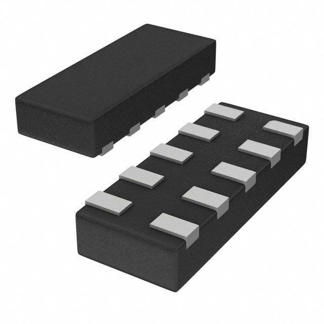
| 描述 | TVS DIODE 5.5VWM 4.1VC 10XSONTVS二极管阵列 ESD protect Ultra- High-Speed Interface |
| 产品分类 | |
| 品牌 | NXP Semiconductors |
| 产品手册 | |
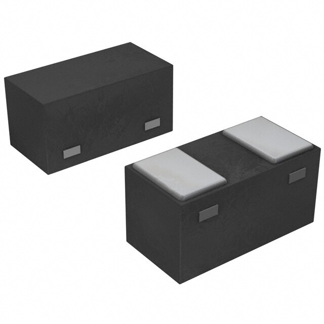
| 产品图片 |
|
| rohs | 符合RoHS无铅 / 符合限制有害物质指令(RoHS)规范要求 |
| 产品系列 | 二极管与整流器,TVS二极管,TVS二极管阵列,NXP Semiconductors IP4294CZ10-TBR,115- |
| mouser_ship_limit | 该产品可能需要其他文件才能进口到中国。 |
| 数据手册 | |
| 产品型号 | IP4294CZ10-TBR,115 |
| PCN封装 | |
| 不同频率时的电容 | - |
| 产品种类 | TVS二极管阵列 |
| 供应商器件封装 | 10-XSON(2.5x1) |
| 其它名称 | 568-10490-6 |
| 击穿电压 | 6 V |
| 功率-峰值脉冲 | - |
| 包装 | Digi-Reel® |
| 单向通道 | - |
| 双向通道 | 4 |
| 商标 | NXP Semiconductors |
| 外壳高度 | 0.5 mm |
| 安装类型 | * |
| 安装风格 | SMD/SMT |
| 封装 | Reel |
| 封装/外壳 | 10-XFDFN |
| 封装/箱体 | DFN2510A-10 |
| 尺寸 | 1 mm W x 2.5 mm L x 0.5 mm H |
| 工作温度 | -40°C ~ 85°C (TA) |
| 工作电压 | 5.5 V |
| 工厂包装数量 | 5000 |
| 应用 | 通用 |
| 最大工作温度 | + 85 C |
| 最小工作温度 | - 40 C |
| 标准包装 | 1 |
| 电压-击穿(最小值) | 6V |
| 电压-反向关态(典型值) | 5.5V |
| 电压-箝位(最大值)@Ipp | 4.1V |
| 电容 | 0.6 pF |
| 电流-峰值脉冲(10/1000µs) | 4A (8/20µs) |
| 电源线路保护 | 是 |
| 端接类型 | SMD/SMT |
| 类型 | 转向装置(轨至轨) |
| 通道 | 4 Channels |
| 钳位电压 | 4.1 V |


- 商务部:美国ITC正式对集成电路等产品启动337调查
- 曝三星4nm工艺存在良率问题 高通将骁龙8 Gen1或转产台积电
- 太阳诱电将投资9.5亿元在常州建新厂生产MLCC 预计2023年完工
- 英特尔发布欧洲新工厂建设计划 深化IDM 2.0 战略
- 台积电先进制程称霸业界 有大客户加持明年业绩稳了
- 达到5530亿美元!SIA预计今年全球半导体销售额将创下新高
- 英特尔拟将自动驾驶子公司Mobileye上市 估值或超500亿美元
- 三星加码芯片和SET,合并消费电子和移动部门,撤换高东真等 CEO
- 三星电子宣布重大人事变动 还合并消费电子和移动部门
- 海关总署:前11个月进口集成电路产品价值2.52万亿元 增长14.8%


PDF Datasheet 数据手册内容提取
Important notice Dear Customer, On 7 February 2017 the former NXP Standard Product business became a new company with the tradename Nexperia. Nexperia is an industry leading supplier of Discrete, Logic and PowerMOS semiconductors with its focus on the automotive, industrial, computing, consumer and wearable application markets In data sheets and application notes which still contain NXP or Philips Semiconductors references, use the references to Nexperia, as shown below. Instead of http://www.nxp.com, http://www.philips.com/ or http://www.semiconductors.philips.com/, use http://www.nexperia.com Instead of sales.addresses@www.nxp.com or sales.addresses@www.semiconductors.philips.com, use salesaddresses@nexperia.com (email) Replace the copyright notice at the bottom of each page or elsewhere in the document, depending on the version, as shown below: - © NXP N.V. (year). All rights reserved or © Koninklijke Philips Electronics N.V. (year). All rights reserved Should be replaced with: - © Nexperia B.V. (year). All rights reserved. If you have any questions related to the data sheet, please contact our nearest sales office via e-mail or telephone (details via salesaddresses@nexperia.com). Thank you for your cooperation and understanding, Kind regards, Team Nexperia
IP4294CZ10-TBR XSON10 ESD protection for ultra high-speed interfaces Rev. 4 — 1 November 2013 Product data sheet 1. Product profile 1.1 General description The device is designed to protect high-speed interfaces such as SuperSpeed USB, High-Definition Multimedia Interface(HDMI), DisplayPort, external Serial Advanced Technology Attachment(eSATA) and Low Voltage Differential Signaling(LVDS) interfaces against ElectroStatic Discharge(ESD). The device includes four high-level ESDprotection diode structures for ultra high-speed signal lines and is encapsulated in a leadless small DFN2510A-10(SOT1176-1) plastic package. All signal lines are protected by a special diode configuration offering ultra low line capacitance of only 0.5pF. These diodes utilize a unique snap-back structure in order to provide protection to downstream components from ESDvoltages up to 10kV contact exceeding IEC61000-4-2, level4. 1.2 Features and benefits System ESD protection for USB2.0 and SuperSpeed USB3.0, HDMI, DisplayPort, eSATA and LVDS All signal lines with integrated rail-to-rail clamping diodes for downstream ESDprotection of 10kV exceeding IEC61000-4-2, level4 Matched 0.5mm trace spacing Signal lines with 0.05pF matching capacitance between signal pairs Line capacitance of only 0.5pF for each channel Design-friendly ‘pass-through’ signal routing 1.3 Applications The device is designed for high-speed receiver and transmitter port protection: TVs and monitors DVD recorders and players Notebooks, main board graphic cards and ports Set-top boxes and game consoles
IP4294CZ10-TBR NXP Semiconductors ESD protection for ultra high-speed interfaces 2. Pinning information Table 1. Pinning Pin Symbol Description Simplified outline Graphic symbol 1 CH1 channel 1 ESDprotection 10 9 8 7 6 1 2 4 5 2 CH2 channel 2 ESDprotection 3 GND ground 4 CH3 channel 3 ESDprotection 1 2 3 4 5 5 CH4 channel 4 ESDprotection Transparent top view 6 n.c. not connected 3, 8 018aaa001 7 n.c. not connected 8 GND ground 9 n.c. not connected 10 n.c. not connected 3. Ordering information Table 2. Ordering information Type number Package Name Description Version IP4294CZ10-TBR DFN2510A-10 plastic extremely thin small outline package; SOT1176-1 noleads; 10terminals; body 12.50.5mm 4. Marking Table 3. Marking codes Type number Marking code IP4294CZ10-TBR 94 5. Limiting values Table 4. Limiting values In accordance with the Absolute Maximum Rating System (IEC 60134). Symbol Parameter Conditions Min Max Unit V input voltage 0.5 +5.5 V I V electrostatic discharge IEC61000-4-2, level4 [1] ESD voltage contactdischarge 10 +10 kV air discharge 15 +15 kV T ambient temperature 40 +85 C amb T storage temperature 55 +125 C stg [1] All pins to ground. IP4294CZ10-TBR All information provided in this document is subject to legal disclaimers. © NXP B.V. 2013. All rights reserved. Product data sheet Rev. 4 — 1 November 2013 2 of 12
IP4294CZ10-TBR NXP Semiconductors ESD protection for ultra high-speed interfaces 6. Characteristics Table 5. Characteristics T =25C unless otherwise specified. amb Symbol Parameter Conditions Min Typ Max Unit V breakdownvoltage I =1mA 6 - - V BR I I reverse leakage current per channel; V =3V - - 1 A LR I V forward voltage I =1mA - 0.7 - V F I C line capacitance f=1MHz; V =3.3V [1] - 0.5 0.6 pF line I C line capacitance f=1MHz; V =3.3V [1] - 0.05 - pF line I difference r dynamic resistance surge [2] dyn positive transient - 0.36 - negative transient - 0.35 - TLP [3] positive transient - 0.41 - negative transient - 0.34 - V clamping voltage I =4A [2] CL PP positive transient - 4.1 - V I =4A [2] PP negative transient - 2.2 - V [1] This parameter is guaranteed by design. [2] According to IEC61000-4-5 (8/20s current waveform). [3] 100ns Transmission Line Pulse(TLP); 50; pulser at 80ns. IP4294CZ10-TBR All information provided in this document is subject to legal disclaimers. © NXP B.V. 2013. All rights reserved. Product data sheet Rev. 4 — 1 November 2013 3 of 12
IP4294CZ10-TBR NXP Semiconductors ESD protection for ultra high-speed interfaces aaa-009367 aaa-009368 2 1.2 Sdd21 (dB) a -2 0.8 -6 0.4 -10 -14 0 106 107 108 109 1010 0 1 2 3 4 5 f (MHz) VI (V) differential mode C a = ---------------l--i--n--e------------ C lineV =0 V I Fig 1. Insertion loss; typical values Fig 2. Relative capacitance as a function of input voltage; typical values aaa-009369 aaa-009370 0 120 Zdif Sdd21 (Ω) (dB) 110 -20 (2) 100 -40 90 (1) -60 80 106 107 108 109 1010 40.0 40.5 41.0 41.5 42.0 f (MHz) t (ns) Sdd21 normalized to 100; tr=200ps; differential pair CH1+CH2 differentialpairsCH1/CH2versusCH3/CH4 (1) IP4294CZ10-TBR on reference board (2) Reference board without device under test (DUT) Fig 3. Crosstalk; typical values Fig 4. Differential Time Domain Reflectometer(TDR) plot; typical values IP4294CZ10-TBR All information provided in this document is subject to legal disclaimers. © NXP B.V. 2013. All rights reserved. Product data sheet Rev. 4 — 1 November 2013 4 of 12
IP4294CZ10-TBR NXP Semiconductors ESD protection for ultra high-speed interfaces 018aaa206 018aaa207 5 0 IPP IPP (A) (A) 4 -0.9 3 -1.8 2 -2.7 1 -3.6 0 -4.5 0 1 2 3 4 5 -2.5 -2.0 -1.5 -1.0 -0.5 0 VCL (V) VCL (V) IEC61000-4-5; tp=8/20s; positive pulse IEC61000-4-5; tp=8/20s; negative pulse Fig 5. Dynamic resistance with positive clamping; Fig 6. Dynamic resistance with negative clamping; typical values typical values aaa-009373 aaa-009374 14 0 I I (A) (A) 12 -2 10 -4 8 -6 6 -8 4 -10 2 -12 0 -14 0 4 8 12 -6 -4 -2 0 VCL (V) VCL (V) t =100ns; Transmission Line Pulse(TLP) t =100ns; Transmission Line Pulse(TLP) p p Fig 7. Dynamic resistance with positive clamping; Fig 8. Dynamic resistance with negative clamping; typical values typical values The device uses an advanced clamping structure showing a negative dynamic resistance. This snap-back behavior strongly reduces the clamping voltage to the system behind the ESD protection during an ESD event. Do not connect unlimited DC current sources to the data lines to avoid keeping the ESD protection device in snap-back state after exceeding breakdown voltage (due to an ESD pulse for instance). IP4294CZ10-TBR All information provided in this document is subject to legal disclaimers. © NXP B.V. 2013. All rights reserved. Product data sheet Rev. 4 — 1 November 2013 5 of 12
IP4294CZ10-TBR NXP Semiconductors ESD protection for ultra high-speed interfaces 7. Application information The device is designed to provide high-level ESDprotection for high-speed serial databuses such as HDMI, DisplayPort, eSATA and LVDS data lines. When designing the Printed-Circuit Board(PCB), give careful consideration to impedance matching and signal coupling. Do not connect the signal lines to unlimited current sources like, for example, a battery. A basic application diagram for the ESD protection of an HDMI interface is shown in Figure9. IP4294CZ10-TBR TMDS_D2+ TMDS_CH2+ 5 TMDS_GND TMDS_CH2– 4 TMDS_D2– GND 8 3 TMDS_D1+ TMDS_CH1+ 2 TMDS_GND TMDS_CH1– 1 TMDS_D1– IP4294CZ10-TBR TMDS_D0+ TMDS_CH2+ 5 TMDS_GND TMDS_CH2– 4 TMDS_D0– GND 8 3 TMDS_CLK+ HDMI TMDS_CH1+ CONNECTOR 2 TMDS_GND TMDS_CH1– 1 TMDS_CLK- CEC n.c. DDC_CLK DDC_DAT GND +5 V HOT PLUG DETECTION 6 5 4 IP4221CZ6 100 nF 1 2 3 018aaa174 Fig 9. Application diagram of HDMI ESD protection using IP4294CZ10-TBR IP4294CZ10-TBR All information provided in this document is subject to legal disclaimers. © NXP B.V. 2013. All rights reserved. Product data sheet Rev. 4 — 1 November 2013 6 of 12
IP4294CZ10-TBR NXP Semiconductors ESD protection for ultra high-speed interfaces 8. Package outline 1.1 0.9 0.127 0.2 min 5 6 2.6 0.25 2 2.4 0.15 0.5 1 10 0.4 0.45 0.3 0.05 max 0.35 0.5 max Dimensions in mm 12-05-23 Fig 10. Package outline DFN2510A-10(SOT1176-1) IP4294CZ10-TBR All information provided in this document is subject to legal disclaimers. © NXP B.V. 2013. All rights reserved. Product data sheet Rev. 4 — 1 November 2013 7 of 12
IP4294CZ10-TBR NXP Semiconductors ESD protection for ultra high-speed interfaces 9. Soldering Footprint information for reflow soldering of DFN2510A-10 package SOT1176-1 Hx C Hy Ay By 0.05 D P 0.05 Generic footprint pattern Refer to the package outline drawing for actual layout solder land solder paste deposit solder land plus solder paste occupied area solder resist Dimensions in mm Remark: P Ay By C D Hx Hy Stencil of 75 μm is recommended. A stencil of 75 μm gives an aspect ratio of 0.77 0.5 1.25 0.3 0.475 0.2 2.45 1.5 With a stencil of 100 μm one will obtain an aspect ratio of 0.58 sot1176-1_fr Fig 11. Reflow soldering footprint DFN2510A-10(SOT1176-1) IP4294CZ10-TBR All information provided in this document is subject to legal disclaimers. © NXP B.V. 2013. All rights reserved. Product data sheet Rev. 4 — 1 November 2013 8 of 12
IP4294CZ10-TBR NXP Semiconductors ESD protection for ultra high-speed interfaces 10. Revision history Table 6. Revision history Document ID Release date Data sheet status Change notice Supersedes IP4294CZ10-TBRv.4 20131101 Product data sheet - IP4294CZ10-TBRv.3 Modifications: • Measurements updated after silicon manufacturing transfer. IP4294CZ10-TBRv.3 20120224 Product data sheet - IP4294CZ10-TBRv.2 IP4294CZ10-TBRv.2 20120229 Preliminary data sheet - IP4294CZ10-TBRv.1 IP4294CZ10-TBRv.1 20111125 Preliminary data sheet - - IP4294CZ10-TBR All information provided in this document is subject to legal disclaimers. © NXP B.V. 2013. All rights reserved. Product data sheet Rev. 4 — 1 November 2013 9 of 12
IP4294CZ10-TBR NXP Semiconductors ESD protection for ultra high-speed interfaces 11. Legal information 11.1 Data sheet status Document status[1][2] Product status[3] Definition Objective [short] data sheet Development This document contains data from the objective specification for product development. Preliminary [short] data sheet Qualification This document contains data from the preliminary specification. Product [short] data sheet Production This document contains the product specification. [1] Please consult the most recently issued document before initiating or completing a design. [2] The term ‘short data sheet’ is explained in section “Definitions”. [3] The product status of device(s) described in this document may have changed since this document was published and may differ in case of multiple devices. The latest product status information is available on the Internet at URLhttp://www.nxp.com. 11.2 Definitions Suitability for use — NXP Semiconductors products are not designed, authorized or warranted to be suitable for use in life support, life-critical or safety-critical systems or equipment, nor in applications where failure or Draft — The document is a draft version only. The content is still under malfunction of an NXP Semiconductors product can reasonably be expected internal review and subject to formal approval, which may result in to result in personal injury, death or severe property or environmental modifications or additions. NXP Semiconductors does not give any damage. NXP Semiconductors and its suppliers accept no liability for representations or warranties as to the accuracy or completeness of inclusion and/or use of NXP Semiconductors products in such equipment or information included herein and shall have no liability for the consequences of applications and therefore such inclusion and/or use is at the customer’s own use of such information. risk. Short data sheet — A short data sheet is an extract from a full data sheet Applications — Applications that are described herein for any of these with the same product type number(s) and title. A short data sheet is intended products are for illustrative purposes only. NXP Semiconductors makes no for quick reference only and should not be relied upon to contain detailed and representation or warranty that such applications will be suitable for the full information. For detailed and full information see the relevant full data specified use without further testing or modification. sheet, which is available on request via the local NXP Semiconductors sales office. In case of any inconsistency or conflict with the short data sheet, the Customers are responsible for the design and operation of their applications full data sheet shall prevail. and products using NXP Semiconductors products, and NXP Semiconductors accepts no liability for any assistance with applications or customer product Product specification — The information and data provided in a Product design. It is customer’s sole responsibility to determine whether the NXP data sheet shall define the specification of the product as agreed between Semiconductors product is suitable and fit for the customer’s applications and NXP Semiconductors and its customer, unless NXP Semiconductors and products planned, as well as for the planned application and use of customer have explicitly agreed otherwise in writing. In no event however, customer’s third party customer(s). Customers should provide appropriate shall an agreement be valid in which the NXP Semiconductors product is design and operating safeguards to minimize the risks associated with their deemed to offer functions and qualities beyond those described in the applications and products. Product data sheet. NXP Semiconductors does not accept any liability related to any default, damage, costs or problem which is based on any weakness or default in the 11.3 Disclaimers customer’s applications or products, or the application or use by customer’s third party customer(s). Customer is responsible for doing all necessary testing for the customer’s applications and products using NXP Limited warranty and liability — Information in this document is believed to Semiconductors products in order to avoid a default of the applications and be accurate and reliable. However, NXP Semiconductors does not give any the products or of the application or use by customer’s third party representations or warranties, expressed or implied, as to the accuracy or customer(s). NXP does not accept any liability in this respect. completeness of such information and shall have no liability for the consequences of use of such information. NXP Semiconductors takes no Limiting values — Stress above one or more limiting values (as defined in responsibility for the content in this document if provided by an information the Absolute Maximum Ratings System of IEC60134) will cause permanent source outside of NXP Semiconductors. damage to the device. Limiting values are stress ratings only and (proper) operation of the device at these or any other conditions above those given in In no event shall NXP Semiconductors be liable for any indirect, incidental, the Recommended operating conditions section (if present) or the punitive, special or consequential damages (including - without limitation - lost Characteristics sections of this document is not warranted. Constant or profits, lost savings, business interruption, costs related to the removal or repeated exposure to limiting values will permanently and irreversibly affect replacement of any products or rework charges) whether or not such the quality and reliability of the device. damages are based on tort (including negligence), warranty, breach of contract or any other legal theory. Terms and conditions of commercial sale — NXP Semiconductors products are sold subject to the general terms and conditions of commercial Notwithstanding any damages that customer might incur for any reason whatsoever, NXP Semiconductors’ aggregate and cumulative liability towards sale, as published at http://www.nxp.com/profile/terms, unless otherwise customer for the products described herein shall be limited in accordance agreed in a valid written individual agreement. In case an individual with the Terms and conditions of commercial sale of NXP Semiconductors. agreement is concluded only the terms and conditions of the respective agreement shall apply. NXP Semiconductors hereby expressly objects to Right to make changes — NXP Semiconductors reserves the right to make applying the customer’s general terms and conditions with regard to the changes to information published in this document, including without purchase of NXP Semiconductors products by customer. limitation specifications and product descriptions, at any time and without notice. This document supersedes and replaces all information supplied prior No offer to sell or license — Nothing in this document may be interpreted or to the publication hereof. construed as an offer to sell products that is open for acceptance or the grant, conveyance or implication of any license under any copyrights, patents or other industrial or intellectual property rights. IP4294CZ10-TBR All information provided in this document is subject to legal disclaimers. © NXP B.V. 2013. All rights reserved. Product data sheet Rev. 4 — 1 November 2013 10 of 12
IP4294CZ10-TBR NXP Semiconductors ESD protection for ultra high-speed interfaces Export control — This document as well as the item(s) described herein product for such automotive applications, use and specifications, and (b) may be subject to export control regulations. Export might require a prior whenever customer uses the product for automotive applications beyond authorization from competent authorities. NXP Semiconductors’ specifications such use shall be solely at customer’s own risk, and (c) customer fully indemnifies NXP Semiconductors for any Quick reference data — The Quick reference data is an extract of the liability, damages or failed product claims resulting from customer design and product data given in the Limiting values and Characteristics sections of this use of the product for automotive applications beyond NXP Semiconductors’ document, and as such is not complete, exhaustive or legally binding. standard warranty and NXP Semiconductors’ product specifications. Non-automotive qualified products — Unless this data sheet expressly Translations — A non-English (translated) version of a document is for states that this specific NXP Semiconductors product is automotive qualified, reference only. The English version shall prevail in case of any discrepancy the product is not suitable for automotive use. It is neither qualified nor tested between the translated and English versions. in accordance with automotive testing or application requirements. NXP Semiconductors accepts no liability for inclusion and/or use of non-automotive qualified products in automotive equipment or applications. 11.4 Trademarks In the event that customer uses the product for design-in and use in automotive applications to automotive specifications and standards, customer Notice: All referenced brands, product names, service names and trademarks (a) shall use the product without NXP Semiconductors’ warranty of the are the property of their respective owners. 12. Contact information For more information, please visit: http://www.nxp.com For sales office addresses, please send an email to: salesaddresses@nxp.com IP4294CZ10-TBR All information provided in this document is subject to legal disclaimers. © NXP B.V. 2013. All rights reserved. Product data sheet Rev. 4 — 1 November 2013 11 of 12
IP4294CZ10-TBR NXP Semiconductors ESD protection for ultra high-speed interfaces 13. Contents 1 Product profile. . . . . . . . . . . . . . . . . . . . . . . . . . 1 1.1 General description . . . . . . . . . . . . . . . . . . . . . 1 1.2 Features and benefits. . . . . . . . . . . . . . . . . . . . 1 1.3 Applications . . . . . . . . . . . . . . . . . . . . . . . . . . . 1 2 Pinning information. . . . . . . . . . . . . . . . . . . . . . 2 3 Ordering information. . . . . . . . . . . . . . . . . . . . . 2 4 Marking. . . . . . . . . . . . . . . . . . . . . . . . . . . . . . . . 2 5 Limiting values. . . . . . . . . . . . . . . . . . . . . . . . . . 2 6 Characteristics. . . . . . . . . . . . . . . . . . . . . . . . . . 3 7 Application information. . . . . . . . . . . . . . . . . . . 6 8 Package outline. . . . . . . . . . . . . . . . . . . . . . . . . 7 9 Soldering . . . . . . . . . . . . . . . . . . . . . . . . . . . . . . 8 10 Revision history. . . . . . . . . . . . . . . . . . . . . . . . . 9 11 Legal information. . . . . . . . . . . . . . . . . . . . . . . 10 11.1 Data sheet status . . . . . . . . . . . . . . . . . . . . . . 10 11.2 Definitions. . . . . . . . . . . . . . . . . . . . . . . . . . . . 10 11.3 Disclaimers. . . . . . . . . . . . . . . . . . . . . . . . . . . 10 11.4 Trademarks. . . . . . . . . . . . . . . . . . . . . . . . . . . 11 12 Contact information. . . . . . . . . . . . . . . . . . . . . 11 13 Contents. . . . . . . . . . . . . . . . . . . . . . . . . . . . . . 12 Please be aware that important notices concerning this document and the product(s) described herein, have been included in section ‘Legal information’. © NXP B.V. 2013. All rights reserved. For more information, please visit: http://www.nxp.com For sales office addresses, please send an email to: salesaddresses@nxp.com Date of release: 1 November 2013 Document identifier: IP4294CZ10-TBR