 Datasheet下载
- 型号: SMF12AT1G
- 制造商: ON Semiconductor
- 库位|库存: xxxx|xxxx
- 要求:
| 数量阶梯 | 香港交货 | 国内含税 |
| +xxxx | $xxxx | ¥xxxx |
查看当月历史价格
查看今年历史价格
SMF12AT1G产品简介:
ICGOO电子元器件商城为您提供SMF12AT1G由ON Semiconductor设计生产,在icgoo商城现货销售,并且可以通过原厂、代理商等渠道进行代购。 SMF12AT1G价格参考¥0.76-¥0.76。ON SemiconductorSMF12AT1G封装/规格:TVS - 二极管, 。您可以下载SMF12AT1G参考资料、Datasheet数据手册功能说明书,资料中有SMF12AT1G 详细功能的应用电路图电压和使用方法及教程。
Littelfuse Inc.的SMF12AT1G是一款瞬态电压抑制(TVS)二极管,广泛应用于各种电子设备中,用于保护电路免受瞬时电压尖峰的损害。这类二极管的特点是能够在极短时间内响应并吸收大量的瞬态能量,从而保护敏感的电子元件不受损坏。

 应用场景:

1. 消费电子产品:
   - 智能手机和平板电脑:SMF12AT1G可用于保护USB接口、充电接口、耳机插孔等易受静电放电(ESD)和瞬态电压影响的部分。
   - 笔记本电脑和台式机:保护电源输入端口、网络接口和其他外设接口免受电压波动的影响。

2. 通信设备:
   - 路由器和调制解调器:用于保护以太网端口、Wi-Fi模块和其他通信接口,防止雷击或电力波动引起的瞬态电压损坏设备。
   - 无线通信模块:保护天线接口和射频前端电路,确保信号传输的稳定性和可靠性。

3. 汽车电子系统:
   - 车载娱乐系统:保护音频和视频输入输出接口,防止车辆启动时的电压波动或其他电气干扰。
   - 传感器和控制系统:保护传感器信号线和控制单元,确保数据传输的准确性和系统的稳定性。

4. 工业自动化设备:
   - 可编程逻辑控制器(PLC):保护输入输出模块,确保在恶劣的工业环境中正常工作。
   - 传感器和执行器:保护信号线和电源线,防止外部电磁干扰和电压瞬变。

5. 医疗设备:
   - 便携式医疗设备:如血糖仪、血压计等,保护其接口和内部电路,确保测量结果的准确性。
   - 大型医疗设备:如X光机、超声波设备等,保护其复杂的电子控制系统,确保设备的安全性和可靠性。

6. 家用电器:
   - 智能家电:如智能冰箱、洗衣机等,保护其联网模块和控制面板,防止外界干扰导致的故障。

总之,SMF12AT1G TVS二极管通过其快速响应特性和强大的瞬态能量吸收能力,为各种电子设备提供了可靠的保护,确保这些设备在复杂多变的电气环境中能够稳定运行。
| 参数 | 数值 |
| 产品目录 | |
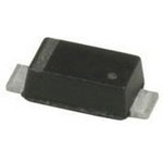
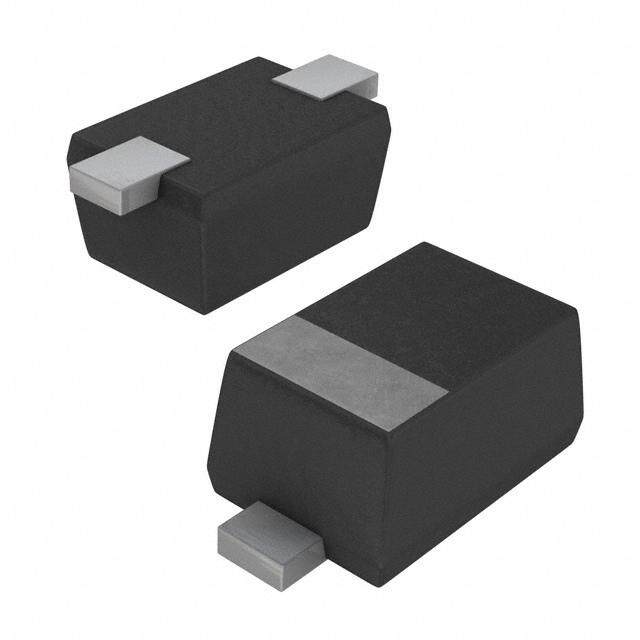
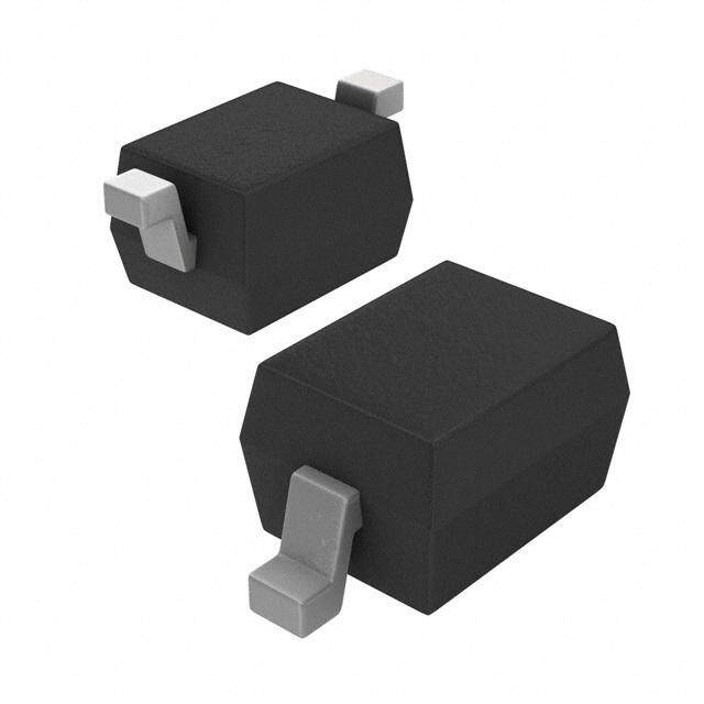
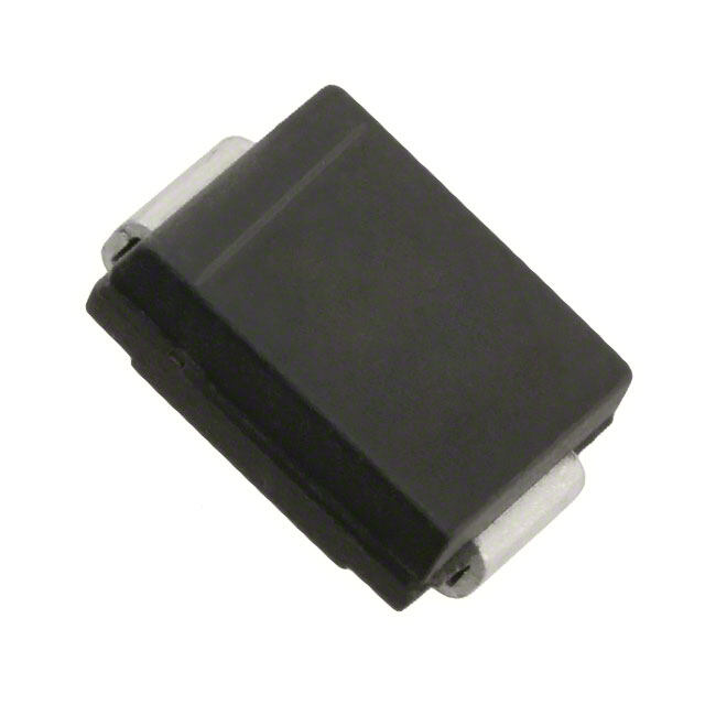
| 描述 | TVS DIODE 12VWM 19.9VC SOD123FL |
| 产品分类 | |
| 品牌 | ON Semiconductor |
| 数据手册 | |
| 产品图片 |
|
| 产品型号 | SMF12AT1G |
| PCN设计/规格 | |
| rohs | 无铅 / 符合限制有害物质指令(RoHS)规范要求 |
| 产品系列 | - |
| 不同频率时的电容 | - |
| 供应商器件封装 | SOD-123FL |
| 其它名称 | SMF12AT1GOSCT |
| 功率-峰值脉冲 | 1000W (1kW) |
| 包装 | 剪切带 (CT) |
| 单向通道 | 1 |
| 双向通道 | - |
| 安装类型 | 表面贴装 |
| 封装/外壳 | SOD-123F |
| 工作温度 | -55°C ~ 150°C |
| 应用 | 通用 |
| 标准包装 | 1 |
| 电压-击穿(最小值) | 13.3V |
| 电压-反向关态(典型值) | 12V |
| 电压-箝位(最大值)@Ipp | 19.9V |
| 电流-峰值脉冲(10/1000µs) | 10.1A (8/20µs) |
| 电源线路保护 | 无 |
| 类型 | 齐纳 |


- 商务部:美国ITC正式对集成电路等产品启动337调查
- 曝三星4nm工艺存在良率问题 高通将骁龙8 Gen1或转产台积电
- 太阳诱电将投资9.5亿元在常州建新厂生产MLCC 预计2023年完工
- 英特尔发布欧洲新工厂建设计划 深化IDM 2.0 战略
- 台积电先进制程称霸业界 有大客户加持明年业绩稳了
- 达到5530亿美元!SIA预计今年全球半导体销售额将创下新高
- 英特尔拟将自动驾驶子公司Mobileye上市 估值或超500亿美元
- 三星加码芯片和SET,合并消费电子和移动部门,撤换高东真等 CEO
- 三星电子宣布重大人事变动 还合并消费电子和移动部门
- 海关总署:前11个月进口集成电路产品价值2.52万亿元 增长14.8%


PDF Datasheet 数据手册内容提取
TVS Diodes Surface Mount > 200W > SMF5.0AT1G Series SMF5.0AT1G Series Pb Description The SMF5.0AT1G Series is designed to protect voltage sensitive components from high voltage, high energy transients. Excellent clamping capability, high surge capability, low zener impedance and fast response time. Because of its small size, it is ideal for use in cellular phones, portable devices, business machines, power supplies and many other industrial/consumer applications. Features • Stand−off Voltage: 5 − 58 Volts • Peak Power − 200 Watts @ 1 ms (SMF5.0A − SMF58A) • Low Leakage Maximum Ratings and Thermal Characteristics • Response Time is Typically < 1 ns Rating Symbol Value Unit • ESD Rating of Class 3 (> 16 kV) per Human Body Model • ESD Rating of Level 4 (8 kV Contact Discharge) per Maximum Ppk Dissipation (PW−10/1000 P 200 W µs) (Note 1) SMF5.0A − SMF58A PK IEC61000−4−2 • EFT (Electrical Fast Transients) Rating of 40 A per Maximum Ppk Dissipation @ TA = 25°C, P 1000 W (PW−8/20 µs) (Note 2) PK IEC61000−4−4 • Low Profile − Maximum Height of 1.0 mm D(NCo tPeo 3w)er Dissipation @ TA = 25°C PD 385 mW • Small Footprint − Footprint Area of 8.45 mm2 Derate Above 25°C 4.0 mW/°C Thermal Resistance from Junction−to− R8JA 325 °C/W • Supplied in 8 mm Tape and Reel − 3,000 Units per Reel Ambient (Note 3) • Cathode Indicated by Polarity Band Operating and Storage Temperature −55 to Range TJ, Tstg +150 °C • Lead Orientation in TaBpie-:d Ciraetchtoiodnea Lle ad to Sprocket Holes • These Devices are Pb−Free and are RoHS Compliant Stresses exceeding Maximum Ratings may damage the device. Maximum Ratings are stress ratings only. Functional operation above the Recommended Operating Conditions is not implied. Extended exposure to stresses above the Recommended Operating Conditions Functional Diagram may affect device reliability. 1. Non−repetitive current pulse at TA = 25°C, per waveform of Figure 2. 2. Non−repetitive current pulse at TA = 25°C, per waveform of Figure 3. 3. Mounted with recommended minimum pad size, DC board FR−4. Cathode Anode Additional Information Uni-directional Datasheet Resources Samples © 2017 Littelfuse, Inc. Specifications are subject to change without notice. Revised: 09/13/17
TVS Diodes Surface Mount > 200W > SMF5.0AT1G Series I-V Curve Characteristics (T = 25°C unless otherwise noted, V = 3.5 V Max. @ I (Note 4) = 12 A) A F F Symbol Parameter I I I Maximum Reverse Peak Pulse Current PP V Clamping Voltage @ I C PP V Working Peak Reverse Voltage RWM I Maximum Reverse Leakage Current @ V R RWM I V I V Breakdown Voltage @ I BR T I Test Current T I Forward Current F I V Forward Voltage @ I F F 4. 1/2 sine wave (or equivalent square wave), PW = 8.3 ms, duty cycle = 4 pulses per minute maximum. Ratings and Characteristic Curves Figure 1. Pulse Rating Curve Figure 2. 10 X 1000 µs Pulse Waveform 10,000 tr . 100 1000 I tʺ 10 s I 2 100 tP 10 0 1.01 0 100 1000 10,000 t Figure 3. 8 X 20 µs Pulse Waveform Figure 4. Pulse Derating Curve 100 tr PEAK VALUE IRSM @ 8 s °160 PULSE WIDTH (tP) IS DEFINED AS THAT POINT WHERE THE 120 PEAK CURRENT DECAY = 8 s 60 100 HALF VALUE IRSM/2 @ 20 s 60 tP 20 10 20 0 0 ° © 2017 Littelfuse, Inc. Specifications are subject to change without notice. Revised: 09/13/17
TVS Diodes Surface Mount > 200W > SMF5.0AT1G Series Figure 5. Typical Derating Factor for Duty Cycle Figure 6. Steady State Power Derating 1 0.2 0.1 200 100 0.02 100 s 10 s 0.01 0 1 20 100 0 ° Figure 7. Forward Voltage Figure 8. Capacitance vs. Working Peak Reverse Voltage 1000 1.2 1.0 100 0.6 10 0.2 0 1 1 10 100 1000 ° © 2017 Littelfuse, Inc. Specifications are subject to change without notice. Revised: 09/13/17
TVS Diodes Surface Mount > 200W > SMF5.0AT1G Series Electrical Characteristics (T = 30°C unless otherwise noted, V = 1.25 Volts @ 200 mA) L F I (Max) V I @ V V @ I (V) (Note 6) @ I I @ V V (Max) PP Device RWM R RWM BR T T R RWM C (A) Device Marking V μA Min Nom Max mA (µA) (V) (Note 7) SMF5.0AG KE 5 400 6.4 6.7 7.0 10 400 9.2 21.7 SMF6.0AG KG 6 400 6.67 7.02 7.37 10 400 10.3 19.4 SMF6.5AG KK 6.5 250 7.22 7.60 7.98 10 250 11.2 17.9 SMF7.0AG KM 7 100 7.78 8.19 8.6 10 100 12 16.7 SMF7.5AG KP 7.5 50 8.33 8.77 9.21 1 50 12.9 15.5 SMF8.0AG KR 8 25 8.89 9.36 9.83 1 25 13.6 14.7 SMF9.0AG KV 9 5 10 10.55 11.1 1 5 15.4 13.0 SMF10AG KX 10 2.5 11.1 11.7 12.3 1 2.5 17 11.8 SMF11AG KZ 11 2.5 12.2 12.85 13.5 1 2.5 18.2 11.0 SMF12AG LE 12 2.5 13.3 14 14.7 1 2.5 19.9 10.1 SMF13AG LG 13 1 14.4 15.15 15.9 1 1 21.5 9.3 SMF14AG LK 14 1 15.6 16.4 17.2 1 1 23.2 8.6 SMF15AG LM 15 1 16.7 17.6 18.5 1 1 24.4 8.2 SMF18AG LT 18 1 20 21 22.1 1 1 29.2 6.8 SMF20AG LV 20 1 22.2 23.35 24.5 1 1 32.4 6.2 SMF22AG LX 22 1 24.4 25.6 26.9 1 1 35.5 5.6 SMF24AG LZ 24 1 26.7 28.1 29.5 1 1 38.9 5.1 SMF26AG ME 26 1 28.9 30.4 31.9 1 1 42.1 4.8 SMF28AG MG 28 1 31.1 32.8 34.4 1 1 45.4 4.4 SMF30AG MK 30 1 33.3 35.1 36.8 1 1 48.4 4.1 SMF33AG MM 33 1 36.7 38.7 40.6 1 1 53.3 3.8 SMF36AG MP 36 1 40 42.1 44.2 1 1 58.1 3.4 SMF48AG MX 48 1 53.3 56.1 58.9 1 1 77.4 2.6 SMF51AG MZ 51 1 56.7 59.7 62.7 1 1 82.4 2.4 SMF58AG NG 58 1 64.4 67.8 71.2 1 1 93.6 2.1 5. A transient suppressor is normally selected according to the Working Peak Reverse Voltage (V ) which RWM should be equal to or greater than the DC or continuous peak operating voltage level. 6. V measured at pulse test current I at ambient temperature of 25°C. BR T 7. Surge current waveform per Figure 2 and derate per Figure 3. © 2017 Littelfuse, Inc. Specifications are subject to change without notice. Revised: 09/13/17
TVS Diodes Surface Mount > 200W > SMF5.0AT1G Series Dimensions Soldering Footrpint E D 1 2 A1 POOPLTAIORNITAYL IANSD INCEAETDOERD A TOP VIEW END VIEW HE c ORDERING INFORMATION SIDE VIEW 2XL Device Package Shipping† 2Xb SOD−123FL 3,000 / SMFxxxAT1G (Pb−Free) Tape & Reel BOTTOM VIEW Inches Millimeters Flow/Wave Soldering (Solder Dipping) Dim Min Nom Max Min Nom Max 260ºC A 0.035 0.037 0.039 0.90 0.95 0.98 Peak Temperature : Device Meets MSL 1 A1 0.000 0.002 0.004 0.00 0.05 0.10 Requirements b 0.028 0.035 0.043 0.70 0.90 1.10 c 0.004 0.006 0.008 0.10 0.15 0.20 Physical Specifications D 0.059 0.065 0.071 1.50 1.65 1.80 E 0.098 0.106 0.114 2.50 2.70 2.90 Case Void-free, transfer-molded, thermosetting plastic Epoxy Meets UL 94 V−0 L 0.022 0.030 0.037 0.55 0.75 0.95 HE 0.134 0.142 0.150 3.40 3.60 3.80 Lead Finish 100% Matte Sn (Tin) 0 0° − 8° 0° − 8° NOTES: Mounting Position Any 1. DIMENSIONING AND TOLERANCING PER ANSI Y14.5M, 1982. 2. CONTROLLING DIMENSION: MILLIMETER. 3. DIMENSIONS A AND B DO NOT INCLUDE MOLD FLASH. 4. DIMENSIONS D AND J ARE TO BE MEASURED ON FLAT SECTION OF THE LEAD: BETWEEN 0.10 AND 0.25 MM FROM THE LEAD TIP. Part Marking System 1 2 Disclaimer Notice - Information furnished is believed to be accurate and reliable. However, users should independently evaluate the suitability of and test each product selected for their own applications. Littelfuse products are not designed for, and may not be used in, all applications. Read complete Disclaimer Notice at: www.littelfuse.com/disclaimer-electronics. © 2017 Littelfuse, Inc. Specifications are subject to change without notice. Revised: 09/13/17