ICGOO在线商城 > GP2A25J0000F
 Datasheet下载
- 型号: GP2A25J0000F
- 制造商: Sharp Microelectronics
- 库位|库存: xxxx|xxxx
- 要求:
| 数量阶梯 | 香港交货 | 国内含税 |
| +xxxx | $xxxx | ¥xxxx |
查看当月历史价格
查看今年历史价格
GP2A25J0000F产品简介:
ICGOO电子元器件商城为您提供GP2A25J0000F由Sharp Microelectronics设计生产,在icgoo商城现货销售,并且可以通过原厂、代理商等渠道进行代购。 提供GP2A25J0000F价格参考以及Sharp MicroelectronicsGP2A25J0000F封装/规格参数等产品信息。 你可以下载GP2A25J0000F参考资料、Datasheet数据手册功能说明书, 资料中有GP2A25J0000F详细功能的应用电路图电压和使用方法及教程。
| 参数 | 数值 |
| 产品目录 | |
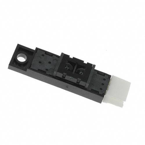
| 描述 | SENSR OPTO REFL 1MM-9MM CON HORZ光学开关(反射型,光电IC输出) OPIC Photointerpter 3-7mm lgth rnd lens |
| 产品分类 | |
| 品牌 | Sharp Microelectronics |
| 产品手册 | |
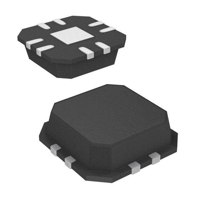
| 产品图片 |
|
| rohs | 符合RoHS无铅 / 符合限制有害物质指令(RoHS)规范要求 |
| 产品系列 | 光学开关(反射型,光电IC输出),Sharp Microelectronics GP2A25J0000F- |
| 数据手册 | http://www.sharpsma.com/webfm_send/1273 |
| 产品型号 | GP2A25J0000F |
| PCN设计/规格 | http://www.sharpsma.com/webfm_send/1525 |
| 产品目录页面 | |
| 产品种类 | 光学开关(反射型,光电IC输出) |
| 低电平输出电压 | 0.4 V |
| 低电平输出电流 | 16 mA |
| 其它名称 | 425-2044-5 |
| 包装 | 散装 |
| 商标 | Sharp Microelectronics |
| 安装类型 | 底座安装 |
| 安装风格 | Snap In |
| 封装/外壳 | 模块,连接器 |
| 工厂包装数量 | 100 |
| 感应方式 | Reflective |
| 感应方法 | 反射 |
| 感应物体 | 黑色纸,Kodak® 灰色卡,白色纸 |
| 感应距离 | 0.039" ~ 0.354"(1mm ~ 9mm)ADJ |
| 感测光 | 红外线 |
| 最大工作温度 | + 60 C |
| 最小工作温度 | - 10 C |
| 标准包装 | 100 |
| 正向电流 | 30 mA |
| 波长 | 950 nm |
| 特性 | 长焦距 |
| 电压-电源 | 4.75 V ~ 5.25 V |
| 电流-电源 | - |
| 输出设备 | Totem Pole, Inverter |
| 输出配置 | - |
| 高电平输入电压 | 4.5 V |
| 高电平输出电流 | 50 mA |


- 商务部:美国ITC正式对集成电路等产品启动337调查
- 曝三星4nm工艺存在良率问题 高通将骁龙8 Gen1或转产台积电
- 太阳诱电将投资9.5亿元在常州建新厂生产MLCC 预计2023年完工
- 英特尔发布欧洲新工厂建设计划 深化IDM 2.0 战略
- 台积电先进制程称霸业界 有大客户加持明年业绩稳了
- 达到5530亿美元!SIA预计今年全球半导体销售额将创下新高
- 英特尔拟将自动驾驶子公司Mobileye上市 估值或超500亿美元
- 三星加码芯片和SET,合并消费电子和移动部门,撤换高东真等 CEO
- 三星电子宣布重大人事变动 还合并消费电子和移动部门
- 海关总署:前11个月进口集成电路产品价值2.52万亿元 增长14.8%


(SN).jpg)


PDF Datasheet 数据手册内容提取
GP2A25J0000F Series GP2A25J0000F Detecting Distance : 1 to 9mm *OPIC Output, Series Refl ective Photointerrupter with Connector ■Description ■Agency approvals/Compliance GP2A25J0000F Series are OPIC output, reflective 1. Compliant with RoHS directive photointerrupters with emitter and detector facing the same direction in a molding that provides non-contact ■Applications sensing. This family of devices uses light modulation to 1. General purpose detection of paper presence or mo- reduce the affects of disturbing light, and the sensor is tion. optimized to work in the selected focal distance. A 3-pin 2. Example : PPC, FAX, Printer connector is included to allow remote-mount or off-board designs. ■Features 1. Refl ective with OPIC Light Modulated Output 2. Highlights : • Includes additional screw fi xing holes • Position pin to prevent mis-alignment • Short focal distance 3. Key Parameters: • Detecting distance : 1 to 9mm (White paper) 3 to 7mm (Black paper) • Undetecting distance : over 27mm (White paper) • Connector : GP2A25J0000F ; Tyco Electronics AMP K.K. (PN : 292133-3) GP2A25DJ000F ; Tyco Electronics AMP K.K. (PN : 292133-3) GP2A25NJJ00F ; Tyco Electronics AMP K.K. (PN : 4-292133-3) 4. RoHS directive compliant * "OPIC"(Optical IC) is a trademark of the SHARP Corporation. An OPIC consists of a light-detecting element and a signal- processing Notice The content of data sheet is subject to change without prior notice. In the absence of confi rmation by device specifi cation sheets, SHARP takes no responsibility for any defects that may occur in equipment using any SHARP devices shown in catalogs, data books, etc. Contact SHARP in order to obtain the latest device specifi cation sheets before using any SHARP device. Sheet No.: D3-A04901FEN 1 Date Jun. 30. 2005 © SHARP Corporation
GP2A25J0000F Series ■Internal Connection Diagram Reflective object Demodulator circuit 1 Voltage regulator 1 VCC 2 2 VOUT 3 GND Amp. 3 Comparator Oscillator circuit Sync. detecting circuit ■Outline Dimensions (Unit : mm) GP2A25J0000F GP2A25DJ000F 33 26.5 3.1 17.7 Optical center φ3+−00.2 2 9 4.5 12 VVOCCUT 9.67 3.5 6.1 12 VVOCCUT 3 GND 3 GND φ3.2 6.2 6 φ3.2 Connector : 292133-3 (Tyco Electronics AMP K.K.) 12 12 Connector : 292133-3 (Tyco Electronics AMP K.K.) 7.8 7.5 6 Optical center 3 8 4.5 98 4.5 7.8 4.5 2.5 26.5 φ3+−00.2 1 2 3 2 φ3.2 7.9 4.3 φ3+−00.2 21 3.5 2 26.5 • Unspecifi ed tolerance 34.3 • Unspecifi ed tolerance shall be as follows ; shall be as follows ; 4-SR2 0 7 Dimensions Tolerance Dimensions Tolerance less than 6 ±0.2 9 6 less than 6 ±0.2 Date code 6 or more less 6 or more less ±0.3 ±0.3 than 14 than 14 Date code Product mass : approx. 1.95g 14 or more ±0.4 Product mass : approx. 2.4g 14 or more ±0.4 GP2A25NJJ00F Optical center 33 (6.8) 3.1 17.7 9 4.5 7.8) 12 VVOCCUT ( 3 GND φ3.2 6.2 6 12 Connector : 4-292133-3 7.8 (Tyco Electronics AMP K.K.) 8 4.5 (5 .8) 5 2. 26.5 φ3+−00.2 1 2 3 2 0 7 • Unspecifi ed tolerance shall be as follows ; Dimensions Tolerance Date code • ( ) : Reference dimensions. less than 6 ±0.2 • : Portion Built-in IR-90 fi lter 6 or more less ±0.3 than 14 Connector terminal plating material : Sn Product mass : approx. 1.95g 14 or more ±0.4 Sheet No.: D3-A04901FEN 2
GP2A25J0000F Series Date code (2 digit) 1st digit 2nd digit Year of production Month of production A.D. Mark Month Mark 2000 0 1 1 2001 1 2 2 2002 2 3 3 2003 3 4 4 2004 4 5 5 2005 5 6 6 2006 6 7 7 2007 7 8 8 2008 8 9 9 2009 9 10 X 2010 0 11 Y : : 12 Z repeats in a 10 year cycle Country of origin Japan Sheet No.: D3-A04901FEN 3
GP2A25J0000F Series ■Absolute Maximum Ratings (Ta=25˚C) Parameter Symbol Rating Unit Supply voltage VCC −0.5 to +7 V Output voltage V 30 V O *1 Output current I 50 mA OL *2 Operating temperature Topr −10 to +60 ˚C *2 Storage temperature Tstg −20 to +80 ˚C ∗1 Sink current refer to Fig.5. ∗2 The connector should be plugged in/out at normal temperature. ■Electro-optical Characteristics (Ta=25˚C) Parameter Symbol Condhitions MIN. TYP. MAX. Unit Supply voltage VCC − 4.75 − 5.25 V Current dissipation (I) ICC Smoothing value VCC=5V, RL=∞ − − 30 mA *3 Current dissipation (II) ICCP Pulse peak value VCC=5V − − 150 mA Low level output voltage VOL VCC=5V, IOL=16mA, at detecting time − − 0.4 V High level output voltage VOH VCC=5V, RL=1kΩ, at non detecting time 4.5 − − V *4 Non detection distance LLHL KODAK Gray Cards, VCC=5V − − 27 mm L KODAK Gray Cards, VCC=5V − − 1 mm *4 Detection distance HLS Black paper, VCC=5V − − 3 L KODAK Gray Cards, VCC=5V 9 − − mm HLL Black paper, VCC=5V 7 − − *5 Response time ttPPLHHL VCC=5V −− −− 11 mmss Ev1 3 000 − − lx *6 Acceptable illuminance − Ev2 1 500 − − lx ∗3 Refer to Fig.1. ∗4 Refer to Fig.2. ∗5 Refer to Fig.3. *6 Refer to Fig.4. Refl ective object Black paper (black) : Standard refl ective object (provided by SHARP Corporation) KODAK Gray Cards (use the white side refl ects about 90%) : Standard refl ective object (provided by SHARP Corporation) PPC paper : Standard refl ective object (provided by SHARP Corporation) Sheet No.: D3-A04901FEN 4
GP2A25J0000F Series Fig.1 Test Condition for Peak Pulse Value I CCP R=1Ω VCC=5V Vr 1 V RL=1kΩ 2 VO tW tP ItCP(CTP=YVP.r/)1=Ω130μs 3 GND tW(TYP.)=8μs Photointerrupter Fig.2 Test Condition for Detecting Distance Characteristics Reflective object VO VOH ut p ut O V OL Detecting distance L L L HLS HLL Detection surface L L LHS LHL Fig.3 Test Circuit for Response Time Reflective object With reflective object Detection surface RL=1kΩ 1 VCC=5V Without reflective object 2 VO tPHL tPLH V 3 GND OH V out 1.5V waveform V OL L Photointerrupter Fig.4 Test Condition for External Disturbing Light Illuminance PPC paper EV1 : At non-detecting EV2 : At detecting Emission/detection surface Emission/detection surface Light source A Light source A Photointerrupter Photointerrupter Illuminance shall be that on the reflective object. Output shall not go from "L" to "H". Illuminance shall be that on the emission/detection surface. 7mm Output shall not go from "H" to "L". Sheet No.: D3-A04901FEN 5
GP2A25J0000F Series Fig.5 Low Level Output Current vs. Fig.6 Low Level Output Voltage vs. Ambient Temperature Ambient Temperature 60 0.3 V =5V CC At detecting A) 50 V) (mL (OL IOL=30mA nt IO 40 ge V 0.2 e a urr olt ut c 30 ut v 16mA utp 27 utp o o vel 20 vel 0.1 e e w l w l o o 5mA L 10 L 0 0 −10 0 25 50 60 75 −10 0 25 50 75 Ambient temperature Ta (˚C) Ambient temperature Ta (˚C) Fig.7 Low Level Output Voltage vs. Fig.8 Dissipation Current(Smoothing Value) Low Level Output Current vs. Ambient Temperature 7 VCC=5V At detecting 6 V) e V (OL (mA)C 5 Ta=−10˚C g C 25˚C ut volta 0.1 urrent I 4 60˚C w level outp Dissipation c 23 o L 1 0.01 0 1 10 100 4.75 5 5.25 Low level output current IOL (mA) Supply voltage VCC (V) Remarks : Please be aware that all data in the graph are just for reference and not for guarantee. Sheet No.: D3-A04901FEN 6
GP2A25J0000F Series ■Design Considerations ●Design guide 1) V terminal : Open collector output O This product operates the light emitter by pulse drive. Please supply the stable supply voltage in order to prevent error operation by pulse current. Please use this device after connecting a capacitor between V and GND for prevention of line noise. O 2) Prevention of detection error Please be careful that you need to keep the direct inverter light away from the photo detecting surface since the device will not operate correctly in such case. In addition, we recommend to make sure the operation test in the actual application. 3) Plugging in/out The connector should be plugged in/out at normal temperature. This product is not designed against irradiation and incorporates non-coherent IRED. ●Parts This product is assembled using the below parts. • Photodetector (Q'ty : 1) [Using a silicon photodiode as light detecting portion, and a bipolar IC as signal processing circuit] Maximum Sensitivity Sensitivity Category Response time (μs) wavelength (nm) wavelength (nm) Photodiode 900 700 to 1 200 400 • Photo emitter (Q'ty : 1) Maximum light emitting Category Material I/O Frequency (MHz) wavelength (nm) Infrared emitting diode Gallium arsenide (GaAs) 950 0.3 (non-coherent) • Material Case Lens Bottom cover GP2A25J0000F Polycarbonate resin (Black) (UL94 V-2) Black polyphernylene Acryl resin GP2A25DJ000J Polycarbonate resin (Black) (UL94 V-2) Sulfi de resin (UL94 V-0) (UL94 HB) GP2A25NJJ00F∗ Polycarbonate resin (Black) (UL94 V-2) ∗The IR-90 fi lter (Fuji Photo Film Co., Ltd.) is inserted between case and detector side lens. • Others Laser generator is not used. Sheet No.: D3-A04901FEN 7
GP2A25J0000F Series ■Manufacturing Guidelines ●Cleaning instructions Polycarbonate resin is used as the material of the lens surface. So this product shall not be cleaned by cleaning solvent absolutely. Dust and stain shall clean by air blow, or shall clean by soft cloth. ●Presence of ODC This product shall not contain the following materials. And they are not used in the production process for this product. Regulation substances : CFCs, Halon, Carbon tetrachloride, 1.1.1-Trichloroethane (Methylchloroform) Specifi c brominated fl ame retardants such as the PBBOs and PBBs are not used in this product at all. This product shall not contain the following materials banned in the RoHS Directive (2002/95/EC). •Lead, Mercury, Cadmium, Hexavalent chromium, Polybrominated biphenyls (PBB), Polybrominated diphenyl ethers (PBDE). Sheet No.: D3-A04901FEN 8
GP2A25J0000F Series ■Package specifi cation ●Case package Package materials Anti-static plastic bag : Polyethtylene Moltopren : Urethane Packing case : Corrugated fi berboard Package method 100 pcs of products shall be packaged in a plastic bag, Ends shall be sealed by stapler. The bottom ot the packing case is covered with moltopren, and 2 plastic bags shall be put int the packing case. Moltopren should be located after all product are settled (1 packing conteains 200 pcs). Packing composition Moltopren Anti-static plastic bag Packing case Sheet No.: D3-A04901FEN 9
GP2A25J0000F Series ■Important Notices · The circuit application examples in this publication with equipment that requires higher reliability such as: are provided to explain representative applications of --- Transportation control and safety equipment (i.e., SHARP devices and are not intended to guarantee any aircraft, trains, automobiles, etc.) circuit design or license any intellectual property rights. --- Traffi c signals SHARP takes no responsibility for any problems related --- Gas leakage sensor breakers to any intellectual property right of a third party resulting --- Alarm equipment from the use of SHARP's devices. --- Various safety devices, etc. (iii) SHARP devices shall not be used for or in · Contact SHARP in order to obtain the latest device connection with equipment that requires an extremely specification sheets before using any SHARP device. high level of reliability and safety such as: SHARP reserves the right to make changes in the --- Space applications specifi cations, characteristics, data, materials, structure, --- Telecommunication equipment [trunk lines] and other contents described herein at any time --- Nuclear power control equipment without notice in order to improve design or reliability. --- Medical and other life support equipment (e.g., Manufacturing locations are also subject to change scuba). without notice. · If the SHARP devices listed in this publication fall · Observe the following points when using any devices within the scope of strategic products described in the in this publication. SHARP takes no responsibility for Foreign Exchange and Foreign Trade Law of Japan, it damage caused by improper use of the devices which is necessary to obtain approval to export such SHARP does not meet the conditions and absolute maximum devices. ratings to be used specifi ed in the relevant specifi cation sheet nor meet the following conditions: · This publication is the proprietary product of SHARP (i) The devices in this publication are designed for use and is copyrighted, with all rights reserved. Under in general electronic equipment designs such as: the copyright laws, no part of this publication may be --- Personal computers reproduced or transmitted in any form or by any means, --- Offi ce automation equipment electronic or mechanical, for any purpose, in whole or in --- Telecommunication equipment [terminal] part, without the express written permission of SHARP. --- Test and measurement equipment Express written permission is also required before any --- Industrial control use of this publication may be made by a third party. --- Audio visual equipment --- Consumer electronics · Contact and consult with a SHARP representative (ii) Measures such as fail-safe function and redundant if there are any questions about the contents of this design should be taken to ensure reliability and safety publication. when SHARP devices are used for or in connection [H174] Sheet No.: D3-A04901FEN 10