ICGOO在线商城 > 隔离器 > 光隔离器 - 三端双向可控硅,SCR输出 > MOC3063TVM

 Datasheet下载
- 型号: MOC3063TVM
- 制造商: Fairchild Semiconductor
- 库位|库存: xxxx|xxxx
- 要求:
| 数量阶梯 | 香港交货 | 国内含税 |
| +xxxx | $xxxx | ¥xxxx |
查看当月历史价格
查看今年历史价格
MOC3063TVM产品简介:
ICGOO电子元器件商城为您提供MOC3063TVM由Fairchild Semiconductor设计生产,在icgoo商城现货销售,并且可以通过原厂、代理商等渠道进行代购。 MOC3063TVM价格参考¥3.41-¥3.41。Fairchild SemiconductorMOC3063TVM封装/规格:光隔离器 - 三端双向可控硅,SCR输出, Optoisolator Triac Output 4170Vrms 1 Channel 6-DIP。您可以下载MOC3063TVM参考资料、Datasheet数据手册功能说明书,资料中有MOC3063TVM 详细功能的应用电路图电压和使用方法及教程。
ON Semiconductor的MOC3063TVM是一款光隔离器,属于三端双向可控硅(TRIAC)输出类型。它广泛应用于需要电气隔离和控制交流负载的场景中。以下是该型号的主要应用场景:

 1. 家用电器
   MOC3063TVM常用于家用电器中的调光、调速和开关控制。例如:
   - 调光灯:通过调节灯光亮度来实现节能和舒适的照明环境。
   - 风扇调速:控制风扇的速度以适应不同的通风需求。
   - 电磁炉、微波炉等家电:用于功率调节和开关控制,确保设备的安全运行。

 2. 工业自动化
   在工业领域,MOC3063TVM用于控制电机、加热元件和其他交流负载。例如:
   - 电机控制:通过调节电机的速度或启动/停止操作,实现精确的工业控制。
   - 加热系统:如电热板、烤箱等设备中的温度控制,确保加热过程的稳定性和安全性。
   - 继电器替代:在一些应用中,MOC3063TVM可以替代传统的机械继电器,提供更快速、更可靠的开关功能。

 3. 智能电网与能源管理
   在智能电网和能源管理系统中,MOC3063TVM用于远程控制和监测电力设备。例如:
   - 智能插座:实现对家用电器的远程开关控制,帮助用户节约能源。
   - 智能电表:用于监控和控制电力分配,确保电力系统的高效运行。

 4. 楼宇自动化
   在楼宇自动化系统中,MOC3063TVM用于控制照明、空调和其他电力设备。例如:
   - 智能照明系统:根据环境光线或时间自动调节灯光亮度,节省能源。
   - 空调控制系统:通过调节空调的运行状态,保持室内温度的舒适性。

 5. 医疗设备
   在医疗设备中,MOC3063TVM用于控制电源和辅助设备。例如:
   - 医疗器械的电源控制:确保设备在使用过程中安全可靠。
   - 呼吸机、监护仪等设备的辅助控制:通过精确的电力控制,保证设备的正常运行。

 总结
MOC3063TVM凭借其高可靠性、电气隔离特性和低功耗,适用于多种需要精确控制和安全隔离的应用场景。无论是家用电器、工业自动化还是智能电网,它都能提供稳定的性能和可靠的操作。
| 参数 | 数值 |
| 产品目录 | |
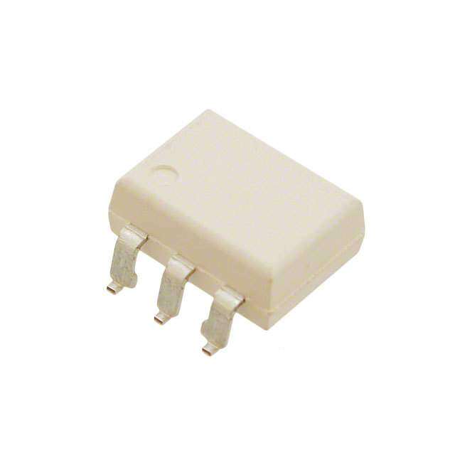
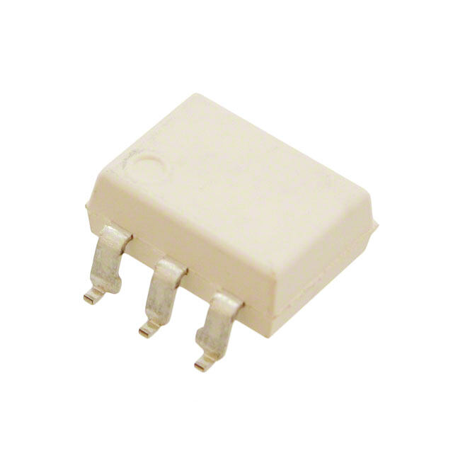
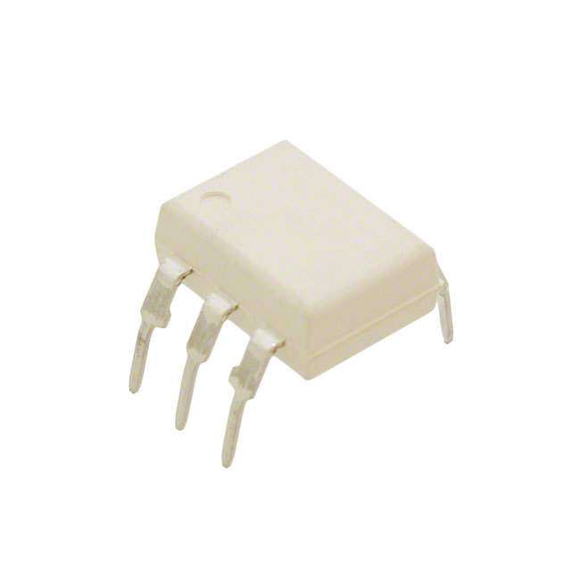
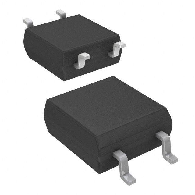
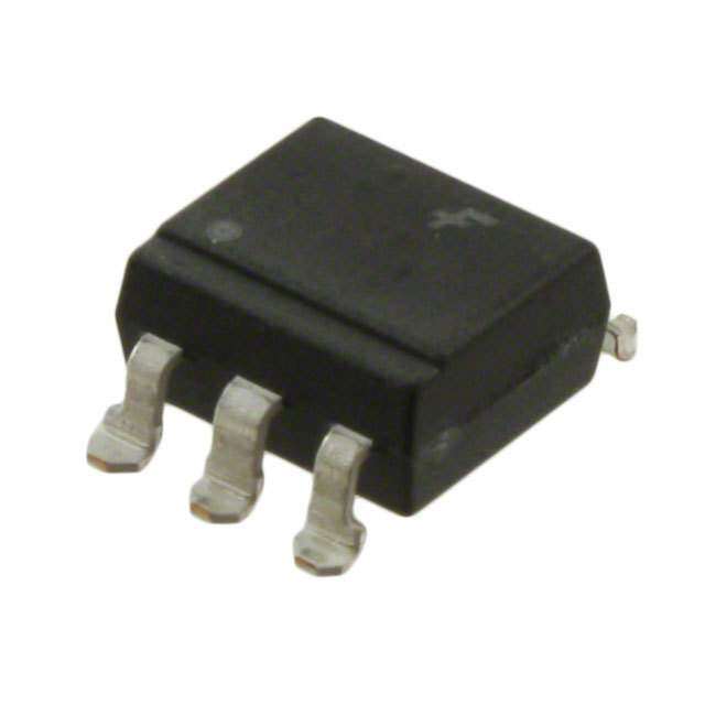
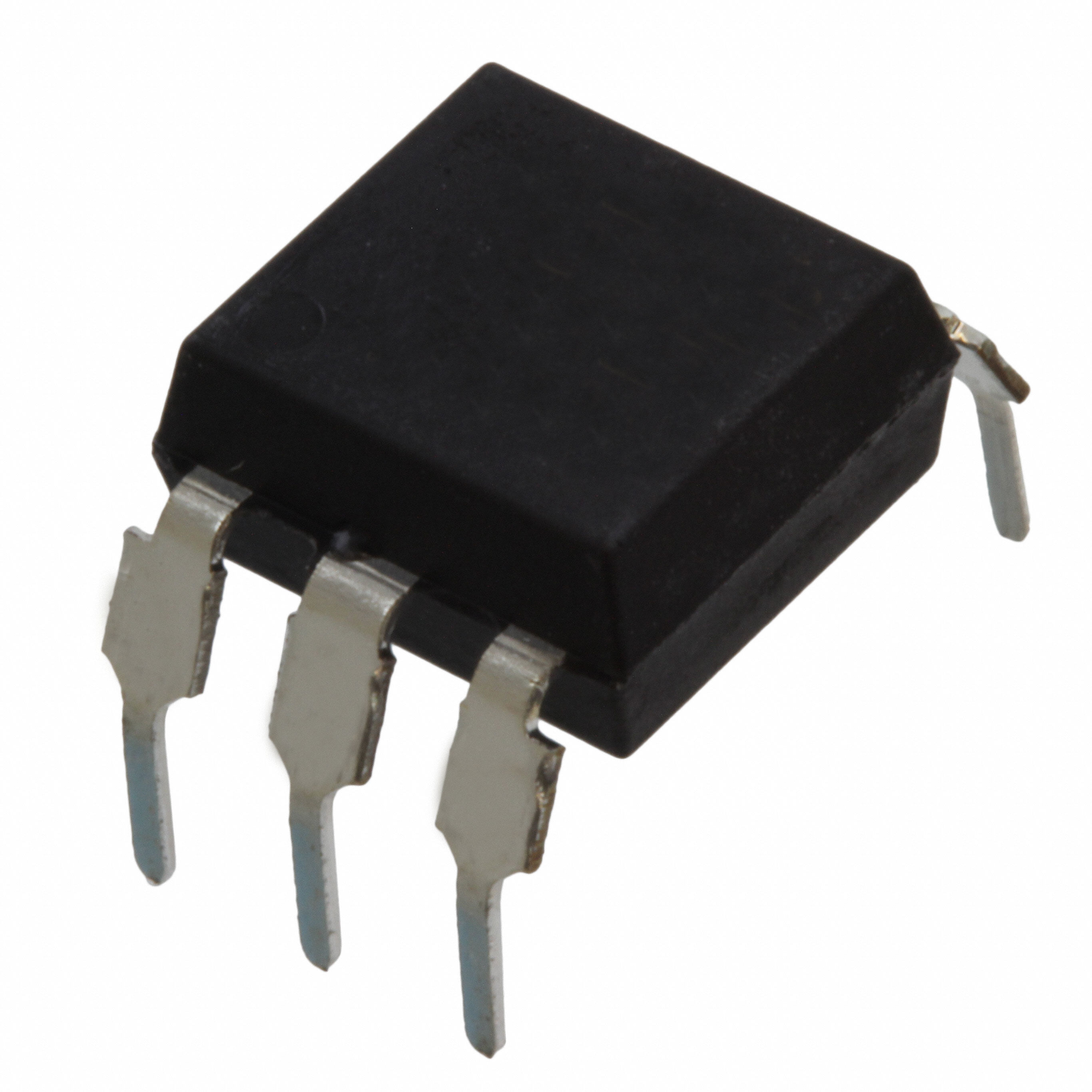
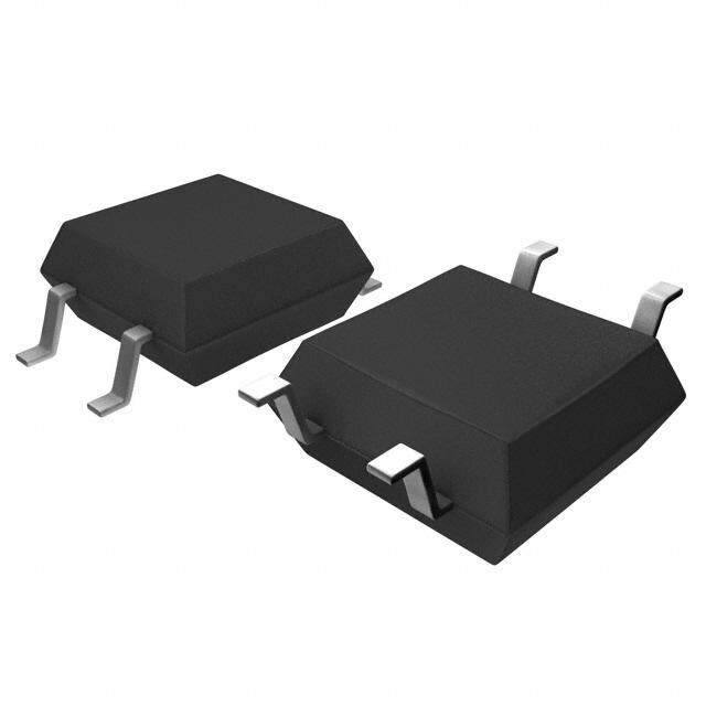
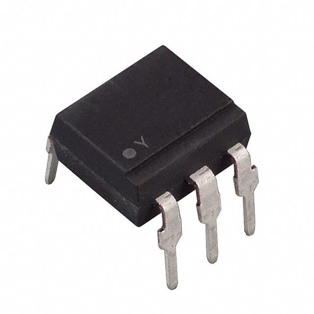
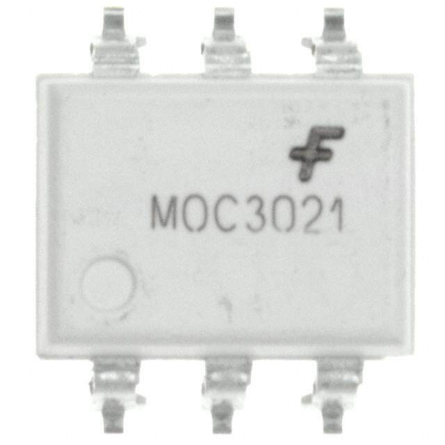
| 描述 | OPTOCOUPLER TRIAC 600V 6DIP ZC三极与 SCR 输出光电耦合器 6Pin600V Optocoupler Zero Cross Triac Dr |
| 产品分类 | |
| 品牌 | Fairchild Semiconductor |
| 产品手册 | |
| 产品图片 |
|
| rohs | 符合RoHS无铅 / 符合限制有害物质指令(RoHS)规范要求 |
| 产品系列 | 光耦合器/光电耦合器,三极与 SCR 输出光电耦合器,Fairchild Semiconductor MOC3063TVM- |
| 数据手册 | |
| 产品型号 | MOC3063TVM |
| 产品目录页面 | |
| 产品种类 | 三极与 SCR 输出光电耦合器 |
| 供应商器件封装 | 6-DIP |
| 关断状态下输出电压-VDRM | 600 V |
| 功率耗散 | 250 mW |
| 包装 | 管件 |
| 单位重量 | 864 mg |
| 商标 | Fairchild Semiconductor |
| 安装类型 | 通孔 |
| 封装 | Bulk |
| 封装/外壳 | 6-DIP(0.400",10.16mm) |
| 封装/箱体 | PDIP-6 |
| 工厂包装数量 | 1000 |
| 最大工作温度 | + 85 C |
| 最大触发电流 | 5 mA |
| 最小工作温度 | - 40 C |
| 标准包装 | 1,000 |
| 正向电压 | 1.3 V |
| 正向电流 | 60 mA |
| 每芯片的通道数量 | 1 Channel |
| 电压-断态 | 600V |
| 电压-正向(Vf)(典型值) | 1.3V |
| 电压-隔离 | 7500Vpk |
| 电流-DC正向(If) | 60mA |
| 电流-保持(Ih) | 500µA (标准) |
| 电流-栅极触发(Igt)(最大值) | 5mA |
| 电流-输出/通道 | - |
| 系列 | MOC3063TM |
| 绝缘电压 | 5250 Vrms |
| 认可 | UR, VDE |
| 输出类型 | AC |
| 输出设备 | PhotoTriac |
| 通道数 | 1 |
| 零交叉电压 | 20 V |
| 零交叉电路 | With Zero-Crossing Circuit |
| 零件号别名 | MOC3063TVM_NL |
-angle.jpg)


.jpg)

- 商务部:美国ITC正式对集成电路等产品启动337调查
- 曝三星4nm工艺存在良率问题 高通将骁龙8 Gen1或转产台积电
- 太阳诱电将投资9.5亿元在常州建新厂生产MLCC 预计2023年完工
- 英特尔发布欧洲新工厂建设计划 深化IDM 2.0 战略
- 台积电先进制程称霸业界 有大客户加持明年业绩稳了
- 达到5530亿美元!SIA预计今年全球半导体销售额将创下新高
- 英特尔拟将自动驾驶子公司Mobileye上市 估值或超500亿美元
- 三星加码芯片和SET,合并消费电子和移动部门,撤换高东真等 CEO
- 三星电子宣布重大人事变动 还合并消费电子和移动部门
- 海关总署:前11个月进口集成电路产品价值2.52万亿元 增长14.8%


PDF Datasheet 数据手册内容提取
Is Now Part of To learn more about ON Semiconductor, please visit our website at www.onsemi.com Please note: As part of the Fairchild Semiconductor integration, some of the Fairchild orderable part numbers will need to change in order to meet ON Semiconductor’s system requirements. Since the ON Semiconductor product management systems do not have the ability to manage part nomenclature that utilizes an underscore (_), the underscore (_) in the Fairchild part numbers will be changed to a dash (-). This document may contain device numbers with an underscore (_). Please check the ON Semiconductor website to verify the updated device numbers. The most current and up-to-date ordering information can be found at www.onsemi.com. Please email any questions regarding the system integration to Fairchild_questions@onsemi.com. ON Semiconductor and the ON Semiconductor logo are trademarks of Semiconductor Components Industries, LLC dba ON Semiconductor or its subsidiaries in the United States and/or other countries. ON Semiconductor owns the rights to a number of patents, trademarks, copyrights, trade secrets, and other intellectual property. A listing of ON Semiconductor’s product/patent coverage may be accessed at www.onsemi.com/site/pdf/Patent-Marking.pdf. ON Semiconductor reserves the right to make changes without further notice to any products herein. ON Semiconductor makes no warranty, representation or guarantee regarding the suitability of its products for any particular purpose, nor does ON Semiconductor assume any liability arising out of the application or use of any product or circuit, and specifically disclaims any and all liability, including without limitation special, consequential or incidental damages. Buyer is responsible for its products and applications using ON Semiconductor products, including compliance with all laws, regulations and safety requirements or standards, regardless of any support or applications information provided by ON Semiconductor. “Typical” parameters which may be provided in ON Semiconductor data sheets and/or specifications can and do vary in different applications and actual performance may vary over time. All operating parameters, including “Typicals” must be validated for each customer application by customer’s technical experts. ON Semiconductor does not convey any license under its patent rights nor the rights of others. ON Semiconductor products are not designed, intended, or authorized for use as a critical component in life support systems or any FDA Class 3 medical devices or medical devices with a same or similar classification in a foreign jurisdiction or any devices intended for implantation in the human body. Should Buyer purchase or use ON Semiconductor products for any such unintended or unauthorized application, Buyer shall indemnify and hold ON Semiconductor and its officers, employees, subsidiaries, affiliates, and distributors harmless against all claims, costs, damages, and expenses, and reasonable attorney fees arising out of, directly or indirectly, any claim of personal injury or death associated with such unintended or unauthorized use, even if such claim alleges that ON Semiconductor was negligent regarding the design or manufacture of the part. ON Semiconductor is an Equal Opportunity/Affirmative Action Employer. This literature is subject to all applicable copyright laws and is not for resale in any manner.
M O C September 2015 3 0 6 X M , MOC3061M, MOC3062M, MOC3063M, M O MOC3162M, MOC3163M C 3 1 6-Pin DIP Zero-Cross Triac Driver Optocoupler (600 Volt Peak) 6 X M Features Description — 6 • Simplifies Logic Control of 115/240 VAC Power The MOC306XM and MOC316XM devices consist of a - P • Zero Voltage Crossing to Minimize Conducted and GaAs infrared emitting diode optically coupled to a i n Radiated Line Noise monolithic silicon detector performing the function of a D zero voltage crossing bilateral triac driver. • 600 V Peak Blocking Voltage IP • Superior Static dv/dt They are designed for use with a triac in the interface of Z – 600 V/μs (MOC306xM) logic systems to equipment powered from 115/240 VAC er lines, such as solid-state relays, industrial controls, o – 1000 V/μs (MOC316xM) - motors, solenoids and consumer appliances, etc. C • Safety and Regulatory Approvals r o – UL1577, 4,170 VAC for 1 Minute s RMS s – DIN EN/IEC60747-5-5 T r i Applications a c • Solenoid/Valve Controls D r • Static Power Switches iv e • Temperature Controls r O • AC Motor Starters p • Lighting Controls t o • AC Motor Drives c o • E.M. Contactors u p • Solid State Relays l e r ( 6 0 0 Schematic Package Outlines V o l t P e a k ANODE 1 6 MAIN TERM. ) CATHODE 2 5 NC* ZERO N/C 3 CROSSING 4 MAIN TERM. CIRCUIT *DO NOT CONNECT (TRIAC SUBSTRATE) Figure 1. Schematic Figure 2. Package Outlines ©2005 Fairchild Semiconductor Corporation www.fairchildsemi.com MOC306XM, MOC316XM Rev. 1.5
M O Safety and Insulation Ratings C 3 As per DIN EN/IEC 60747-5-5, this optocoupler is suitable for “safe electrical insulation” only within the safety limit 0 6 data. Compliance with the safety ratings shall be ensured by means of protective circuits. X M Parameter Characteristics , M Installation Classifications per DIN VDE < 150 VRMS I–IV O 0110/1.89 Table 1, For Rated Mains Voltage < 300 V I–IV C RMS 3 Climatic Classification 40/85/21 1 6 X Pollution Degree (DIN VDE 0110/1.89) 2 M Comparative Tracking Index 175 — 6 - P Symbol Parameter Value Unit in D Input-to-Output Test Voltage, Method A, V x 1.6 = V , Type and Sample Test with t = 10 s, PartIiOaRl DMischarge <P R5 pC 1360 Vpeak IP m V Z PR Input-to-Output Test Voltage, Method B, V x 1.875 = V , e 100% Production Test with t = 1 s, PartiaIlO DRiMscharge < 5 pPCR 1594 Vpeak ro m - C V Maximum Working Insulation Voltage 850 V IORM peak r o VIOTM Highest Allowable Over-Voltage 6000 Vpeak s s External Creepage ≥ 7 mm T External Clearance ≥ 7 mm ri a c External Clearance (for Option TV, 0.4" Lead Spacing) ≥ 10 mm D DTI Distance Through Insulation (Insulation Thickness) ≥ 0.5 mm r i v R Insulation Resistance at T , V = 500 V > 109 Ω e IO S IO r O p t o c o u p l e r ( 6 0 0 V o l t P e a k ) ©2005 Fairchild Semiconductor Corporation www.fairchildsemi.com MOC306XM, MOC316XM Rev. 1.5 2
M O Absolute Maximum Ratings C Stresses exceeding the absolute maximum ratings may damage the device. The device may not function or be 3 0 operable above the recommended operating conditions and stressing the parts to these levels is not recommended. 6 X In addition, extended exposure to stresses above the recommended operating conditions may affect device reliability. M The absolute maximum ratings are stress ratings only. T = 25°C unless otherwise specified. A , M Symbol Parameters Device Value Unit O C TOTAL DEVICE 3 1 TSTG Storage Temperature All -40 to +150 °C 6 X TOPR Operating Temperature All -40 to +85 °C M T Junction Temperature Range All -40 to +100 °C — J 260 for 6 T Lead Solder Temperature All °C - SOL 10 seconds P i n Total Device Power Dissipation at 25°C Ambient 250 mW P All D D Derate Above 25°C 2.94 mW/°C IP EMITTER Z e IF Continuous Forward Current All 60 mA ro - V Reverse Voltage All 6 V C R r Total Power Dissipation at 25°C Ambient 120 mW o P All s D s Derate Above 25°C 1.41 mW/°C T DETECTOR r i a V Off-State Output Terminal Voltage All 600 V c DRM D Peak Non-Repetitive Surge Current r ITSM (Single Cycle 60 Hz Sine Wave) All 1 A iv e Total Power Dissipation at 25°C Ambient 150 mW r P All O D Derate Above 25°C 1.76 mW/°C p t o c o u p l e r ( 6 0 0 V o l t P e a k ) ©2005 Fairchild Semiconductor Corporation www.fairchildsemi.com MOC306XM, MOC316XM Rev. 1.5 3
M O Electrical Characteristics C T = 25°C unless otherwise specified. 3 A 0 Individual Component Characteristics 6 X M Symbol Parameters Test Conditions Device Min. Typ. Max. Unit , M EMITTER O C V Input Forward Voltage I = 30 mA All 1.3 1.5 V F F 3 I Reverse Leakage Current V = 6 V All 0.005 100 μA 1 R R 6 X DETECTOR M Peak Blocking Current, MOC306XM 10 500 — I V = 600 V, I = 0(1) nA DRM1 Either Direction DRM F MOC316XM 10 100 6 - Critical Rate of Rise of MOC306XM 600 1500 P dv/dt Off-State Voltage IF = 0 (Figure 11)(2) MOC316XM 1000 V/μs in D I P Transfer Characteristics Z e Symbol DC Characteristics Test Conditions Device Min. Typ. Max. Unit r o MOC3061M 15 -C r MOC3062M o LED Trigger Current Main Terminal 10 s IFT (Rated I ) Voltage = 3 V(3) MOC3162M mA s FT T MOC3063M r 5 i MOC3163M a c I = 100 mA peak, D VTM Peak On-State Voltage, Either Direction ITF M= rated IFT All 1.8 3.0 V riv I Holding Current, Either Direction All 500 μA e H r O p Zero Crossing Characteristics t o Symbol Characteristics Test Conditions Device Min. Typ. Max. Unit c o u MOC3061M p Inhibit Voltage (MT1-MT2 MOC3062M 12 20 le r VINH voltage above which IF = rated IFT MOC3063M V (6 device will not trigger) MOC3162M 0 12 15 0 MOC3163M V o I Leakage in Inhibited IF = rated IFT, DRM = 600 V, All 2 mA lt DRM2 State off-state P e a Isolation Characteristics k ) Symbol Parameter Test Conditions Min. Typ. Max. Unit V Isolation Voltage(4) f = 60 Hz, t = 1 Minute 4170 VAC ISO RMS R Isolation Resistance V = 500 V 1011 Ω ISO I-O DC C Isolation Capacitance V = 0 V, f = 1 MHz 0.2 pF ISO Notes: 1. Test voltage must be applied within dv/dt rating. 2. This is static dv/dt. See Figure 11 for test circuit. Commutating dv/dt is a function of the load-driving thyristor(s) only. 3. All devices are guaranteed to trigger at an I value less than or equal to max I . Therefore, recommended operating F FT I lies between max I (15 mA for MOC3061M, 10 mA for MOC3062M and MOC3162M, 5 mA for MOC3063M and F FT MOC3163M) and absolute maximum I (60 mA). F 4. Isolation voltage, V , is an internal device dielectric breakdown rating. For this test, pins 1 and 2 are common, and ISO pins 4, 5 and 6 are common. ©2005 Fairchild Semiconductor Corporation www.fairchildsemi.com MOC306XM, MOC316XM Rev. 1.5 4
M O Typical Performance Curves C 3 0 6 1.7 1.6 X M 1.6 , 1.5 VTM = 3V M GE (V) 11..45 1.4 NORMALIZED TO TA = 25°C OC3 LTA 1.3 ED 1.3 16 RD VO 1.2 TA = -40°C MALIZ 1.2 XM RWA 1.1 TA = 25°C NOR — O , T 1.1 6 V, FF 1.0 TA = 85°C IF -P 1.0 i 0.9 n D 0.8 0.9 I P 0.7 Z 0.1 1 10 100 0.8 e -40 -20 0 20 40 60 80 100 r IF, LED FORWARD CURRENT (mA) TA, AMBIENT TEMPERATURE (°C) o- C Figure 3. LED Forward Voltage vs. Forward Current Figure 4. Trigger Current Vs. Temperature r o s s T r 16 10000 ia c ED) 14 D NT (NORMALIZ 1102 TNAO =R M25A°LCIZED TO PWIN >> 100μs RRENT (nA) 1010000 river Op E U t R C o UR 8 GE c C A o R K 10 u D TRIGGE 46 I, LEADRM 1 pler ( E 6 , LT 2 00 IF 0.1 V 0 -40 -20 0 20 40 60 80 100 o 1 10 100 l PWIN, LED TRIGGER PULSE WIDTH (μs) TA, AMBIENT TEMPERATURE (°C) t P e Figure 5. LED Current Required to Trigger vs. Figure 6. Leakage Current, IDRM vs. Temperature a LED Pulse Width k ) ©2005 Fairchild Semiconductor Corporation www.fairchildsemi.com MOC306XM, MOC316XM Rev. 1.5 5
M O Typical Performance Curves (Continued) C 3 0 6 X 2.4 800 M 2.2 INFO =R RMAATLEIZDE IDFT TO TA = 25°C 600 , M 2.0 TA = 25°C O mA) 400 C 1.8 T ( 3 ED 1.6 EN 200 16 LIZ RR X MA 1.4 CU 0 M R E O 1.2 T — N A I, DRM2 01..80 , ON-STTM --420000 6-Pin I 0.6 -600 D I P 0.4 -40 -20 0 20 40 60 80 100 -800 Z -4 -3 -2 -1 0 1 2 3 4 e TA, AMBIENT TEMPERATURE (°C) VTM, ON-STATE VOLTAGE (VOLTS) ro - Figure 7. IDRM2, Leakage in Inhibit State vs. Temperature Figure 8. On-State Characteristics C r o s s 3.2 1.20 T r i ED) 2.8 1.15 NORMALIZED TO TA = 25°C ac MALIZ 2.4 D 1.10 Driv G CURRENT (NOR 112...260 , NORMALIZEVINH 011...900505 er Optoco N 0.90 u DI p HOL 0.8 0.85 le I, H 0.4 0.80 r (6 -40 -20 0 20 40 60 80 100 0 0 0.0 TA, AMBIENT TEMPERATURE (°C) -40 -20 0 20 40 60 80 100 V o TA, AMBIENT TEMPERATURE (°C) lt Figure 9. IH, Holding Current vs. Temperature Figure 10. Inhibit Voltage vs. Temperature P e a k ) ©2005 Fairchild Semiconductor Corporation www.fairchildsemi.com MOC306XM, MOC316XM Rev. 1.5 6
M O 1. 100x scope probes are used, to allow high speeds and voltages. C 2. The worst-case condition for static dv/dt is established by triggering the D.U.T. with a normal LED input current, then 3 0 removing the current. The variable vernier resistor combined with various capacitor combinations allows the dv/dt to 6 X be gradually increased until the D.U.T. continues to trigger in response to the applied voltage pulse, even after the M LED current has been removed. The dv/dt is then decreased until the D.U.T. stops triggering. t is measured at this RC , point and recorded. M O 27Ω C VDRM/VRRM SELECT 2W 1000Ω 3 10 WATT 1 X100 PROBE 6 WIREWOUND 6 1 X DIFPFREERAEMNTPIAL 2 DUT 20kΩ 2W 0.33μF 1000V 0.047μF M X100 PROBE 4 1000V — 470pF 6 - dV P MTEOMUPNETR DAUTTU ROEN CONTROLLED VERdNtIER 100Ω 0.001μF in Cμ PLATE 2W D 0.005μF 1 MΩ 12.W2 MEAΩCH IP 82Ω 0.01μF Z 2W POWER 2W e 0.047μF TEST ro - C 1N914 0.1μF r o 20V RFP4N100 0.47μF 0-1000V ss 56Ω 1000Ω 10mA T fP =W 1 =0 1H0z0 μs 2W 1/4W 1N1986V7A ria 50 Ω PULSE c GENERATOR D r ALL COMPONENTS ARE NON-INDUCTIVE UNLESS SHOWN i v dV Figure 11. Circuit for Static Measurement of Power Thyristors e ddVt r O p Basic Applications t o c Typical circuit for use when hot line switching is o u required. In this circuit the “hot” side of the line is p switched and the load connected to the cold or le neutral side. The load may be connected to either r ( the neutral or hot line. Rin 1 6 360Ω 6 VCC HOT 0 FKPF12N60 0 oRfi nt hise cpaalrctu, l1a5temdA s ofo trh tahte I FM iOs Ceq3u0a6l1 tMo ,t h1e0 mraAte fdo rIF T 2 MMMOOOCCC333000666123MMM 5 39Ω Vo the MOC3062M, or 5mA for the MOC3063M. 3 4 240 VAC lt The 39Ω resistor and 0.01μF capacitor are for 360Ω 0.01μF P e snubbing of the triac and is often, but not always, LOAD NEUTRAL a necessary depending upon the particular triac and k ) Figure 12. Hot-Line Switching Application Circuit load used. Suggested method of firing two, back-to-back SCR’s with a Fairchild triac driver. Diodes can be 1N4001; resistors, R1 and R2, are 115 VAC optional 330Ω. R1 D1 1 6 Note: VCC This optoisolator should not be used to drive Rin 2 MMOOCC33006612MM 5 SCR a load directly. It is intended to be a trigger 3 MOC3063M 4 360Ω SCR device only. R2 D2 LOAD Figure 13. Inverse-Parallel SCR Driver Circuit ©2005 Fairchild Semiconductor Corporation www.fairchildsemi.com MOC306XM, MOC316XM Rev. 1.5 7
M O Reflow Profile C 3 0 Max. Ramp-up Rate = 3°C/S 6 TP Max. Ramp-down Rate = 6°C/S X 260 M 240 tP , TL M 220 O 200 Tsmax C tL 3 ) 180 Preheat Area 1 C 6 ° 160 X e ( 140 Tsmin M ur ts — t 120 a er 100 6- p P m 80 i n Te 60 D 40 IP 20 Z e 0 r o 120 240 360 - C Time 25°C to Peak ro s Time (seconds) s T r i a c Profile Freature Pb-Free Assembly Profile D r i Temperature Minimum (Tsmin) 150°C v e Temperature Maximum (Tsmax) 200°C r O Time (t ) from (Tsmin to Tsmax) 60 seconds to 120 seconds p S t o Ramp-up Rate (T to T ) 3°C/second maximum L P c o Liquidous Temperature (TL) 217°C u p Time (tL) Maintained Above (TL) 60 seconds to 150 seconds le Peak Body Package Temperature 260°C +0°C / –5°C r ( 6 Time (tP) within 5°C of 260°C 30 seconds 0 0 Ramp-down Rate (TP to TL) 6°C/second maximum V o Time 25°C to Peak Temperature 8 minutes maximum l t P e Figure 14. Reflow Profile a k ) ©2005 Fairchild Semiconductor Corporation www.fairchildsemi.com MOC306XM, MOC316XM Rev. 1.5 8
M O Ordering Information(5) C 3 0 Part Number Package Packing Method 6 X MOC3061M DIP 6-Pin Tube (50 Units) M , MOC3061SM SMT 6-Pin (Lead Bend) Tube (50 Units) M O MOC3061SR2M SMT 6-Pin (Lead Bend) Tape and Reel (1000 Units) C MOC3061VM DIP 6-Pin, DIN EN/IEC60747-5-5 Option Tube (50 Units) 3 1 6 MOC3061SVM SMT 6-Pin (Lead Bend), DIN EN/IEC60747-5-5 Option Tube (50 Units) X M MOC3061SR2VM SMT 6-Pin (Lead Bend), DIN EN/IEC60747-5-5 Option Tape and Reel (1000 Units) — MOC3061TVM DIP 6-Pin, 0.4” Lead Spacing, DIN EN/IEC60747-5-5 Option Tube (50 Units) 6 Note: - P 5. The product orderable part number system listed in this table also applies to the MOC3062M, MOC3063M, in MOC3162M, and MOC3163M product families. D I P Z Marking Information e r o - C r o 1 s s T r MOC3061 2 i a c D V X YY Q 6 r i v e r O 3 4 5 p t o c Figure 15. Top Mark o u p l e r ( Top Mark Definitions 6 0 0 1 Fairchild Logo V o 2 Device Number l t DIN EN/IEC60747-5-5 Option (only appears on component P 3 e ordered with this option) a k 4 One-Digit Year Code, e.g., ‘5’ ) 5 Two-Digit Work Week, Ranging from ‘01’ to ‘53’ 6 Assembly Package Code ©2005 Fairchild Semiconductor Corporation www.fairchildsemi.com MOC306XM, MOC316XM Rev. 1.5 9
None
None
None
ON Semiconductor and are trademarks of Semiconductor Components Industries, LLC dba ON Semiconductor or its subsidiaries in the United States and/or other countries. ON Semiconductor owns the rights to a number of patents, trademarks, copyrights, trade secrets, and other intellectual property. A listing of ON Semiconductor’s product/patent coverage may be accessed at www.onsemi.com/site/pdf/Patent−Marking.pdf. ON Semiconductor reserves the right to make changes without further notice to any products herein. ON Semiconductor makes no warranty, representation or guarantee regarding the suitability of its products for any particular purpose, nor does ON Semiconductor assume any liability arising out of the application or use of any product or circuit, and specifically disclaims any and all liability, including without limitation special, consequential or incidental damages. Buyer is responsible for its products and applications using ON Semiconductor products, including compliance with all laws, regulations and safety requirements or standards, regardless of any support or applications information provided by ON Semiconductor. “Typical” parameters which may be provided in ON Semiconductor data sheets and/or specifications can and do vary in different applications and actual performance may vary over time. All operating parameters, including “Typicals” must be validated for each customer application by customer’s technical experts. ON Semiconductor does not convey any license under its patent rights nor the rights of others. ON Semiconductor products are not designed, intended, or authorized for use as a critical component in life support systems or any FDA Class 3 medical devices or medical devices with a same or similar classification in a foreign jurisdiction or any devices intended for implantation in the human body. Should Buyer purchase or use ON Semiconductor products for any such unintended or unauthorized application, Buyer shall indemnify and hold ON Semiconductor and its officers, employees, subsidiaries, affiliates, and distributors harmless against all claims, costs, damages, and expenses, and reasonable attorney fees arising out of, directly or indirectly, any claim of personal injury or death associated with such unintended or unauthorized use, even if such claim alleges that ON Semiconductor was negligent regarding the design or manufacture of the part. ON Semiconductor is an Equal Opportunity/Affirmative Action Employer. This literature is subject to all applicable copyright laws and is not for resale in any manner. PUBLICATION ORDERING INFORMATION LITERATURE FULFILLMENT: N. American Technical Support: 800−282−9855 Toll Free ON Semiconductor Website: www.onsemi.com Literature Distribution Center for ON Semiconductor USA/Canada 19521 E. 32nd Pkwy, Aurora, Colorado 80011 USA Europe, Middle East and Africa Technical Support: Order Literature: http://www.onsemi.com/orderlit Phone: 303−675−2175 or 800−344−3860 Toll Free USA/Canada Phone: 421 33 790 2910 Fax: 303−675−2176 or 800−344−3867 Toll Free USA/Canada Japan Customer Focus Center For additional information, please contact your local Email: orderlit@onsemi.com Phone: 81−3−5817−1050 Sales Representative © Semiconductor Components Industries, LLC www.onsemi.com www.onsemi.com 1
Mouser Electronics Authorized Distributor Click to View Pricing, Inventory, Delivery & Lifecycle Information: O N Semiconductor: MOC3063SR2M MOC3063M MOC3063SR2VM MOC3063VM MOC3063SM MOC3063TVM MOC3063SVM