ICGOO在线商城 > 分立半导体产品 > 晶体管 - 双极 (BJT) - 单 > FZT869TA

 Datasheet下载
- 型号: FZT869TA
- 制造商: Diodes Inc.
- 库位|库存: xxxx|xxxx
- 要求:
| 数量阶梯 | 香港交货 | 国内含税 |
| +xxxx | $xxxx | ¥xxxx |
查看当月历史价格
查看今年历史价格
FZT869TA产品简介:
ICGOO电子元器件商城为您提供FZT869TA由Diodes Inc.设计生产,在icgoo商城现货销售,并且可以通过原厂、代理商等渠道进行代购。 FZT869TA价格参考。Diodes Inc.FZT869TA封装/规格:晶体管 - 双极 (BJT) - 单, 双极 (BJT) 晶体管 NPN 25V 7A 100MHz 3W 表面贴装 SOT-223。您可以下载FZT869TA参考资料、Datasheet数据手册功能说明书,资料中有FZT869TA 详细功能的应用电路图电压和使用方法及教程。
FZT869TA 是由 Diodes Incorporated 生产的一款双极型晶体管(BJT),属于单晶体管类型。该型号的晶体管通常适用于以下场景:

1. 开关电路:FZT869TA 可以用作电子开关,控制其他设备的开启和关闭。例如,在继电器驱动、LED 控制或电机启动等应用中,它能够高效地切换电流。

2. 信号放大:作为一款 BJT 晶体管,FZT869TA 具备良好的信号放大能力,适合用于音频放大器、射频(RF)放大器或其他需要低噪声放大的场合。

3. 电源管理:在一些简单的电源管理电路中,如稳压器或电流限制电路,FZT869TA 可以起到关键作用,帮助调节输出电压或电流。

4. 传感器接口:此晶体管可以用来增强传感器输出信号的强度,使其能够驱动后续的处理电路或显示设备。

5. 脉宽调制 (PWM) 应用:在 PWM 控制电路中,FZT869TA 能够根据输入的 PWM 信号调整负载的功率,常用于亮度调节、速度控制等领域。

具体选择 FZT869TA 时,需考虑其电气参数是否满足实际需求,包括集电极-发射极击穿电压、最大集电极电流、直流电流增益等。此外,确保工作环境温度范围符合器件规格也是重要的考量因素。总之,FZT869TA 凭借其性能特点,在多种中小型功率电子应用中表现出色。
| 参数 | 数值 |
| 产品目录 | |
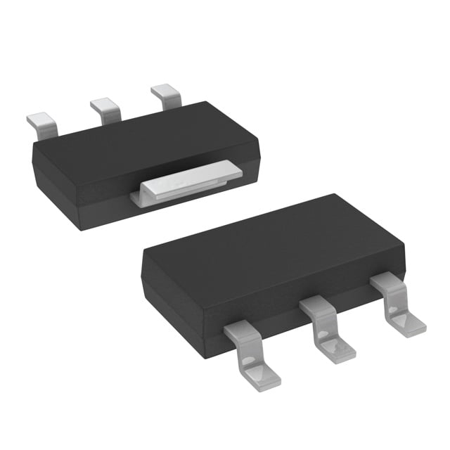
| 描述 | TRANS NPN 25V 7000MA SOT-223两极晶体管 - BJT NPN High Ct Low Sat |
| 产品分类 | 晶体管(BJT) - 单路分离式半导体 |
| 品牌 | Diodes Incorporated |
| 产品手册 | |
| 产品图片 |
|
| rohs | 符合RoHS无铅 / 符合限制有害物质指令(RoHS)规范要求 |
| 产品系列 | 晶体管,两极晶体管 - BJT,Diodes Incorporated FZT869TA- |
| 数据手册 | |
| 产品型号 | FZT869TA |
| PCN其它 | |
| RoHS指令信息 | http://diodes.com/download/4349 |
| 不同 Ib、Ic时的 Vce饱和值(最大值) | 350mV @ 150mA,6.5A |
| 不同 Ic、Vce 时的DC电流增益(hFE)(最小值) | 300 @ 1A,1V |
| 产品目录绘图 |
|
| 产品目录页面 | |
| 产品种类 | 两极晶体管 - BJT |
| 供应商器件封装 | SOT-223 |
| 其它名称 | FZT869 |
| 功率-最大值 | 3W |
| 包装 | 剪切带 (CT) |
| 发射极-基极电压VEBO | 6 V |
| 商标 | Diodes Incorporated |
| 增益带宽产品fT | 100 MHz |
| 安装类型 | 表面贴装 |
| 安装风格 | SMD/SMT |
| 封装 | Reel |
| 封装/外壳 | TO-261-4,TO-261AA |
| 封装/箱体 | SOT-223 |
| 工厂包装数量 | 1000 |
| 晶体管极性 | NPN |
| 晶体管类型 | NPN |
| 最大功率耗散 | 3 W |
| 最大工作温度 | + 150 C |
| 最大直流电集电极电流 | 7 A |
| 最小工作温度 | - 55 C |
| 标准包装 | 1 |
| 电压-集射极击穿(最大值) | 25V |
| 电流-集电极(Ic)(最大值) | 7A |
| 电流-集电极截止(最大值) | - |
| 直流电流增益hFE最大值 | 300 |
| 直流集电极/BaseGainhfeMin | 300 at 10 mA at 1 V, 300 at 1 A at 1 V, 200 at 7 A at 1 V, 40 at 20 A at 1 V |
| 系列 | FZT869 |
| 配置 | Single |
| 集电极—发射极最大电压VCEO | 25 V |
| 集电极—基极电压VCBO | 60 V |
| 频率-跃迁 | 100MHz |


PDF Datasheet 数据手册内容提取
FZT869 Green 25V NPN HIGH CURRENT TRANSI STOR IN SOT223 Features Mechanical Data BVCEO > 25V Case: SOT223 IC = 7A High Continuous Collector Current Case Material: Molded Plastic. “Green” Molding Compound. ICM = 20A Peak Pulse Current UL Flammability Rating 94V-0 Very Low Saturation Voltage VCE(SAT) < 110mV @ 1A Moisture Sensitivity: Level 1 per J-STD-020 RCE(SAT) = 36mΩ at 5A for a Low Equivalent On-Resistance Terminals: Finish - Matte Tin Plated Leads. hFE Specified Up to 20A for a High Gain Hold Up Solderable per MIL-STD-202, Method 208 e3 PTOT = 3W Weight: 0.112 grams (Approximate) Lead-Free Finish; RoHS Compliant (Notes 1 & 2) Halogen and Antimony Free. “Green” Device (Note 3) Qualified to AEC-Q101 Standards for High Reliability SOT223 C B E Top View Top View Device Symbol Pin-Out Ordering Information (Note 4) Product Compliance Marking Reel Size (inches) Tape Width (mm) Quantity per Reel FZT869TA AEC-Q101 FZT869 7 12 1,000 Notes: 1. EU Directive 2002/95/EC (RoHS) & 2011/65/EU (RoHS 2) compliant. All applicable RoHS exemptions applied. 2. See https://www.diodes.com/quality/lead-free/ for more information about Diodes Incorporated’s definitions of Halogen- and Antimony-free, "Green" and Lead-free. 3. Halogen- and Antimony-free "Green” products are defined as those which contain <900ppm bromine, <900ppm chlorine (<1500ppm total Br + Cl) and <1000ppm antimony compounds. 4. For packaging details, go to our website at https://www.diodes.com/design/support/packaging/diodes-packaging/. Marking Information SOT223 FZT 869 = Product Type Marking Code FZT W YWW = Date Code Marking W Y or Y = Last Digit of Year (ex: 7 = 2017) 869 Y WW or WW = Week Code (01–53) FZT869 1 of 7 March 2017 Document Number DS33178 Rev. 4 - 2 www.diodes.com © Diodes Incorporated
FZT869 Absolute Maximum Ratings (@TA = +25°C, unless otherwise specified.) Characteristic Symbol Value Unit Collector-Base Voltage VCBO 60 V Collector-Emitter Voltage VCEO 25 V Emitter-Base Voltage VEBO 6 V Continuous Collector Current IC 7 A Peak Pulse Current ICM 20 A Thermal Characteristics (@TA = +25°C, unless otherwise specified.) Characteristic Symbol Value Unit 3 (Note 5) Power Dissipation 24 W Linear Derating Factor PD 1.6 mW/°C (Note 6) 12.8 Thermal Resistance, Junction to Ambient (Note 5) RθJA 42 (Note 6) RθJA 78 °C/W Thermal Resistance Junction to Lead (Note 7) RθJL 8.8 Operating and Storage Temperature Range TJ, TSTG -55 to +150 °C ESD Ratings (Note 8) Characteristic Symbol Value Unit JEDEC Class Electrostatic Discharge - Human Body Model ESD HBM 4,000 V 3A Electrostatic Discharge - Machine Model ESD MM 400 V C Notes: 5. For a device mounted with the collector lead on 52mm x 52mm 2oz copper that is on a single-sided 1.6mm FR4 PCB; device is measured under still air conditions whilst operating in steady-state. 6. Same as note (5), except the device is mounted on 25mm x 25mm 1oz copper. 7. Thermal resistance from junction to solder-point (at the end of the collector lead). 8. Refer to JEDEC specification JESD22-A114 and JESD22-A115. FZT869 2 of 7 March 2017 Document Number DS33178 Rev. 4 - 2 www.diodes.com © Diodes Incorporated
FZT869 Thermal Characteristics and Derating Information A) 10 VLiCmE(istat) W) 3.0 ent ( on ( 2.5 5si2nmglem sXi5de2dm 2moz Cu r 1 ti 2.0 r DC a u p r C 1s ssi 1.5 to 100ms Di c100m 10ms 1.0 e r oll Single Pulse. Tamb=25°C 1ms we 25mmX25mm CC sin5g2lem smidXe5d2 2momz Cu 100µs Po 0.5 single sided 1oz Cu I10m x 0.0 - a 100m 1 10 100 0 20 40 60 80 100 120 140 160 M -V Collector-Emitter Voltage (V) Temperature (°C) CE Safe Operating Area Derating Curve 52mmX52mm Single Pulse. T =25°C ) 40 ) amb W single sided 2oz Cu W 52mmX52mm 100 C/ ( single sided 2oz Cu n e (° 30 atio c D=0.5 p esistan 20 D=0.2 Single Pulse r Dissi 10 R 10 e w al D=0.05 o m P D=0.1 er 0 ax 1 h 100µ 1m 10m 100m 1 10 100 1k M 100µ 1m 10m 100m 1 10 100 1k T Pulse Width (s) Pulse Width (s) Transient Thermal Impedance Pulse Power Dissipation FZT869 3 of 7 March 2017 Document Number DS33178 Rev. 4 - 2 www.diodes.com © Diodes Incorporated
FZT869 Electrical Characteristics (@TA = +25°C, unless otherwise specified.) Characteristic Symbol Min Typ Max Unit Test Condition Collector-Base Breakdown Voltage BVCBO 60 120 — V IC = 100µA Collector-Emitter Breakdown Voltage BVCER 60 120 — V IC = 1µA, RB ≤ 1kΩ Collector-Emitter Breakdown Voltage (Note 9) BVCEO 25 35 — V IC = 10mA Emitter-Base Breakdown Voltage BVEBO 6 8 — V IE = 100µA Collector Cut-off Current ICBO — — 510 µnAA VVCCBB == 5500VV , TA = +100°C Collector Cut-off Current ICER — — 510 µnAA VVCCEE == 5500VV,, RTAB = ≤ + 11k0Ω0 °C Emitter Cut-off Current IEBO — — 10 nA VEB = 6V 300 450 — IC = 10mA, VCE = 1V DC Current Gain (Note 9) hFE 320000 435000 —— — IICC == 17AA,, VVCCEE == 11VV 100 — IC = 20A, VCE = 2V — 35 50 IC = 0.5mA, IB = 10mA Collector-Emitter Saturation Voltage (Note 9) VCE(SAT) —— 16678 121105 mV IICC == 12AA,, IIBB == 1100mmAA — — 350 IC = 6.5A, IB = 150mA Base-Emitter Saturation Voltage (Note 9) VBE(SAT) — — 1.2 V IC = 6.5A, IB = 300mA Base-Emitter Turn-On Voltage (Note 9) VBE(ON) — — 1.13 mV IC = 6.5A, VCE = 1V Current Gain-Bandwidth Product (Note 9) fT — 100 — MHz If C= = 5 100M0HmzA , VCE = 10V, Output Capacitance COBO — 70 — pF VCB = 10V, f = 1MHz Switching Times tON — 60 — ns IC = 1A, VCC = 10V, tOFF — 680 — IB1 = -IB2 = 100mA Note: 9. Measured under pulsed conditions. Pulse width ≤ 300µs. Duty cycle ≤ 2%. FZT869 4 of 7 March 2017 Document Number DS33178 Rev. 4 - 2 www.diodes.com © Diodes Incorporated
FZT869 Typical Electrical Characteristics (@TA = +25°C, unless otherwise specified.) FZT869 5 of 7 March 2017 Document Number DS33178 Rev. 4 - 2 www.diodes.com © Diodes Incorporated
FZT869 Package Outline Dimensions Please see http://www.diodes.com/package-outlines.html for the latest version. SOT223 D b1 Q C SOT223 Dim Min Max Typ A 1.55 1.65 1.60 A1 0.010 0.15 0.05 E E1 b 0.60 0.80 0.70 b1 2.90 3.10 3.00 Gauge Plane C 0.20 0.30 0.25 0.25 D 6.45 6.55 6.50 Seating L E 3.45 3.55 3.50 Plane E1 6.90 7.10 7.00 e1 e b 0°-10° ee1 -- -- 42..6300 L 0.85 1.05 0.95 Q 0.84 0.94 0.89 A A1 All Dimensions in mm 7° 7° Suggested Pad Layout Please see http://www.diodes.com/package-outlines.html for the latest version. SOT223 X1 Y1 Dimensions Value (in mm) C 2.30 C1 Y2 C1 6.40 X 1.20 X1 3.30 Y 1.60 Y1 1.60 Y2 8.00 Y X C Note: For high voltage applications, the appropriate industry sector guidelines should be considered with regards to creepage and clearance distances between device terminals and PCB tracking. FZT869 6 of 7 March 2017 Document Number DS33178 Rev. 4 - 2 www.diodes.com © Diodes Incorporated
FZT869 IMPORTANT NOTICE DIODES INCORPORATED MAKES NO WARRANTY OF ANY KIND, EXPRESS OR IMPLIED, WITH REGARDS TO THIS DOCUMENT, INCLUDING, BUT NOT LIMITED TO, THE IMPLIED WARRANTIES OF MERCHANTABILITY AND FITNESS FOR A PARTICULAR PURPOSE (AND THEIR EQUIVALENTS UNDER THE LAWS OF ANY JURISDICTION). Diodes Incorporated and its subsidiaries reserve the right to make modifications, enhancements, improvements, corrections or other changes without further notice to this document and any product described herein. Diodes Incorporated does not assume any liability arising out of the application or use of this document or any product described herein; neither does Diodes Incorporated convey any license under its patent or trademark rights, nor the rights of others. Any Customer or user of this document or products described herein in such applications shall assume all risks of such use and will agree to hold Diodes Incorporated and all the companies whose products are represented on Diodes Incorporated website, harmless against all damages. Diodes Incorporated does not warrant or accept any liability whatsoever in respect of any products purchased through unauthorized sales channel. Should Customers purchase or use Diodes Incorporated products for any unintended or unauthorized application, Customers shall indemnify and hold Diodes Incorporated and its representatives harmless against all claims, damages, expenses, and attorney fees arising out of, directly or indirectly, any claim of personal injury or death associated with such unintended or unauthorized application. Products described herein may be covered by one or more United States, international or foreign patents pending. Product names and markings noted herein may also be covered by one or more United States, international or foreign trademarks. This document is written in English but may be translated into multiple languages for reference. Only the English version of this document is the final and determinative format released by Diodes Incorporated. LIFE SUPPORT Diodes Incorporated products are specifically not authorized for use as critical components in life support devices or systems without the express written approval of the Chief Executive Officer of Diodes Incorporated. As used herein: A. Life support devices or systems are devices or systems which: 1. are intended to implant into the body, or 2. support or sustain life and whose failure to perform when properly used in accordance with instructions for use provided in the labeling can be reasonably expected to result in significant injury to the user. B. A critical component is any component in a life support device or system whose failure to perform can be reasonably expected to cause the failure of the life support device or to affect its safety or effectiveness. Customers represent that they have all necessary expertise in the safety and regulatory ramifications of their life support devices or systems, and acknowledge and agree that they are solely responsible for all legal, regulatory and safety-related requirements concerning their products and any use of Diodes Incorporated products in such safety-critical, life support devices or systems, notwithstanding any devices- or systems-related information or support that may be provided by Diodes Incorporated. Further, Customers must fully indemnify Diodes Incorporated and its representatives against any damages arising out of the use of Diodes Incorporated products in such safety-critical, life support devices or systems. Copyright © 2017, Diodes Incorporated www.diodes.com FZT869 7 of 7 March 2017 Document Number DS33178 Rev. 4 - 2 www.diodes.com © Diodes Incorporated
Mouser Electronics Authorized Distributor Click to View Pricing, Inventory, Delivery & Lifecycle Information: D iodes Incorporated: FZT869TA