ICGOO在线商城 > 集成电路(IC) > PMIC - 栅极驱动器 > FAN7382M1X

 Datasheet下载
- 型号: FAN7382M1X
- 制造商: Fairchild Semiconductor
- 库位|库存: xxxx|xxxx
- 要求:
| 数量阶梯 | 香港交货 | 国内含税 |
| +xxxx | $xxxx | ¥xxxx |
查看当月历史价格
查看今年历史价格
FAN7382M1X产品简介:
ICGOO电子元器件商城为您提供FAN7382M1X由Fairchild Semiconductor设计生产,在icgoo商城现货销售,并且可以通过原厂、代理商等渠道进行代购。 FAN7382M1X价格参考。Fairchild SemiconductorFAN7382M1X封装/规格:PMIC - 栅极驱动器, Half-Bridge Gate Driver IC Non-Inverting 14-SOP。您可以下载FAN7382M1X参考资料、Datasheet数据手册功能说明书,资料中有FAN7382M1X 详细功能的应用电路图电压和使用方法及教程。
FAN7382M1X是安森美(ON Semiconductor)推出的一款高边/低边栅极驱动器,属于PMIC-栅极驱动器类别。该器件主要用于驱动功率MOSFET或IGBT,广泛应用于开关电源、DC-DC转换器、电机控制以及半桥和全桥拓扑电路中。

典型应用场景包括:
1. 电源系统:用于同步降压、升压或升降压转换器中,驱动上下桥臂MOSFET,提升转换效率与响应速度;
2. 工业电机驱动:在无刷直流电机(BLDC)或永磁同步电机(PMSM)控制中,配合控制器实现精准的相位切换;
3. LED照明电源:适用于高效率恒流驱动电源,支持PWM调光控制;
4. 消费电子与家电:如变频空调、洗衣机等需要高效功率转换的设备;
5. 绿色能源系统:在太阳能微逆变器或储能系统中,用于功率级开关驱动。

FAN7382M1X采用SO-8封装,具备高集成度、宽工作电压范围(最高可达20V)、快速传播延迟及高低边独立输入控制等优点,同时内置欠压锁定(UVLO)保护功能,提升了系统可靠性。其小尺寸设计适合空间受限的应用,是中低功率数字电源设计中的理想选择。
| 参数 | 数值 |
| 产品目录 | 集成电路 (IC)半导体 |
| 描述 | IC GATE DRIVER HI/LO SIDE 14-SOP门驱动器 Half Brdg Gate Drive |
| 产品分类 | PMIC - MOSFET,电桥驱动器 - 外部开关集成电路 - IC |
| 品牌 | Fairchild Semiconductor |
| 产品手册 | |
| 产品图片 |
|
| rohs | 符合RoHS无铅 / 符合限制有害物质指令(RoHS)规范要求 |
| 产品系列 | 电源管理 IC,门驱动器,Fairchild Semiconductor FAN7382M1X- |
| 数据手册 | |
| 产品型号 | FAN7382M1X |
| 上升时间 | 60 ns |
| 下降时间 | 30 ns |
| 产品 | MOSFET Gate Drivers |
| 产品目录页面 | |
| 产品种类 | 门驱动器 |
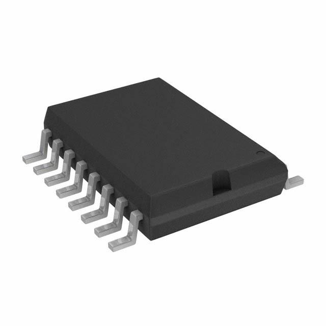
| 供应商器件封装 | 14-SOP |
| 其它名称 | FAN7382M1XCT |
| 包装 | 剪切带 (CT) |
| 单位重量 | 218.300 mg |
| 商标 | Fairchild Semiconductor |
| 安装类型 | 表面贴装 |
| 安装风格 | SMD/SMT |
| 封装 | Reel |
| 封装/外壳 | 14-SOIC(0.154",3.90mm 宽) |
| 封装/箱体 | SOP-14 |
| 工作温度 | -40°C ~ 125°C |
| 工厂包装数量 | 3000 |
| 延迟时间 | 170ns |
| 最大功率耗散 | 1 W |
| 最大工作温度 | + 125 C |
| 最小工作温度 | - 40 C |
| 标准包装 | 1 |
| 激励器数量 | 2 Driver |
| 电压-电源 | 10 V ~ 20 V |
| 电流-峰值 | 350mA |
| 电源电压-最大 | 20 V |
| 电源电压-最小 | 10 V |
| 电源电流 | 0.6 mA |
| 类型 | Half-Bridge Driver |
| 系列 | FAN7382 |
| 输入类型 | 非反相 |
| 输出数 | 2 |
| 输出电压 | +/- 0.3 V |
| 输出电流 | 650 mA |
| 输出端数量 | 2 |
| 配置 | 半桥 |
| 配置数 | 1 |
| 高压侧电压-最大值(自举) | 600V |


- 商务部:美国ITC正式对集成电路等产品启动337调查
- 曝三星4nm工艺存在良率问题 高通将骁龙8 Gen1或转产台积电
- 太阳诱电将投资9.5亿元在常州建新厂生产MLCC 预计2023年完工
- 英特尔发布欧洲新工厂建设计划 深化IDM 2.0 战略
- 台积电先进制程称霸业界 有大客户加持明年业绩稳了
- 达到5530亿美元!SIA预计今年全球半导体销售额将创下新高
- 英特尔拟将自动驾驶子公司Mobileye上市 估值或超500亿美元
- 三星加码芯片和SET,合并消费电子和移动部门,撤换高东真等 CEO
- 三星电子宣布重大人事变动 还合并消费电子和移动部门
- 海关总署:前11个月进口集成电路产品价值2.52万亿元 增长14.8%


PDF Datasheet 数据手册内容提取
Is Now Part of To learn more about ON Semiconductor, please visit our website at www.onsemi.com Please note: As part of the Fairchild Semiconductor integration, some of the Fairchild orderable part numbers will need to change in order to meet ON Semiconductor’s system requirements. Since the ON Semiconductor product management systems do not have the ability to manage part nomenclature that utilizes an underscore (_), the underscore (_) in the Fairchild part numbers will be changed to a dash (-). This document may contain device numbers with an underscore (_). Please check the ON Semiconductor website to verify the updated device numbers. The most current and up-to-date ordering information can be found at www.onsemi.com. Please email any questions regarding the system integration to Fairchild_questions@onsemi.com. ON Semiconductor and the ON Semiconductor logo are trademarks of Semiconductor Components Industries, LLC dba ON Semiconductor or its subsidiaries in the United States and/or other countries. ON Semiconductor owns the rights to a number of patents, trademarks, copyrights, trade secrets, and other intellectual property. A listing of ON Semiconductor’s product/patent coverage may be accessed at www.onsemi.com/site/pdf/Patent-Marking.pdf. ON Semiconductor reserves the right to make changes without further notice to any products herein. ON Semiconductor makes no warranty, representation or guarantee regarding the suitability of its products for any particular purpose, nor does ON Semiconductor assume any liability arising out of the application or use of any product or circuit, and specifically disclaims any and all liability, including without limitation special, consequential or incidental damages. Buyer is responsible for its products and applications using ON Semiconductor products, including compliance with all laws, regulations and safety requirements or standards, regardless of any support or applications information provided by ON Semiconductor. “Typical” parameters which may be provided in ON Semiconductor data sheets and/or specifications can and do vary in different applications and actual performance may vary over time. All operating parameters, including “Typicals” must be validated for each customer application by customer’s technical experts. ON Semiconductor does not convey any license under its patent rights nor the rights of others. ON Semiconductor products are not designed, intended, or authorized for use as a critical component in life support systems or any FDA Class 3 medical devices or medical devices with a same or similar classification in a foreign jurisdiction or any devices intended for implantation in the human body. Should Buyer purchase or use ON Semiconductor products for any such unintended or unauthorized application, Buyer shall indemnify and hold ON Semiconductor and its officers, employees, subsidiaries, affiliates, and distributors harmless against all claims, costs, damages, and expenses, and reasonable attorney fees arising out of, directly or indirectly, any claim of personal injury or death associated with such unintended or unauthorized use, even if such claim alleges that ON Semiconductor was negligent regarding the design or manufacture of the part. ON Semiconductor is an Equal Opportunity/Affirmative Action Employer. This literature is subject to all applicable copyright laws and is not for resale in any manner.
F A N 7 February 2007 3 8 FAN7382 2 H High- and Low-Side Gate Driver i g h - a Features Description n d (cid:132) Floating Channels Designed for Bootstrap Operation The FAN7382, a monolithic high and low side gate-drive L o to +600V IC, can drive MOSFETs and IGBTs that operate up to w (cid:132) Typically 350mA/650mA Sourcing/Sinking Current +600V. Fairchild’s high-voltage process and common- -S Driving Capability for Both Channels mode noise canceling technique provides stable opera- i d (cid:132) Common-Mode dv/dt Noise Canceling Circuit tion of the high-side driver under high-dv/dt noise circum- e stances. An advanced level-shift circuit allows high-side G (cid:132) Extended Allowable Negative VS Swing to -9.8V for gate driver operation up to V =-9.8V (typical) for a Signal Propagation at V =V =15V S t CC BS V =15V. The input logic level is compatible with stan- e (cid:132) VCC & VBS Supply Range from 10V to 20V daBrSd TTL-series logic gates. UVLO circuits for both chan- D r (cid:132) UVLO Functions for Both Channels nels prevent malfunction when V or V is lower than i CC BS v (cid:132) TTL Compatible Input Logic Threshold Levels the specified threshold voltage. Output drivers typically e r (cid:132) Matched Propagation Delay Below 50nsec source/sink 350mA/650mA, respectively, which is suit- able for fluorescent lamp ballasts, PDP scan drivers, (cid:132) Output In-phase with Input Signal motor controls, etc. Applications (cid:132) PDP Scan Driver (cid:132) Fluorescent Lamp Ballast 8-SOP 8-DIP 14-SOP (cid:132) SMPS (cid:132) Motor Driver Ordering Information Part Number Package Pb-Free Operating Temperature Range Packing Method FAN7382N 8-DIP Tube FAN7382M(1) Tube 8-SOP FAN7382MX(1) Yes -40°C ~ 125°C Tape & Reel FAN7382M1(1) Tube 14-SOP FAN7382M1X(1) Tape & Reel Note: 1. These devices passed wave soldering test by JESD22A-111. © 2005 Fairchild Semiconductor Corporation www.fairchildsemi.com FAN7382 Rev. 1.0.8
F A Typical Application Circuit N 7 3 8 2 15V 600V H i g h RBOOT DBOOT - a n d L 1 VCC VB 8 ow Q1 R1 -S HIN 2 HIN HO 7 i d CBOOT R2 e LIN 3 LIN VS 6 G C1 R3 Q2 ate 4 COM LO 5 Load D r R4 i v e r FAN7382 Rev.05 Figure 1. Application Circuit for Half-Bridge Internal Block Diagram 8 V B UVLO D R GE IV 7 HO HIN 2 HS(ON/OFF) NERAPULS CANNCOEISLELER RS R Q ER 500K TOE R 6 V S UVLO 1 VCC D R LIN 3 LS(ON/OFF) DELAY IV 5 LO E R 500K 4 COM FAN7382 Rev.04 Figure 2. Functional Block Diagram © 2005 Fairchild Semiconductor Corporation www.fairchildsemi.com FAN7382 Rev. 1.0.8 2
F A Pin Assignments N 7 3 8 2 H FAN7382N FAN7382M1 ig FAN7382M h - a n VCC 1 8 VB VCC 1 14 NC d L o HIN 2 7 HO HIN 2 13 V w B - S i LIN 3 6 V LIN 3 12 HO d S e G COM 4 5 LO NC 4 11 VS a t e NC 5 10 NC D r FAN7382 Rev.05 i v COM 6 9 NC er LO 7 8 NC FAN7382 Rev.01 Figure 3. Pin Configuration (Top View) Pin Definitions Name Description V Low-Side Supply Voltage CC HIN Logic Input for High-Side Gate Driver Output LIN Logic Input for Low-Side Gate Driver Output COM Logic Ground and Low-Side Driver Return LO Low-Side Driver Output V High-Voltage Floating Supply Return S HO High-Side Driver Output V High-Side Floating Supply B © 2005 Fairchild Semiconductor Corporation www.fairchildsemi.com FAN7382 Rev. 1.0.8 3
F A Absolute Maximum Ratings N 7 3 Stresses exceeding the absolute maximum ratings may damage the device. The device may not function or be opera- 8 ble above the recommended operating conditions and stressing the parts to these levels is not recommended. In addi- 2 tion, extended exposure to stresses above the recommended operating conditions may affect device reliability. The H absolute maximum ratings are stress ratings only. ig h Symbol Characteristics Min. Max. Unit - a V High-side offset voltage V -25 V +0.3 n S B B d V High-side floating supply voltage -0.3 625 L B o V High-side floating output voltage HO V -0.3 V +0.3 w HO S B - V Low-side and logic fixed supply voltage -0.3 25 V S CC i d VLO Low-side output voltage LO -0.3 VCC+0.3 e G V Logic input voltage (HIN, LIN) -0.3 V +0.3 IN CC a COM Logic ground VCC-25 VCC+0.3 te D dV /dt Allowable offset voltage slew rate 50 V/ns S r i 8-SOP 0.625 v e P (2)(3)(4) Power dissipation 14-SOP 1.0 W r D 8-DIP 1.2 8-SOP 200 θ Thermal resistance, junction-to-ambient 14-SOP 110 °C/W JA 8-DIP 100 T Junction temperature 150 °C J T Storage temperature 150 °C STG Notes: 2. Mounted on 76.2 x 114.3 x 1.6mm PCB (FR-4 glass epoxy material). 3. Refer to the following standards: JESD51-2: Integral circuits thermal test method environmental conditions - natural convection JESD51-3: Low effective thermal conductivity test board for leaded surface mount packages 4. Do not exceed P under any circumstances. D Recommended Operating Ratings The Recommended Operating Conditions table defines the conditions for actual device operation. Recommended operating conditions are specified to ensure optimal performance to the datasheet specifications. Fairchild does not recommend exceeding them or designing to Absolute Maximum Ratings. Symbol Parameter Min. Max. Unit V High-side floating supply voltage V +10 V +20 B S S V High-side floating supply offset voltage 6-V 600 S CC V High-side (HO) output voltage V V HO S B V V Low-side (LO) output voltage COM V LO CC V Logic input voltage (HIN, LIN) COM V IN CC V Low-side supply voltage 10 20 CC T Ambient temperature -40 125 °C A © 2005 Fairchild Semiconductor Corporation www.fairchildsemi.com FAN7382 Rev. 1.0.8 4
F A Electrical Characteristics N 7 3 V (V , V )=15.0V, T = 25°C, unless otherwise specified. The V and I parameters are referenced to COM. BIAS CC BS A IN IN 8 The V and I parameters are referenced to V and COM and are applicable to the respective outputs HO and LO. 2 O O S H Symbol Characteristics Test Condition Min. Typ. Max. Unit i g V V and V supply under-voltage h CCUV+ CC BS 8.2 9.2 10.0 - V positive going threshold BSUV+ a n V V and V supply under-voltage CCUV- CC BS 7.6 8.7 9.6 V d VBSUV- negative going threshold L o V V supply under-voltage lockout CCUVH CC 0.6 w VBSUVH hysteresis -S I Offset supply leakage current V =V =600V 50 i LK B S d e I Quiescent V supply current V =0V or 5V 45 120 µA QBS BS IN G IQCC Quiescent VCC supply current VIN=0V or 5V 70 180 a t I Operating V supply current f =20kHz,rms value 600 e PBS BS IN µA D I Operating V supply current f =20kHz,rms value 600 PCC CC IN r i V Logic "1" input voltage 2.9 v IH e r V Logic "0" input voltage 0.8 IL V V High-level output voltage, V -V 1.0 OH BIAS O I =20mA O V Low-level output voltage, V 0.6 OL O I Logic "1" input bias current V =5V 10 20 IN+ IN µA I Logic "0" input bias current V =0V 1.0 2.0 IN- IN I Output high short-circuit pulsed current V =0V, V =5V with PW<10µs 250 350 O+ O IN mA I Output low short-circuit pulsed current V =15V, V =0V with PW<10µs 500 650 O- O IN Allowable negative V pin voltage for V S -9.8 -7.0 V S HIN signal propagation to HO Dynamic Electrical Characteristics V (V , V )=15.0V, V =COM, C =1000pF and, T = 25°C, unless otherwise specified. BIAS CC BS S L A Symbol Characteristics Test Condition Min. Typ. Max. Unit t Turn-on propagation delay V =0V 100 170 300 on S t Turn-off propagation delay V =0V or 600V(5) 100 200 300 off S t Turn-on rise time 20 60 140 ns r t Turn-off fall time 30 80 f MT Delay matching, HS & LS turn-on/off 50 Note: 5. This parameter guaranteed by design. © 2005 Fairchild Semiconductor Corporation www.fairchildsemi.com FAN7382 Rev. 1.0.8 5
F A Typical Characteristics N 7 3 8 2 330000 330000 H nsec]nsec] VCVCVCCOCCOOCM=CCMMV=====B0VV00SVBBVVSS nsec]nsec] 227755 VCVCVCCOCCOOCM=CCMMV=====B0VV00SVBB=VV1SS 5==V1155VV igh Delay [Delay [ 225500 CTCTCTALaaLL======2122115n55nn°F°°CFFCC Delay [Delay [ 222225255050 CCCLLL===1n11nnFFF HHiigghh--SSiiddee - and n n n n 220000 gatiogatio 220000 HHiigghh--SSiiddee gatiogatio 117755 LLooww--SSiiddee Low papa papa 115500 - oo oo S n-On Prn-On Pr 115500 LLooww--SSiiddee n-On Prn-On Pr 111102020505 ide G urur 110000 urur 7755 a TT TT t 5500 e 1100 1122 1144 1166 1188 2200 --4400 --2200 00 2200 4400 6600 8800 110000 112200 D SSuuppppllyy VVoollttaaggee [[VV]] TTeemmppeerraattuurree[[°°CC]] r i v Figure 4. Turn-On Propagation Delay vs. Figure 5. Turn-On Propagation Delay vs. Temp. e r Supply Voltage 330000 333000000 nsec]nsec] 228800 VCCOCM=V=VCVCB0CCOOSVCCMM====VV00BBVVSS nsec]nsec]nsec] 222777555 VCVCVCCOCCOOCMCC=MMV=====VVB000SVBBVV=SS 1==5V1155VV y [y [ 226600 C =1nCCFLL==11nnFF y [y [y [ CCCLL===111nnnFFF DelaDela 224400 TAL=25TT°aaC==2255°°CC DelaDelaDela 222555000 L on on 222200 HHiigghh--SSiiddee on on on 222222555 HHHiiiggghhh---SSSiiidddeee atiati 220000 atiatiati gg ggg LLLooowww---SSSiiidddeee aa LLooww--SSiiddee aaa 222000000 pp 118800 ppp oo ooo rr rrr PP 116600 PPP 111777555 Off Off 114400 Off Off Off n-n- n-n-n- 111555000 urur 112200 ururur TT TTT 110000 111222555 1100 1122 1144 1166 1188 2200 ---444000 ---222000 000 222000 444000 666000 888000 111000000 111222000 SSuuppppllyy VVoollttaaggee [[VV]] TTTeeemmmpppeeerrraaatttuuurrreee [[[°°°CCC]]] Figure 6. Turn-Off Propagation Delay vs. Figure 7. Turn-Off Propagation Delay vs. Temp. Supply Voltage 6644 8800 e [nsec]e [nsec] 566566802802 VCCTACLO==CM=21VCCTVCCTV5n=aaCCLLOO°BF0C==S==CCVMM2211==55==nnVV°°00FFCCBBVVSS e [nsec]e [nsec] 56677566775050550505 VCCVCCVCCCOLCCLLOO=CM===CC1MMV11n=====nnBF0VV00SFFVBB=VV1SS 5==V1155VV mm 5566 mm 5500 LLooww--SSiiddee g Tig Ti 5544 g Tig Ti 4455 nn nn 4400 sisi 5522 LLooww--SSiiddee sisi 3355 HHiigghh--SSiiddee n-On Rin-On Ri 45458080 HHiigghh--SSiiddee n-On Rin-On Ri 223223050050 urur 4466 urur 1155 TT TT 1100 4444 55 4422 00 1100 1111 1122 1133 1144 1155 1166 1177 1188 1199 2200 --4400 --2200 00 2200 4400 6600 8800 110000 112200 SSuuppppllyy VVoollttaaggee [[VV]] TTeemmppeerraattuurree [[°°CC]] Figure 8. Turn-On Rising Time vs. Supply Voltage Figure 9. Turn-On Rising Time vs. Temp. © 2005 Fairchild Semiconductor Corporation www.fairchildsemi.com FAN7382 Rev. 1.0.8 6
F A Typical Characteristics (Continued) N 7 3 8 2 555000 H ec]ec] 33332424 VCCOCM=V=VCVCB0CCOOSVCCMM====VV00BBVVSS ec]ec]ec] 444555 VCVCVCCOCCOOCMCC=MMV=====B0VV00SVBBVV=1SS 5==V1155VV igh e [nse [ns 3300 CTAL==215nCTCT°FaaLLC====221155nn°°FFCC e [nse [nse [ns 444000 CCCLLL===111nnnFFF - an TimTim 2288 HHiigghh--SSiiddee TimTimTim 333555 HHHiiiggghhh---SSSiiidddeee d g g 2266 g g g L nn nnn 333000 o allialli 2244 alliallialli w n-Off Fn-Off F 22220202 LLooww--SSiiddee n-Off Fn-Off Fn-Off F 222222050505 LLLooowww---SSSiiidddeee -Side TurTur 1188 TurTurTur 111555 G a 1166 111000 te 1100 1111 1122 1133 1144 1155 1166 1177 1188 1199 2200 ---444000 ---222000 000 222000 444000 666000 888000 111000000 111222000 D SSuuppppllyy VVoollttaaggee [[VV]] TTTeeemmmpppeeerrraaatttuuurrreee [[[°°°CCC]]] r i v Figure 10. Turn-Off Falling Time vs. Supply Voltage Figure 11. Turn-Off Falling Time vs. Temp. e r 660000 mA]mA] 555500 VCVCVCCOCCOOCM=CCMMV=====B0VV00SVBBVVSS mA]mA] 444424240000 VCVCVCCOCCOOCM=CCMMV=====B0VV00SVBBVV=SS1 5==V1155VV urrent [urrent [ 445445050050000000 LTLTLTOAaaOO====2==H225HH55O°OOC°°=CC==000VVV Current [Current [ 343480800000 LLLOOO===HHHOOO===000VVV rcing Crcing C 333305050000 HHiigghh--SSiiddee urcing urcing 333346460000 LLooww--SSiiddee HHiigghh--SSiiddee ouou LLooww--SSiiddee SoSo Output SOutput S 122122505505000000 Output Output 333302020000 228800 110000 1100 1122 1144 1166 1188 2200 --4400 --2200 00 2200 4400 6600 8800 110000 112200 SSuuppppllyy VVoollttaaggee [[VV]] TTeemmppeerraattuurree [[°°CC]] Figure 12. Output Sourcing Current vs. Supply Figure 13. Output Sourcing Current vs. Temp Voltage 990000 885500 mA]mA] 880000 VCVCVCCOCCOOCM=CCMMV=====B0VV00SVBBVVSS mA]mA] 880000 VCVCVCCOCCOOCM=CCMMV=====B0VV00SVBBVV=1SS 5==V1155VV nt [nt [ LLTLTOaaOO=====V22VVC55CCC°°,CCCC H,, OHH=OOV==BVVBB nt [nt [ 775500 LLLOOO===VVVCCCC,CC H,, OHH=OOV==BVVBB CurreCurre 770000 TA=25°CLLooww--SSiiddee HHiigghh--SSiiddee CurreCurre 770000 g g 660000 g g HHiigghh--SSiiddee nn nn kiki kiki 665500 nn nn SiSi 550000 SiSi LLooww--SSiiddee ut ut ut ut 660000 pp pp OutOut 440000 OutOut 555500 330000 550000 1100 1122 1144 1166 1188 2200 --4400 --2200 00 2200 4400 6600 8800 110000 112200 SSuuppppllyy VVoollttaaggee [[VV]] TTeemmppeerraattuurree [[°°CC]] Figure 14. Output Sinking Current vs. Supply Voltage Figure 15. Output Sinking Current vs. Temp. © 2005 Fairchild Semiconductor Corporation www.fairchildsemi.com FAN7382 Rev. 1.0.8 7
F A Typical Characteristics (Continued) N 7 3 8 2 Allowable Negative V VoltageAllowable Negative VS VoltageAllowable Negative VS VoltageSor Signal Propagation to High-Side [V]for Signal Propagatioto High-Side [V]for Signal Propagatioto High-Side [V] ----------1111111111------8648648642086420 VCTACO=CM=2V5=VCTVCT°B0CaaCCSOOV==CCMM22==55==VV°°00CCBBVVSS Allowable Negative V VoltageAllowable Negative VS VoltageAllowable Negative VS VoltageAllowable Negative VS VoltageSor Signal Propagation to High-Side [V]for Signal Propagation to High-Side [V]for Signal Propagation to High-Side [V]for Signal Propagation to High-Side [V] ---------111111111---------------999999999999999000000000........................864208642086420420420420 VCVCVCCOCCOOCMCCMM=V=====VVB000SBBVVV=SS 1==511V55VV High- and Low-Side Gate f 1100 1122 1144 1166 1188 2200 f ---444000 ---222000 000 222000 444000 666000 888000 111000000 111222000 D SSuuppppllyy VVoollttaaggee [[VV]] TTTeeemmmpppeeerrraaatttuuurrreee [[[°°°CCC]]] r i v Figure 16. Allowable Negative VS Voltage for Signal Figure 17. Allowable Negative VS Voltage for Signal e r Propagation to High Side vs. Supply Voltage Propagation to High Side vs. Temp. 110000 9955 VCVCVCBOBBSOOM=SSMM1===5==011V00V55VVVV 9900 VCVCVCCOCCCOOM=CCMMV===B0==VVSV00=BBVV1SS 5==V1155VV 8800 HHHINIINN===LLLINIINN===0V00VV 8855 HHIINN==LLIINN==00VV TTaa==2255°°CC HIN=LIN=0V T =25°C 8800 A uA]uA]A] 6600 A]uA]uA] 7755 QCC [QCC [ [μQCC4400 [μQCC [QCC [QCC 67675050 III III 6600 2200 5555 5500 00 4455 00 55 1100 1155 2200 --4400 --2200 00 2200 4400 6600 8800 110000 112200 SSuuppppllyy VVoollttaaggee [[VV]] TTeemmppeerraattuurree [[°°CC]] Figure 18. I vs. Supply Voltage Figure 19. I vs. Temp. QCC QCC 8800 7700 VCVCVCCOCCOOCM=CCMM1===5==011V00V55VVVV 55550202 VCCOCVCVCM=CCOO1=CC5MM0V==V==110055VVVV 6600 HHTHTINaaIINN=====22L55LLIN°°IINNCC===0V00VV 4488 HINHH=IINNLI==NLL=II0NNV==00VV T =25°C A]A] 5500 A A]A] 4466 I [A]μIQBS [uIQBS [uQBS 34340000 I [A]μIQBS [uIQBS [uQBS 44442424 4400 2200 3388 1100 3366 00 00 55 1100 1155 2200 --4400 --2200 00 2200 4400 6600 8800 110000 112200 SSuuppppllyy VVoollttaaggee [[VV]] TTeemmppeerraattuurree [[°°CC]] Figure 20. I vs. Supply Voltage Figure 21. I vs. Temp. QBS QBS © 2005 Fairchild Semiconductor Corporation www.fairchildsemi.com FAN7382 Rev. 1.0.8 8
F A Typical Characteristics (Continued) N 7 3 8 2 00..77 00..6600 H VCCVV=CCVCCB==SVVBBSS VVVCCCC=CCV==BVVSBB=1SS5==V1155VV ig COCCMOO=MM0V==00VV 00..5555 CCCOOOMMM===000VVV h 00..66 HHIINN==LLIINN==55VV HHIINN==LLIINN==55VV - HINIILL===L22IN00mm=5AAV 00..5500 HIILLIN===22L00ImmNAA=5V a IL=TT2aa0==m22A55°°CC IL=20mA nd V [V]VOH [V]VOH [V]OH0000....4545 HHiigghh--SSiiddTeeA=25°C V [V]VOH [V]VOH [V]OH 0000....44440505 LLooww--SSiiddee HHiigghh--SSiiddee Low- S LLooww--SSiiddee 00..3355 id 00..33 e 00..3300 G a 00..22 00..2255 te 1100 1122 1144 1166 1188 2200 --4400 --2200 00 2200 4400 6600 8800 110000 112200 D SSuuppppllyy VVoollttaaggee [[VV]] TTeemmppeerraattuurree [[°°CC]] r i v Figure 22. High-Level Output Voltage vs. Figure 23. High-Level Output Voltage vs. Temp. e r Supply Voltage 00..1188 V VV=CCVCC==VVBBSS 00..2222 VVVCCCC=CCV==BVVSBB=1SS5==V1155VV CCOCCCMOO=MMB0SV==00VV CCCOOOMMM===000VVV 00..1177 HINHIHILL=II==NNL22I==N00LLmm=IINN0AAV==00VV 00..2200 HIHIHILL=INII==2NN=220==L00mLLmmINIIANNAA===000VVV IL=TT20aam==22A55°°CC 00..1188 L VOL [V]VOL [V]V [V]OL 0000....11115656 THHA=iigg2hh5°--CSSiiddee VOL [V]VOL [V]V [V]OL 00..1166 HHiigghh--SSiiddee LLooww--SSiiddee 00..1144 00..1144 LLooww--SSiiddee 00..1122 00..1133 00..1100 00..1122 1100 1122 1144 1166 1188 2200 --4400 --2200 00 2200 4400 6600 8800 110000 112200 SSuuppppllyy VVoollttaaggee [[VV]] TTeemmppeerraattuurree [[°°CC]] Figure 24. Low-Level Output Voltage vs. Figure 25. Low-Level Output Voltage vs. Temp. Supply Voltage 4400 1166 VVVCCCC=V==VVBBSS HHIINN==LLIINN==55VV 3355 CCCCOOOCMMM===B000SVVV 1144 IINN==VVCCCC oorr IINN==00VV 3300 ITTNaa===V22C55C°° CCor IN=0V T =25°C 1122 uA]uA]A] 2255 A IINN++ A]A]A] LLIINN N+/IN-[N+/IN-[+/IN- [μ 12125050 IN+ [uIN+ [uIN+ [μ 1100 HHIINN IIN 88 I 1100 66 55 IINN-- 00 44 00 55 1100 1155 2200 --4400 --2200 00 2200 4400 6600 8800 110000 112200 SSuuppppllyy VVoollttaaggee [[VV]] TTeemmppeerraattuurree [[°°CC]] Figure 26. Input Bias Current vs. Supply Voltage Figure 27. Input Bias Current vs. Temp. © 2005 Fairchild Semiconductor Corporation www.fairchildsemi.com FAN7382 Rev. 1.0.8 9
F A Typical Characteristics (Continued) N 7 3 8 2 1100..00 1100..00 H i 99..88 99..88 g h 99..66 99..66 - CCUV+/VCCUV-[V]CCUV+/VCCUV-[V]V/V [V]CCUV+CCUV+ 8899988999..........6802468024 VVVVVCCCCVCCCCCCCUCUUUUVUVV+VVV-++-- BSUV+/VBSUV-[V]BSUV+/VBSUV-[V]V/V [V]SBUV+SBUV+ 8899988999..........6802468024 VVVBBVVSVSSBBBSUUUSSBVUVV+UUV++VV- -- and Low-Sid VV 88..44 VV 88..44 e G 88..22 88..22 a t 88..00 88..00 e --4400 --2200 00 2200 4400 6600 8800 110000 112200 --4400 --2200 00 2200 4400 6600 8800 110000 112200 D TTeemmppeerraattuurree [[°°CC]] TTeemmppeerraattuurree [[°°CC]] r i v Figure 28. VCC UVLO Threshold Voltage vs. Temp. Figure 29. VBS UVLO Threshold Voltage vs. Temp. e r 4545 VVVBBB-t--ottoo-C--CCOOOMMM=6==566055V00VV age [V]age [V] 23332333........80248024 VVVIIHHIH(( (LLLIIINNN))) VCVCVCCOCCOOCM=CCMMV=====B0VV00SVBB=VV1SS5==V1155VV oltolt 22..66 VV 22..44 d d 22..22 VVVIIHHIH (((HHHIIINNN))) ILK [uA]ILK [uA]I [A]μLK 2323 ThresholThreshol 11121112........46804680 VVVIILL(((HHHIINNIVVNV))IILL)IL(( (LLLIINNIN))) c c 11..22 IL gigi 11..00 oo 00..88 11 LL put put 0000....4646 nn 00..22 00 II 00..00 --4400 --2200 00 2200 4400 6600 8800 110000 112200 --4400 --2200 00 2200 4400 6600 8800 110000 112200 TTeemmppeerraattuurree [[°°CC]] TTeemmppeerraattuurree [[°°CC]] Figure 30. V to COM Leakage Current vs. Temp. Figure 31. Input Logic Threshold Voltage vs. Temp. B © 2005 Fairchild Semiconductor Corporation www.fairchildsemi.com FAN7382 Rev. 1.0.8 10
F A Typical Characteristics (Continued) N 7 3 8 2 15V 15V H i g h 1 VCC VB 8 - a 100nF 10uF 10uF 100nF n 4 COM VS 6 d HIN 1nF L LIN o HIN 2 HIN HO 7 w - S LIN 3 LIN LO 5 i 1nF HO de LO G FAN7382 Rev.05 FAN7382 Rev.03 a t Figure 32. Switching Time Test Circuit Figure 33. Input / Output Timing Diagram e D r i v e r t : Turn-on Delay Time on HIN 50% ttof f: T: uTrunr-no-no fRf Diseel aTyim Teime 50% HIN 50% 50% LIN trf : Turn-off Fall Time LIN ton tr toff tf LO MT HO t off-H 10% toff-L t 90% 90% ton-L on-H 90% HO LO HO LO 10% 10% MT FAN7382 Rev.03 FAN7382 Rev.03 Figure 34. Switching Time Waveform Definition Figure 35. Delay Matching Waveform Definition © 2005 Fairchild Semiconductor Corporation www.fairchildsemi.com FAN7382 Rev. 1.0.8 11
9.83 9.00 8 5 6.670 6.096 1 4 TOP VIEW 8.255 7.610 1.65 (0.56) 7.62 1.27 3.683 5.08 MAX 3.200 3.60 0.33 MIN 3.00 0.356 15° 0.560 0.200 0° 2.54 0.355 9.957 7.62 7.870 FRONT VIEW SIDE VIEW NOTES: A. CONFORMS TO JEDEC MS-001, VARIATION BA B. ALL DIMENSIONS ARE IN MILLIMETERS C. DIMENSIONS ARE EXCLUSIVE OF BURRS, MOLD FLASH, AND TIE BAR EXTRUSIONS D. DIMENSIONS AND TOLERANCES PER ASME Y14.5M-2009 E. DRAWING FILENAME: MKT-N08Frev3
5.12 C A 4.72 0.35 8 5 B 1.75 0.65 6.30 4.15 5.70 3.75 5.60 1.27 1 4 1.27 PIN #1 ID 0.25 M C B A LAND PATTERN RECOMMENDATION TOP VIEW 1.85 1.75 B 0.25 1.35 C 1.25 C 0.15 C 0.51 0.25 (8X) 0.31 OPTION A OPTION B 0.10 BEVEL EDGE NON-BEVEL EDGE 0.10 C SIDE VIEW FRONT VIEW NOTES: UNLESS OTHERWISED SPECIFIED GAGE PLANE BEVEL R0.10 A. THIS PACKAGE CONFORMS TO JEDEC MS-012 VARIATION A EXCEPT WHERE NOTED. 0.25 B. ALL DIMENSIONS ARE IN MILLIMETERS C OUT OF JEDEC STANDARD VALUE 8° 4° D. DIMENSIONS ARE EXCLUSIVE OF BURRS, 0.80 MOLD FLASH AND TIE BAR EXTRUSIONS. SEATING 0.30 E. LAND PATTERN AS PER IPC PLANE 1.04 SOIC127P600X175-8M F. DRAWING FILENAME: MKT-M08Brev2 DETAIL "B" SCALE 2:1
8.76 A 8.36 7.62 0.65 B 1.70 14 8 1.27 4.20 5.60 6.00 3.75 1 7 PIN #1 ID 1.27 0.27 TOP VIEW E 1.65 CHAMFER OPTIONAL 1.25 1.80 MAX C A 0.25 E 0.51 0.30 0.05 E 0.36 0.15 0.10 C 0.20 M C A B ALL LEAD TIPS END VIEW SIDE VIEW GGAAUUGGEE PPLLAANNEE 00..3366 NOTES: UNLESS OTHERWISE SPECIFIED SSEEAATTIINNGG PPLLAANNEE 00~~55°° A. THIS PACKAGE REFERENCE TO JEDEC MS-012 VARIATION AB. B. ALL DIMENSIONS ARE IN MILLIMETERS. C. DIMENSIONS ARE EXCLUSIVE OF BURRS, 00..9900 MOLD FLASH AND TIE BAR EXTRUSIONS. 00..4455 D. DIMENSIONS AND TOLERANCES AS PER ASME 11..0044 Y14.5-1994. E OUT OF JEDEC STANDARD VALUE. DETAIL "A" F. LAND PATTERN STANDARD: SOIC127P600X145-14M. SCALE 2:1 G. FILE NAME: MKT-M14C REV2
ON Semiconductor and are trademarks of Semiconductor Components Industries, LLC dba ON Semiconductor or its subsidiaries in the United States and/or other countries. ON Semiconductor owns the rights to a number of patents, trademarks, copyrights, trade secrets, and other intellectual property. A listing of ON Semiconductor’s product/patent coverage may be accessed at www.onsemi.com/site/pdf/Patent−Marking.pdf. ON Semiconductor reserves the right to make changes without further notice to any products herein. ON Semiconductor makes no warranty, representation or guarantee regarding the suitability of its products for any particular purpose, nor does ON Semiconductor assume any liability arising out of the application or use of any product or circuit, and specifically disclaims any and all liability, including without limitation special, consequential or incidental damages. Buyer is responsible for its products and applications using ON Semiconductor products, including compliance with all laws, regulations and safety requirements or standards, regardless of any support or applications information provided by ON Semiconductor. “Typical” parameters which may be provided in ON Semiconductor data sheets and/or specifications can and do vary in different applications and actual performance may vary over time. All operating parameters, including “Typicals” must be validated for each customer application by customer’s technical experts. ON Semiconductor does not convey any license under its patent rights nor the rights of others. ON Semiconductor products are not designed, intended, or authorized for use as a critical component in life support systems or any FDA Class 3 medical devices or medical devices with a same or similar classification in a foreign jurisdiction or any devices intended for implantation in the human body. Should Buyer purchase or use ON Semiconductor products for any such unintended or unauthorized application, Buyer shall indemnify and hold ON Semiconductor and its officers, employees, subsidiaries, affiliates, and distributors harmless against all claims, costs, damages, and expenses, and reasonable attorney fees arising out of, directly or indirectly, any claim of personal injury or death associated with such unintended or unauthorized use, even if such claim alleges that ON Semiconductor was negligent regarding the design or manufacture of the part. ON Semiconductor is an Equal Opportunity/Affirmative Action Employer. This literature is subject to all applicable copyright laws and is not for resale in any manner. PUBLICATION ORDERING INFORMATION LITERATURE FULFILLMENT: N. American Technical Support: 800−282−9855 Toll Free ON Semiconductor Website: www.onsemi.com Literature Distribution Center for ON Semiconductor USA/Canada 19521 E. 32nd Pkwy, Aurora, Colorado 80011 USA Europe, Middle East and Africa Technical Support: Order Literature: http://www.onsemi.com/orderlit Phone: 303−675−2175 or 800−344−3860 Toll Free USA/Canada Phone: 421 33 790 2910 Fax: 303−675−2176 or 800−344−3867 Toll Free USA/Canada Japan Customer Focus Center For additional information, please contact your local Email: orderlit@onsemi.com Phone: 81−3−5817−1050 Sales Representative © Semiconductor Components Industries, LLC www.onsemi.com www.onsemi.com 1
Mouser Electronics Authorized Distributor Click to View Pricing, Inventory, Delivery & Lifecycle Information: O N Semiconductor: FAN7382M FAN7382MX FAN7382N FAN7382M1X