ICGOO在线商城 > 集成电路(IC) > PMIC - 栅极驱动器 > UCC27517DBVT
 Datasheet下载
- 型号: UCC27517DBVT
- 制造商: Texas Instruments
- 库位|库存: xxxx|xxxx
- 要求:
| 数量阶梯 | 香港交货 | 国内含税 |
| +xxxx | $xxxx | ¥xxxx |
查看当月历史价格
查看今年历史价格
UCC27517DBVT产品简介:
ICGOO电子元器件商城为您提供UCC27517DBVT由Texas Instruments设计生产,在icgoo商城现货销售,并且可以通过原厂、代理商等渠道进行代购。 UCC27517DBVT价格参考¥12.60-¥15.75。Texas InstrumentsUCC27517DBVT封装/规格:PMIC - 栅极驱动器, Low-Side Gate Driver IC Inverting, Non-Inverting SOT-23-5。您可以下载UCC27517DBVT参考资料、Datasheet数据手册功能说明书,资料中有UCC27517DBVT 详细功能的应用电路图电压和使用方法及教程。
Texas Instruments(德州仪器)的UCC27517DBVT是一款高性能的PMIC(电源管理集成电路)栅极驱动器,广泛应用于需要高效、快速响应和高可靠性的电力电子系统中。该器件的主要应用场景包括但不限于以下几种:

1. 工业电机控制:在工业自动化和电机控制系统中,UCC27517DBVT可以用于驱动功率MOSFET或IGBT,提供高效的开关控制,确保电机运行的稳定性和效率。其快速的开关速度和低延迟特性有助于提高系统的动态响应能力。

2. 太阳能逆变器:在光伏逆变器中,UCC27517DBVT用于驱动功率器件,实现直流到交流的转换。其高效率和低功耗特性有助于提升逆变器的整体性能,减少能量损失,延长设备寿命。

3. 电动汽车(EV)和混合动力汽车(HEV):在电动汽车和混合动力汽车的电动驱动系统中,UCC27517DBVT可以用于驱动电机控制器中的功率器件,提供高效的开关控制,确保车辆的动力传输和能量回收系统的高效运行。

4. 不间断电源(UPS):在UPS系统中,UCC27517DBVT用于驱动逆变器和电池充电器中的功率器件,确保在市电中断时能够迅速切换到备用电源,保障关键负载的持续供电。

5. 通信电源系统:在通信基站和数据中心的电源管理系统中,UCC27517DBVT可以用于驱动功率转换模块中的MOSFET或IGBT,提供高效、可靠的电源转换,确保通信设备的稳定运行。

6. 消费类电子产品:在一些高端消费类电子产品中,如智能家电、笔记本电脑等,UCC27517DBVT也可以用于驱动电源模块中的功率器件,提供高效、紧凑的电源解决方案。

总之,UCC27517DBVT凭借其卓越的性能和可靠性,在各种电力电子应用中发挥着重要作用,特别是在需要高效能、快速响应和高可靠性的场景下表现尤为突出。
| 参数 | 数值 |
| 产品目录 | 集成电路 (IC)半导体 |
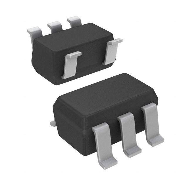
| 描述 | IC GATE DVR LOW SIDE 1CH SOT23-5门驱动器 4A/4A Sgl Ch Hi-Spd Lo-side Gate Driver |
| 产品分类 | PMIC - MOSFET,电桥驱动器 - 外部开关集成电路 - IC |
| 品牌 | Texas Instruments |
| 产品手册 | |
| 产品图片 |
|
| rohs | 符合RoHS无铅 / 符合限制有害物质指令(RoHS)规范要求 |
| 产品系列 | 电源管理 IC,门驱动器,Texas Instruments UCC27517DBVT- |
| 数据手册 | |
| 产品型号 | UCC27517DBVT |
| PCN组件/产地 | |
| 上升时间 | 9 ns |
| 下降时间 | 7 ns |
| 产品 | MOSFET Gate Drivers |
| 产品种类 | 门驱动器 |
| 供应商器件封装 | SOT-23-5 |
| 其它名称 | 296-30370-6 |
| 包装 | Digi-Reel® |
| 商标 | Texas Instruments |
| 安装类型 | 表面贴装 |
| 安装风格 | SMD/SMT |
| 封装 | Reel |
| 封装/外壳 | SC-74A,SOT-753 |
| 封装/箱体 | SOT-23-5 |
| 工作温度 | -40°C ~ 140°C |
| 工厂包装数量 | 250 |
| 延迟时间 | 13ns |
| 最大工作温度 | + 140 C |
| 最小工作温度 | - 40 C |
| 标准包装 | 1 |
| 电压-电源 | 4.5 V ~ 18 V |
| 电流-峰值 | 4A |
| 电源电压-最大 | 18 V |
| 电源电压-最小 | 4.5 V |
| 类型 | High or Low Side MOSFET Drivers |
| 系列 | UCC27517 |
| 输入类型 | 反相和非反相 |
| 输出数 | 1 |
| 输出电流 | 4 A |
| 配置 | 低端 |
| 配置数 | 1 |
| 高压侧电压-最大值(自举) | - |


- 商务部:美国ITC正式对集成电路等产品启动337调查
- 曝三星4nm工艺存在良率问题 高通将骁龙8 Gen1或转产台积电
- 太阳诱电将投资9.5亿元在常州建新厂生产MLCC 预计2023年完工
- 英特尔发布欧洲新工厂建设计划 深化IDM 2.0 战略
- 台积电先进制程称霸业界 有大客户加持明年业绩稳了
- 达到5530亿美元!SIA预计今年全球半导体销售额将创下新高
- 英特尔拟将自动驾驶子公司Mobileye上市 估值或超500亿美元
- 三星加码芯片和SET,合并消费电子和移动部门,撤换高东真等 CEO
- 三星电子宣布重大人事变动 还合并消费电子和移动部门
- 海关总署:前11个月进口集成电路产品价值2.52万亿元 增长14.8%


PDF Datasheet 数据手册内容提取
Product Sample & Technical Tools & Support & Folder Buy Documents Software Community UCC27516,UCC27517 SLUSAY4D–MARCH2012–REVISEDDECEMBER2014 UCC2751x Single-Channel, High-Speed, Low-Side Gate Driver (With 4-A Peak Source and 4-A Peak Sink) 1 Features 2 Applications • Low-CostGate-DriverDeviceOfferingSuperior • Switched-ModePowerSupplies 1 ReplacementofNPNandPNPDiscreteSolutions • DC-DCConverters • 4-APeak-Sourceand4-APeak-SinkSymmetrical • CompanionGate-DriverDevicesforDigital-Power Drive Controllers • FastPropagationDelays(13-nsTypical) • SolarPower,MotorControl,UPS • FastRiseandFallTimes(9-nsand7-nsTypical) • GateDriverforEmergingWideBand-GapPower • 4.5to18-VSingle-SupplyRange Devices(suchasGaN) • OutputsHeldLowDuringVDDUVLO(Ensures 3 Description Glitch-FreeOperationatPowerUpandPower Down) The UCC27516 and UCC27517 single-channel, high- speed, low-side gate driver devices can effectively • TTLandCMOSCompatibleInput-LogicThreshold drive MOSFET and IGBT power switches. Using a (IndependentofSupplyVoltage) design that inherently minimizes shoot-through • Hysteretic-LogicThresholdsforHigh-Noise current, UCC27516 and UCC27517 can source and Immunity sink high peak-current pulses into capacitive loads • DualInputDesign(ChoiceofanInverting(IN– offeringrail-to-raildrivecapabilityandextremelysmall pin)orNoninverting(IN+Pin)Driver propagationdelay,typically13ns. Configuration) The UCC27516 and UCC27517 provides 4-A source, – UnusedInputPinCanBeUsedforEnableor 4-A sink (symmetrical drive) peak-drive current DisableFunction capabilityatVDD=12V. • OutputHeldLowWhenInputPinsAreFloating DeviceInformation(1) • InputPinAbsoluteMaximumVoltageLevelsNot PARTNUMBER PACKAGE BODYSIZE(NOM) RestrictedbyVDDPinBiasSupplyVoltage UCC27516 SON(6) 3.00mm×3.00mm • OperatingTemperatureRangeof–40°Cto140°C UCC27517 SOT-23(5) 2.90mm×1.60mm • 5-PinDBV(SOT-23)and6-PinDRS(3-mm× (1) For all available packages, see the orderable addendum at 3-mmWSONWithExposedThermalPad) theendofthedatasheet. PackageOptions TypicalApplicationDiagrams Non-InvertingInput InvertingInput Q1 Q1 UCC27517 UCC27517 4.5Vto18V R1 4.5Vto18V R1 V+ 1 VDD OUT 5 V+ 1 VDD OUT 5 C1 C1 2 GND 2 GND IN+ 3 IN+ IN- 4 3 IN+ IN- 4 VIN- 1 An IMPORTANT NOTICE at the end of this data sheet addresses availability, warranty, changes, use in safety-critical applications, intellectualpropertymattersandotherimportantdisclaimers.PRODUCTIONDATA.
UCC27516,UCC27517 SLUSAY4D–MARCH2012–REVISEDDECEMBER2014 www.ti.com Table of Contents 1 Features.................................................................. 1 9.3 FeatureDescription.................................................13 2 Applications........................................................... 1 9.4 DeviceFunctionalModes........................................16 3 Description............................................................. 1 10 ApplicationandImplementation........................ 17 4 RevisionHistory..................................................... 2 10.1 ApplicationInformation..........................................17 10.2 TypicalApplication................................................17 5 Description(continued)......................................... 3 11 PowerSupplyRecommendations..................... 21 6 DeviceComparisonTable..................................... 3 12 Layout................................................................... 21 7 PinConfigurationandFunctions......................... 4 12.1 LayoutGuidelines.................................................21 8 Specifications......................................................... 5 12.2 LayoutExample....................................................22 8.1 AbsoluteMaximumRatings......................................5 12.3 ThermalConsiderations........................................23 8.2 ESDRatings ............................................................5 12.4 PowerDissipation.................................................24 8.3 RecommendedOperatingConditions.......................5 13 DeviceandDocumentationSupport................. 26 8.4 ThermalInformation..................................................5 13.1 RelatedLinks........................................................26 8.5 ElectricalCharacteristics...........................................6 13.2 Trademarks...........................................................26 8.6 SwitchingCharacteristics..........................................7 13.3 ElectrostaticDischargeCaution............................26 8.7 TypicalCharacteristics..............................................9 13.4 Glossary................................................................26 9 DetailedDescription............................................ 12 14 Mechanical,Packaging,andOrderable 9.1 Overview.................................................................12 Information........................................................... 26 9.2 FunctionalBlockDiagrams.....................................13 4 Revision History NOTE:Pagenumbersforpreviousrevisionsmaydifferfrompagenumbersinthecurrentversion. ChangesfromRevisionC(May2013)toRevisionD Page • AddedPinConfigurationandFunctionssection,ESDRatingstable,FeatureDescriptionsection,DeviceFunctional Modes,ApplicationandImplementationsection,PowerSupplyRecommendationssection,Layoutsection,Device andDocumentationSupportsection,andMechanical,Packaging,andOrderableInformationsection .............................. 1 ChangesfromRevisionB(June2012)toRevisionC Page • Added0.5tobeginningofP equationinPowerDissipationsection ............................................................................... 25 SW ChangesfromRevisionA(March2012)toRevisionB Page • AddedUCC27516device....................................................................................................................................................... 1 • AddedGND,grounddefinition................................................................................................................................................ 4 • AddedDCandrepetitivepulseratestoOUTvoltage............................................................................................................ 5 • Addednote5.......................................................................................................................................................................... 5 • ChangedHumanBodyModelmaxvaluefrom2000Vto400V............................................................................................ 5 • ChangedChargedDeviceModelmaxvaluefrom500Vto100V........................................................................................ 5 • AddedUCC27516blockdiagram......................................................................................................................................... 13 • AddedPCBlayoutbullet....................................................................................................................................................... 22 • AddedThermalInformationdescription................................................................................................................................ 23 2 SubmitDocumentationFeedback Copyright©2012–2014,TexasInstrumentsIncorporated ProductFolderLinks:UCC27516 UCC27517
UCC27516,UCC27517 www.ti.com SLUSAY4D–MARCH2012–REVISEDDECEMBER2014 5 Description (continued) The UCC27516 and UCC27517 are designed to operate over a wide VDD range of 4.5 to 18 V and wide temperature range of –40°C to 140°C. Internal undervoltage lockout (UVLO) circuitry on the VDD pin holds outputlowoutsideVDDoperatingrange.Thecapabilitytooperateatlowvoltagelevelssuchasbelow5V,along with best-in-class switching characteristics, is especially suited for driving emerging wide band-gap power- switchingdevicessuchasGaNpowersemiconductordevices. The UCC27516 and UCC27517 devices feature a dual-input design which offers flexibility of implementing both inverting (IN– pin) and noninverting (IN+ pin) configurations with the same device. Either the IN+ or IN- pin can be used to control the state of the driver output. The unused input pin can be used for enable and disable function. For safety purpose, internal pullup and pulldown resistors on the input pins ensure that outputs are held low when input pins are in floating condition. Hence the unused input pin is not left floating and must be properly biasedtoensurethatdriveroutputisinenabledfornormaloperation. The input pin threshold of the UCC27516 and UCC27517 devices are based on TTL and CMOS compatible low- voltage logic which is fixed and independent of the VDD supply voltage. Wide hysteresis between the high and lowthresholdsoffersexcellentnoiseimmunity. 6 Device Comparison Table The UCC2751x family of gate-driver products (Table 1) represent TI’s latest generation of single-channel low- side high-speed gate-driver devices featuring high-source/sink current capability, industry best-in-class switching characteristicsandahostofotherfeatures(Table2),allofwhichcombinetoensureefficient,robust,andreliable operationinhigh-frequencyswitchingpowercircuits. Table1.UCC2751xProductFamilySummary PEAKCURRENT PARTNUMBER PACKAGE INPUTTHRESHOLDLOGIC (SOURCE/SINK) UCC27516DRS 3mm×3mmWSON,6pin 4-A/8-A UCC27511DBV SOT-23,6pin (SymmetricalDrive) CMOS/TTL-Compatible (lowvoltage,independentofVDD UCC27516DRS 3mm×3mmWSON,6pin biasvoltage) UCC27517DBV SOT-23,5pin 4-A/4-A UCC27518DBV SOT-23,5pin (SymmetricalDrive) CMOS UCC27519DBV SOT-23,5pin (followsVDDbiasvoltage) Copyright©2012–2014,TexasInstrumentsIncorporated SubmitDocumentationFeedback 3 ProductFolderLinks:UCC27516 UCC27517
UCC27516,UCC27517 SLUSAY4D–MARCH2012–REVISEDDECEMBER2014 www.ti.com 7 Pin Configuration and Functions 5-Pin UCC27517DBVPackage 6-Pin TopView UCC27516DRS TopView VVDDDD 11 55 OOUUTT IN- 1 6 IN+ GGNNDD 22 IINN++ 33 44 IINN-- GND 2 5 OUT GND 3 4 VDD PinFunctions – UCC27516 PIN I/O DESCRIPTION NO. NAME InvertingInput:Whenthedriverisusedinnoninvertingconfiguration,connectIN-to 1 IN– I GNDinordertoenableoutput,OUTheldLOWifIN-isunbiasedorfloating. Ground:Allsignalsreferencedtothispin.TIrecommendstoconnectpin2andpin3 2,3 GND — onPCBasclosetothedeviceaspossible. 4 VDD I Biassupplyinput. 5 OUT I Sourcing/SinkingCurrentOutputofDriver NoninvertingInput:Whenthedriverisusedininvertingconfiguration,connectIN+to 6 IN+ O VDDinordertoenableoutput,OUTheldLOWifIN+isunbiasedorfloating. PinFunctions – UCC27517 PIN I/O DESCRIPTION NO. NAME 1 VDD I Biassupplyinput. Ground.Allsignalsreferencetothispin.FortheUCC27516,TIrecommendsto 2 GND — connectpin2andpin3onPCBasclosetothedeviceaspossible. Noninvertinginput.Whenthedriverisusedininvertingconfiguration,connectIN+to 3 IN+ I VDDinordertoenableoutput,OUTheldLOWifIN+isunbiasedorfloating Invertinginput.Whenthedriverisusedinnoninvertingconfiguration,connectIN-to 4 IN– I GNDinordertoenableoutput,OUTheldLOWifIN-isunbiasedorfloating 5 OUT O Sourcing/Sinkingcurrentoutputofdriver. 4 SubmitDocumentationFeedback Copyright©2012–2014,TexasInstrumentsIncorporated ProductFolderLinks:UCC27516 UCC27517
UCC27516,UCC27517 www.ti.com SLUSAY4D–MARCH2012–REVISEDDECEMBER2014 8 Specifications 8.1 Absolute Maximum Ratings(1)(2)(3) overoperatingfree-airtemperaturerange(unlessotherwisenoted) MIN MAX UNIT Supplyvoltage VDD –0.3 20 DC –0.3 VDD+0.3 V OUTvoltage Repetitivepulselessthan 200ns(4) –2 VDD+0.3 Outputcontinuouscurrent I (source/sink) 0.3 A OUT_DC Outputpulsedcurrent(0.5µs) I (source/sink) 4 OUT_pulsed IN+,IN-(5) –0.3 20 V Operatingvirtualjunctiontemperature,T –40 150 J Soldering,10sec. 300 Leadtemperature °C Reflow 260 Storagetemperature,T –65 150 stg (1) StressesbeyondthoselistedunderAbsoluteMaximumRatingsmaycausepermanentdamagetothedevice.Thesearestressratings onlyandfunctionaloperationofthedeviceattheseoranyotherconditionsbeyondthoseindicatedunderRecommendedOperating Conditionsisnotimplied.Exposuretoabsolute-maximum-ratedconditionsforextendedperiodsmayaffectdevicereliability. (2) AllvoltagesarewithrespecttoGNDunlessotherwisenoted.Currentsarepositiveinto,negativeoutofthespecifiedterminal.See PackagingSectionofthedatasheetforthermallimitationsandconsiderationsofpackages. (3) Thesedevicesaresensitivetoelectrostaticdischarge;followproperdevice-handlingprocedures. (4) Valuesareverifiedbycharacterizationonbench. (5) MaximumvoltageoninputpinsisnotrestrictedbythevoltageontheVDDpin. 8.2 ESD Ratings VALUE UNIT Humanbodymodel(HBM),perANSI/ESDA/JEDECJS-001(1) ±4000 V(ESD) Electrostaticdischarge Charged-devicemodel(CDM),perJEDECspecificationJESD22- V C101(2) ±1000 (1) JEDECdocumentJEP155statesthat500-VHBMallowssafemanufacturingwithastandardESDcontrolprocess. (2) JEDECdocumentJEP157statesthat250-VCDMallowssafemanufacturingwithastandardESDcontrolprocess. 8.3 Recommended Operating Conditions overoperatingfree-airtemperaturerange(unlessotherwisenoted) MIN NOM MAX UNIT Supplyvoltagerange,VDD 4.5 12 18 V Operatingjunctiontemperaturerange –40 140 °C Inputvoltage,IN+andIN- 0 18 V 8.4 Thermal Information UCC27516 UCC27517 THERMALMETRIC(1) WSON SOT-23 UNIT 6PINS 5PINS R Junction-to-ambientthermalresistance 85.6 217.6 θJA R Junction-to-case(top)thermalresistance 100.1 85.8 θJC(top) R Junction-to-boardthermalresistance 58.6 44.0 θJB °C/W ψ Junction-to-topcharacterizationparameter 7.5 4.0 JT ψ Junction-to-boardcharacterizationparameter 58.7 43.2 JB R Junction-to-case(bottom)thermalresistance 23.7 n/a θJC(bot) (1) Formoreinformationabouttraditionalandnewthermalmetrics,seetheICPackageThermalMetricsapplicationreport,SPRA953. Copyright©2012–2014,TexasInstrumentsIncorporated SubmitDocumentationFeedback 5 ProductFolderLinks:UCC27516 UCC27517
UCC27516,UCC27517 SLUSAY4D–MARCH2012–REVISEDDECEMBER2014 www.ti.com 8.5 Electrical Characteristics VDD=12V,T =T =–40°Cto140°C,1-µFcapacitorfromVDDtoGND.Currentsarepositiveinto,negativeoutofthe A J specifiedpin. PARAMETER TESTCONDITIONS MIN TYP MAX UNIT BIASCURRENTS IN+=VDD,IN-=GND 40 100 160 I Startupcurrent VDD=3.4V IN+=IN-=GNDorIN+=IN-=VDD 25 75 145 µA DD(off) IN+=GND,IN-=VDD 20 60 115 UNDERVOLTAGELOCKOUT(UVLO) T =25°C 3.91 4.20 4.5 A V Supplystartthreshold ON T =–40°Cto140°C 3.70 4.20 4.65 A Minimumoperating V V 3.45 3.9 4.35 OFF voltageaftersupplystart V Supplyvoltagehysteresis 0.2 0.3 0.5 DD_H INPUTS(IN+,IN-) Inputsignalhigh OutputhighforIN+pin, V 2.2 2.4 IN_H threshold OutputlowforIN-pin OutputlowforIN+pin, V V Inputsignallowthreshold 1.0 1.2 IN_L OutputhighforIN-pin V Inputsignalhysteresis 1.0 IN_HYS SOURCE/SINKCURRENT Source/sinkpeak ISRC/SNK current(1) CLOAD=0.22µF,FSW=1kHz ±4 A OUTPUTS(OUT) VDD=12V 50 90 VDD- Highoutputvoltage IOUT=–10mA VOH VDD=4.5V 60 130 I =–10mA OUT mV VDD=12 5 10 I =10mA OUT V Lowoutputvoltage OL VDD=4.5V 6 12 I =10mA OUT VDD=12V 5.0 7.5 Outputpullup IOUT=–10mA ROH resistance(2) VDD=4.5V 5.0 11.0 I =–10mA OUT Ω VDD=12V 0.5 1.0 Outputpulldown IOUT=10mA R OL resistance VDD=4.5V 0.6 1.2 I =10mA OUT (1) EnsuredbyDesign. (2) R representson-resistanceofP-ChannelMOSFETinpullupstructureoftheUCC27516andUCC27517'soutputstage. OH 6 SubmitDocumentationFeedback Copyright©2012–2014,TexasInstrumentsIncorporated ProductFolderLinks:UCC27516 UCC27517
UCC27516,UCC27517 www.ti.com SLUSAY4D–MARCH2012–REVISEDDECEMBER2014 8.6 Switching Characteristics overoperatingfree-airtemperaturerange(unlessotherwisenoted) PARAMETER TESTCONDITIONS MIN TYP MAX UNIT VDD=12V 8 12 C =1.8nF t Risetime(1) LOAD R VDD=4.5V 16 22 C =1.8nF LOAD VDD=12V 7 11 C =1.8nF t Falltime(1) LOAD F VDD=4.5V 7 11 C =1.8nF LOAD ns VDD=12V 4 13 23 5-VinputpulseC =1.8nF t IN+tooutputpropagationdelay(1) LOAD D1 VDD=4.5V 4 15 26 5-VinputpulseC =1.8nF LOAD VDD=12V 4 13 23 C =1.8nF t IN-tooutputpropagationdelay(1) LOAD D2 VDD=4.5V 4 19 30 C =1.8nF LOAD (1) SeetimingdiagramsinFigure1,Figure2,Figure3,andFigure4. HHiigghh IINNPPUUTT ((IINN++ ppiinn)) LLooww HHiigghh IINN--ppiinn LLooww 9900%% OOUUTTPPUUTT 1100%% tt tt tt tt DD11 rr DD11 ff (PWMInputtoIN+Pin(IN–PinTiedtoGND)) Figure1. NoninvertingConfiguration HHiigghh IINNPPUUTT ((IINN--ppiinn)) LLooww HHiigghh IINN++ ppiinn LLooww 9900%% OOUUTTPPUUTT 1100%% tt tt tt tt DD22 ff DD22 rr (PWMInputtoIN-Pin(IN+PinTiedtoVDD)) Figure2. InvertingConfiguration Copyright©2012–2014,TexasInstrumentsIncorporated SubmitDocumentationFeedback 7 ProductFolderLinks:UCC27516 UCC27517
UCC27516,UCC27517 SLUSAY4D–MARCH2012–REVISEDDECEMBER2014 www.ti.com HHiigghh IINNPPUUTT ((IINN--ppiinn)) LLooww HHiigghh EENNAABBLLEE ((IINN++ ppiinn)) LLooww 9900%% OOUUTTPPUUTT 1100%% tt tt tt tt DD11 rr DD11 ff (EnableandDisableSignalAppliedtoIN+Pin,PWMInputtoIN-Pin) Figure3. EnableandDisableFunctionUsingIN+Pin HHiigghh IINNPPUUTT ((IINN++ ppiinn)) LLooww HHiigghh EENNAABBLLEE ((IINN--ppiinn)) LLooww 9900%% OOUUTTPPUUTT 1100%% tt tt tt tt DD22 ff DD22 rr (EnableandDisableSignalAppliedtoIN-Pin,PWMInputtoIN+Pin) Figure4. EnableandDisableFunctionUsingIN-Pin 8 SubmitDocumentationFeedback Copyright©2012–2014,TexasInstrumentsIncorporated ProductFolderLinks:UCC27516 UCC27517
UCC27516,UCC27517 www.ti.com SLUSAY4D–MARCH2012–REVISEDDECEMBER2014 8.7 Typical Characteristics 0.12 4 IN+=Low,IN−=Low 0.11 IN+=High, IN−=Low A) 0.1 3.5 m up Current ( 00..0089 IDD (mA) 3 VDD = 12 V Start 0.07 2.5 fCswLo =ad 5 =0 05 0k0H pzF 0.06 VDD = 3.4 V 0.05 2 −50 0 50 100 150 −50 0 50 100 150 Temperature (°C) Temperature (°C) G001 G013 Figure5.StartupCurrentvsTemperature Figure6.OperatingSupplyCurrentvsTemperature(Output Switching) 0.5 4.6 IN+=Low,IN−=Low UVLO Rising A) IN+=High, IN−=Low UVLO Falling m 4.4 nt ( 0.4 V) Curre hold ( 4.2 pply 0.3 hres g Su LO T 4 n V ati 0.2 U er 3.8 p O VDD = 12 V 0.1 3.6 −50 0 50 100 150 −50 0 50 100 150 Temperature (°C) Temperature (°C) G002 G003 Figure7.SupplyCurrentvsTemperature(OutputInDC Figure8.UVLOThresholdVoltagevsTemperature On/OffCondition) 3.5 8 Turn−On VDD = 12 V RoH Turn−Off CLoad = 1.8 nF ) hreshold (V) 2.53 WUp Resistance ( 67 ut T 2 ull− p P In ut 5 1.5 utp VDD = 12 V O Iout = 10 mA 1 4 −50 0 50 100 150 −50 0 50 100 150 Temperature (°C) Temperature (°C) G014 G004 Figure9.InputThresholdvsTemperature Figure10.OutputPullupResistancevsTemperature Copyright©2012–2014,TexasInstrumentsIncorporated SubmitDocumentationFeedback 9 ProductFolderLinks:UCC27516 UCC27517
UCC27516,UCC27517 SLUSAY4D–MARCH2012–REVISEDDECEMBER2014 www.ti.com Typical Characteristics (continued) 1 8 ROL VDD = 12 V CLoad = 1.8 nF ) We ( 0.8 7 esistanc 0.6 me (ns) 6 wn R se Ti Do Ri − ull 0.4 5 P 0.2 4 −50 0 50 100 150 −50 0 50 100 150 Temperature (°C) Temperature (°C) G000 G000 Figure11.OutputPulldownResistancevsTemperature Figure12.RiseTimevsTemperature 10 20 VDD = 12 V Turn−On CLoad = 1.8 nF Turn−Off 9 s) n e (ns) Delay ( 15 m 8 n all Ti gatio F pa 10 o 7 Pr VDD = 12 V 6 5 −50 0 50 100 150 −50 0 50 100 150 Temperature (°C) Temperature (°C) G000 G006 Figure13.FallTimevsTemperature Figure14.InputToOutputPropagationDelayvs Temperature 20 20 VDD=4.5V 18 VDD=12V 18 16 VDD=15V nt (mA) 1124 elay (ns) 1146 e D Supply Curr 1680 Propagation 1102 4 2 CLoad = 1.8 nF 8 Turn−On Turn−Off 0 6 0 100 200 300 400 500 600 700 0 4 8 12 16 20 Frequency (kHz) Supply Voltage (V) G010 G007 Figure15.OperatingSupplyCurrentvsFrequency Figure16.PropagationDelaysvsSupplyVoltage 10 SubmitDocumentationFeedback Copyright©2012–2014,TexasInstrumentsIncorporated ProductFolderLinks:UCC27516 UCC27517
UCC27516,UCC27517 www.ti.com SLUSAY4D–MARCH2012–REVISEDDECEMBER2014 Typical Characteristics (continued) 20 10 8 me (ns) 15 me (ns) 6 Rise Ti 10 Fall Ti 4 5 2 0 4 8 12 16 20 0 4 8 12 16 20 Supply Voltage (V) Supply Voltage (V) G008 G009 Figure17.RiseTimevsSupplyVoltage Figure18.FallTimevsSupplyVoltage Copyright©2012–2014,TexasInstrumentsIncorporated SubmitDocumentationFeedback 11 ProductFolderLinks:UCC27516 UCC27517
UCC27516,UCC27517 SLUSAY4D–MARCH2012–REVISEDDECEMBER2014 www.ti.com 9 Detailed Description 9.1 Overview The UCC2751x single-channel, high-speed, low-side gate-driver device can effectively drive MOSFET and IGBT power switches. Using a design that inherently minimizes shoot-through current, the UCC2751x device can source and sink high peak-current pulses into capacitive loads, offering rail-to-rail drive capability and extremely small propagation delay of 13 ns (typical). The UCC2751x device provides 4-A source, 4-A sink (symmetrical drive) peak-drive current capability. The UCC27511 device is designed to operate over a wide V range of 4.5 DD to18V,andawidetemperaturerangeof –40°Cto140°C. Internal UVLO circuitry on the V pin holds the output low outside V operating range. The capability to DD DD operate at low voltage levels, such as below 5 V, along with best-in-class switching characteristics, is suited for drivingemergingwideband-gappower-switchingdevicessuchasGaNpower-semiconductordevices. The UCC2751x device features a dual-input design which offers flexibility of implementing both inverting (IN– pin) and noninverting (IN+ pin) configuration with the same device. Either the IN+ or IN– pin can be used to control the state of the driver output. The unused input pin can be used for enable and disable functions. For system robustness, internal pullup and pulldown resistors on the input pins ensure that outputs are held low when the input pins are in floating condition. Therefore the unused input pin is not left floating and must be properly biased to ensure that driver output is in enabled for normal operation. The input pin threshold of the device is based on TTL and CMOS-compatible low-voltage logic which is fixed and independent of the V DD supplyvoltage.Widehysteresisbetweenthehighandlowthresholdsoffersexcellentnoiseimmunity. Table2.UCC2751xFamilyofFeaturesandBenefits FEATURE BENEFIT HighSource/SinkCurrentCapability HighcurrentcapabilityoffersflexibilityinemployingUCC2751x 4A/8A(Asymmetrical)–UCC27511/2 familyofdevicestodriveavarietyofpowerswitchingdevicesat 4A/4A(Symmetrical)–UCC2751x varyingspeeds Best-in-class13-ns(typ)Propagationdelay Extremelylow-pulsetransmissiondistortion ExpandedVDDOperatingrangeof4.5Vto18V Flexibilityinsystemdesign LowVDDoperationensurescompatibilitywithemergingwide- ExpandedOperatingTemperaturerangeof-40°Cto140°C bandgappowerdevicessuchasGaN (SeeElectricalCharacteristicstable) VDDUVLOProtection OutputsareheldlowinUVLOcondition,whichensurespredictable glitch-freeoperationatpowerupandpowerdown Outputsheldlowwheninputpins(INx)infloatingcondition Safetyfeature,especiallyusefulinpassingabnormalconditiontests duringsafetycertification Abilityofinputpins(andenablepininUCC27518/9)tohandle Systemsimplification,especiallyrelatedtoauxiliarybiassupply voltagelevelsnotrestrictedbyVDDpinbiasvoltage architecture SplitoutputstructureinUCC27511(OUTH,OUTL) Allowsindependentoptimizationofturnonandturnoffspeeds Strongsinkcurrent(8A)andlowpulldownimpedance(0.375Ω)in HighimmunitytoCxdV/dtMillerturnonevents UCC27511/2 CMOS/TTLcompatibleinputthresholdlogicwithwidehysteresisin Enhancednoiseimmunity,whileretainingcompatibilitywith UCC27511/2/6/7 microcontrollerlogic-levelinputsignals(3.3V,5V)optimizedfor digitalpower CMOSinputthresholdlogicinUCC27518/9(VIN_H–70%VDD, Wellsuitedforslowinput-voltagesignals,withflexibilitytoprogram VIN_L–30%VDD) delaycircuits(RCD) 12 SubmitDocumentationFeedback Copyright©2012–2014,TexasInstrumentsIncorporated ProductFolderLinks:UCC27516 UCC27517
UCC27516,UCC27517 www.ti.com SLUSAY4D–MARCH2012–REVISEDDECEMBER2014 9.2 Functional Block Diagrams VDD IN+ 6 4 VDD VDD 230kW 200kW IN- 1 5 OUT VDD 3 GND GND 2 UVLO Figure19. UCC27516FunctionalBlockDiagram VDD IN+ 3 1 VDD VDD 230kW 200kW IN- 4 5 OUT VDD GND 2 UVLO Figure20. UCC27517FunctionalBlockDiagram 9.3 Feature Description 9.3.1 VDDandUndervoltageLockout The UCC2751x devices have internal UVLO protection feature on the VDD-pin supply-circuit blocks. Whenever the driver is in UVLO condition (for example when V voltage is less than V during power up and when V DD ON DD voltage is less than V during power down), this circuit holds all outputs LOW, regardless of the status of the OFF inputs. The UVLO is typically 4.2 V with 300-mV typical hysteresis. This hysteresis helps prevent chatter when low V -supply voltages have noise from the power supply and also when there are droops in the VDD-bias DD voltage when the system commences switching and there is a sudden increase in I . The capability to operate DD at low voltage levels such as below 5 V, along with best-in-class switching characteristics, is especially suited for drivingemergingGaNwide-bandgappower-semiconductordevices. For example, at power up, the UCC2751x driver output remains LOW until the V voltage reaches the UVLO DD threshold. The magnitude of the OUT signal rises with V until steady-state V is reached. In the noninverting DD DD operation (PWM signal applied to IN+ pin) shown below, the output remains LOW until the UVLO threshold is reached, and then the output is in-phase with the input. In the inverting operation (PWM signal applied to IN- pin) shownbelowtheoutputremainsLOWuntiltheUVLOthresholdisreached,andthentheoutputisout-phasewith the input. In both cases, the unused input pin must be properly biased to enable the output. Note that in these devices the output turns to high-state only if IN+ pin is high and IN- pin is low after the UVLO threshold is reached. Copyright©2012–2014,TexasInstrumentsIncorporated SubmitDocumentationFeedback 13 ProductFolderLinks:UCC27516 UCC27517
UCC27516,UCC27517 SLUSAY4D–MARCH2012–REVISEDDECEMBER2014 www.ti.com Feature Description (continued) Because the driver draws current from the VDD pin to bias all internal circuits, for the best high-speed circuit performance, two VDD bypass capacitors are recommended to prevent noise problems. The use of surface- mountcomponentsishighlyrecommended.A0.1-μFceramiccapacitorshouldbelocatedascloseaspossibleto the VDD to GND pins of the gate driver. In addition, a larger capacitor (such as 1 μF) with relatively low ESR should be connected in parallel and close proximity, in order to help deliver the high-current peaks required by the load. The parallel combination of capacitors should present a low impedance characteristic for the expected currentlevelsandswitchingfrequenciesintheapplication. VVDDDD VVDDDD TThhrreesshhoolldd VVDDDD TThhrreesshhoolldd IINN-- IINN++ IINN++ IINN-- OOUUTT OOUUTT Figure21.PowerUp(NoninvertingDrive) Figure22.PowerUp(InvertingDrive) 9.3.2 OperatingSupplyCurrent The UCC2751x features very low quiescent I currents. The typical operating-supply current in Undervoltage- DD Lockout (UVLO) state and fully-on state (under static and switching conditions) are summarized in Figure 5, Figure 6, and Figure 7. The I current when the device is fully on and outputs are in a static state (DC high or DD DClow,seeFigure7)representslowestquiescentI currentwhenalltheinternallogiccircuitsofthedeviceare DD fully operational. The total supply current is the sum of the quiescent I current, the average I current due to DD OUT switching and finally any current related to pullup resistors on the unused input pin. For example when the inverting input pin is pulled low additional current is drawn from VDD supply through the pullup resistors (refer to Functional Block Diagrams for the device Block Diagram). Knowing the operating frequency (f ) and the SW MOSFET gate (Q ) charge at the drive voltage being used, the average I current can be calculated as G OUT productofQ andf . G SW A complete characterization of the IDD current as a function of switching frequency at different VDD bias voltages under 1.8-nF switching load is provided in Figure 15. The strikingly-linear variation and close correlation with theoretical value of average I indicates negligible shoot-through inside the gate-driver device attesting to OUT thehigh-speedcharacteristicsofI . OUT 9.3.3 InputStage The input pins of the UCC27516 and UCC27517 devices are based on a TTL/CMOS compatible input-threshold logic that is independent of the VDD supply voltage. With typ high threshold = 2.2 V and typ low threshold = 1.2 V, the logic-level thresholds can be conveniently driven with PWM-control signals derived from 3.3-V and 5-V digital-power controllers. Wider hysteresis (typ 1 V) offers enhanced noise immunity compared to traditional TTL- logic implementations, where the hysteresis is typically less than 0.5 V. These devices also feature tight control of the input-pin threshold-voltage levels which eases system-design considerations and ensures stable operation across temperature. The very low input capacitance on these pins reduces loading and increases switching speed. The device features an important safety function wherein, whenever any of the input pins are in a floating condition, the output of the respective channel is held in the low state. This is achieved using VDD-pullup resistors on all the inverting inputs (IN- pin) or GND-pulldown resistors on all the noninverting input pins (IN+ pin),(refertoFunctionalBlockDiagrams). 14 SubmitDocumentationFeedback Copyright©2012–2014,TexasInstrumentsIncorporated ProductFolderLinks:UCC27516 UCC27517
UCC27516,UCC27517 www.ti.com SLUSAY4D–MARCH2012–REVISEDDECEMBER2014 Feature Description (continued) The device also features a dual-input configuration with two input pins available to control the state of the output. The user has the flexibility to drive the device using either a noninverting input pin (IN+) or an inverting input pin (IN-). The state of the output pin is dependent on the bias on both the IN+ and IN- pins. Refer to the input/output logic truth table (Table 3) and the Typical Application Diagrams, (Figure 24 and Figure 25), for additional clarification. Once an input pin has been chosen for PWM drive, the other input pin (the unused input pin) must be properly biased in order to enable the output. As mentioned earlier, the unused input pin cannot remain in a floating condition because, whenever any input pin is left in a floating condition, the output is disabled for safety purposes. Alternatively, the unused input pin can effectively be used to implement an enable and disable function,asexplainedbelow. • To drive the device in a noninverting configuration, apply the PWM-control input signal to IN+ pin. In this case,the unusedinputpin,IN-,mustbebiasedlow(eg.tiedtoGND)inordertoenabletheoutput. – Alternately, the IN- pin can be used to implement the enable/disable function using an external logic signal.OUTisdisabledwhenIN-isbiasedhighandOUTisenabledwhenIN-isbiasedlow. • To drive the device in an inverting configuration, apply the PWM-control input signal to IN- pin. In this case, the unusedinputpin,IN+,mustbebiasedhigh(eg.tiedtoVDD)inordertoenabletheoutput. – Alternately, the IN+ pin can be used to implement the enable/disable function using an external logic signal.OUTisdisabledwhenIN+isbiasedlowandOUTisenabledwhenIN+isbiasedhigh. • Finally, note that the output pin is driven into a high state only when IN+ pin is biased high and IN- input is biasedlow. Theinputstageofthedrivershouldpreferablybedrivenbyasignalwithashortriseorfalltime.Cautionmustbe exercised whenever the driver is used with slowly-varying input signals, especially in situations where the device islocatedinamechanicalsocketorPCBlayoutisnotoptimal: • High dI/dt current from the driver output coupled with board layout parasitics causes ground bounce. Because the device features just one GND pin, which may be referenced to the power ground, the differential voltage between input pins and GND is modified and triggers an unintended change of output state. Because of fast 13-ns propagation delay, high-frequency oscillations ultimately occur, which increases power dissipation and posesriskofdamage. • 1-Vinput-thresholdhysteresisboostsnoiseimmunitycomparedtomostotherindustry-standarddrivers. • Intheworstcase,whenaslowinputsignalisusedandPCBlayoutisnotoptimal,addingasmallcapacitor(1 nF) between input pin and ground very close to the driver device is necessary. This helps to convert the differential mode noise with respect to the input-logic circuitry into common-mode noise and avoid unintended changeofoutputstate. If limiting the rise or fall times to the power device is the primary goal, then an external resistance is highly recommended between the output of the driver and the power device instead of adding delays on the input signal. This external resistor has the additional benefit of reducing part of the gate charge related power dissipationinthegate-driverdevicepackageandtransferringthegatedriverintotheexternalresistor. 9.3.4 EnableFunction As mentioned earlier, an enable/disable function is easily implemented in the UCC27516 and UCC27517 using the unused input pin. When IN+ is pulled down to GND or IN- is pulled down to VDD, the output is disabled. Thus IN+ pin is used like an enable pin that is based on active-high logic, while IN- can be used like an enable pinthatisbasedonactive-lowlogic. 9.3.5 OutputStage TheUCC27516andUCC27517devicescandeliver4-Asource,4-Asink(symmetricaldrive)atVDD=12V.The output stage of the UCC27516 and UCC27517 devices are illustrated in Figure 23. The UCC27516 and UCC27517 devices features a unique architecture on the output stage which delivers the highest peak-source current when most needed during the Miller-plateau region of the power-switch turnon transition (when the power-switch drain/collector voltage experiences dV/dt). The device output stage features a hybrid pullup structure using a parallel arrangement of N-Channel and P-Channel MOSFET devices. By turning on the N- ChannelMOSFETduringanarrowinstantwhentheoutputchangesstatefromlowtohigh,thegate-driverdevice deliversabriefboostinthepeak-sourcingcurrentenablingfastturnon. Copyright©2012–2014,TexasInstrumentsIncorporated SubmitDocumentationFeedback 15 ProductFolderLinks:UCC27516 UCC27517
UCC27516,UCC27517 SLUSAY4D–MARCH2012–REVISEDDECEMBER2014 www.ti.com Feature Description (continued) VCC R OH R ,PullUp NMOS Gate Voltage OUT InputSignal AntiShoot- Boost Through Circuitry NarrowPulseat eachTurnOn R OL Figure23. UCC2751xGateDriverOutputStructure The R parameter (see Electrical Characteristics) is a DC measurement and is representative of the on- OH resistance of the P-Channel device only, because the N-Channel device is turned on only during output change of state from low to high. Thus the effective resistance of the hybrid pullup stage is much lower than what is represented by R parameter. The pulldown structure is composed of a N-Channel MOSFET only. The R OH OL parameter (see Electrical Characteristics), which is also a DC measurement, is representative of true impedance of the pulldown stage in the device. In the UCC27516 and UCC27517, the effective resistance of the hybrid pullupstructureisapproximately1.4×R . OL The driver-output voltage swings between VDD and GND providing rail-to-rail operation because of the MOS output stage which delivers very low dropout. The presence of the MOSFET-body diodes also offers low impedance to switching overshoots and undershoots. This means that in many cases, external Schottky-diode clamps may be eliminated. The outputs of these drivers are designed to withstand 500-mA reverse current withouteitherdamagetothedeviceorlogicmalfunction. 9.3.6 LowPropagationDelays The UCC27516 and UCC27517 driver devices feature best-in-class input-to-output propagation delay of 13 ns (typ) at VDD = 12 V. This promises the lowest level of pulse-transmission distortion available from industry- standard gate-driver devices for high-frequency switching applications. As seen in Figure 14, there is very little variation of the propagation delay with temperature and supply voltage as well, offering typically less than 20-ns propagationdelaysacrosstheentirerangeofapplicationconditions. 9.4 Device Functional Modes Table3.DeviceLogicTable IN+PIN IN-PIN OUTPIN L L L L H L H L H H H L x(1) Any L Any x(1) L (1) x=FloatingCondition 16 SubmitDocumentationFeedback Copyright©2012–2014,TexasInstrumentsIncorporated ProductFolderLinks:UCC27516 UCC27517
UCC27516,UCC27517 www.ti.com SLUSAY4D–MARCH2012–REVISEDDECEMBER2014 10 Application and Implementation NOTE Information in the following applications sections is not part of the TI component specification, and TI does not warrant its accuracy or completeness. TI’s customers are responsible for determining suitability of components for their purposes. Customers should validateandtesttheirdesignimplementationtoconfirmsystemfunctionality. 10.1 Application Information High-current gate-driver devices are required in switching power applications for a variety of reasons. In order to effect fast switching of power devices and reduce associated switching power losses, a powerful gate driver is employed between the PWM output of controllers and the gates of the power-semiconductor devices. Further, gate drivers are indispensable when there are times that the PWM controller cannot directly drive the gates of the switching devices. With advent of digital power, this situation is often encountered because the PWM signal from the digital controller is often a 3.3-V logic signal, which is not capable of effectively turning on a power switch. A level-shifting circuitry is needed to boost the 3.3-V signal to the gate-drive voltage (such as 12 V) in order to fully turn on the power device and minimize conduction losses. Because traditional buffer-drive circuits based on NPN/PNP bipolar transistors in totem-pole arrangement, being emitter-follower configurations, lack level-shiftingcapability,thecircuitsproveinadequatewithdigitalpower.Gatedriverseffectivelycombineboththe level-shifting and buffer-drive functions. Gate drivers also find other needs such as minimizing the effect of high- frequency switching noise by locating the high-current driver physically close to the power switch, driving gate- drive transformers and controlling floating power-device gates, reducing power dissipation and thermal stress in controllers by moving gate-charge power losses into itself. Finally, emerging wide-bandgap power-device technologies, such as GaN based switches, which are capable of supporting very high switching frequency operation, are driving very special requirements in terms of gate-drive capability. These requirements include operation at low VDD voltages (5 V or lower), low propagation delays and availability in compact, low-inductance packages with good thermal capability. In summary gate-driver devices are extremely important components in switching power combining benefits of high-performance, low cost, component count and board space reduction withasimplifiedsystemdesign. 10.2 Typical Application TheUCC27516andUCC27517devicescanbeusedinnon-invertingandinvertingdriverconfigurations. NOTE The UCC27516 features two ground pins, pin 2 and pin 3. TI recommends tying both pins togetherusingPCBtraceascloseaspossibletothedevice. Q1 UCC27516 UCC27517 4.5Vto18V R1 1 IN- IN+ 4 VIN+ Q1 V+ 1 VDD OUT 5 R1 C1 2 GND OUT 5 2 GND 4.5Vto18V 3 GND VDD 4 VIN+ IN+ 3 IN+ IN- 4 C1 (IN-IsGroundedtotheEnableOutput) Figure24. UsingNoninvertingInput Copyright©2012–2014,TexasInstrumentsIncorporated SubmitDocumentationFeedback 17 ProductFolderLinks:UCC27516 UCC27517
UCC27516,UCC27517 SLUSAY4D–MARCH2012–REVISEDDECEMBER2014 www.ti.com Typical Application (continued) Q1 UCC27516 UCC27517 4.5Vto18V R1 IN- 1 IN- IN+ 4 Q1 V+ 1 VDD OUT 5 R1 C1 2 GND OUT 5 2 GND 3 GND VDD 4 V+ 3 IN+ IN- 4 VIN- 4.5Vto18V C1 (IN+IsTiedtoVDDEnableOutput) Figure25. UsingInvertingInput 10.2.1 DesignRequirements When selecting the proper gate driver device for an end application, some design considerations must be evaluated first to make the most appropriate selection. Among these considerations are input-to-output configuration, the input threshold type, bias supply voltage levels, peak source and sink currents, availability of independentenableanddisablefunctions,propagationdelay,powerdissipation,andpackagetype. Table4.DesignParameters DesignParameter ExampleValue Input-to-OutputLogic Non-Inverting InputThresholdType LogicLevel VDDBiasSupplyVoltage 10V(Minimum),13V(Nominal),15V(Peak) PeakSourceandSinkCurrents Minimum3ASource,Minimum3ASink EnableandDisableFunction Yes,Needed PropagationDelay Maximum40nsorless 10.2.2 DetailedDesignProcedure 10.2.2.1 Input-to-OutputLogic The design should specify which type of input-to-output configuration should be used. If turning on the power MOSFET or IGBT when the input signal is in high state is preferred, then the noninverting configuration must be selected. If turning off the power MOSFET or IGBT when the input signal is in high state is preferred, the inverting configuration must be chosen. The UCC27516 and UCC27517 devices can be configured in either an inverting or noninverting input-to-output configuration, using the IN– or IN+ pins, respectively. To configure the device for use in inverting mode, tie the IN+ pin to V and apply the input signal to the IN– pin. For the non DD invertingconfiguration,tietheIN– pintoGNDandapplytheinputsignaltotheIN+pin. 10.2.2.2 InputThresholdType The type of input voltage threshold determines the type of controller used with the gate driver device. The UCC27516 and UCC27517 devices feature a TTL and CMOS-compatible input threshold logic, with wide hysteresis. The threshold voltage levels are low voltage and independent of the V supply voltage, which allows DD compatibility with both logic-level input signals from microcontrollers, as well as higher-voltage input signals from analog controllers. See Electrical Characteristics for the actual input threshold voltage levels and hysteresis specificationsfortheUCC27516andUCC27517devices. 18 SubmitDocumentationFeedback Copyright©2012–2014,TexasInstrumentsIncorporated ProductFolderLinks:UCC27516 UCC27517
UCC27516,UCC27517 www.ti.com SLUSAY4D–MARCH2012–REVISEDDECEMBER2014 10.2.2.3 V BiasSupplyVoltage DD The bias supply voltage to be applied to the V pin of the device should never exceed the values listed in the DD Recommended Operating Conditions table. However, different power switches demand different voltage levels to be applied at the gate terminals for effective turnon and turnoff. With certain power switches, a positive gate voltage may be required for turnon and a negative gate voltage may be required for turnoff, in which case the V bias supply equals the voltage differential. With a wide operating range from 4.5 V to 18 V, the UCC27516 DD and UCC27517 devices can be used to drive a variety of power switches, such as Si MOSFETs (for example, VGS = 4.5 V, 10 V, 12 V), IGBTs (VGE = 15 V, 18 V), and wide-band gap power semiconductors (such as GaN, certaintypesofwhichallownohigherthan6Vtobeappliedtothegateterminals). 10.2.2.4 PeakSourceandSinkCurrents Generally, the switching speed of the power switch during turnon and turnoff should be as fast as possible, to minimize switching power losses. The gate driver device must be able to provide the required peak current for achievingthetargetedswitchingspeedsforthetargetedpowerMOSFET. Using the example of a power MOSFET, the system requirement for the switching speed is typically described in terms of the slew rate of the drain-to-source voltage of the power MOSFET (such as dV /dt). For example, the DS system requirement might state that a SPP20N60C3 power MOSFET must be turned-on with a dV /dt of DS 20V/ns or higher, under a DC bus voltage of 400 V in a continuous-conduction-mode (CCM) boost PFC- converter application. This type of application is an inductive hard-switching application and reducing switching power losses is critical. This requirement means that the entire drain-to-source voltage swing during power MOSFET turnon event (from 400 V in the OFF state to V in on state) must be completed in approximately DS(on) 20nsorless. When the drain-to-source voltage swing occurs, the Miller charge of the power MOSFET (QGD parameter in SPP20N60C3 power MOSFET data sheet = 33 nC typical) is supplied by the peak current of gate driver. According to the power MOSFET inductive switching mechanism, the gate-to-source voltage of the power MOSFET at this time is the Miller plateau voltage, which is typically a few volts higher than the threshold voltage of the power MOSFET, VGS(TH). To achieve the targeted dV /dt, the gate driver must be capable of providing DS the QGD charge in 20 ns or less. In other words, a peak current of 1.65 A (= 33 nC / 20 ns) or higher must be provided by the gate driver. The UCC27516 and UCC27517 gate driver is capable of providing 4-A peak sourcing current, which exceeds the design requirement and has the capability to meet the switching speed needed. The 2.4x overdrive capability provides an extra margin against part-to-part variations in the QGD parameter of the power MOSFET, along with additional flexibility to insert external gate resistors and fine tune the switching speed for efficiency versus EMI optimizations. However, in practical designs the parasitic trace inductance in the gate drive circuit of the PCB will have a definitive role to play on the power MOSFET switching speed. The effect ofthistraceinductanceistolimitthedI/dtoftheoutputcurrentpulseofthegatedriver. To illustrate this, consider output current pulse waveform from the gate driver to be approximated to a triangular profile, where the area under the triangle (½ ×I × time) would equal the total gate charge of the power PEAK MOSFET(QGparameterinSPP20N60C3powerMOSFETdatasheet=87nCtypical). IftheparasitictraceinductancelimitsthedI/dt,thenasituationmayoccurinwhichthefullpeakcurrentcapability of the gate driver is not fully achieved in the time required to deliver the QG required for the power MOSFET switching. In other words, the time parameter in the equation would dominate and the I value of the current PEAK pulse would be much less than the true peak current capability of the device, while the required QG is still delivered. Because of this, the desired switching speed may not be realized, even when theoretical calculations indicatethegatedriveriscapableofachievingthetargetedswitchingspeed.Thus,placingthegatedriverdevice very close to the power MOSFET and designing a tight gate drive-loop with minimal PCB trace inductance is importanttorealizethefullpeak-currentcapabilityofthegatedriver. Copyright©2012–2014,TexasInstrumentsIncorporated SubmitDocumentationFeedback 19 ProductFolderLinks:UCC27516 UCC27517
UCC27516,UCC27517 SLUSAY4D–MARCH2012–REVISEDDECEMBER2014 www.ti.com 10.2.2.5 EnableandDisableFunction Certain applications demand independent control of the output state of the driver, without involving the input signal. A pin offering an enable and disable function achieves this requirement. The UCC27516 and UCC27517 devices offer two input pins, IN+ and IN–, both of which control the state of the output as listed in Table 3. Based on whether an inverting or non inverting input signal is provided to the driver, the appropriate input pin can be selected as the primary input for controlling the gate driver. The other unused input pin can be used for the enable and disable functionality. If the design does not require an enable function, the unused input pin can be tied to either the V pin (in case IN+ is the unused pin), or GND (in case IN– is unused pin) to ensure it does DD notaffecttheoutputstatus. 10.2.2.6 PropagationDelay The acceptable propagation delay from the gate driver is dependent on the switching frequency at which it is used, and the acceptable level of pulse distortion to the system. The UCC27516 and UCC27517 devices feature industry best-in-class 13-ns (typical) propagation delays, which ensure very little pulse distortion and allow operation at very high-frequencies. See Switching Characteristics for the propagation and switching characteristicsoftheUCC27516andUCC27517devices. 10.2.3 ApplicationCurves V =10V C =1nF V =10V C =1nF DD (LOAD) DD (LOAD) Figure26.TypicalTurnonWaveform Figure27.TypicalTurnoffWaveform 20 SubmitDocumentationFeedback Copyright©2012–2014,TexasInstrumentsIncorporated ProductFolderLinks:UCC27516 UCC27517
UCC27516,UCC27517 www.ti.com SLUSAY4D–MARCH2012–REVISEDDECEMBER2014 11 Power Supply Recommendations The bias supply voltage range for which the UCC27516 and UCC27517 device is rated to operate is from 4.5 V to 18 V. The lower end of this range is governed by the internal UVLO protection feature on the V pin supply DD circuit blocks. Whenever the driver is in UVLO condition when the V pin voltage is below the V(ON) supply DD start threshold, this feature holds the output low, regardless of the status of the inputs. The upper end of this range is driven by the 20-V absolute maximum voltage rating of the V pin of the device (which is a stress DD rating). Keeping a 2-V margin to allow for transient voltage spikes, the maximum recommended voltage for the V pinis18V. DD The UVLO protection feature also involves a hysteresis function. This means that when the V pin bias voltage DD has exceeded the threshold voltage and the device begins to operate, and if the voltage drops, then the device continues to deliver normal functionality unless the voltage drop exceeds the hysteresis specification V . DD(hys) While operating at or near the 4.5 V range, ensure that the voltage ripple on the auxiliary power supply output is smallerthanthehysteresisspecificationofthedevice,toavoidtriggeringadeviceshutdown. During system shutdown, the device operation continues until the V pin voltage has dropped below the V DD (OFF) threshold, which must be accounted for while evaluating system shutdown timing design requirements. Likewise, at system startup the device does not begin operation until the V pin voltage has exceeded above the V DD (ON) threshold. The quiescent current consumed by the internal circuit blocks of the device is supplied through the V pin. Keep in mind that the charge for source current pulses delivered by the OUT pin is also supplied DD through the same V pin. As a result, every time a current is sourced out of the output pin (OUT), a DD corresponding current pulse is delivered into the device through the V pin. Therefore, ensure that local bypass DD capacitors are provided between the V and GND pins, and located as close to the device as possible for the DD purpose of decoupling. A low ESR, ceramic surface mount capacitor is necessary. TI recommends using 2 capacitors; a 100-nF ceramic surface-mount capacitor which can be nudged very close to the pins of the device, andanothersurface-mountcapacitoroffewmicrofaradsaddedinparallel. 12 Layout 12.1 Layout Guidelines Proper PCB layout is extremely important in a high-current fast-switching circuit to provide appropriate device operation and design robustness. The UCC27516 and UCC27517 gate driver incorporates short-propagation delays and powerful output stages capable of delivering large current peaks with very fast rise and fall times at the gate of the power switch to facilitate voltage transitions very quickly. At higher VDD voltages, the peak- current capability is even higher (4-A/4-A peak current is at VDD = 12 V). Very high di/dt causes unacceptable ringing if the trace lengths and impedances are not well controlled. The following circuit layout guidelines are stronglyrecommendedwhendesigningwiththesehigh-speeddrivers. • Locate the driver device as close as possible to the power device in order to minimize the length of high- currenttracesbetweentheoutputpinsandthegateofthepowerdevice. • Locate the VDD bypass capacitors between VDD and GND as close as possible to the driver with minimal trace length to improve the noise filtering. These capacitors support high-peak current being drawn from VDD during turnon of power MOSFET. The use of low inductance SMD components such as chip resistors and chipcapacitorsishighlyrecommended. • The turnon and turnoff current-loop paths (driver device, power MOSFET and VDD bypass capacitor) should be minimized as much as possible in order to keep the stray inductance to a minimum. High dI/dt is established in these loops at two instances – during turnon and turnoff transients, which will induce significant voltagetransientsontheoutputpinofthedriverdeviceandgateofthepowerswitch. • Whereverpossibleparallelthesourceandreturntraces,takingadvantageoffluxcancellation. • Separatepowertracesandsignaltraces,suchasoutputandinputsignals. • Star-point grounding is a good way to minimize noise coupling from one current loop to another. The GND of the driver should be connected to the other circuit nodes such as source of power switch or the ground of PWM controller at one, single point. The connected paths should be as short as possible to reduce inductanceandbeaswideaspossibletoreduceresistance. • Use a ground plane to provide noise shielding. Fast rise and fall times at OUT may corrupt the input signals during transition. The ground plane must not be a conduction path for any current loop. Instead the ground plane must be connected to the star-point with one single trace to establish the ground potential. In addition tonoiseshielding,thegroundplanecanhelpinpowerdissipationaswell. Copyright©2012–2014,TexasInstrumentsIncorporated SubmitDocumentationFeedback 21 ProductFolderLinks:UCC27516 UCC27517
UCC27516,UCC27517 SLUSAY4D–MARCH2012–REVISEDDECEMBER2014 www.ti.com Layout Guidelines (continued) • In noisy environments, tying the unused input pin of UCC27516 and UCC27517 to VDD (in case of IN+) or GND (in case of IN–) using short traces to ensure that the output is enabled and to prevent noise from causingmalfunctionintheoutputisnecessary. • The UCC27516 device offers two ground pins, pin 2 and pin 3. Shorting the two pins together using the PCB traceisextremelyimportant.Theshortesttraceshouldbelocatedascloseaspossibletothedevice. 12.2 Layout Example Figure28. UCC27516DRSinNoninvertingConfiguration 22 SubmitDocumentationFeedback Copyright©2012–2014,TexasInstrumentsIncorporated ProductFolderLinks:UCC27516 UCC27517
UCC27516,UCC27517 www.ti.com SLUSAY4D–MARCH2012–REVISEDDECEMBER2014 Layout Example (continued) Figure29. UCC27517DBVinNoninvertingConfiguration 12.3 Thermal Considerations The useful range of a driver is greatly affected by the drive-power requirements of the load and the thermal characteristics of the package. For a gate driver to be useful over a particular temperature range the package must allow for the efficient removal of the heat produced while keeping the junction temperature within rated limits. The thermal metrics for the driver package is summarized in Thermal Information. For detailed information regarding the thermal information table, refer to the Application Note from Texas Instruments entitled IC Package ThermalMetrics(SPRA953). The UCC27516 and UCC27517 devices are offered in SOT-23, 5-pin package (DBV) and 3 mm × 3 mm, WSON 6-pin package with exposed thermal pad (DRS), respectively. The Thermal Information table summarizes the thermal performance metrics related to the two packages. R metric should be used for comparison of power θJA dissipation between different packages. Under identical power dissipation conditions, the DRS package will maintainalowerdietemperaturethantheDBV.The ψ and ψ metricsshouldbeusedwhenestimatingthedie JT JB temperatureduringactualapplicationmeasurements. Copyright©2012–2014,TexasInstrumentsIncorporated SubmitDocumentationFeedback 23 ProductFolderLinks:UCC27516 UCC27517
UCC27516,UCC27517 SLUSAY4D–MARCH2012–REVISEDDECEMBER2014 www.ti.com Thermal Considerations (continued) The DRS is a better thermal package overall because of the exposed thermal pad and ability to sink heat to the PCB better than the DBV. The thermal pad in DRS package provides designers with an ability to create an excellent heat removal subsystem from the vicinity of the device, thus helping to maintain a lower junction temperature. This pad should be soldered to the copper on the printed circuit board directly underneath the device package. Then a printed circuit board designed with thermal lands and thermal vias completes a very efficient heat removal subsystem. In such a design, the heat is extracted from the semiconductor junction through the thermal pad, which is then efficiently conducted away from the location of the device on the PCB through the thermal network. This extraction helps to maintain a lower board temperature near the vicinity of the deviceleadingtoanoveralllowerdevice-junctiontemperature. In comparison, for the DBV package, heat removal occurs primarily through the leads of the device and the PCB tracesconnectedtotheleads. Note that the exposed pad in DRS package is not directly connected to any leads of the package. However, the DRS package is electrically and thermally connected to the substrate of the device which is the ground of the device.TIrecommendstoexternallyconnecttheexposedpadstoGNDinPCBlayoutforbetterEMIimmunity. 12.4 Power Dissipation PowerdissipationofthegatedriverhastwoportionsasshowninEquation1. P =P +P DISS DC SW (1) The DC portion of the power dissipation is P = I x VDD where I is the quiescent current for the driver. The DC Q Q quiescentcurrentisthecurrentconsumedbythedevicetobiasallinternalcircuitssuchasinputstage,reference voltage, logic circuits, protections, and also any current associated with switching of internal devices when the driver output changes state (such as charging and discharging of parasitic capacitances, parasitic shoot-through etc). The UCC27516 and UCC27517 features very low quiescent currents (less than 1 mA, refer Figure 7) and contains internal logic to eliminate any shoot-through in the output-driver stage. Thus the effect of the P on the DC totalpowerdissipationwithinthegatedrivercanbesafelyassumedtobenegligible. Thepowerdissipatedinthegate-driverpackageduringswitching(P )dependsonthefollowingfactors: SW • Gate charge required of the power device (usually a function of the drive voltage V , which is very close to G inputbiassupplyvoltageVDDduetolowV drop-out). OH • Switchingfrequency. • Useofexternal-gateresistors. Whenadriverdeviceistestedwithadiscrete,capacitiveloadcalculatingthepowerthatisrequiredfromthebias supplyisfairlyeasy.Theenergythatmustbetransferredfromthebiassupplytochargethecapacitorisgivenby Equation2. 1 E = C V 2 G LOAD DD 2 Where • C isloadcapacitor LOAD • V isbiasvoltagefeedingthedriver (2) DD There is an equal amount of energy dissipated when the capacitor is charged. This leads to a total power loss givenbyEquation3. P =C V 2f G LOAD DD SW where • ƒ istheswitchingfrequency (3) SW TheswitchingloadpresentedbyapowerMOSFET/IGBTisconvertedtoanequivalentcapacitancebyexamining the gate charge required to switch the device. This gate charge includes the effects of the input capacitance plus theaddedchargeneededtoswingthedrainvoltageofthepowerdeviceasitswitchesbetweentheONandOFF states. Most manufacturers provide specifications of typical and maximum gate charge, in nC, to switch the device under specified conditions. Using the gate charge Qg, determine the power that must be dissipated when chargingacapacitor.Thisisdonebyusingtheequation,Q =C xV ,toprovideEquation4forpower: G LOAD DD 24 SubmitDocumentationFeedback Copyright©2012–2014,TexasInstrumentsIncorporated ProductFolderLinks:UCC27516 UCC27517
UCC27516,UCC27517 www.ti.com SLUSAY4D–MARCH2012–REVISEDDECEMBER2014 Power Dissipation (continued) P =C V 2f =Q V f G LOAD DD SW g DD SW (4) This power P is dissipated in the resistive elements of the circuit when the MOSFET/IGBT is being turned on or G turned off. Half of the total power is dissipated when the load capacitor is charged during turnon, and the other half is dissipated when the load capacitor is discharged during turnoff. When no external gate resistor is employed between the driver and MOSFET/IGBT, this power is completely dissipated inside the driver package. With the use of external gate-drive resistors, the power dissipation is shared between the internal resistance of driver and external gate resistor in accordance to the ratio of the resistances (more power dissipated in the higher resistance component). Based on this simplified analysis, the driver power dissipation during switching is calculatedinEquation5. æ R R ö P =0.5´Q ´VDD´f ´ç OFF + ON ÷ SW G SW èROFF +RGATE RON+RGATE ø where • R =R OFF OL • R (effectiveresistanceofpullupstructure)=1.4xR (5) ON OL Copyright©2012–2014,TexasInstrumentsIncorporated SubmitDocumentationFeedback 25 ProductFolderLinks:UCC27516 UCC27517
UCC27516,UCC27517 SLUSAY4D–MARCH2012–REVISEDDECEMBER2014 www.ti.com 13 Device and Documentation Support 13.1 Related Links The table below lists quick access links. Categories include technical documents, support and community resources,toolsandsoftware,andquickaccesstosampleorbuy. Table5.RelatedLinks TECHNICAL TOOLS& SUPPORT& PARTS PRODUCTFOLDER SAMPLE&BUY DOCUMENTS SOFTWARE COMMUNITY UCC27516 Clickhere Clickhere Clickhere Clickhere Clickhere UCC27517 Clickhere Clickhere Clickhere Clickhere Clickhere 13.2 Trademarks Alltrademarksarethepropertyoftheirrespectiveowners. 13.3 Electrostatic Discharge Caution Thesedeviceshavelimitedbuilt-inESDprotection.Theleadsshouldbeshortedtogetherorthedeviceplacedinconductivefoam duringstorageorhandlingtopreventelectrostaticdamagetotheMOSgates. 13.4 Glossary SLYZ022—TIGlossary. Thisglossarylistsandexplainsterms,acronyms,anddefinitions. 14 Mechanical, Packaging, and Orderable Information The following pages include mechanical, packaging, and orderable information. This information is the most current data available for the designated devices. This data is subject to change without notice and revision of thisdocument.Forbrowser-basedversionsofthisdatasheet,refertotheleft-handnavigation. 26 SubmitDocumentationFeedback Copyright©2012–2014,TexasInstrumentsIncorporated ProductFolderLinks:UCC27516 UCC27517
PACKAGE OPTION ADDENDUM www.ti.com 6-Feb-2020 PACKAGING INFORMATION Orderable Device Status Package Type Package Pins Package Eco Plan Lead/Ball Finish MSL Peak Temp Op Temp (°C) Device Marking Samples (1) Drawing Qty (2) (6) (3) (4/5) UCC27516DRSR ACTIVE SON DRS 6 3000 Green (RoHS NIPDAU Level-2-260C-1 YEAR -40 to 140 27516 & no Sb/Br) UCC27516DRST ACTIVE SON DRS 6 250 Green (RoHS NIPDAU Level-2-260C-1 YEAR -40 to 140 27516 & no Sb/Br) UCC27517DBVR ACTIVE SOT-23 DBV 5 3000 Green (RoHS NIPDAU | SN Level-1-260C-UNLIM -40 to 140 7517 & no Sb/Br) UCC27517DBVT ACTIVE SOT-23 DBV 5 250 Green (RoHS NIPDAU | SN Level-1-260C-UNLIM -40 to 140 7517 & no Sb/Br) (1) The marketing status values are defined as follows: ACTIVE: Product device recommended for new designs. LIFEBUY: TI has announced that the device will be discontinued, and a lifetime-buy period is in effect. NRND: Not recommended for new designs. Device is in production to support existing customers, but TI does not recommend using this part in a new design. PREVIEW: Device has been announced but is not in production. Samples may or may not be available. OBSOLETE: TI has discontinued the production of the device. (2) RoHS: TI defines "RoHS" to mean semiconductor products that are compliant with the current EU RoHS requirements for all 10 RoHS substances, including the requirement that RoHS substance do not exceed 0.1% by weight in homogeneous materials. Where designed to be soldered at high temperatures, "RoHS" products are suitable for use in specified lead-free processes. TI may reference these types of products as "Pb-Free". RoHS Exempt: TI defines "RoHS Exempt" to mean products that contain lead but are compliant with EU RoHS pursuant to a specific EU RoHS exemption. Green: TI defines "Green" to mean the content of Chlorine (Cl) and Bromine (Br) based flame retardants meet JS709B low halogen requirements of <=1000ppm threshold. Antimony trioxide based flame retardants must also meet the <=1000ppm threshold requirement. (3) MSL, Peak Temp. - The Moisture Sensitivity Level rating according to the JEDEC industry standard classifications, and peak solder temperature. (4) There may be additional marking, which relates to the logo, the lot trace code information, or the environmental category on the device. (5) Multiple Device Markings will be inside parentheses. Only one Device Marking contained in parentheses and separated by a "~" will appear on a device. If a line is indented then it is a continuation of the previous line and the two combined represent the entire Device Marking for that device. (6) Lead/Ball Finish - Orderable Devices may have multiple material finish options. Finish options are separated by a vertical ruled line. Lead/Ball Finish values may wrap to two lines if the finish value exceeds the maximum column width. Important Information and Disclaimer:The information provided on this page represents TI's knowledge and belief as of the date that it is provided. TI bases its knowledge and belief on information provided by third parties, and makes no representation or warranty as to the accuracy of such information. Efforts are underway to better integrate information from third parties. TI has taken and Addendum-Page 1
PACKAGE OPTION ADDENDUM www.ti.com 6-Feb-2020 continues to take reasonable steps to provide representative and accurate information but may not have conducted destructive testing or chemical analysis on incoming materials and chemicals. TI and TI suppliers consider certain information to be proprietary, and thus CAS numbers and other limited information may not be available for release. In no event shall TI's liability arising out of such information exceed the total purchase price of the TI part(s) at issue in this document sold by TI to Customer on an annual basis. Addendum-Page 2
PACKAGE MATERIALS INFORMATION www.ti.com 24-Apr-2020 TAPE AND REEL INFORMATION *Alldimensionsarenominal Device Package Package Pins SPQ Reel Reel A0 B0 K0 P1 W Pin1 Type Drawing Diameter Width (mm) (mm) (mm) (mm) (mm) Quadrant (mm) W1(mm) UCC27516DRSR SON DRS 6 3000 330.0 12.4 3.3 3.3 1.1 8.0 12.0 Q2 UCC27516DRST SON DRS 6 250 180.0 12.4 3.3 3.3 1.1 8.0 12.0 Q2 UCC27517DBVR SOT-23 DBV 5 3000 178.0 9.0 3.23 3.17 1.37 4.0 8.0 Q3 UCC27517DBVT SOT-23 DBV 5 250 179.0 8.4 3.2 3.2 1.4 4.0 8.0 Q3 UCC27517DBVT SOT-23 DBV 5 250 178.0 9.0 3.23 3.17 1.37 4.0 8.0 Q3 PackMaterials-Page1
PACKAGE MATERIALS INFORMATION www.ti.com 24-Apr-2020 *Alldimensionsarenominal Device PackageType PackageDrawing Pins SPQ Length(mm) Width(mm) Height(mm) UCC27516DRSR SON DRS 6 3000 367.0 367.0 35.0 UCC27516DRST SON DRS 6 250 210.0 185.0 35.0 UCC27517DBVR SOT-23 DBV 5 3000 180.0 180.0 18.0 UCC27517DBVT SOT-23 DBV 5 250 203.0 203.0 35.0 UCC27517DBVT SOT-23 DBV 5 250 180.0 180.0 18.0 PackMaterials-Page2
PACKAGE OUTLINE DBV0005A SOT-23 - 1.45 mm max height SCALE 4.000 SMALL OUTLINE TRANSISTOR C 3.0 2.6 0.1 C 1.75 1.45 1.45 B A 0.90 PIN 1 INDEX AREA 1 5 2X 0.95 3.05 2.75 1.9 1.9 2 4 3 0.5 5X 0.3 0.15 0.2 C A B (1.1) TYP 0.00 0.25 GAGE PLANE 0.22 TYP 0.08 8 TYP 0.6 0 0.3 TYP SEATING PLANE 4214839/E 09/2019 NOTES: 1. All linear dimensions are in millimeters. Any dimensions in parenthesis are for reference only. Dimensioning and tolerancing per ASME Y14.5M. 2. This drawing is subject to change without notice. 3. Refernce JEDEC MO-178. 4. Body dimensions do not include mold flash, protrusions, or gate burrs. Mold flash, protrusions, or gate burrs shall not exceed 0.15 mm per side. www.ti.com
EXAMPLE BOARD LAYOUT DBV0005A SOT-23 - 1.45 mm max height SMALL OUTLINE TRANSISTOR PKG 5X (1.1) 1 5 5X (0.6) SYMM (1.9) 2 2X (0.95) 3 4 (R0.05) TYP (2.6) LAND PATTERN EXAMPLE EXPOSED METAL SHOWN SCALE:15X SOLDER MASK SOLDER MASK METAL UNDER METAL OPENING OPENING SOLDER MASK EXPOSED METAL EXPOSED METAL 0.07 MAX 0.07 MIN ARROUND ARROUND NON SOLDER MASK SOLDER MASK DEFINED DEFINED (PREFERRED) SOLDER MASK DETAILS 4214839/E 09/2019 NOTES: (continued) 5. Publication IPC-7351 may have alternate designs. 6. Solder mask tolerances between and around signal pads can vary based on board fabrication site. www.ti.com
EXAMPLE STENCIL DESIGN DBV0005A SOT-23 - 1.45 mm max height SMALL OUTLINE TRANSISTOR PKG 5X (1.1) 1 5 5X (0.6) SYMM 2 (1.9) 2X(0.95) 3 4 (R0.05) TYP (2.6) SOLDER PASTE EXAMPLE BASED ON 0.125 mm THICK STENCIL SCALE:15X 4214839/E 09/2019 NOTES: (continued) 7. Laser cutting apertures with trapezoidal walls and rounded corners may offer better paste release. IPC-7525 may have alternate design recommendations. 8. Board assembly site may have different recommendations for stencil design. www.ti.com
None
None
None
IMPORTANTNOTICEANDDISCLAIMER TI PROVIDES TECHNICAL AND RELIABILITY DATA (INCLUDING DATASHEETS), DESIGN RESOURCES (INCLUDING REFERENCE DESIGNS), APPLICATION OR OTHER DESIGN ADVICE, WEB TOOLS, SAFETY INFORMATION, AND OTHER RESOURCES “AS IS” AND WITH ALL FAULTS, AND DISCLAIMS ALL WARRANTIES, EXPRESS AND IMPLIED, INCLUDING WITHOUT LIMITATION ANY IMPLIED WARRANTIES OF MERCHANTABILITY, FITNESS FOR A PARTICULAR PURPOSE OR NON-INFRINGEMENT OF THIRD PARTY INTELLECTUAL PROPERTY RIGHTS. These resources are intended for skilled developers designing with TI products. You are solely responsible for (1) selecting the appropriate TI products for your application, (2) designing, validating and testing your application, and (3) ensuring your application meets applicable standards, and any other safety, security, or other requirements. These resources are subject to change without notice. TI grants you permission to use these resources only for development of an application that uses the TI products described in the resource. Other reproduction and display of these resources is prohibited. No license is granted to any other TI intellectual property right or to any third party intellectual property right. TI disclaims responsibility for, and you will fully indemnify TI and its representatives against, any claims, damages, costs, losses, and liabilities arising out of your use of these resources. TI’s products are provided subject to TI’s Terms of Sale (www.ti.com/legal/termsofsale.html) or other applicable terms available either on ti.com or provided in conjunction with such TI products. TI’s provision of these resources does not expand or otherwise alter TI’s applicable warranties or warranty disclaimers for TI products. Mailing Address: Texas Instruments, Post Office Box 655303, Dallas, Texas 75265 Copyright © 2020, Texas Instruments Incorporated