ICGOO在线商城 > 集成电路(IC) > PMIC - 栅极驱动器 > TC4424EPA

 Datasheet下载
- 型号: TC4424EPA
- 制造商: Microchip
- 库位|库存: xxxx|xxxx
- 要求:
| 数量阶梯 | 香港交货 | 国内含税 |
| +xxxx | $xxxx | ¥xxxx |
查看当月历史价格
查看今年历史价格
TC4424EPA产品简介:
ICGOO电子元器件商城为您提供TC4424EPA由Microchip设计生产,在icgoo商城现货销售,并且可以通过原厂、代理商等渠道进行代购。 TC4424EPA价格参考¥12.52-¥12.52。MicrochipTC4424EPA封装/规格:PMIC - 栅极驱动器, Low-Side Gate Driver IC Non-Inverting 8-PDIP。您可以下载TC4424EPA参考资料、Datasheet数据手册功能说明书,资料中有TC4424EPA 详细功能的应用电路图电压和使用方法及教程。
Microchip Technology的TC4424EPA是一款PMIC(电源管理集成电路)中的栅极驱动器,广泛应用于需要高效、可靠控制功率MOSFET或IGBT开关的应用场景。以下是其主要应用场景:

1. 电机驱动:在电机控制系统中,TC4424EPA可以用于驱动MOSFET或IGBT,实现对电机的精确控制。它能够提供快速的开关响应和高电流驱动能力,确保电机运行的稳定性和效率。

2. 电源转换:在DC-DC转换器、AC-DC适配器等电源管理系统中,TC4424EPA可以作为栅极驱动器,帮助提高电源转换效率,减少能量损耗。它支持宽电压输入范围,适用于多种电源应用。

3. 逆变器:在太阳能逆变器、UPS(不间断电源)等设备中,TC4424EPA可以驱动功率器件,实现高效的电能转换和调节。它具有低延迟特性,能够在高频工作条件下保持稳定的性能。

4. 工业自动化:在工业控制系统中,如PLC(可编程逻辑控制器)、伺服驱动器等,TC4424EPA可以用于驱动功率级电路,确保系统的响应速度和可靠性。它具备强大的抗干扰能力和宽温度工作范围,适合严苛的工业环境。

5. 消费电子:在一些高性能消费电子产品中,如电动工具、智能家居设备等,TC4424EPA可以用于驱动内部的功率器件,提供高效且可靠的电源管理功能。

6. 汽车电子:在汽车电子系统中,如电动车窗、座椅调节、发动机控制单元(ECU)等,TC4424EPA可以用于驱动相关的功率元件,确保系统的稳定性和安全性。

总的来说,TC4424EPA凭借其高效、可靠、灵活的特点,在各种需要精确控制功率器件的应用场景中表现出色,特别适用于对性能和稳定性要求较高的场合。
| 参数 | 数值 |
| 产品目录 | 集成电路 (IC)半导体 |
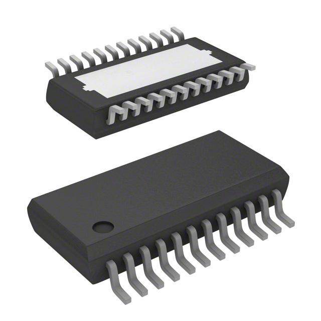
| 描述 | IC MOSFET DVR 3A DUAL HS 8-DIP门驱动器 3A Dual |
| 产品分类 | PMIC - MOSFET,电桥驱动器 - 外部开关集成电路 - IC |
| 品牌 | Microchip Technology |
| 产品手册 | |
| 产品图片 |
|
| rohs | 符合RoHS无铅 / 符合限制有害物质指令(RoHS)规范要求 |
| 产品系列 | 电源管理 IC,门驱动器,Microchip Technology TC4424EPA- |
| 数据手册 | http://www.microchip.com/mymicrochip/filehandler.aspx?ddocname=en011759 |
| 产品型号 | TC4424EPA |
| PCN组件/产地 | http://www.microchip.com/mymicrochip/NotificationDetails.aspx?id=5776&print=view |
| 上升时间 | 35 ns |
| 下降时间 | 35 ns |
| 产品 | MOSFET Gate Drivers |
| 产品种类 | 门驱动器 |
| 供应商器件封装 | 8-PDIP |
| 包装 | 管件 |
| 商标 | Microchip Technology |
| 安装类型 | 通孔 |
| 安装风格 | Through Hole |
| 封装 | Tube |
| 封装/外壳 | 8-DIP(0.300",7.62mm) |
| 封装/箱体 | PDIP-8 |
| 工作温度 | -40°C ~ 85°C |
| 工厂包装数量 | 60 |
| 延迟时间 | 33ns |
| 最大功率耗散 | 730 mW |
| 最大工作温度 | + 85 C |
| 最小工作温度 | - 40 C |
| 标准包装 | 60 |
| 激励器数量 | 2 Driver |
| 电压-电源 | 4.5 V ~ 18 V |
| 电流-峰值 | 3A |
| 电源电压-最大 | 18 V |
| 电源电压-最小 | 4.5 V |
| 电源电流 | 2.5 mA |
| 类型 | Low Side |
| 输入类型 | 非反相 |
| 输出数 | 2 |
| 输出端数量 | 2 |
| 配置 | Non-Inverting |
| 配置数 | 2 |
| 高压侧电压-最大值(自举) | - |


- 商务部:美国ITC正式对集成电路等产品启动337调查
- 曝三星4nm工艺存在良率问题 高通将骁龙8 Gen1或转产台积电
- 太阳诱电将投资9.5亿元在常州建新厂生产MLCC 预计2023年完工
- 英特尔发布欧洲新工厂建设计划 深化IDM 2.0 战略
- 台积电先进制程称霸业界 有大客户加持明年业绩稳了
- 达到5530亿美元!SIA预计今年全球半导体销售额将创下新高
- 英特尔拟将自动驾驶子公司Mobileye上市 估值或超500亿美元
- 三星加码芯片和SET,合并消费电子和移动部门,撤换高东真等 CEO
- 三星电子宣布重大人事变动 还合并消费电子和移动部门
- 海关总署:前11个月进口集成电路产品价值2.52万亿元 增长14.8%


PDF Datasheet 数据手册内容提取
TC4423/TC4424/TC4425 3A Dual High-Speed Power MOSFET Drivers Features General Description • High Peak Output Current: 3A The TC4423/TC4424/TC4425 devices are a family of (cid:127) Wide Input Supply Voltage Operating Range: 3A, dual-output buffers/MOSFET drivers. Pin compati- ble with the TC1426/27/28, TC4426/27/28 and - 4.5V to 18V TC4426A/27A/28A dual 1.5A driver families, the (cid:127) High Capacitive Load Drive Capability: TC4423/24/25 family has an increased latch-up current - 1800pF in 25ns rating of 1.5A, making them even more robust for (cid:127) Short Delay Times: <40ns (typ) operation in harsh electrical environments. (cid:127) Matched Rise/Fall Times As MOSFET drivers, the TC4423/TC4424/TC4425 can (cid:127) Low Supply Current: easily charge 1800pF gate capacitance in under - With Logic ‘1’ Input – 3.5mA (Max) 35nsec, providing low enough impedances in both the - With Logic ‘0’ Input – 350µA (Max) on and off states to ensure the MOSFET's intended state will not be affected, even by large transients. (cid:127) Low Output Impedance: 3.5 Ω (typ) (cid:127) Latch-Up Protected: Will Withstand 1.5A Reverse The TC4423/TC4424/TC4425 inputs may be driven Current directly from either TTL or CMOS (2.4V to 18V). In addition, the 300mV of built-in hysteresis provides (cid:127) Logic Input Will Withstand Negative Swing Up To noise immunity and allows the device to be driven from 5V slowly rising or falling waveforms. (cid:127) ESD Protected: 4kV (cid:127) Pin compatible with the TC1426/TC1427/TC1428, TC4426/TC4427/TC4428 and TC4426A/ TC4427A/TC4428A devices. (cid:127) Space-saving 8-Pin 6x5 DFN Package Applications (cid:127) Switch Mode Power Supplies (cid:127) Pulse Transformer Drive (cid:127) Line Drivers Package Types(1) 8-Pin PDIP TC4423 TC4424 TC4425 NC 1 8 NC NC NC 16-Pin SOIC (Wide) TC4423 TC4424 TC4425 IN A 2 TC4423 7 OUT A OUT A OUT A GND 3 TC4424 6 VDD VDD VDD NC 1 16 NC NC NC IN B 4 TC4425 5 OUT B OUT B OUT B IN A 2 15 OUT A OUT A OUT A NC 3 14 OUT A OUT A OUT A TC4423 8-Pin DFN(2) TC4423 TC4424 TC4425 GND 4 TC4424 13 VDD VDD VDD GND 5 TC4425 12 VDD VDD VDD NC 1 8 NC NC NC NC 6 11 OUT B OUT B OUT B TC4423 IN B 7 10 OUT B OUT B OUT B IN A 2 7 OUT A OUT A OUT A TC4424 NC 8 9 NC NC NC GND 3 TC4425 6 VDD VDD VDD IN B 4 5 OUT B OUT B OUT B Note1: Duplicate pins must both be connected for proper operation. 2: Exposed pad of the DFN package is electrically isolated. 2004 Microchip Technology Inc. DS21421D-page 1
TC4423/TC4424/TC4425 Functional Block Diagram(1) V DD Inverting 750µA 300mV Output Non-inverting Input Effective 4.7V Input C = 20pF TC4 423 Dual Inverting (Each Input) TC4 424 Dual Non-inverting TC4425 One Inverting, One Non-inverting GND Note 1: Unused inputs should be grounded. DS21421D-page 2 2004 Microchip Technology Inc.
TC4423/TC4424/TC4425 1.0 ELECTRICAL CHARACTERISTICS Absolute Maximum Ratings † Supply Voltage................................................................+22V Input Voltage, IN A or IN B ................................................(V + 0.3V) to (GND – 5V) DD Package Power Dissipation (T ≤ 70°C) A DFN......................................................................... Note2 PDIP.......................................................................730mW SOIC.......................................................................470mW † Notice: Stresses above those listed under "Maximum Ratings" may cause permanent damage to the device. This is a stress rating only and functional operation of the device at those or any other conditions above those indicated in the operational sections of this specification is not intended. Exposure to maximum rating conditions for extended periods may affect device reliability. DC CHARACTERISTICS Electrical Specifications: Unless otherwise indicated, T = +25°C, with 4.5V ≤ V ≤ 18V. A DD Parameters Sym Min Typ Max Units Conditions Input Logic ‘1’, High Input Voltage V 2.4 — — V IH Logic ‘0’, Low Input Voltage V — — 0.8 V IL Input Current I –1 — 1 µA 0V ≤ V ≤ V IN IN DD Output High Output Voltage V V – 0.025 — — V OH DD Low Output Voltage V — — 0.025 V OL Output Resistance, High R — 2.8 5 Ω I = 10mA, V = 18V OH OUT DD Output Resistance, Low R — 3.5 5 Ω I = 10mA, V = 18V OL OUT DD Peak Output Current I — 3 — A PK Latch-Up Protection With- I — >1.5 — A Duty cycle ≤ 2%, t ≤ 300µsec. REV stand Reverse Current Switching Time (Note1) Rise Time t — 23 35 ns Figure4-1, Figure4-2, R C = 1800pF L Fall Time t — 25 35 ns Figure4-1, Figure4-2, F C = 1800pF L Delay Time t — 33 75 ns Figure4-1, Figure4-2, D1 C = 1800pF L Delay Time t — 38 75 ns Figure4-1, Figure4-2, D2 C = 1800pF L Power Supply Power Supply Current I — 1.5 2.5 mA V = 3V (Both inputs) S IN — 0.15 0.25 V = 0V (Both inputs) IN Note 1: Switching times ensured by design. 2: Package power dissipation is dependent on the copper pad area on the PCB. 2004 Microchip Technology Inc. DS21421D-page 3
TC4423/TC4424/TC4425 DC CHARACTERISTICS (OVER OPERATING TEMPERATURE RANGE) Electrical Specifications: Unless otherwise indicated, operating temperature range with 4.5V ≤ V ≤ 18V. DD Parameters Sym Min Typ Max Units Conditions Input Logic ‘1’, High Input Voltage V 2.4 — — V IH Logic ‘0’, Low Input Voltage V — — 0.8 V IL Input Current I –10 — +10 µA 0V ≤ V ≤ V IN IN DD Output High Output Voltage V V – 0.025 — — V OH DD Low Output Voltage V — — 0.025 V OL Output Resistance, High R — 3.7 8 Ω I = 10mA, V = 18V OH OUT DD Output Resistance, Low R — 4.3 8 Ω I = 10mA, V = 18V OL OUT DD Peak Output Current I — 3.0 — A PK Latch-Up Protection I — >1.5 — A Duty cycle ≤ 2%, t ≤ 300µsec REV Withstand Reverse Current Switching Time (Note1) Rise Time t — 28 60 ns Figure4-1, Figure4-2, R C = 1800pF L Fall Time t — 32 60 ns Figure4-1, Figure4-2, F C = 1800pF L Delay Time t — 32 100 ns Figure4-1, Figure4-2, D1 C = 1800pF L Delay Time t — 38 100 ns Figure4-1, Figure4-2, D2 C = 1800pF L Power Supply Power Supply Current I — 2.0 3.5 mA V = 3V (Both inputs) S IN — 0.2 0.3 V = 0V (Both inputs) IN Note 1: Switching times ensured by design. TEMPERATURE CHARACTERISTICS Electrical Specifications: Unless otherwise noted, all parameters apply with 4.5V ≤ V ≤ 18V. DD Parameters Sym Min Typ Max Units Conditions Temperature Ranges Specified Temperature Range (C) T 0 — +70 °C A Specified Temperature Range (E) T –40 — +85 °C A Specified Temperature Range (V) T –40 — +125 °C A Maximum Junction Temperature T — — +150 °C J Storage Temperature Range T –65 — +150 °C A Package Thermal Resistances Thermal Resistance, 8L-6x5 DFN θ — 33.2 — °C/W Typical four-layer board with JA vias to ground plane Thermal Resistance, 8L-PDIP θ — 125 — °C/W JA Thermal Resistance, 16L-SOIC θ — 155 — °C/W JA DS21421D-page 4 2004 Microchip Technology Inc.
TC4423/TC4424/TC4425 2.0 TYPICAL PERFORMANCE CURVES Note: The graphs and tables provided following this note are a statistical summary based on a limited number of samples and are provided for informational purposes only. The performance characteristics listed herein are not tested or guaranteed. In some graphs or tables, the data presented may be outside the specified operating range (e.g., outside specified power supply range) and therefore outside the warranted range. 100 100 4700 pF 4700 pF 80 80 t (nsec)RISE 6400 32320000 ppFF (nsec)tFALL 6400 32320000 ppFF 20 1500 pF 20 1500 pF 1000 pF 1000 pF 470 pF 470 pF 0 0 4 6 8 10 12 14 16 18 4 6 8 10 12 14 16 18 VDD (V) VDD (V) FIGURE 2-1: Rise Time vs. Supply FIGURE 2-4: Fall Time vs. Supply Voltage. Voltage. 100 100 5V 5V 80 80 t (nsec)RISE 6400 1105VV (nsec)tFALL 6400 1105VV 20 20 0 0 100 1000 10,000 100 1000 10,000 CLOAD (pF) CLOAD (pF) FIGURE 2-2: Rise Time vs. Capacitive FIGURE 2-5: Fall Time vs. Capacitive Load. Load. 32 100 30 CLOAD = 2200 pF tFALL CVDLOD A=D 1 =0 V2200 pF 80 tD1 28 c) e s Time (nsec) 2264 tRISE tRISE Delay Time (n 6400 22 20 tFALL 20 tD2 18 -55 -35 -15 5 25 45 65 85 105 125 0 1 2 3 4 5 6 7 8 9 10 11 12 TA (°C) Input (V) FIGURE 2-3: Rise and Fall Times vs. FIGURE 2-6: Propagation Delay vs. Input Temperature. Amplitude. 2004 Microchip Technology Inc. DS21421D-page 5
TC4423/TC4424/TC4425 Typical Performance Curves (Continued) 50 50 CLOAD = 2200 pF CLOAD = 2200 pF 45 45 tD2 Delay Time (nsec) 433050 ttDD12 Delay Time (nsec) 433050 tD1 25 25 20 20 4 6 8 10 12 14 16 18 -55 -35 -15 5 25 45 65 85 105 125 VDD (V) TA (°C) FIGURE 2-7: Propagation Delay Time vs. FIGURE 2-10: Propagation Delay Time vs. Supply Voltage. Temperature. 1.4 TA = 25°C Both Inputs = 1 1.2 1 mA) mA) 1.0 I (QUIESCENT0.1 Both Inputs = 0 I (QUIESCENT 000...864 Both Inputs = 1 0.2 Both Inputs = 0 0.01 0.0 4 6 8 10 12 14 16 18 -55 -35 -15 5 25 45 65 85 105 125 VDD (V) TA (°C) FIGURE 2-8: Quiescent Current vs. FIGURE 2-11: Quiescent Current vs. Supply Voltage. Temperature. 14 14 12 12 Worst Case Worst Case 10 @ TJ = +150°C 10 @ TJ = +150°C Ω) Ω) (ON) 8 (ON) 8 S( S( D D R R 6 6 Typical @ Typical @ 4 TA = +25°C 4 TA = +25°C 2 2 4 6 8 10 12 14 16 18 4 6 8 10 12 14 16 18 VDD (V) VDD (V) FIGURE 2-9: Output Resistance FIGURE 2-12: Output Resistance (Output High) vs. Supply Voltage. (Output Low) vs. Supply Voltage. DS21421D-page 6 2004 Microchip Technology Inc.
TC4423/TC4424/TC4425 Typical Performance Curves (Continued) Note: Load on single output only 60 60 VDD = 18V VDD = 18V 3300 pF 50 50 1000 pF 634 kHz 40 40 A) A) m m (UPPLY30 355 kHz (UPPLY 30 10,000 pF IS20 IS 20 100 pF 200 kHz 63.4 kHz 10 112.5 kHz 35.5 kHz 10 20 kHz 0 0 100 1000 10,000 10 100 1000 CLOAD (pF) Frequency (kHz) FIGURE 2-13: Supply Current vs. FIGURE 2-16: Supply Current vs. Capacitive Load. Frequency. 90 90 80 VDD = 12V 80 VDD = 12V 3300 pF 2 MHz 1000 pF 70 70 60 60 A) A) m 50 m 50 I (SUPPLY4300 16.3142 5k HMzHz 200 kHz I (SUPPLY 4300 10,000 pF 100 pF 20 355 kHz 112.5 kHz 20 10 63.4 kHz 10 20 kHz 0 0 100 1000 10,000 10 100 1000 CLOAD (pF) Frequency (kHz) FIGURE 2-14: Supply Current vs. FIGURE 2-17: Supply Current vs. Capacitive Load. Frequency. 120 120 4700 pF VDD = 6V VDD = 6V 100 100 10,000 pF 80 80 mA) 1.125 MHz mA) 2200 pF I (SUPPLY 6400 3.55 MHz 634 kHz I (SUPPLY 6400 1100000 p pFF 2 MHz 355 kHz 20 20 112.5 kHz 0 20 kHz 0 100 1000 10,000 10 100 1000 CLOAD (pF) Frequency (kHz) FIGURE 2-15: Supply Current vs. FIGURE 2-18: Supply Current vs. Capacitive Load. Frequency. 2004 Microchip Technology Inc. DS21421D-page 7
TC4423/TC4424/TC4425 Typical Performance Curves (Continued) 10-7 8 6 4 2 c se 10-8 A (cid:127) 8 6 4 2 10-9 0 2 4 6 8 10 12 14 16 18 VIN (V) Note: The values on this graph represent the loss seen by both drivers in a package during one complete cycle. For a single driver, divide the stated values by 2. For a single transition of a single driver, divide the stated value by 4. FIGURE 2-19: TC4423 Crossover Energy. DS21421D-page 8 2004 Microchip Technology Inc.
TC4423/TC4424/TC4425 3.0 PIN DESCRIPTIONS The descriptions of the pins are listed in Table3-1. TABLE 3-1: PIN FUNCTION TABLE (1) 16-Pin 8-Pin 8-Pin PDIP SOIC Symbol Description DFN (Wide) 1 1 1 NC No connection 2 2 2 IN A Input A — — 3 NC No connection 3 3 4 GND Ground — — 5 GND Ground — — 6 NC No connection 4 4 7 IN B Input B — — 8 NC No connection — — 9 NC No connection 5 5 10 OUT B Output B — — 11 OUT B Output B 6 6 12 V Supply input DD — — 13 V Supply input DD 7 7 14 OUT A Output A — — 15 OUT A Output A 8 8 16 NC No connection — PAD — NC Exposed Metal Pad Note 1: Duplicate pins must be connected for proper operation. 3.1 Inputs A and B 3.4 Ground (GND) Inputs A and B are TTL/CMOS compatible inputs that Ground is the device return pin. The ground pin(s) control outputs A and B, respectively. These inputs should have a low-impedance connection to the bias have 300mV of hysteresis between the high and low supply source return. High peak currents will flow out input levels, allowing them to be driven from slow rising the ground pin(s) when the capacitive load is being and falling signals, and to provide noise immunity. discharged. 3.2 Outputs A and B 3.5 Exposed Metal Pad Outputs A and B are CMOS push-pull outputs that are The exposed metal pad of the 6x5 DFN package is not capable of sourcing and sinking 3A peaks of current internally connected to any potential. Therefore, this (V = 18V). The low output impedance ensures the pad can be connected to a ground plane or other cop- DD gate of the external MOSFET will stay in the intended per plane on a printed circuit board to aid in heat state even during large transients. These outputs also removal from the package. have a reverse current latch-up rating of 1.5A. 3.3 Supply Input (V ) DD V is the bias supply input for the MOSFET driver and DD has a voltage range of 4.5V to 18V. This input must be decoupled to ground with a local ceramic capacitor. This bypass capacitor provides a localized low- impedance path for the peak currents that are to be provided to the load. 2004 Microchip Technology Inc. DS21421D-page 9
TC4423/TC4424/TC4425 4.0 APPLICATIONS INFORMATION V = 18V V = 18V DD DD 1µF 0.1µF 1µF 0.1µF WIMA Ceramic WIMA Ceramic MKS-2 MKS-2 Input 1 Output Input 1 Output CL = 1800pF CL = 1800pF 2 2 TC4423 TC4424 (1/2 TC4425) (1/2 TC4425) Input: 100kHz, Input: 100kHz, square wave, square wave, tRISE = tFALL ≤ 10ns tRISE = tFALL ≤ 10ns +5V 90% +5V 90% Input Input 10% 0V 10% tD1 tD2 0V t t 18V 90% F R 90% 18V tD190% tD2 90% Output Output tR tF 0V 10% 10% 0V 10% 10% FIGURE 4-1: Inverting Driver Switching FIGURE 4-2: Non-inverting Driver Time. Switching Time. DS21421D-page 10 2004 Microchip Technology Inc.
TC4423/TC4424/TC4425 5.0 PACKAGING INFORMATION 5.1 Package Marking Information 8-Lead DFN Example: XXXXXXX TC4423 XXXXXXX EMF XXYYWW 0420 NNN 256 8-Lead PDIP (300 mil) Example: XXXXXXXX TC4423 XXXXXNNN CPA256 YYWW 0420 16-Lead SOIC (300 mil) Example: XXXXXXXXXXX TC4423COE XXXXXXXXXXX XXXXXXXXXXX YYWWNNN 0420256 Legend: XX...X Customer specific information* YY Year code (last 2 digits of calendar year) WW Week code (week of January 1 is week ‘01’) NNN Alphanumeric traceability code Note: In the event the full Microchip part number cannot be marked on one line, it will be carried over to the next line thus limiting the number of available characters for customer specific information. * Standard marking consists of Microchip part number, year code, week code, traceability code (facility code, mask rev#, and assembly code). For marking beyond this, certain price adders apply. Please check with your Microchip Sales Office. 2004 Microchip Technology Inc. DS21421D-page 11
TC4423/TC4424/TC4425 8-Lead Plastic Dual Flat No Lead Package (MF) 6x5 mm Body (DFN-S) – Saw Singulated DS21421D-page 12 2004 Microchip Technology Inc.
TC4423/TC4424/TC4425 8-Lead Plastic Dual In-line (P) – 300 mil (PDIP) E1 D 2 n 1 α E A A2 L c A1 β B1 p eB B Units INCHES* MILLIMETERS Dimension Limits MIN NOM MAX MIN NOM MAX Number of Pins n 8 8 Pitch p .100 2.54 Top to Seating Plane A .140 .155 .170 3.56 3.94 4.32 Molded Package Thickness A2 .115 .130 .145 2.92 3.30 3.68 Base to Seating Plane A1 .015 0.38 Shoulder to Shoulder Width E .300 .313 .325 7.62 7.94 8.26 Molded Package Width E1 .240 .250 .260 6.10 6.35 6.60 Overall Length D .360 .373 .385 9.14 9.46 9.78 Tip to Seating Plane L .125 .130 .135 3.18 3.30 3.43 Lead Thickness c .008 .012 .015 0.20 0.29 0.38 Upper Lead Width B1 .045 .058 .070 1.14 1.46 1.78 Lower Lead Width B .014 .018 .022 0.36 0.46 0.56 Overall Row Spacing § eB .310 .370 .430 7.87 9.40 10.92 Mold Draft Angle Top α 5 10 15 5 10 15 Mold Draft Angle Bottom β 5 10 15 5 10 15 * Controlling Parameter § Significant Characteristic Notes: Dimensions D and E1 do not include mold flash or protrusions. Mold flash or protrusions shall not exceed .010” (0.254mm) per side. JEDEC Equivalent: MS-001 Drawing No. C04-018 2004 Microchip Technology Inc. DS21421D-page 13
TC4423/TC4424/TC4425 16-Lead Plastic Small Outline (SO) – Wide, 300 mil (SOIC) E p E1 D 2 n 1 B h α 45° c A A2 φ β L A1 Units INCHES* MILLIMETERS Dimension Limits MIN NOM MAX MIN NOM MAX Number of Pins n 16 16 Pitch p .050 1.27 Overall Height A .093 .099 .104 2.36 2.50 2.64 Molded Package Thickness A2 .088 .091 .094 2.24 2.31 2.39 Standoff § A1 .004 .008 .012 0.10 0.20 0.30 Overall Width E .394 .407 .420 10.01 10.34 10.67 Molded Package Width E1 .291 .295 .299 7.39 7.49 7.59 Overall Length D .398 .406 .413 10.10 10.30 10.49 Chamfer Distance h .010 .020 .029 0.25 0.50 0.74 Foot Length L .016 .033 .050 0.41 0.84 1.27 Foot Angle φ 0 4 8 0 4 8 Lead Thickness c .009 .011 .013 0.23 0.28 0.33 Lead Width B .014 .017 .020 0.36 0.42 0.51 Mold Draft Angle Top α 0 12 15 0 12 15 Mold Draft Angle Bottom β 0 12 15 0 12 15 * Controlling Parameter § Significant Characteristic Notes: Dimensions D and E1 do not include mold flash or protrusions. Mold flash or protrusions shall not exceed .010” (0.254mm) per side. JEDEC Equivalent: MS-013 Drawing No. C04-102 DS21421D-page 14 2004 Microchip Technology Inc.
TC4423/TC4424/TC4425 PRODUCT IDENTIFICATION SYSTEM To order or obtain information, e.g., on pricing or delivery, refer to the factory or the listed sales office. PART NO. X XX XXX X Examples: a) TC4423COE: 3A Dual Inverting Device Temperature Package Tape & Reel PB Free MOSFET Driver, Range 0°C to +70°C, 16LD SOIC package. Device: TC4423: 3A Dual MOSFET Driver, Inverting b) TC4423CPA: 3A Dual Inverting TC4424: 3A Dual MOSFET Driver, Non-Inverting MOSFET Driver, TC4425: 3A Dual MOSFET Driver, Complementary 0°C to +70°C, 8LD PDIP package. Temperature Range: C = 0°C to +70°C (PDIP & SOIC Only) c) TC4423VMF: 3A Dual Inverting E = -40°C to +85°C MOSFET Driver, V = -40°C to +125°C -40°C to +125°C, 8LD DFN package. Package: MF = Dual, Flat, No-Lead (6x5 mm Body), 8-lead a) TC4424COE713: 3A Dual Non-Inverting, MF713 = Dual, Flat, No-Lead (6x5 mm Body), 8-lead MOSFET Driver, (Tape and Reel) OE = SOIC (Wide), 16-pin 0°C to +70°C, OE713 = SOIC (Wide), 16-pin (Tape and Reel) 16LD SOIC package, PA = Plastic DIP, (300 mil body), 8-lead Tape and Reel. b) TC4424EPA: 3A Dual Non-Inverting, PB Free: G = Lead-Free device * MOSFET Driver, = Blank -40°C to +85°C, 8LD PDIP package. * Available on selected packages. Contact your local sales representative for availability. a) TC4425EOE: 3A Dual Complementary, MOSFET Driver, -40°C to +85°C, 16LD SOIC package. b) TC4425CPA: 3A Dual Complementary, MOSFET Driver, 0°C to +70°C, PDIP package. Sales and Support Data Sheets Products supported by a preliminary Data Sheet may have an errata sheet describing minor operational differences and recommended workarounds. To determine if an errata sheet exists for a particular device, please contact one of the following: 1. Your local Microchip sales office 2. The Microchip Corporate Literature Center U.S. FAX: (480) 792-7277 3. The Microchip Worldwide Site (www.microchip.com) Please specify which device, revision of silicon and Data Sheet (include Literature #) you are using. Customer Notification System Register on our web site (www.microchip.com/cn) to receive the most current information on our products. 2004 Microchip Technology Inc. DS21421D-page 15
TC4423/TC4424/TC4425 NOTES: DS21421D-page 16 2004 Microchip Technology Inc.
Note the following details of the code protection feature on Microchip devices: (cid:127) Microchip products meet the specification contained in their particular Microchip Data Sheet. (cid:127) Microchip believes that its family of products is one of the most secure families of its kind on the market today, when used in the intended manner and under normal conditions. (cid:127) There are dishonest and possibly illegal methods used to breach the code protection feature. All of these methods, to our knowledge, require using the Microchip products in a manner outside the operating specifications contained in Microchip’s Data Sheets. Most likely, the person doing so is engaged in theft of intellectual property. (cid:127) Microchip is willing to work with the customer who is concerned about the integrity of their code. (cid:127) Neither Microchip nor any other semiconductor manufacturer can guarantee the security of their code. Code protection does not mean that we are guaranteeing the product as “unbreakable.” Code protection is constantly evolving. We at Microchip are committed to continuously improving the code protection features of our products. Attempts to break Microchip’s code protection feature may be a violation of the Digital Millennium Copyright Act. If such acts allow unauthorized access to your software or other copyrighted work, you may have a right to sue for relief under that Act. Information contained in this publication regarding device Trademarks applications and the like is intended through suggestion only The Microchip name and logo, the Microchip logo, Accuron, and may be superseded by updates. It is your responsibility to dsPIC, KEELOQ, microID, MPLAB, PIC, PICmicro, ensure that your application meets with your specifications. PICSTART, PROMATE, PowerSmart, rfPIC, and No representation or warranty is given and no liability is SmartShunt are registered trademarks of Microchip assumed by Microchip Technology Incorporated with respect Technology Incorporated in the U.S.A. and other countries. to the accuracy or use of such information, or infringement of patents or other intellectual property rights arising from such AmpLab, FilterLab, MXDEV, MXLAB, PICMASTER, SEEVAL, use or otherwise. Use of Microchip’s products as critical SmartSensor and The Embedded Control Solutions Company components in life support systems is not authorized except are registered trademarks of Microchip Technology with express written approval by Microchip. No licenses are Incorporated in the U.S.A. conveyed, implicitly or otherwise, under any intellectual Analog-for-the-Digital Age, Application Maestro, dsPICDEM, property rights. dsPICDEM.net, dsPICworks, ECAN, ECONOMONITOR, FanSense, FlexROM, fuzzyLAB, In-Circuit Serial Programming, ICSP, ICEPIC, Migratable Memory, MPASM, MPLIB, MPLINK, MPSIM, PICkit, PICDEM, PICDEM.net, PICLAB, PICtail, PowerCal, PowerInfo, PowerMate, PowerTool, rfLAB, rfPICDEM, Select Mode, Smart Serial, SmartTel and Total Endurance are trademarks of Microchip Technology Incorporated in the U.S.A. and other countries. SQTP is a service mark of Microchip Technology Incorporated in the U.S.A. All other trademarks mentioned herein are property of their respective companies. © 2004, Microchip Technology Incorporated, Printed in the U.S.A., All Rights Reserved. Printed on recycled paper. Microchip received ISO/TS-16949:2002 quality system certification for its worldwide headquarters, design and wafer fabrication facilities in Chandler and Tempe, Arizona and Mountain View, California in October 2003. The Company’s quality system processes and procedures are for its PICmicro® 8-bit MCUs, KEELOQ® code hopping devices, Serial EEPROMs, microperipherals, nonvolatile memory and analog products. In addition, Microchip’s quality system for the design and manufacture of development systems is ISO 9001:2000 certified. 2004 Microchip Technology Inc. DS21421D-page 17
WORLDWIDE SALES AND SERVICE AMERICAS ASIA/PACIFIC ASIA/PACIFIC EUROPE Corporate Office Australia - Sydney India - Bangalore Austria - Weis 2355 West Chandler Blvd. Tel: 61-2-9868-6733 Tel: 91-80-2229-0061 Tel: 43-7242-2244-399 Chandler, AZ 85224-6199 Fax: 61-2-9868-6755 Fax: 91-80-2229-0062 Fax: 43-7242-2244-393 Tel: 480-792-7200 China - Beijing India - New Delhi Denmark - Ballerup Fax: 480-792-7277 Tel: 86-10-8528-2100 Tel: 91-11-5160-8632 Tel: 45-4420-9895 Technical Support: Fax: 86-10-8528-2104 Fax: 91-11-5160-8632 Fax: 45-4420-9910 480-792-7627 Web Address: China - Chengdu Japan - Kanagawa France - Massy www.microchip.com Tel: 86-28-8676-6200 Tel: 81-45-471- 6166 Tel: 33-1-69-53-63-20 Fax: 86-28-8676-6599 Fax: 81-45-471-6122 Fax: 33-1-69-30-90-79 Atlanta Alpharetta, GA China - Fuzhou Korea - Seoul Germany - Ismaning Tel: 770-640-0034 Tel: 86-591-750-3506 Tel: 82-2-554-7200 Tel: 49-89-627-144-0 Fax: 770-640-0307 Fax: 86-591-750-3521 Fax: 82-2-558-5932 or Fax: 49-89-627-144-44 China - Hong Kong SAR 82-2-558-5934 Italy - Milan Boston Westford, MA Tel: 852-2401-1200 Singapore Tel: 39-0331-742611 Tel: 978-692-3848 Fax: 852-2401-3431 Tel: 65-6334-8870 Fax: 39-0331-466781 Fax: 978-692-3821 China - Shanghai Fax: 65-6334-8850 Netherlands - Drunen Chicago Tel: 86-21-6275-5700 Taiwan - Kaohsiung Tel: 31-416-690399 Itasca, IL Fax: 86-21-6275-5060 Tel: 886-7-536-4816 Fax: 31-416-690340 Tel: 630-285-0071 China - Shenzhen Fax: 886-7-536-4817 England - Berkshire Fax: 630-285-0075 Tel: 86-755-8290-1380 Taiwan - Taipei Tel: 44-118-921-5869 Dallas Fax: 86-755-8295-1393 Tel: 886-2-2500-6610 Fax: 44-118-921-5820 Addison, TX China - Shunde Fax: 886-2-2508-0102 Tel: 972-818-7423 Tel: 86-757-2839-5507 Taiwan - Hsinchu Fax: 972-818-2924 Fax: 86-757-2839-5571 Tel: 886-3-572-9526 Detroit China - Qingdao Fax: 886-3-572-6459 Farmington Hills, MI Tel: 86-532-502-7355 Tel: 248-538-2250 Fax: 86-532-502-7205 Fax: 248-538-2260 Kokomo Kokomo, IN Tel: 765-864-8360 Fax: 765-864-8387 Los Angeles Mission Viejo, CA Tel: 949-462-9523 Fax: 949-462-9608 San Jose Mountain View, CA Tel: 650-215-1444 Fax: 650-961-0286 Toronto Mississauga, Ontario, Canada Tel: 905-673-0699 Fax: 905-673-6509 08/24/04 DS21421D-page 18 2004 Microchip Technology Inc.
Mouser Electronics Authorized Distributor Click to View Pricing, Inventory, Delivery & Lifecycle Information: M icrochip: TC4424VMF713 TC4423VMF713 TC4425VMF713 TC4423MJA TC4423VOE TC4423VOE713 TC4425VOE713 TC4424VOE713 TC4423CPA TC4423COE TC4424EMF TC4424EOE TC4424EPA TC4425EPA TC4425EOE TC4425EMF TC4425CPA TC4424MJA TC4423EPA TC4425COE TC4423EMF TC4424COE713 TC4425COE713 TC4423COE713 TC4423EOE TC4424COE TC4424CPA TC4423EMF713 TC4425EMF713 TC4424EMF713 TC4423EOE713 TC4424EOE713 TC4425EOE713 TC4423VPA TC4423VMF TC4425VPA TC4424VPA TC4424VOE TC4424VMF TC4425VOE TC4425VMF