 Datasheet下载
- 型号: DVIULC6-4SC6
- 制造商: STMicroelectronics
- 库位|库存: xxxx|xxxx
- 要求:
| 数量阶梯 | 香港交货 | 国内含税 |
| +xxxx | $xxxx | ¥xxxx |
查看当月历史价格
查看今年历史价格
DVIULC6-4SC6产品简介:
ICGOO电子元器件商城为您提供DVIULC6-4SC6由STMicroelectronics设计生产,在icgoo商城现货销售,并且可以通过原厂、代理商等渠道进行代购。 DVIULC6-4SC6价格参考¥1.45-¥1.80。STMicroelectronicsDVIULC6-4SC6封装/规格:TVS - 二极管, 。您可以下载DVIULC6-4SC6参考资料、Datasheet数据手册功能说明书,资料中有DVIULC6-4SC6 详细功能的应用电路图电压和使用方法及教程。
STMicroelectronics的DVIULC6-4SC6是一款瞬态电压抑制(TVS)二极管,主要用于保护电子设备免受瞬态电压波动和静电放电(ESD)的损害。这款二极管广泛应用于消费电子、通信设备、工业控制和其他对电压敏感的电路中。

 应用场景:

1. 消费电子产品:
   - 显示器和电视:用于保护HDMI、DisplayPort等接口,防止因外部设备连接时产生的瞬态电压或静电放电对内部电路造成损坏。
   - 智能手机和平板电脑:保护USB接口、耳机插孔等外部连接端口,确保设备在插入或拔出外设时不会因电压波动而受损。
   - 音频设备:如音响系统中的线路输入输出接口,防止信号线引入的瞬态电压对敏感的音频芯片造成损害。

2. 通信设备:
   - 路由器和交换机:保护以太网端口、Wi-Fi模块等通信接口,防止雷击或电力波动引起的过电压。
   - 调制解调器:保护电话线或光纤接口,避免因外部干扰或电压突变导致设备故障。

3. 工业控制:
   - PLC(可编程逻辑控制器):保护输入输出端口,确保在恶劣环境下(如工厂车间)设备能够稳定运行,不受瞬态电压的影响。
   - 传感器和执行器:保护与主控系统的通信接口,确保数据传输的可靠性和安全性。

4. 汽车电子:
   - 车载信息娱乐系统:保护USB充电接口、蓝牙模块等,防止因车辆启动或电池电压波动对系统造成损害。
   - 摄像头和雷达系统:保护传感器接口,确保在复杂电磁环境下系统的正常工作。

5. 医疗设备:
   - 便携式医疗仪器:如血糖仪、心率监测仪等,保护电源接口和数据传输接口,确保设备的安全性和可靠性。
   - 大型医疗设备:如X光机、超声波设备等,保护其对外部设备的连接接口,防止外界干扰影响诊断结果。

总之,DVIULC6-4SC6 TVS二极管通过提供快速响应和高效保护,确保各类电子设备在面对瞬态电压威胁时能够保持稳定运行,延长设备使用寿命并提高系统可靠性。
| 参数 | 数值 |
| 产品目录 | |
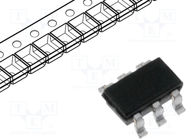
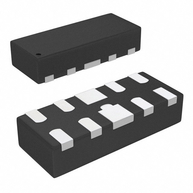
| 描述 | TVS DIODE 5VWM 17VC SOT23-6TVS二极管阵列 ESD PROTECTION |
| 产品分类 | |
| 品牌 | STMicroelectronics |
| 产品手册 | |
| 产品图片 |
|
| rohs | 符合RoHS无铅 / 符合限制有害物质指令(RoHS)规范要求 |
| 产品系列 | 二极管与整流器,TVS二极管,TVS二极管阵列,STMicroelectronics DVIULC6-4SC6DVI |
| 数据手册 | |
| 产品型号 | DVIULC6-4SC6 |
| 不同频率时的电容 | 0.85pF @ 1MHz |
| 产品目录页面 | |
| 产品种类 | TVS二极管阵列 |
| 供应商器件封装 | SOT-23-6 |
| 其它名称 | 497-5237-2 |
| 其它有关文件 | http://www.st.com/web/catalog/sense_power/FM114/CL1137/SC1490/PF109008?referrer=70071840http://www.st.com/web/catalog/sense_power/FM114/CL1137/SC1767/PF109008?referrer=70071840 |
| 击穿电压 | 6 V |
| 功率-峰值脉冲 | 80W |
| 包装 | 带卷 (TR) |
| 单向通道 | - |
| 双向通道 | 4 |
| 商标 | STMicroelectronics |
| 外壳高度 | 1.3 mm |
| 安装类型 | 表面贴装 |
| 安装风格 | SMD/SMT |
| 封装 | Reel |
| 封装/外壳 | SOT-23-6 |
| 封装/箱体 | SOT-23-6L |
| 尺寸 | 1.75 mm W x 3.05 mm L x 1.3 mm H |
| 峰值脉冲功率耗散 | 80 W |
| 工作温度 | -40°C ~ 125°C (TJ) |
| 工具箱 | /product-detail/zh/Q7525712/497-8023-KIT-ND/4158066/product-detail/zh/Q7525688/497-8022-KIT-ND/4158065/product-detail/zh/Q3108517/497-8009-KIT-ND/1306141 |
| 工厂包装数量 | 3000 |
| 应用 | 通用 |
| 最大工作温度 | + 125 C |
| 最小工作温度 | - 40 C |
| 极性 | Bidirectional |
| 标准包装 | 3,000 |
| 电压-击穿(最小值) | 6V |
| 电压-反向关态(典型值) | 5V |
| 电压-箝位(最大值)@Ipp | 17V |
| 电容 | 1 pF |
| 电流-峰值脉冲(10/1000µs) | 5A (8/20µs) |
| 电源线路保护 | 是 |
| 端接类型 | SMD/SMT |
| 类型 | 转向装置(轨至轨) |
| 系列 | DVIULC6 |
| 通道 | 4 Channels |
| 钳位电压 | 12 V |


- 商务部:美国ITC正式对集成电路等产品启动337调查
- 曝三星4nm工艺存在良率问题 高通将骁龙8 Gen1或转产台积电
- 太阳诱电将投资9.5亿元在常州建新厂生产MLCC 预计2023年完工
- 英特尔发布欧洲新工厂建设计划 深化IDM 2.0 战略
- 台积电先进制程称霸业界 有大客户加持明年业绩稳了
- 达到5530亿美元!SIA预计今年全球半导体销售额将创下新高
- 英特尔拟将自动驾驶子公司Mobileye上市 估值或超500亿美元
- 三星加码芯片和SET,合并消费电子和移动部门,撤换高东真等 CEO
- 三星电子宣布重大人事变动 还合并消费电子和移动部门
- 海关总署:前11个月进口集成电路产品价值2.52万亿元 增长14.8%


PDF Datasheet 数据手册内容提取
DVIULC6-4SC6 Ultralow capacitance ESD protection Datasheet production data Features ■ 4-line ESD protection (IEC 61000-4-2) ■ Protects V when applicable BUS ■ Ultralow capacitance: 0.6 pF at 825 MHz ■ Fast response time compared with varistors SOT23-6L ■ SOT23-6L package (JEDEC MO178AB) ■ RoHS compliant Benefits Applications ■ ESD standards compliance guaranteed at ■ DVI ports up to 1.65 Gb/s device level, hence greater immunity at system ■ HDMI ports up to 1.65 Gb/s level ■ IEEE 1394a, and b up to 1.6Gb/s ■ ESD protection of V , when applicable, BUS allows ESD current flowing to ground when ■ USB 2.0 ports up to 480 Mb/s (high speed), ESD event occurs on data line backwards compatible with USB 1.1 low and full speed ■ Optimized rise and fall times for maximum data integrity ■ Ethernet port: 10/100/1000 Mb/s ■ Consistent D+ / D- signal balance: ■ SIM card protection – Optimum capacitance matching tolerance ■ Video line protection for ultralow intra-pair skew: I/O to ground = 0.015 pF, Description I/O to I/O = 0.007 pF – Matching high bit rate DVI, HDMI, and The DVIULC6-4SC6 is a monolithic, application IEEE1394 requirements specific discrete device dedicated to ESD ■ Low PCB space occupation: 9mm2 protection of high speed interfaces, such as DVI, HDMI, IEEE1394a, and b, USB 2.0, Ethernet ■ Low leakage current for longer operation of links and video lines. battery powered devices Its ultralow line capacitance secures a high level ■ Higher reliability offered by monolithic of signal integrity without compromise in integration protecting sensitive chips against the most stringently characterized ESD strikes. Complies with these standards ■ IEC 61000-4-2 level 4: – ±15 kV (air discharge) – ±8 kV (contact discharge) ■ MIL STD883G-Method 3015-7 September 2012 Doc ID 11599 Rev 4 1/12 This is information on a product in full production. www.st.com 12
Characteristics DVIULC6-4SC6 1 Characteristics Figure 1. Functional diagram I/O1 11 6 I/O4 GND 2 5 VBUS I/O2 3 4 I/O3 T able 1. Absolute ratings Symbol Parameter Value Unit IEC 61000-4-2 air discharge ±15 V Peak pulse voltage IEC 61000-4-2 contact discharge ±15 kV PP MIL STD883G-Method 3015-7 ±25 P Peak pulse power 80 W pp T Storage temperature range -55 to +150 °C stg T Operating junction temperature range -40 to +125 °C j T Lead solder temperature (10 seconds duration) 260 °C L T able 2. Electrical characteristics (T = 25 °C) amb Value Symbol Parameter Test conditions Unit Min. Typ. Max. I Leakage current V = 5 V - - 0.5 µA RM RM Breakdown voltage V I = 1 mA 6 - - V BR between V and GND R BUS I = 1 A, t = 8/20 µs PP p - - 12 V Any I/O pin to GND V Clamping voltage CL I = 5 A, t = 8/20 µs PP p - - 17 V Any I/O pin to GND Capacitance between I/O VR = 0 V, F= 1 MHz - 0.85 1 C i/o-GND and GND V = 0 V, F= 825 MHz - 0.6 - R pF C Capacitance variation i/o- - - 0.015 - between I/O and GND GND V = 0 V, F= 1 MHz - 0.42 0.5 R C Capacitance between I/O i/o-i/o V = 0 V, F= 825 MHz - 0.3 - R pF Capacitance variation C - - 0.007 - i/o-i/o between I/O 2/12 Doc ID 11599 Rev 4
DVIULC6-4SC6 Characteristics Figure 2. L ine capacitance versus line Figure 3. Line capacitance versus frequency voltage (typical values) (typical values) C(pF) C(pF) 1.0 1.0 00..98 VosVTFcBj==U=58S02205O5m°MPCVEHRNzMS 00..89 VVVoI-sTBOcUj=/G=S3N2O0D5mP=°VEC 0RNVMS 0.7 0.7 0.6 0.6 0.5 CI/O- GND 0.5 CI/O- GND 0.4 0.4 0.3 0.3 0.2 0.2 0.1 Data line voltage (v) 0.1 F(MHz) CI/O-CI/O 0 0 0.0 0.5 1.0 1.5 2.0 2.5 3.0 3.5 4.0 1 10 100 1000 10000 Figure 4. R elative variation of leakage Figure 5. Frequency response current versus junction temperature (typical values) IRM[Tj] /IRM[Tj=25°C] S21(dB) Attenuation 5 0 4 -2 3 -4 2 -6 Tj(°C) F(Hz) 1 -8 25 50 75 100 125 111000000...000kkk 111...000MMM 111000...000MMM 111000000...000MMM 111...000GGG Figure 6. Remaining voltage after the Figure 7. Remaining voltage after the DVIULC6-4SC6 during DVIULC6-4SC6 during positive ESD surge(1) negative ESD surge(1) 1. measurements were done with DVIULC-4SC6 in open circuit Doc ID 11599 Rev 4 3/12
Characteristics DVIULC6-4SC6 Figure 8. Analog crosstalk results dB 0.00 -30.00 -60.00 -90.00 F (Hz) -120.00 100.0k 1.0M 10.0M 100.0M 1.0G 4/12 Doc ID 11599 Rev 4
DVIULC6-4SC6 Application examples 2 Application examples Figure 9. DVI/HDMI digital single link application HOST (PC,graphics cards,set-top box,DVD player) Display (LCD monitor,flat panel,display,projector) Tx0- RX0- Tx0+ RX0+ DVI connector TMDS TMDS DE Transmitter 11 6 11 6 Receiver DE Pixel 2 5 2 5 Pixel Data 3 4 3 4 Data GCoranptrhoicllser VCsloycnkc TTTTxxxx1122-+-+ RRRRxxxX1122-+-+ VCsloycnkc DCiosnptlraoyller Hsync 11 6 11 6 Hsync 2 5 TMDS Links 2 5 3 4 3 4 TC- RC- TC+ RC+ Figure 10. T1/E1/Ethernet protection Tx SMP75-8 +VCC DATA 4 3 5 2 100nF 6 11 TRANSCEIVER Rx SMP75-8 Doc ID 11599 Rev 4 5/12
Technical information DVIULC6-4SC6 3 Technical information 3.1 Surge protection The DVIULC6-4SC6 is particularly optimized to perform ESD surge protection based on the rail to rail topology. The clamping voltage V can be calculated as follows: CL V + = V + V for positive surges CL BUS F, V - = - V for negative surges CL F, with: V = V + R .I F T d p V = forward drop voltage, V = forward drop threshold voltage) F T Calculation example We can assume that the value of the dynamic resistance of the clamping diode is typically: R = 1.4 and V = 1.2 V. d T For an IEC 61000-4-2 surge Level 4 (Contact Discharge: V = 8 kV, R = 330 ), g g V = +5 V, and, in a first approximation, we assume that: I = V / R = 24 A. BUS p g g We find: V + = +39 V CL V - = -34 V CL Note: The calculations do not take into account phenomena due to parasitic inductances. 3.2 Surge protection application example If we consider that the connections from the pin V to V and from GND to PCB GND BUS CC plane are two tracks 10 mm long and 0.5 mm wide, we can assume that the parasitic inductances, L of these tracks are about 6 nH. So when an IEC 61000-4-2 surge occurs, W due to the rise time of this spike (tr = 1 ns), the voltage V has an extra value equal to CL L ·dI/dt. W The dI/dt is calculated as: dI/dt = I /t = 24 A/ns for an IEC 61000-4-2 surge level 4 (contact p r discharge V = 8 kV, R = 330 g g The over voltage due to the parasitic inductances is: L .dI/dt = 6 x 24 = 144 V W By taking into account the effect of these parasitic inductances due to unsuitable layout, the clamping voltage will be: V + = +39 + 144 = 183 V CL V - = -34 - 144 = -178 V CL We can reduce as much as possible these phenomena with simple layout optimization. This is the reason why some recommendations have to be followed (see Section3.3: How to ensure good ESD protection). 6/12 Doc ID 11599 Rev 4
DVIULC6-4SC6 Technical information 3.3 How to ensure good ESD protection While the DVIULC6-4SC6 provides a high immunity to ESD surge, an efficient protection depends on the layout of the board. In the same way, with the rail to rail topology, the track from V pin to the power supply +V , and from V pin to GND pin must be as short as BUS CC BUS possible to avoid over voltages due to parasitic phenomena (see Figure11 and Figure12 for layout considerations). Figure 11. IESD behavior: parasitic phenomena due to unsuitable layout VCL+ 183V ESD VBUS Lw +VCC di SURGE Lw POSITIVE Lwdi dt SURGE VF dt VCC+VF I/O t tr=1ns VCL+ =VBUS+VF+Lw ddti surge >0 tr=1ns t VI/O di -VF Lwdi VCL- =-VF-Lwdt surge <0 dt di NEGATIVE -Lwdt SURGE GND -178V VCL- Figure 12. ESD behavior: layout optimization and addition of a 100 nF capacitor VCL+ Lw ESD REF2=+VCC POSITIVE SURGE SURGE C=100nF t I/O VCL+=VCC+VF surge >0 t VI/O VCL- =-VF surge <0 NEGATIVE SURGE REF1=GND VCL- Doc ID 11599 Rev 4 7/12
Technical information DVIULC6-4SC6 Figure 13. PCB layout considerations (V connection is application dependent) CC DVI D+1 1 D-1 VCC Connector GND C = 100nF D+2 Side D-2 DVIULC6-4SC6 It’s often harder to connect the power supply near to the DVIULC6-4SC6 unlike the ground thanks to the ground plane that allows a short connection. To ensure the same efficiency for positive surges when the connections can’t be short enough, we recommend putting close to the DVIULC6-4SC6, between V and ground, a BUS capacitance of 100 nF to prevent these kinds of disturbances (see Figure12 and Figure13). The addition of this capacitance will allow a better protection by providing a constant voltage during a surge. Figure14, Figure6, and Figure7 show the improvement of the ESD protection according to the recommendations described in Section3.3. Figure 14. ESD behavior: measurement conditions (with coupling capacitor) ESD SURGE TEST BOARD DVIULC6-4SC6H Vcc(+5V) C=100 nF Important: An important precaution to take is to put the protection device as close as possible to the disturbance source (generally the connector). 8/12 Doc ID 11599 Rev 4
DVIULC6-4SC6 Technical information 3.4 Crosstalk behavior Figure 15. Crosstalk phenomena R G1 Line 1 VG1 RL1 α1VG1+β12VG2 RG2 Line 2 VG2 RL2 α2VG2+β21VG1 DRIVERS RECEIVERS The crosstalk phenomena is due to the coupling between 2 lines. The coupling factor ( or 12 ) increases when the gap across lines decreases, particularly in silicon dice. In the 21 example above the expected signal on load R is V , in fact the real voltage at this point L2 2 G2 has got an extra value V . This part of the V signal represents the effect of the 21 G1 G1 crosstalk phenomenon of line 1 on line 2. This phenomenon has to be taken into account when the drivers impose fast digital data or high frequency analog signals in the disturbing line. The perturbed line will be more affected if it works with low voltage signal or high load impedance (few k). Figure 16. Analog crosstalk measurements TTRRAACCKKIINNGG GGEENNEERRAATTOORR SSPPEECCTTRRUUMM AANNAALLYYSSEERR TTEESSTT BBOOAARRDD 5500ΩW C6 UL VI D Vcc 5500ΩW VVgg Vin Vout CC==110000nnFF Figure16 gives the measurement circuit for the analog application. In usual frequency range of analog signals (up to 240 MHz) the effect on disturbed line is less than -45 dB (see Figure8). As the DVIULC6-4SC6 is designed to protect high speed data lines, it must ensure a good transmission of operating signals. The frequency response (Figure5) gives attenuation information and shows that the DVIULC6-4SC6 is well suitable for data line transmission up to 1.65 Gb/s. Doc ID 11599 Rev 4 9/12
Package information DVIULC6-4SC6 4 Package information ● Epoxy meets UL94, V0 ● Lead-free packages In order to meet environmental requirements, ST offers these devices in different grades of ECOPACK® packages, depending on their level of environmental compliance. ECOPACK® specifications, grade definitions and product status are available at: www.st.com. ECOPACK® is an ST trademark. T able 3. SOT23-6L dimensions Dimensions Ref. Millimeters Inches Min. Typ. Max. Min. Typ. Max. A 0.90 - 1.45 0.035 - 0.057 c A1 q L A1 0 - 0.15 0 - 0.006 A H E A2 0.90 - 1.30 0.035 - 0.051 b 0.30 - 0.50 0.012 - 0.020 c 0.09 - 0.20 0.004 - 0.008 e D 2.80 - 3.05 0.11 - 0.118 D b E 1.50 - 1.75 0.059 - 0.069 e e - 0.95 - - 0.037 - H 2.60 - 3.00 0.102 - 0.118 A2 L 0.30 - 0.60 0.012 - 0.024 0° - 10° 0° - 10° Figure 17. Footprint - dimensions in mm [inches] 1.20 1.10 [0.047] [0.043] 0.60 [0.023] 0.95 [0.037] 2.30 [0.091] 3.50 [0.138] 10/12 Doc ID 11599 Rev 4
DVIULC6-4SC6 Ordering information 5 Ordering information T able 4. Ordering information Order code Marking Package Weight Base qty Delivery mode DVIULC6-4SC6 DL46 SOT23-6L 16.7 mg 3000 Tape and reel 6 Revision history T able 5. Document revision history Date Revision Changes Aug-2005 1 First Issue. ECOPACK statement updated. Operating junction temperature 09-Apr-2010 2 range specified in Table1. 14-Sep-2011 3 Added peak pulse power in Table1. Updated illustration and dimensions A1 max., b min., and L 06-Sep-2012 4 min. in Table3. Doc ID 11599 Rev 4 11/12
DVIULC6-4SC6 Please Read Carefully: Information in this document is provided solely in connection with ST products. STMicroelectronics NV and its subsidiaries (“ST”) reserve the right to make changes, corrections, modifications or improvements, to this document, and the products and services described herein at any time, without notice. All ST products are sold pursuant to ST’s terms and conditions of sale. Purchasers are solely responsible for the choice, selection and use of the ST products and services described herein, and ST assumes no liability whatsoever relating to the choice, selection or use of the ST products and services described herein. No license, express or implied, by estoppel or otherwise, to any intellectual property rights is granted under this document. If any part of this document refers to any third party products or services it shall not be deemed a license grant by ST for the use of such third party products or services, or any intellectual property contained therein or considered as a warranty covering the use in any manner whatsoever of such third party products or services or any intellectual property contained therein. UNLESS OTHERWISE SET FORTH IN ST’S TERMS AND CONDITIONS OF SALE ST DISCLAIMS ANY EXPRESS OR IMPLIED WARRANTY WITH RESPECT TO THE USE AND/OR SALE OF ST PRODUCTS INCLUDING WITHOUT LIMITATION IMPLIED WARRANTIES OF MERCHANTABILITY, FITNESS FOR A PARTICULAR PURPOSE (AND THEIR EQUIVALENTS UNDER THE LAWS OF ANY JURISDICTION), OR INFRINGEMENT OF ANY PATENT, COPYRIGHT OR OTHER INTELLECTUAL PROPERTY RIGHT. UNLESS EXPRESSLY APPROVED IN WRITING BY TWO AUTHORIZED ST REPRESENTATIVES, ST PRODUCTS ARE NOT RECOMMENDED, AUTHORIZED OR WARRANTED FOR USE IN MILITARY, AIR CRAFT, SPACE, LIFE SAVING, OR LIFE SUSTAINING APPLICATIONS, NOR IN PRODUCTS OR SYSTEMS WHERE FAILURE OR MALFUNCTION MAY RESULT IN PERSONAL INJURY, DEATH, OR SEVERE PROPERTY OR ENVIRONMENTAL DAMAGE. ST PRODUCTS WHICH ARE NOT SPECIFIED AS "AUTOMOTIVE GRADE" MAY ONLY BE USED IN AUTOMOTIVE APPLICATIONS AT USER’S OWN RISK. Resale of ST products with provisions different from the statements and/or technical features set forth in this document shall immediately void any warranty granted by ST for the ST product or service described herein and shall not create or extend in any manner whatsoever, any liability of ST. ST and the ST logo are trademarks or registered trademarks of ST in various countries. Information in this document supersedes and replaces all information previously supplied. The ST logo is a registered trademark of STMicroelectronics. All other names are the property of their respective owners. © 2012 STMicroelectronics - All rights reserved STMicroelectronics group of companies Australia - Belgium - Brazil - Canada - China - Czech Republic - Finland - France - Germany - Hong Kong - India - Israel - Italy - Japan - Malaysia - Malta - Morocco - Philippines - Singapore - Spain - Sweden - Switzerland - United Kingdom - United States of America www.st.com 12/12 Doc ID 11599 Rev 4