 Datasheet下载
- 型号: ESDALC5-1BM2
- 制造商: STMicroelectronics
- 库位|库存: xxxx|xxxx
- 要求:
| 数量阶梯 | 香港交货 | 国内含税 |
| +xxxx | $xxxx | ¥xxxx |
查看当月历史价格
查看今年历史价格
ESDALC5-1BM2产品简介:
ICGOO电子元器件商城为您提供ESDALC5-1BM2由STMicroelectronics设计生产,在icgoo商城现货销售,并且可以通过原厂、代理商等渠道进行代购。 ESDALC5-1BM2价格参考。STMicroelectronicsESDALC5-1BM2封装/规格:TVS - 二极管, 。您可以下载ESDALC5-1BM2参考资料、Datasheet数据手册功能说明书,资料中有ESDALC5-1BM2 详细功能的应用电路图电压和使用方法及教程。
STMicroelectronics的ESDALC5-1BM2是一款TVS(瞬态电压抑制)二极管,广泛应用于各种电子设备中,主要用于保护电路免受静电放电(ESD)、感应雷击和其他瞬态过电压事件的影响。以下是该型号的具体应用场景:

 1. 消费电子产品
   - 智能手机和平板电脑:这些设备中的接口(如USB、HDMI等)容易受到外部静电干扰,ESDALC5-1BM2可以有效保护这些接口,防止因静电或瞬态电压导致的损坏。
   - 笔记本电脑和台式机:用于保护主板上的敏感元件,如内存、处理器等,避免因电源波动或外部电磁干扰导致的故障。

 2. 通信设备
   - 路由器和调制解调器:在网络设备中,ESDALC5-1BM2可以保护以太网端口、Wi-Fi模块等关键组件,确保在复杂电磁环境下设备的稳定运行。
   - 无线通信模块:如蓝牙、Zigbee等短距离无线通信模块,ESDALC5-1BM2能够保护其射频前端,防止信号干扰和瞬态电压对通信质量的影响。

 3. 工业自动化
   - PLC(可编程逻辑控制器):在工业环境中,ESDALC5-1BM2可以保护PLC的输入输出端口,防止因工厂环境中的电磁干扰或电源波动导致的误操作或硬件损坏。
   - 传感器和执行器:用于保护传感器的信号传输线路,确保数据的准确性和可靠性,特别是在高温、高湿度等恶劣环境下。

 4. 汽车电子
   - 车载娱乐系统:如导航、音响等设备,ESDALC5-1BM2可以保护其接口,防止因车辆启动、刹车等瞬间产生的电压波动对设备造成损害。
   - 发动机控制单元(ECU):用于保护ECU中的敏感电路,确保发动机在各种工况下的稳定运行,避免因瞬态电压导致的故障。

 5. 医疗设备
   - 便携式医疗设备:如血糖仪、心率监测仪等,ESDALC5-1BM2可以保护其内部电路,确保设备在使用过程中不受外界电磁干扰的影响,保障测量结果的准确性。
   - 大型医疗设备:如X光机、CT扫描仪等,ESDALC5-1BM2可以保护其高压电源部分,防止因瞬态电压导致的设备故障或数据丢失。

总之,ESDALC5-1BM2凭借其出色的瞬态电压抑制能力,广泛应用于各类需要高可靠性和高防护性能的电子设备中,确保设备在复杂电磁环境下的稳定运行。
| 参数 | 数值 |
| 产品目录 | |
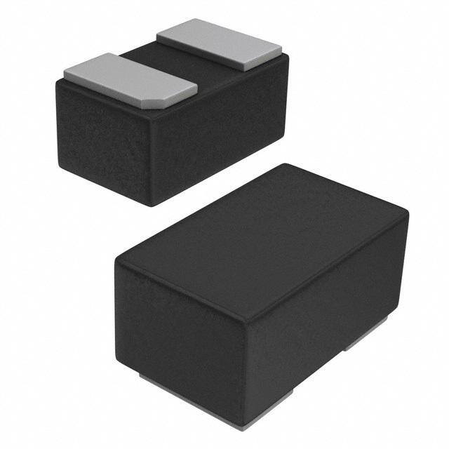
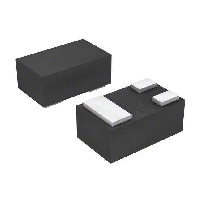
| 描述 | TVS DIODE 5VWM SOD882TVS 二极管 - 瞬态电压抑制器 Single Line Transil Vbr 5V min 26pF 0 |
| 产品分类 | |
| 品牌 | STMicroelectronics |
| 产品手册 | |
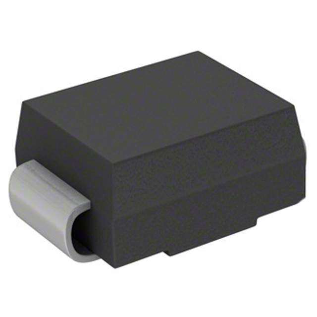
| 产品图片 |
|
| rohs | 符合RoHS无铅 / 符合限制有害物质指令(RoHS)规范要求 |
| 产品系列 | 二极管与整流器,TVS二极管,TVS 二极管 - 瞬态电压抑制器,STMicroelectronics ESDALC5-1BM2ESDA, TRANSIL™ |
| 数据手册 | |
| 产品型号 | ESDALC5-1BM2 |
| 不同频率时的电容 | 26pF @ 1MHz |
| 产品种类 | TVS 二极管 - 瞬态电压抑制器 |
| 供应商器件封装 | SOD-882 |
| 其它名称 | 497-10981-1 |
| 其它有关文件 | http://www.st.com/web/catalog/sense_power/FM114/CL1137/SC1765/PF250155?referrer=70071840http://www.st.com/web/catalog/sense_power/FM114/CL1137/SC492/SS1421/PF250155?referrer=70071840 |
| 击穿电压 | 5 V |
| 功率-峰值脉冲 | 150W |
| 包装 | 剪切带 (CT) |
| 单向通道 | - |
| 双向通道 | 1 |
| 商标 | STMicroelectronics |
| 商标名 | Transil |
| 安装类型 | 表面贴装 |
| 安装风格 | SMD/SMT |
| 封装 | Reel |
| 封装/外壳 | SOD-882 |
| 封装/箱体 | SOD-882 |
| 尺寸 | 1 mm W x 0.6 mm L x 0.4 mm H |
| 峰值浪涌电流 | 9 A |
| 峰值脉冲功率耗散 | 150 W |
| 工作温度 | -55°C ~ 150°C (TJ) |
| 工具箱 | /product-detail/zh/Q7525674/497-8025-KIT-ND/4158069 |
| 工厂包装数量 | 12000 |
| 应用 | 通用 |
| 最大工作温度 | + 150 C |
| 最小工作温度 | - 55 C |
| 极性 | Bidirectional |
| 标准包装 | 1 |
| 电压-击穿(最小值) | 5.8V |
| 电压-反向关态(典型值) | 5V |
| 电压-箝位(最大值)@Ipp | - |
| 电容 | 26 pF |
| 电流-峰值脉冲(10/1000µs) | 9A (8/20µs) |
| 电源线路保护 | 无 |
| 端接类型 | SMD/SMT |
| 类型 | 齐纳 |
| 系列 | ESDALC5-1BM2 |


PDF Datasheet 数据手册内容提取
ESDALC5-1BM2, ESDALC5-1BT2 Single line low capacitance TransilTM, transient surge voltage suppressor (TVS) for ESD protection Datasheet - production data Complies with the following standards IEC 61000-4-2 (exceeds level 4) 30 kV (air discharge) 30 kV (contact discharge) MIL STD 883G - Method 3015-7: class 3 Human body model Description The ESDALC5-1BM2 (SOD882) and ESDALC5-1BT2 (SOD882T) are bidirectional SOD882 SOD882T single-line TVS diodes designed to protect data lines or other I/O ports against ESD transients. These devices are ideal for applications where Features both reduced line capacitance and board space saving are required. Single line low capacitance Transil diode Figure 1: Functional diagram Bidirectional ESD protection Breakdown voltage V = 5.8 V min BR Low diode capacitance (26 pF typ. at 0 V) Low leakage current < 60 nA at 5 V Very small PCB area: 0.6 mm² I/O1 Applications Where transient overvoltage protection in ESD sensitive equipment is required, such as: I/O2 Computers Printers Communication systems Cellular phone handsets and accessories Video equipment TM: Transil is a trademark of Benefits STMicroelectronics High ESD protection level High integration Suitable for high density boards Lead-free packages ECOPACK®2 compliant components November 2016 DocID16936 Rev 6 1/13 This is information on a product in full production. www.st.com
Characteristics ESDALC5-1BM2, ESDALC5-1BT2 1 Characteristics Table 1: Absolute maximum ratings (Tamb = 25 °C) Symbol Parameter Value Unit IEC 61000-4-2: VPP Peak pulse voltage Contact discharge 30 kV Air discharge 30 PPP Peak pulse power 8/20μs, Tj initial = Tamb 150 W IPP Peak pulse current 8/20μs 9 A Tstg Storage temperature range -65 to +150 Tj Junction temperature -55 to +150 °C TL Maximum lead temperature for soldering during 10 s 260 Figure 2: Electrical characteristics (definitions) Table 2: Electrical characteristics (Tamb = 25 °C) Symbol Test condition Min. Typ. Max. Unit From I/O1 to I/O2, IR = 1 mA 11 13 17 VBR V From I/O2 to I/O1, IR = 1 mA 5.8 8 11 IRM VRM = 5 V 60 nA Dynamic resistance, pulse width 100 ns 0.25 Rd From I/O1 to I/O2 0.23 Ω From I/O2 to I/O1 Cline F = 1 MHz, VR = 0 V 26 30 pF 8 kV contact discharge after 30 ns IEC 61000 4-2 16 VCL From I/O1 to I/O2 11 V From I/O2 to I/O1 2/13 DocID16936 Rev 6
ESDALC5-1BM2, ESDALC5-1BT2 Characteristics 1.1 Characteristics (curves) Figure 3: Peak pulse power dissipation versus Figure 4: Leakage current versus junction initial junction temperature (maximum values) temperature (typical values) IR(nA) PPP(W) 1000 250 VR=VRM=5V fromI/O1toI/O2 225 8/20µs 100 200 175 10 150 125 100 1 75 50 0.1 25 Tj(°C) Tj(°C) 0 0.01 0 25 50 75 100 125 150 175 25 50 75 100 125 150 Figure 6: Peak pulse power versus exponential Figure 5: Leakage current versus junction pulse duration (direct) temperature (typical values) 1000 IR(nA) 10000 PPP(W) VR=VRM=5V fromI/O2toI/O1 100 1000 10 100 1 10 0.1 Tj(°C) TP(µs) 0.01 1 25 50 75 100 125 150 1 10 100 1000 Figure 7: Clamping voltage versus peak pulse Figure 8: Clamping voltage versus peak pulse current (typical values) current (typical values) IPP(A) IPP(A) 10 10 8/20µs 8/20µs Tjinitial=25°C Tjinitial=25°C FromI/O1toI/O2 FromI/O2toI/O1 1 1 VCL(V) VCL(V) 0,1 0.1 12 13 14 15 16 17 18 19 20 21 22 23 7 8 9 10 11 12 13 14 15 16 DocID16936 Rev 6 3/13
Characteristics ESDALC5-1BM2, ESDALC5-1BT2 Figure 9: Junction capacitance versus reverse Figure 10: Junction capacitance versus reverse applied voltage (typical values from I/O1 to I/O2) applied voltage (typical values from I/O2 to I/O1) C(pF) C(pF) 35 35 30 froVmoTFsIj/c=O==1123Mt5o0H°ImC/zOV2 30 froVmoTFsIj/c=O==1223Mt5o0H°Im/CzOV1 25 25 20 20 15 15 10 10 5 5 0 VR(V) 0 VR(V) 0 1 2 3 4 5 0 1 2 3 4 5 Figure 11: ESD response to IEC 61000-4-2 Figure 12: ESD response to IEC 61000-4-2 (+8 kV air discharge) (-8 kV air discharge) Figure 13: S21 attenuation measurement result Figure 14: TLP measurement IPP(A) 0 dB 20 18 -5 fromI/O2toI/O1 16 -10 14 -15 12 -20 10 -25 8 -30 6 4 fromI/O1toI/O2 -35 -40 F(Hz) 2 VCL(V) 100k 1M 10M 100M 1G 0 0 5 10 15 20 25 4/13 DocID16936 Rev 6
ESDALC5-1BM2, ESDALC5-1BT2 Package information 2 Package information In order to meet environmental requirements, ST offers these devices in different grades of ECOPACK® packages, depending on their level of environmental compliance. ECOPACK® specifications, grade definitions and product status are available at: www.st.com. ECOPACK® is an ST trademark. 2.1 SOD882 package information Figure 15: SOD882 package outline Table 3: SOD882 package mechanical data Dimensions Ref. Millimeters Inches Min. Typ. Max. Min. Typ. Max. A 0.40 0.47 0.50 0.016 0.019 0.020 A1 0.00 0.05 0.000 0.002 b1 0.45 0.50 0.55 0.018 0.020 0.022 b2 0.45 0.50 0.55 0.018 0.020 0.022 D 0.55 0.60 0.65 0.022 0.024 0.026 E 0.95 1.00 1.05 0.037 0.039 0.041 e 0.60 0.65 0.70 0.024 0.026 0.028 L1 0.20 0.25 0.30 0.008 0.010 0.012 L2 0.20 0.25 0.30 0.008 0.010 0.012 DocID16936 Rev 6 5/13
Package information ESDALC5-1BM2, ESDALC5-1BT2 Figure 16: Footprint recommendations, Figure 17: Marking dimensions in mm (inches) 0.55 0.55 (0.022) (0.022) G 0.50 Pin1 Pin 2 0.020 0.40 (0.016) Product marking may be rotated by multiples of 90° for assembly plant differentiation. In no case should this product marking be used to orient the component for its placement on a PCB. Only pin 1 mark is to be used for this purpose. Figure 18: SOD882 tape and specifications 6/13 DocID16936 Rev 6
ESDALC5-1BM2, ESDALC5-1BT2 Package information 2.2 SOD882T package information Figure 19: SOD882T package outline Table 4: SOD882T package mechanical data Dimensions Ref. Millimeters Inches Min. Typ. Max. Min. Typ. Max. A 0.30 0.40 0.012 0.016 A1 0.00 0.05 0.000 0.002 b1 0.45 0.50 0.55 0.018 0.020 0.022 b2 0.45 0.50 0.55 0.018 0.020 0.022 D 0.55 0.60 0.65 0.022 0.024 0.026 E 0.95 1.00 1.05 0.037 0.039 0.041 e 0.60 0.65 0.70 0.024 0.026 0.028 L1 0.20 0.25 0.30 0.008 0.010 0.012 L2 0.20 0.25 0.30 0.008 0.010 0.012 DocID16936 Rev 6 7/13
Package information ESDALC5-1BM2, ESDALC5-1BT2 Figure 20: Footprint recommendations, Figure 21: Marking dimensions in mm (inches) 0.55 0.55 (0.022) (0.022) H 0.50 Pin1 Pin 2 0.020 0.40 (0.016) Product marking may be rotated by multiples of 90° for assembly plant differentiation. In no case should this product marking be used to orient the component for its placement on a PCB. Only pin 1 mark is to be used for this purpose. Figure 22: SOD882T tape and specifications 8/13 DocID16936 Rev 6
ESDALC5-1BM2, ESDALC5-1BT2 Recommendation on PCB assembly 3 Recommendation on PCB assembly 3.1 Stencil opening design 1. General recommendation on stencil opening design a. Stencil opening dimensions: L (Length), W (Width), T (Thickness). 2. General design rule a. Stencil thickness (T) = 75 ~ 125 μm 𝑊 b. Aspect ratio = ≥1.5 𝑇 𝐿×𝑊 c. Aspect area = ≥0.66 2𝑇(𝐿+𝑊) 3. Reference design a. Stencil opening thickness: 100 μm b. Stencil opening for central exposed pad: Opening to footprint ratio is 50%. c. Stencil opening for leads: Opening to footprint ratio is 90%. Figure 23: Stencil opening dimensions L T W Figure 24: Recommended stencil window position in mm (inches) 3.2 Solder paste 1. Halide-free flux qualification ROL0 according to ANSI/J-STD-004. 2. “No clean” solder paste is recommended. 3. Offers a high tack force to resist component movement during high speed. 4. Solder paste with fine particles: powder particle size is 20-38 μm. DocID16936 Rev 6 9/13
Recommendation on PCB assembly ESDALC5-1BM2, ESDALC5-1BT2 3.3 Placement 1. Manual positioning is not recommended. 2. It is recommended to use the lead recognition capabilities of the placement system, not the outline centering 3. Standard tolerance of ±0.05 mm is recommended. 4. 3.5 N placement force is recommended. Too much placement force can lead to squeezed out solder paste and cause solder joints to short. Too low placement force can lead to insufficient contact between package and solder paste that could cause open solder joints or badly centered packages. 5. To improve the package placement accuracy, a bottom side optical control should be performed with a high resolution tool. 6. For assembly, a perfect supporting of the PCB (all the more on flexible PCB) is recommended during solder paste printing, pick and place and reflow soldering by using optimized tools. 3.4 PCB design preference 1. To control the solder paste amount, the closed via is recommended instead of open vias. 2. The position of tracks and open vias in the solder area should be well balanced. The symmetrical layout is recommended, in case any tilt phenomena caused by asymmetrical solder paste amount due to the solder flow away. 3.5 Reflow profile Figure 25: ST ECOPACK® recommended soldering reflow profile for PCB mounting Minimize air convection currents in the reflow oven to avoid component movement. Maximum soldering profile corresponds to the latest IPC/JEDEC J-STD-020. 10/13 DocID16936 Rev 6
ESDALC5-1BM2, ESDALC5-1BT2 Ordering information 4 Ordering information Figure 26: Ordering information scheme ESDA LC 5 - 1 B x2 ESDarray Lowcapacitance Breakdownvoltage 5= 5.8Voltsmin Numberoflines Directional B=Bi-directional Package M2=SOD882 T2=Thin(SOD882T) Table 5: Ordering information Order code Marking(1) Package Weight Base qty. Delivery mode ESDALC5-1BM2 G SOD882 0.93 mg 12000 Tape and reel ESDALC5-1BT2 H SOD882T 0.82 mg 12000 Tape and reel Notes: (1)The marking can be rotated by multiples of 90° to differentiate assembly location DocID16936 Rev 6 11/13
Revision history ESDALC5-1BM2, ESDALC5-1BT2 5 Revision history Table 6: Document revision history Date Revision Changes 02-Feb-2010 1 Initial release. Updated Figure 11, Figure 12, Figure 15, Figure 19, Table 3, 06-Jun-2012 2 and Table 4. Updated note in page 7, 8 and 13. Updated IRM in Table 2. 05-Mar-2013 3 Clamping voltage at 30 ns added in Table 2. Updated Table 1, Table 2, Table 5, Figure 2, Figure 3, Figure 4, Figure 5, Figure 6, Figure 7, Figure 8, Figure 9, Figure 10, 09-Jan-2014 4 Figure 11, Figure 12, Figure 16, Figure 17, Figure 20, Figure 21 and Figure 24. Added Figure 14. 02-Apr-2014 5 Updated Figure 4 and Figure 5. Updated cover image, Table 2: "Electrical characteristics 28-Nov-2016 6 (Tamb = 25 °C)" and Figure 2: "Electrical characteristics (definitions)". 12/13 DocID16936 Rev 6
ESDALC5-1BM2, ESDALC5-1BT2 IMPORTANT NOTICE – PLEASE READ CAREFULLY STMicroelectronics NV and its subsidiaries (“ST”) reserve the right to make changes, corrections, enhancements, modifications, and improvements to ST products and/or to this document at any time without notice. Purchasers should obtain the latest relevant information on ST products before placing orders. ST products are sold pursuant to ST’s terms and conditions of sale in place at the time of order acknowledgement. Purchasers are solely responsible for the choice, selection, and use of ST products and ST assumes no liability for application assistance or the design of Purchasers’ products. No license, express or implied, to any intellectual property right is granted by ST herein. Resale of ST products with provisions different from the information set forth herein shall void any warranty granted by ST for such product. ST and the ST logo are trademarks of ST. All other product or service names are the property of their respective owners. Information in this document supersedes and replaces information previously supplied in any prior versions of this document. © 2016 STMicroelectronics – All rights reserved DocID16936 Rev 6 13/13