ICGOO在线商城 > 集成电路(IC) > 嵌入式 - 微控制器 - 应用特定 > CY7C53120E4-40SXI
 Datasheet下载
- 型号: CY7C53120E4-40SXI
- 制造商: Cypress Semiconductor
- 库位|库存: xxxx|xxxx
- 要求:
| 数量阶梯 | 香港交货 | 国内含税 |
| +xxxx | $xxxx | ¥xxxx |
查看当月历史价格
查看今年历史价格
CY7C53120E4-40SXI产品简介:
ICGOO电子元器件商城为您提供CY7C53120E4-40SXI由Cypress Semiconductor设计生产,在icgoo商城现货销售,并且可以通过原厂、代理商等渠道进行代购。 CY7C53120E4-40SXI价格参考。Cypress SemiconductorCY7C53120E4-40SXI封装/规格:嵌入式 - 微控制器 - 应用特定, 。您可以下载CY7C53120E4-40SXI参考资料、Datasheet数据手册功能说明书,资料中有CY7C53120E4-40SXI 详细功能的应用电路图电压和使用方法及教程。
Cypress Semiconductor Corp(赛普拉斯半导体公司)生产的CY7C53120E4-40SXI是一款嵌入式微控制器,属于应用特定类别。以下是该型号可能的应用场景:

 1. 工业控制
   - 自动化设备:用于工厂自动化、机器人控制和传感器数据采集系统中,提供高效的数据处理能力。
   - 电机控制:支持复杂的电机驱动算法,适用于家用电器、工业机械等场景。
   - 监控系统:用于环境监测、能源管理或工业过程控制中的实时数据处理。

 2. 消费电子
   - 智能家居设备:如智能灯控、温控器、安防系统等,提供低功耗和高性能的计算能力。
   - 音频/视频设备:用于DVD播放器、音响系统或其他多媒体设备中,支持信号处理和接口控制。
   - 游戏设备:可用于手柄、控制器或其他交互式设备中,实现快速响应和精确控制。

 3. 通信与网络
   - 网络接口设备:如路由器、交换机或网关中的数据包处理模块。
   - 无线通信模块:支持蓝牙、Wi-Fi或其他无线协议的嵌入式系统。
   - 数据传输控制:用于USB桥接、串行通信或其他外设接口的控制。

 4. 汽车电子
   - 车载信息系统:用于导航系统、娱乐系统或信息显示模块。
   - 车身控制系统:如车窗升降、座椅调节、灯光控制等功能。
   - 诊断工具:支持OBD-II或其他车辆诊断协议的嵌入式设备。

 5. 医疗设备
   - 便携式医疗设备:如血糖仪、心率监测仪等,需要低功耗和高可靠性的应用场景。
   - 生命体征监测:用于实时采集和处理生理数据的设备。
   - 小型化仪器:支持紧凑设计和复杂算法的医疗辅助设备。

 6. 物联网(IoT)
   - 传感器节点:用于温度、湿度、压力等传感器数据的采集与传输。
   - 边缘计算设备:在本地进行数据预处理,减少云端负载。
   - 智能仪表:如水表、电表、气表等,支持远程抄表和数据分析。

 特性总结
CY7C53120E4-40SXI具备高性能、低功耗和高度集成的特点,适合需要快速数据处理和复杂控制逻辑的应用场景。其灵活性和可编程性使其能够适应多种行业需求,尤其是在对实时性和可靠性要求较高的环境中表现出色。
| 参数 | 数值 |
| 产品目录 | 集成电路 (IC)半导体 |
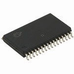
| 描述 | IC PROCESSOR NEURON 32-SOIC网络控制器与处理器 IC Neuron Chip Integ ROM IND |
| 产品分类 | |
| I/O数 | 11 |
| 品牌 | Cypress Semiconductor |
| 产品手册 | |
| 产品图片 |
|
| rohs | 符合RoHS无铅 / 符合限制有害物质指令(RoHS)规范要求 |
| 产品系列 | 通信及网络 IC,网络控制器与处理器 IC,Cypress Semiconductor CY7C53120E4-40SXINeuron® |
| 数据手册 | http://www.cypress.com/?docID=48634 |
| 产品型号 | CY7C53120E4-40SXI |
| PCN组件/产地 | http://www.cypress.com/?docID=47157http://www.cypress.com/?docID=48115 |
| RAM容量 | 2K x 8 |
| 产品 | Network Processor |
| 产品种类 | 网络控制器与处理器 IC |
| 供应商器件封装 | 32-SOIC |
| 其它名称 | CY7C53120E440SXI |
| 包装 | 管件 |
| 商标 | Cypress Semiconductor |
| 安装类型 | 表面贴装 |
| 安装风格 | SMD/SMT |
| 封装 | Tube |
| 封装/外壳 | 32-SOIC(0.455",11.30mm 宽) |
| 封装/箱体 | SOIC-32 |
| 工作温度 | -40°C ~ 85°C |
| 工作电源电压 | 5 V |
| 工厂包装数量 | 25 |
| 应用 | 网络处理器 |
| 接口 | 串行 |
| 控制器系列 | CY7C531xx |
| 最大工作温度 | + 85 C |
| 最小工作温度 | - 40 C |
| 标准包装 | 25 |
| 核心处理器 | 管线 |
| 电压-电源 | 4.5 V ~ 5.5 V |
| 程序存储器类型 | 闪存(4 kB),ROM(12 kB) |
| 系列 | CY7C53120E4 |


- 商务部:美国ITC正式对集成电路等产品启动337调查
- 曝三星4nm工艺存在良率问题 高通将骁龙8 Gen1或转产台积电
- 太阳诱电将投资9.5亿元在常州建新厂生产MLCC 预计2023年完工
- 英特尔发布欧洲新工厂建设计划 深化IDM 2.0 战略
- 台积电先进制程称霸业界 有大客户加持明年业绩稳了
- 达到5530亿美元!SIA预计今年全球半导体销售额将创下新高
- 英特尔拟将自动驾驶子公司Mobileye上市 估值或超500亿美元
- 三星加码芯片和SET,合并消费电子和移动部门,撤换高东真等 CEO
- 三星电子宣布重大人事变动 还合并消费电子和移动部门
- 海关总署:前11个月进口集成电路产品价值2.52万亿元 增长14.8%


PDF Datasheet 数据手册内容提取
CY7C53150, CY7C53120 Neuron Chip Network Processor Features ■Three 8-bit pipelined processors for concurrent processing of ■On-chip LVD circuit to prevent nonvolatile memory corruption application code and network traffic during voltage drops ■11-pin I/O port programmable in 34 modes for fast application ■2,048 bytes of SRAM for buffering network data, system, and program development application data storage ■Two 16-bit timer/counters for measuring and generating I/O ■512 bytes (CY7C53150), 2048 bytes (CY7C53120E2), 4096 device waveforms bytes (CY7C53120E4) of Flash memory with on-chip charge pump for flexible storage of configuration data and application ■5-pin communication port that supports direct connect and code network transceiver interfaces ■Addresses up to 58 KB of external memory (CY7C53150) ■Programmable pull-ups on I/O4–I/O7 and 20 mA sink current on I/O0–I/O3 ■10 KB (CY7C53120E2), 12 KB (CY7C53120E4) of ROM containing LonTalk network protocol firmware ■Unique 48-bit ID number in every device to facilitate network installation and management ■Maximum input clock operation of 20 MHz (CY7C53150), 10MHz (CY7C53120E2), 40 MHz (CY7C53120E4) over a ■Low operating current; sleep mode operation for reduced –40°C to 85°C[2] temperature range current consumption[1] ■64-pin TQFP package (CY7C53150) ■0.35 m flash process technology ■32-pin SOIC or 44-pin TQFP package (CY7C53120) ■5.0 V operation Logic Block Diagram Media Access Communications CP4 Control Processor Port CP0 Network Internal I/O Block I/O10 Processor Data Bus I/O0 (0:7) Application 2 Timer/ Processor Counters Internal Address Bus 2 KB RAM (0:15) CLK1 Oscillator, CLK2 Clock, and Control SERVICE Flash RESET External ROM Address/Data Bus (CY7C53120) (CY7C53150) Notes 1. Rare combinations of wake-up events occurring during the go to sleep sequence could produce unexpected sleep behavior. 2. Maximum Junction Temperature is 105 °C. TJunction = TAmbient + V•I•JA. 32-pin SOIC JA = 51 °C/W. 44-pin TQFP JA = 43 °C/W. 64-pin TQFP JA = 44 °C/W. CypressSemiconductorCorporation • 198 Champion Court • SanJose, CA 95134-1709 • 408-943-2600 Document Number: 38-10001 Rev. *L Revised May 16, 2017
CY7C53150, CY7C53120 Contents Functional Description .....................................................3 External Memory Interface Timing — CY7C53150 .......10 Pin Configurations ...........................................................4 Differential Transceiver Electrical Characteristics ......10 Pin Descriptions ...............................................................6 Ordering Information[23] ...............................................14 Memory Usage ..................................................................7 Ordering Code Definitions .........................................14 Flash Memory Retention and Endurance .......................7 Package Diagrams ..........................................................15 40 MHz 3120 Operation ....................................................7 Acronyms ........................................................................17 Low Voltage Inhibit Operation .........................................7 Document Conventions .................................................17 Communications Port ......................................................7 Units of Measure .......................................................17 Programmable Hysteresis Values ...............................8 Document History Page .................................................18 Programmable Glitch Filter Values[7] ...........................8 Sales, Solutions, and Legal Information ......................19 Receiver[8] (End-to-End) Absolute Asymmetry ...........8 Worldwide Sales and Design Support .......................19 Differential Receiver (End-to-End) Products ....................................................................19 Absolute Symmetry[9, 10] .....................................................8 PSoC® Solutions ......................................................19 Electrical Characteristics .................................................9 Cypress Developer Community .................................19 LVI Trip Point (V ...........................................................9 Technical Support .....................................................19 DD) Document Number: 38-10001 Rev. *L Page 2 of 19
CY7C53150, CY7C53120 Functional Description Services at every layer of the OSI networking reference model are implemented in the LonTalk firmware based protocol stored The CY7C531x0 Neuron chip implements a node for LonWorks in 10-KB ROM (CY7C53120E2), 12-KB ROM (CY7C53120E4), distributed intelligent control networks. It incorporates, on a or off-chip memory (CY7C53150). The firmware also contains 34 single chip, the necessary communication and control functions, preprogrammed I/O drivers, greatly simplifying application both in hardware and firmware, that facilitate the design of a programming. The application program is stored in the Flash LonWorks node. memory (CY7C53120) and/or off-chip memory (CY7C53150), and may be updated by downloading over the network. The CY7C531x0 contains a very flexible 5-pin communication port that can be configured to interface with a wide variety of The CY7C53150 incorporates an external memory interface that media transceivers at a wide range of data rates. The most can address up to 64 KB with 6 KB of the address space mapped common transceiver types are twisted-pair, powerline, RF, IR, internally. LonWorks nodes that require large application fiber-optics, and coaxial. programs can take advantage of this external memory capability. The CY7C531x0 is manufactured using state of the art 0.35 m The CY7C53150 Neuron chip is an exact replacement for the Flash technology, providing to designers the most cost-effective Motorola MC143150Bx and Toshiba TMPN3150B1 devices. The Neuron chip solution. CY7C53120E2 Neuron chip is an exact replacement for the Motorola MC143120E2 device since it contains the same firmware in ROM. Document Number: 38-10001 Rev. *L Page 3 of 19
CY7C53150, CY7C53120 Pin Configurations Figure 1. 64-pin TQFP pinout [4]NC A15 E R/WVDDD0 D1VDD VDDVSSD2D3 D4 D5 D6 D7 48 4746 454443 424140 39 383736 3534 33 NC[4] 49 32 CP4 A14 50 31 CP3 A13 51 30 CP2 A12 52 29 CP1 A11 53 28 CP0 A10 54 27 NC[4] A9 55 26 VDD A8 56 25 VSS A7 57 24 CLK1 CY7C53150-20AI A6 58 23 CLK2 A5 59 22 V DD A4 60 21 V SS A3 61 20 V DD A2 62 19 V SS A1 63 18 NC[4] A0 64 17 SERVICE 1 2 3 4 5 6 7 8 9 10 111213 1415 16 Pin 1 Indicator [3] [4]NC I/O0I/O1 I/O2 I/O3ESET VDDVssVppI/O4 I/O5 I/O6 I/O7 I/O8I/O9 I/O10 R Notes 3. The smaller dimple at the bottom left of the marking indicates pin 1. 4. No Connect (NC) — Must not be used. (These pins may be used for internal testing.) Document Number: 38-10001 Rev. *L Page 4 of 19
CY7C53150, CY7C53120 Pin Configurations (continued) Figure 2. 32-pin SOIC pinout and 44-pin QFP pinout [4]C O7 O8 O9 DD[4]C O10 SS P4 P3 [4]C RESET 1 32 V N I/ I/ I/ V N I/ V C C N DD V 2 31 V DD SS I/O4 3 30 I/O5 3 2 1 0 9 8 7 6 5 4 3 I/O3 4 29 I/O6 3 3 3 3 2 2 2 2 2 2 2 I/O2 5 28 I/O7 NC[4] 34 22 NC[4] I/O1 6 SI 27 I/O8 I/O6 35 21 CP1 I/O0 7 y 26 I/O9 y I/O5 36 20 CP0 SERVVVIVCSpESp 891110 53120Ex- 22225432 VIVC/ODSPSD140 NVVCDS[4DS] 333789 CY7C53120Ex-yyAI 111987 VCNDCPD2[4] DD C VDD 12 Y7 21 CP3 RESET 40 16 VSS VSS 13 C 20 CP1 VDD 41 15 CLK1 CLK2 14 19 CP0 I/O4 42 14 CLK2 CLK1 15 18 V V 16 17 CDPD2 I/O3 43 13 VSS SS NC[4] 44 12 NC[4] 0 1 1 2 3 4 5 6 7 8 9 1 1 PIN 1 INDICATOR [4]NC I/O2 I/O1 I/O0 VICE [4]NC VSS Vpp VDD VDD[4]NC R E S Document Number: 38-10001 Rev. *L Page 5 of 19
CY7C53150, CY7C53120 Pin Descriptions CY7C53150 CY7C53120xx CY7C53120xx Pin Name I/O Pin Function TQFP-64 Pin No. SOIC-32 Pin No. TQFP-44 Pin No. CLK1 Input Oscillator connection or external clock 24 15 15 input. CLK2 Output Oscillator connection. Leave open when 23 14 14 external clock is input to CLK1. Maximum of one external load. RESET I/O (Built-In Reset pin (active LOW). Note The 6 1 40 Pullup) allowable external capacitance connected to the RESET pin is 100–1000 pF. SERVICE I/O (Built-In Service pin (active LOW). Alternates 17 8 5 Configurable between input and output at a 76-Hz rate. Pullup) I/O0–I/O3 I/O Large current-sink capacity (20 mA). 2, 3, 4, 5 7, 6, 5, 4 4, 3, 2, 43 General I/O port. The output of timer/ counter 1 may be routed to I/O0. The output of Timer/Counter 2 may be routed to I/O1. I/O4–I/O7 I/O (Built-In General I/O port. The input to 10, 11, 12, 13 3, 30, 29, 28 42, 36, 35, 32 Configurable Timer/Counter 1 may be derived from one Pullups) of I/O4–I/O7. The input to Timer/Counter 2 may be derived from I/O4. I/O8–I/O1 I/O General I/O port. May be used for serial 14, 15, 16 27, 26, 24 31, 30, 27 0 communication under firmware control. D0–D7 I/O Bidirectional memory data bus. 43, 42, 38, 37, N/A N/A 36, 35, 34, 33 R/W Output Read/write control output for external 45 N/A N/A memory. E Output Enable clock control output for external 46 N/A N/A memory. A0–A15 Output Memory address output port. 64, 63, 62, 61, 60, N/A N/A 59, 58, 57, 56, 55, 54, 53, 52, 51, 50, 47 V Input Power input (5 V nom). All V pins must 7, 20, 22, 26, 2, 11, 12, 9, 10, 19, DD DD be connected together externally. 40, 41, 44 18, 25, 32 29, 38, 41 V Input Power input (0 V, GND). All V pins must 8,19, 21, 25, 39 9, 13, 16, 23, 31 7,13, 16, 26, 37 SS SS be connected together externally. Vpp Input In-circuit test mode control. If Vpp is high 9 10 8 when RESET is asserted, the I/O, address and data buses become Hi-Z. CP0–CP4 Communication Bidirectional port supporting communi- 28, 29, 30, 31, 32 19, 20, 17, 21, 22 20, 21, 18, 24, 25 Network cations in three modes. Interface NC — No connect. Must not be connected on the 1, 18, 27, 48, 49 N/A 1, 6, 11, 12, 17, user’s PC board, since they may be 22, 23, 28, 33, 34, connected internal to the chip. 39, 44 Document Number: 38-10001 Rev. *L Page 6 of 19
CY7C53150, CY7C53120 Memory Usage 40 MHz 3120 Operation All Neuron chips require system firmware to be present when The CY7C53120E4-40 device was designed to run at they are powered up. In the case of the CY7C53120 family, this frequencies up to 40 MHz using an external clock oscillator. It is firmware is preprogrammed in the factory in an on-chip ROM. In important to note that external oscillators may typically take on the case of the CY7C53150, the system firmware must be the order of 5 ms to stabilize after power-up. The Neuron chip present in the first 16 KB of an off-chip nonvolatile memory such must be held in reset until the CLK1 input is stable. With some as Flash, EPROM, EEPROM, or NVRAM. These devices must oscillators, this may require the use of a reset-stretching be programmed in a device programmer before board assembly. Low-Voltage Detection chip/circuit. Check the oscillator vendor’s Because the system firmware implements the network protocol, specification for more information about start-up stabilization it cannot itself be downloaded over the network. times. For the CY7C53120 family, the user application program is Low Voltage Inhibit Operation stored in on-chip Flash memory. It may be programmed using a device programmer before board assembly, or may be The on-chip Low-voltage Inhibit circuit trips the Neuron chip downloaded and updated over the LonTalk network from an whenever the V input is less than 4.1 ± 0.3 V. This feature external network management tool. DD prevents the corruption of nonvolatile memory during voltage For the CY7C53150, the user application program is stored in drops. on-chip Flash Memory and also in off-chip memory. The user program may initially be programmed into the off-chip memory Communications Port device using a device programmer. The Neuron chip includes a versatile 5-pin communications port Flash Memory Retention and Endurance that can be configured in three different ways. In Single-Ended Mode, pin CP0 is used for receiving serial data, pin CP1 for trans- Data and code stored in Flash Memory is guaranteed to be mitting serial data, and pin CP2 enables an external transceiver. retained for at least 10 years for programming temperature range Data is communicated using Differential Manchester encoding. of –25°C to 85°C. In Special Purpose Mode, pin CP0 is used for receiving serial The Flash Memory can typically be written 100,000 times without data, pin CP1 for transmitting serial data, pin CP2 transmits a bit any data loss.[5] An erase/write cycle takes 20 ms. The system clock, and pin CP4 transmits a frame clock for use by an external firmware extends the effective endurance of Flash memory in intelligent transceiver. In this mode, the external transceiver is two ways. If the data being written to a byte of Flash memory is responsible for encoding and decoding the data stream. the same as the data already present in that byte, the firmware In Differential Mode, pins CP0 and CP1 form a differential does not perform the physical write. So for example, an appli- receiver with built-in programmable hysteresis and low pass cation that sets its own address in Flash memory after every filtering. Pins CP2 and CP3 form a differential driver. Serial data reset does not use up any write cycles if the address has not is communicated using Differential Manchester encoding. The changed. In addition, system firmware version 13.1 or higher is following tables describe the communications port when used in able to aggregate writes to eight successive address locations Differential Mode. into a single write for CY7C53120E4 devices. For example, if 4KB of code is downloaded over the network, the firmware would execute only 512 writes rather than 4,096. Note 5. For detailed information about data retention after 100K cycles, see the Cypress qualification report. Document Number: 38-10001 Rev. *L Page 7 of 19
CY7C53150, CY7C53120 Programmable Hysteresis Values Receiver[8] (End-to-End) Absolute Asymmetry (Expressed as differential peak-to-peak voltages in terms of V ) (Worst case across hysteresis) DD Hysteresis[6] V Min V Typ V Max Filter (F) Max (t – t ) Unit hys hys hys PLH PHL 0 0.019 V 0.027 V 0.035 V 0 35 ns DD DD DD 1 0.040 V 0.054 V 0.068 V 1 150 ns DD DD DD 2 0.061 V 0.081 V 0.101 V 2 250 ns DD DD DD 3 0.081 V 0.108 V 0.135 V 3 400 ns DD DD DD 4 0.101 V 0.135 V 0.169 V DD DD DD 5 0.121 V 0.162 V 0.203 V DD DD DD Figure 3. Receiver Input Waveform 6 0.142 V 0.189 V 0.236 V DD DD DD 7 0.162 V 0.216 V 0.270 V DD DD DD CP0 – CP1 V + 200 mV hys Programmable Glitch Filter Values[7] CP0 V /2 (Receiver (end-to-end) filter values expressed as transient pulse DD CP1 suppression times) 3 ns Filter (F) Min Typ Max Unit 0 10 75 140 ns Differential Receiver (End-to-End) Absolute 1 120 410 700 ns Symmetry[9, 10] 2 240 800 1350 ns Filter (F) Hysteresis (H) Max (t – t ) Unit PLH PHL 3 480 1500 2600 ns 0 0 24 ns Notes 6. Hysteresis values are on the condition that the input signal swing is 200 mV greater than the programmed value. 7. Must be disabled if data rate is 1.25 Mbps or greater. 8. Receiver input, VD = VCP0 – VCP1, at least 200 mV greater than hysteresis levels. See Figure3. 9. CPO and CP1 inputs each 0.60 Vp – p, 1.25 MHz sine wave 180° out of phase with each other as shown in Figure10. VDD = 5.00 V ± 5%. 10.tPLH: Time from input switching states from low to high to output switching states. tPHL: Time from input switching states from high to low to output switching states. Document Number: 38-10001 Rev. *L Page 8 of 19
CY7C53150, CY7C53120 Electrical Characteristics (V = 4.5 V–5.5 V) DD Parameter Description Min Typ Max Unit V Input Low Voltage V IL I/O0–I/O10, CP0, CP3, CP4, SERVICE, D0-D7, RESET — — 0.8 CP0, CP1 (Differential) — — Programmable V Input High Voltage V IH I/O0–I/O10, CP0, CP3, CP4, SERVICE, D0-D7, RESET 2.0 — — CP0, CP1 (Differential) Programmable — — V Low-Level Output Voltage V OL I < 20 A — — 0.1 out Standard Outputs (I/O = 1.4 mA)[11] — — 0.4 L High Sink (I/O0–I/O3), SERVICE, RESET (I = 20 mA) — — 0.8 OL High Sink (I/O0–I/O3), SERVICE, RESET (I = 10 mA) — — 0.4 OL Maximum Sink (CP2, CP3) (I = 40 mA) — — 1.0 OL Maximum Sink (CP2, CP3) (I = 15 mA) — — 0.4 OL V High-Level Output Voltage V OH I < 20 A V – 0.1 — — out DD Standard Outputs (I = –1.4 mA)[11] V – 0.4 — — OH DD High Sink (I/O0 – I/O3), SERVICE (I = –1.4 mA) V – 0.4 — — OH DD Maximum Source (CP2, CP3) (I = –40 mA) V – 1.0 — — OH DD Maximum Source (CP2, CP3) (I = –15 mA) V – 0.4 — — OH DD V Hysteresis (Excluding CLK1) 175 — — mV hys I Input Current (Excluding Pull Ups) (V to V )[12] — — ±10 A in SS DD I Pull Up Source Current (V = 0 V, Output = High-Z)[12] 60 — 260 A pu out I Operating Mode Supply Current[13]40-MHz Clock[14] — — 55 mA DD 20-MHz Clock — — 32 10-MHz Clock — — 20 5-MHz Clock — — 12 2.5-MHz Clock — — 8 1.25-MHz Clock — — 7 0.625-MHz Clock[14] — — 3 I Sleep Mode Supply Current[1, 13] — — 100 A DDsleep LVI Trip Point (V ) DD Part Number Min Typ Max Unit CY7C53120E2, CY7C53120E4, and CY7C53150 3.8 4.1 4.4 V Notes 11.Standard outputs are I/O4–I/O10, CP0, CP1, and CP4. (RESET is an open drain input/output. CLK2 must have < 15 pF load.) For CY7C53150, standard outputs also include A0–A15, D0–D7, E, and R/W. 12.I/O4–I/O7 and SERVICE have configurable pull ups. RESET has a permanent pull up. 13.Supply current measurement conditions: VDD = 5 V, all outputs under no-load conditions, all inputs < 0.2 V or (VDD – 0.2 V), configurable pull ups off, crystal oscillator clock input, differential receiver disabled. The differential receiver adds approximately 200 µA typical and 600 µA maximum when enabled. It is enabled on either of the following conditions: Neuron chip in Operating mode and Comm Port in Differential mode. Neuron chip in Sleep mode and Comm Port in Differential mode and Comm Port Wake-up not masked. 14.Supported through an external oscillator only. Document Number: 38-10001 Rev. *L Page 9 of 19
CY7C53150, CY7C53120 External Memory Interface Timing — CY7C53150 V ± 10% (V = 4.5 V to 5.5 V, T = –40 °C to +85 °C [2]) DD DD A Parameter Description Min Max Unit t Memory Cycle Time (System Clock Period)[15] 100 3200 ns cyc PW Pulse Width, E High[16] t /2 – 5 t /2 + 5 ns EH cyc cyc PW Pulse Width, E Low[16] t /2 – 5 t /2 + 5 ns EL cyc cyc t Delay, E High to Address Valid[20] — 35 ns AD t Address Hold Time After E High[20] 10 — ns AH t Delay, E High to R/W Valid Read[20] — 25 ns RD t R/W Hold Time Read After E High 5 — ns RH t Delay, E High to R/W Valid Write — 25 ns WR t R/W Hold Time Write After E High 5 — ns WH t Read Data Setup Time to E High 15 — ns DSR t Data Hold Time Read After E High 0 — ns DHR t Data Hold Time Write After E High[17, 18] 10 — ns DHW t Delay, E Low to Data Valid — 12 ns DDW t Data Three State Hold Time After E Low[19] 0 — ns DHZ t Delay, E High to Data Three-State[18] — 42 ns DDZ t External Memory Access Time (t = t – t – t ) at 50 — ns acc acc cyc AD DSR 20-MHz input clock Differential Transceiver Electrical Characteristics Characteristic Min Max Unit Receiver Common Mode Voltage Range to maintain hysteresis[21] 1.2 V – 2.2 V DD Receiver Common Mode Range to operate with unspecified hysteresis 0.9 V – 1.75 V DD Input Offset Voltage –0.05 V – 35 0.05 V + 35 mV hys hys Propagation Delay (F = 0, V = V /2 + 200 mV) — 230 ns ns ID hys Input Resistance 5 — M Wake-up Time — 10 s Differential Output Impedance for CP2 and CP3[22] 35 Notes 15.tcyc = 2(1/f), where f is the input clock (CLK1) frequency (20, 10, 5, 2.5, 1.25, or 0.625 MHz). 16.Refer to Figure5 for detailed measurement information. 17.The data hold parameter, tDHW, is measured to the disable levels shown in Figure7, rather than to the traditional data invalid levels. 18.Refer to Figure8 and Figure7 for detailed measurement information. 19.The three-state condition is when the device is not actively driving data. Refer to Figure4 and Figure7 for detailed measurement information. 20.To meet the timing above for 20-MHz operation, the loading on A0–A15, D0–D7, and R/W is 30 pF. Loading on E is 20 pF. 21.Common mode voltage is defined as the average value of the waveform at each input at the time switching occurs. 22.Z0 = |V[CP2]-V[CP3] |/40 mA for 4.75 < VDD < 5.25 V. Document Number: 38-10001 Rev. *L Page 10 of 19
CY7C53150, CY7C53120 Figure 4. Signal Loading for Timing Specifications Unless Otherwise Specified TEST SIGNAL C = 20 pF for E L C = 30 pF for A0–A15, D0–D7, and R/W L CL CL = 50 pF for all other signals Figure 5. Test Point Levels for E Pulse Width Measurements PW PW EH EL 2.0 V 2.0 V 0.8 V Figure 6. Drive Levels and Test Point Levels for Timing Specifications Unless Otherwise Specified DRIVE TO 2.4 V 2.0 V 0.8 V DRIVE TO 0.4 V A B 2.0 V 0.8 V A — Signal valid-to-signal valid specification (maximum or minimum) B — Signal valid-to-signal invalid specification (maximum or minimum) Figure 7. Test Point Levels for Driven-to-Three-State Time Measurements V – 0.5 V OH V + 0.5 V OL V – Measured high output drive level OH V – Measured low output drive level OL Figure 8. Signal Loading for Driven-to-Three-State Time Measurements TEST SIGNAL VDD/2 C = 30 pF I = 1.4 mA L LOAD Document Number: 38-10001 Rev. *L Page 11 of 19
CY7C53150, CY7C53120 Figure 9. External Memory Interface Timing Diagram tcyc E PWEH PWEL 20 pF Load Address tAD tAD tAD tAD (A0 – A15) Address Address Address Address 30 pF Load tAH tAH tAH tAH tRD tWR R/W 30 pF Load tRH tWH tDSR tDSR Data (In) Data In Data In (D0 – D7) tDHR tDHR tDDW tDDZ tDDW tDDZ tDHZ tDHW Data (Out) tDHZ tDHW (D0 – D7) Data Out Data Out 30 pF Load Memory READ Memory READ Memory WRITE Memory WRITE Document Number: 38-10001 Rev. *L Page 12 of 19
CY7C53150, CY7C53120 Figure 10. Differential Receiver Input Hysteresis Voltage Measurement Waveforms Voltage 5 4 V(CP0) 3 Vcm V(CP1) 2 V(CP0)-V(CP1) 1 Time Vtrip+ Vh Vtrip- -1 Neuron Chip's 5V Internal Comparator 0V Common-Mode voltage: Vcm = ( V(CP0) + V(CP1) ) / 2 Hysteresis Voltage: Vh = [Vtrip+] - [Vtrip-] Document Number: 38-10001 Rev. *L Page 13 of 19
CY7C53150, CY7C53120 Ordering Information[23] Max Input Flash ROM Firmware Package Part Number Clock Package Type (KB) (KB) Version Name (MHz) CY7C53150-20AXI 0.5 0 N/A 20[24] A64SA 64-pin TQFP CY7C53150-20AXIT 0.5 0 N/A 20[24] A64SA 64-pin TQFP – Tape and Reel CY7C53120E2-10SXI[25] 2 10 6 10 S32.45 32-pin SOIC CY7C53120E4-40SXI[26] 4 12 13 40 S32.45 32-pin SOIC CY7C53120E4-40SXIT 4 12 13 40 S32.45 32-pin SOIC – Tape and Reel CY7C53120E4-40AXI[26] 4 12 13 40 A44 44-pin TQFP Ordering Code Definitions Notes 23.All parts contain 2 KB of SRAM. 24.CY7C53150 may be used with 20-MHz input clock only if the firmware in external memory is version 13 or later. 25.CY7C53120E2 firmware is bit-for-bit identical with Motorola MC143120E2 firmware. 26.CY7C53120E4 requires upgraded LonBuilder® and NodeBuilder® software. Document Number: 38-10001 Rev. *L Page 14 of 19
CY7C53150, CY7C53120 Package Diagrams Figure 11. 44-pin TQFP (10 × 10 × 1.4 mm) Package Outline, 51-85064 51-85064 *G Figure 12. 64-pin TQFP (14 × 14 × 1.4 mm) Package Outline, 51-85046 (cid:537) 1 (cid:537) (cid:537) 2 SYMBOL DIMENSIONS NOTE: MIN.NOM.MAX. 1. JEDEC STD REF MS-026 A 1.60 2. BODY LENGTH DIMENSION DOES NOT A1 0.05 0.15 INCLUDE MOLD PROTRUSION/END FLASH A2 1.35 1.40 1.45 MOLD PROTRUSION/END FLASH SHALL D 15.7516.0016.25 BNOODT YE XLECNEGEDTH 0 .D00IM98E NinS (I0O.2N5S m AmR)E P MEARX S PIDLEASTIC D1 13.9514.0014.05 BODY SIZE INCLUDING MOLD MISMATCH E 15.7516.0016.25 3. DIMENSIONS IN MILLIMETERS E1 13.9514.0014.05 R1 0.08 0.20 R2 0.08 0.20 (cid:537) 0° 7° (cid:537)1 0° (cid:537)2 11° 12° 13° c 0.20 b 0.30 0.35 0.40 L 0.45 0.60 0.75 L1 1.00 REF L2 0.25 BSC L3 0.20 51-85046 *H e 0.80 TYP Document Number: 38-10001 Rev. *L Page 15 of 19
CY7C53150, CY7C53120 Package Diagrams (continued) Figure 13. 32-pin SOIC (450 Mils) Package Outline, 51-85081 51-85081 *E Document Number: 38-10001 Rev. *L Page 16 of 19
CY7C53150, CY7C53120 Acronyms Acronym Description Acronym Description AC Alternating Current LVD Low Voltage Detect CMOS Complementary Metal Oxide Semiconductor PCB Printed Circuit Board DC Direct Current PSoC® Programmable System-on-Chip EEPROM Electrically Erasable Programmable Read-Only SOIC Small-Outline Integrated Circuit Memory GPIO General Purpose I/O TQFP Thin Quad Flat Pack Document Conventions Units of Measure Symbol Unit of Measure Symbol Unit of Measure °C degree Celsius ms millisecond Hz hertz nA nanoampere kHz kilohertz ns nanosecond k kilohm W ohm MHz megahertz % percent µA microampere pF picofarad µs microsecond V volts mA milliampere W watt mm millimeter Document Number: 38-10001 Rev. *L Page 17 of 19
CY7C53150, CY7C53120 Document History Page Document Title: CY7C53150, CY7C53120, Neuron Chip Network Processor Document Number: 38-10001 Orig. of Submission Revision ECN Description of Change Change Date ** 111472 DSG 11/28/01 Change from Spec number: 38-00891 to 38-10001 *A 111990 CFB 02/06/02 Changed the max. cur rent values Specified the Flash endurance of “100K typical” with reference to qual report Fixed some incorrect footnotes and figure numbering *B 114465 KBO 04/24/02 Added Sleep Metastability footnote Added Junction Temperature footnote Added maximum sleep current footnote Changed “EEPROM” references to “Flash Memory” *C 115269 KBO 04/26/02 Repositioned Note 3 *D 124450 KBO 03/25/03 Removed Note 2 regarding data retention Removed Note 16 regarding max sleep current Changed the system image firmware version from V12 to V13.1 *E 837840 BOO 3/14/07 Modified the Ordering Information table; added an “X” to indicate the part numbers are Pb-free; two tape-and-reel options are available now. Implemented new template. *F 2811866 TGE 11/20/2009 Updated template. Modified Note 1 to add reference to the Neuron TRM. *G 2899886 VED 03/26/10 Removed inactive part from the ordering information table. Updated package diagrams. Updated links in Sales, Solutions and Legal Information. *H 3271364 REID / NJF / 06/01/11 Updated Ordering Information table: UVS / PKAR Firmware version for the following parts changed from 12 to 13. CY7C53120E4-40SXI CY7C53120E4-40SXIT CY7C53120E4-40AXI Added Ordering code definitions Added Acronyms, and Units of measure. Revised package diagram specs 51-85064 and 51-85046 to *E. *I 3540297 GNKK 03/02/2012 Sunset review; no content updates. *J 4313266 PMAD 03/20/2014 Updated Features: Updated Note 1. Updated Package Diagrams: spec 51-85064 – Changed revision from *E to *F. spec 51-85046 – Changed revision from *E to *F. spec 51-85081 – Changed revision from *D to *E. Updated in new template. *K 4695030 GRAA 03/20/2015 No content update *L 5704101 AESATMP8 05/16/2017 Updated logo and Copyright. Updated Package Diagrams: spec 51-85064 – Changed revision from *F to *G. spec 51-85046 – Changed revision from *F to *H. Document Number: 38-10001 Rev. *L Page 18 of 19
CY7C53150, CY7C53120 Sales, Solutions, and Legal Information Worldwide Sales and Design Support Cypress maintains a worldwide network of offices, solution centers, manufacturer’s representatives, and distributors. To find the office closest to you, visit us at Cypress Locations. Products PSoC® Solutions ARM® Cortex® Microcontrollers cypress.com/arm PSoC 1 | PSoC 3 | PSoC 4 | PSoC 5LP | PSoC 6 Automotive cypress.com/automotive Cypress Developer Community Clocks & Buffers cypress.com/clocks Forums | WICED IOT Forums | Projects | Video | Blogs | Interface cypress.com/interface Training | Components Internet of Things cypress.com/iot Technical Support Memory cypress.com/memory cypress.com/support Microcontrollers cypress.com/mcu PSoC cypress.com/psoc Power Management ICs cypress.com/pmic Touch Sensing cypress.com/touch USB Controllers cypress.com/usb Wireless Connectivity cypress.com/wireless © Cypress Semiconductor Corporation, 2001-2017. This document is the property of Cypress Semiconductor Corporation and its subsidiaries, including Spansion LLC (“Cypress”). This document, including any software or firmware included or referenced in this document (“Software”), is owned by Cypress under the intellectual property laws and treaties of the United States and other countries worldwide. Cypress reserves all rights under such laws and treaties and does not, except as specifically stated in this paragraph, grant any license under its patents, copyrights, trademarks, or other intellectual property rights. If the Software is not accompanied by a license agreement and you do not otherwise have a written agreement with Cypress governing the use of the Software, then Cypress hereby grants you a personal, non-exclusive, nontransferable license (without the right to sublicense) (1) under its copyright rights in the Software (a) for Software provided in source code form, to modify and reproduce the Software solely for use with Cypress hardware products, only internally within your organization, and (b) to distribute the Software in binary code form externally to end users (either directly or indirectly through resellers and distributors), solely for use on Cypress hardware product units, and (2) under those claims of Cypress's patents that are infringed by the Software (as provided by Cypress, unmodified) to make, use, distribute, and import the Software solely for use with Cypress hardware products. Any other use, reproduction, modification, translation, or compilation of the Software is prohibited. TO THE EXTENT PERMITTED BY APPLICABLE LAW, CYPRESS MAKES NO WARRANTY OF ANY KIND, EXPRESS OR IMPLIED, WITH REGARD TO THIS DOCUMENT OR ANY SOFTWARE OR ACCOMPANYING HARDWARE, INCLUDING, BUT NOT LIMITED TO, THE IMPLIED WARRANTIES OF MERCHANTABILITY AND FITNESS FOR A PARTICULAR PURPOSE. To the extent permitted by applicable law, Cypress reserves the right to make changes to this document without further notice. Cypress does not assume any liability arising out of the application or use of any product or circuit described in this document. Any information provided in this document, including any sample design information or programming code, is provided only for reference purposes. It is the responsibility of the user of this document to properly design, program, and test the functionality and safety of any application made of this information and any resulting product. Cypress products are not designed, intended, or authorized for use as critical components in systems designed or intended for the operation of weapons, weapons systems, nuclear installations, life-support devices or systems, other medical devices or systems (including resuscitation equipment and surgical implants), pollution control or hazardous substances management, or other uses where the failure of the device or system could cause personal injury, death, or property damage (“Unintended Uses”). A critical component is any component of a device or system whose failure to perform can be reasonably expected to cause the failure of the device or system, or to affect its safety or effectiveness. Cypress is not liable, in whole or in part, and you shall and hereby do release Cypress from any claim, damage, or other liability arising from or related to all Unintended Uses of Cypress products. You shall indemnify and hold Cypress harmless from and against all claims, costs, damages, and other liabilities, including claims for personal injury or death, arising from or related to any Unintended Uses of Cypress products. Cypress, the Cypress logo, Spansion, the Spansion logo, and combinations thereof, WICED, PSoC, CapSense, EZ-USB, F-RAM, and Traveo are trademarks or registered trademarks of Cypress in the United States and other countries. For a more complete list of Cypress trademarks, visit cypress.com. Other names and brands may be claimed as property of their respective owners. Document Number: 38-10001 Rev. *L Revised May 16, 2017 Page 19 of 19