ICGOO在线商城 > 集成电路(IC) > 嵌入式 - 微控制器 - 应用特定 > TUSB3410IVF
 Datasheet下载
- 型号: TUSB3410IVF
- 制造商: Texas Instruments
- 库位|库存: xxxx|xxxx
- 要求:
| 数量阶梯 | 香港交货 | 国内含税 |
| +xxxx | $xxxx | ¥xxxx |
查看当月历史价格
查看今年历史价格
TUSB3410IVF产品简介:
ICGOO电子元器件商城为您提供TUSB3410IVF由Texas Instruments设计生产,在icgoo商城现货销售,并且可以通过原厂、代理商等渠道进行代购。 TUSB3410IVF价格参考¥询价-¥询价。Texas InstrumentsTUSB3410IVF封装/规格:嵌入式 - 微控制器 - 应用特定, 。您可以下载TUSB3410IVF参考资料、Datasheet数据手册功能说明书,资料中有TUSB3410IVF 详细功能的应用电路图电压和使用方法及教程。
TUSB3410IVF 是 Texas Instruments(德州仪器)推出的一款 USB 接口桥接控制器芯片,属于嵌入式微控制器中的应用特定型产品。它主要用于将 USB 接口转换为 UART 或 FIFO 接口,实现主机与外设之间的数据通信。

该芯片的典型应用场景包括:

1. USB 转串口通信:常用于工业控制、测量设备、传感器等需要通过 USB 接口与 PC 进行串口通信的场合。
2. 数据采集系统:作为 USB 与外部逻辑电路之间的桥梁,用于采集和传输数据。
3. 开发工具与调试接口:在嵌入式开发中,作为目标板与 PC 之间的调试通道,支持固件下载与调试信息输出。
4. 消费类电子产品:如打印机、扫描仪、POS 机等设备中,用于实现与 PC 的 USB 数据连接。
5. 定制外设控制:可编程配置为通用 FIFO 模式,连接 DSP、MCU 或 FPGA,扩展其 USB 接口能力。

TUSB3410IVF 支持全速 USB 2.0 接口,集成 EEPROM 接口,便于厂商自定义设备标识与配置参数,广泛应用于需要可靠、高效 USB 通信的场景。
| 参数 | 数值 |
| 产品目录 | 集成电路 (IC)半导体 |
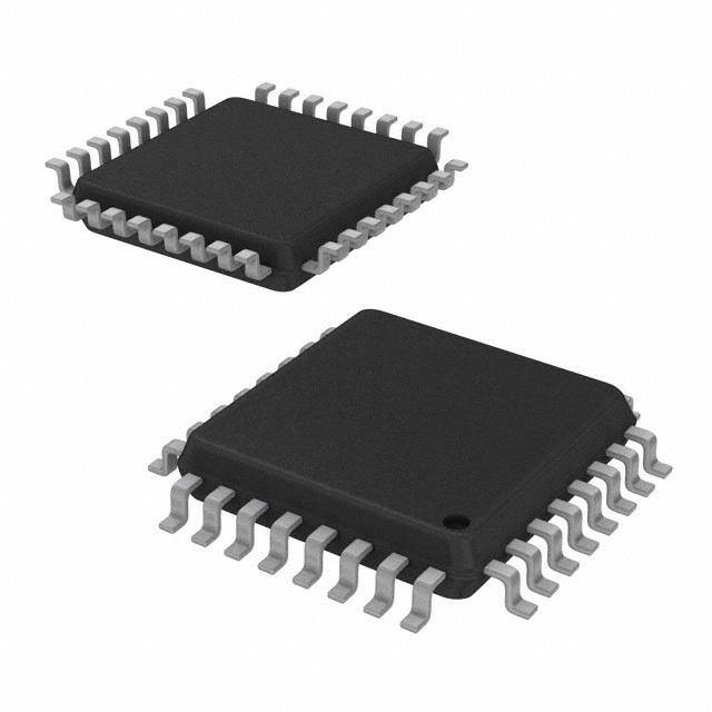
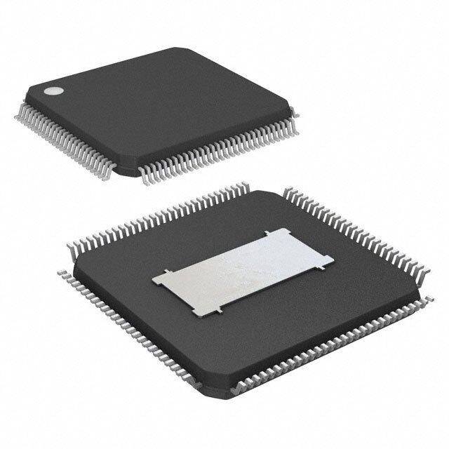
| 描述 | IC CTRLR SERIAL-TO-USB 32-LQFPUSB 接口集成电路 RS232/IrDA Ser-to-USB Converter |
| DevelopmentKit | TUSB3410UARTPDK |
| 产品分类 | |
| I/O数 | 4 |
| 品牌 | Texas Instruments |
| 产品手册 | |
| 产品图片 |
|
| rohs | 符合RoHS无铅 / 符合限制有害物质指令(RoHS)规范要求 |
| 产品系列 | 接口 IC,USB 接口集成电路,Texas Instruments TUSB3410IVFTUSB3410 |
| 数据手册 | |
| 产品型号 | TUSB3410IVF |
| RAM容量 | 18K x 8 |
| 产品培训模块 | http://www.digikey.cn/PTM/IndividualPTM.page?site=cn&lang=zhs&ptm=8124 |
| 产品目录页面 | |
| 产品种类 | USB 接口集成电路 |
| 供应商器件封装 | 32-LQFP(7x7) |
| 其它名称 | 296-16757 |
| 制造商产品页 | http://www.ti.com/general/docs/suppproductinfo.tsp?distId=10&orderablePartNumber=TUSB3410IVF |
| 包装 | 托盘 |
| 单位重量 | 174.300 mg |
| 商标 | Texas Instruments |
| 安装类型 | 表面贴装 |
| 安装风格 | SMD/SMT |
| 封装 | Tray |
| 封装/外壳 | 32-LQFP |
| 封装/箱体 | LQFP-32 |
| 工作温度 | -40°C ~ 85°C |
| 工作电源电压 | 3.3 V |
| 工作电源电流 | 15 mA |
| 工厂包装数量 | 250 |
| 应用 | USB 至串行端口控制器 |
| 接口 | I²C, USB, UART |
| 接口类型 | I2C, UART, USB |
| 控制器系列 | TUSB |
| 数据速率 | 12 Mbps |
| 最大工作温度 | + 85 C |
| 最小工作温度 | - 40 C |
| 标准 | USB 2.0 |
| 标准包装 | 250 |
| 核心处理器 | 8052 |
| 电压-电源 | 3 V ~ 3.6 V |
| 程序存储器类型 | ROM(10 kB) |
| 类型 | Bridge / Converter |
| 系列 | TUSB3410 |
| 速度 | High-Speed |
| 配用 | /product-detail/zh/TUSB3410UARTPDK/296-18080-ND/772111/product-detail/zh/TUSB3410GPIOPDK/TUSB3410GPIOPDK-ND/1910092 |


- 商务部:美国ITC正式对集成电路等产品启动337调查
- 曝三星4nm工艺存在良率问题 高通将骁龙8 Gen1或转产台积电
- 太阳诱电将投资9.5亿元在常州建新厂生产MLCC 预计2023年完工
- 英特尔发布欧洲新工厂建设计划 深化IDM 2.0 战略
- 台积电先进制程称霸业界 有大客户加持明年业绩稳了
- 达到5530亿美元!SIA预计今年全球半导体销售额将创下新高
- 英特尔拟将自动驾驶子公司Mobileye上市 估值或超500亿美元
- 三星加码芯片和SET,合并消费电子和移动部门,撤换高东真等 CEO
- 三星电子宣布重大人事变动 还合并消费电子和移动部门
- 海关总署:前11个月进口集成电路产品价值2.52万亿元 增长14.8%


PDF Datasheet 数据手册内容提取
Product Order Technical Tools & Support & Reference Folder Now Documents Software Community Design TUSB3410,TUSB3410I SLLS519J–MARCH2002–REVISEDJULY2017 TUSB3410 USB to Serial Port Controller 1 Device Overview • EnhancedUARTFeatures: 1.1 Features – SoftwareandHardwareFlowControl • FullyCompliantWithUSB2.0Full-Speed – AutomaticRS-485BusTransceiverControl, 1 Specifications:TID#40340262 WithandWithoutEcho • Supports12-MbpsUSBDataRate(FullSpeed) – SelectableIrDAModeforUpto115.2-kbps • SupportsUSBSuspend,Resume,andRemote Transfer Wake-UpOperations – Software-SelectableBaudRateFrom50BPSto • ConfigurabletoBus-PoweredandSelf-Powered 921.6kbps Operation – ProgrammableSerial-InterfaceCharacteristics • SupportsaTotalofThreeInputandThreeOutput – 5-,6-,7-,or8-BitCharacters (Interrupt,Bulk)Endpoints – Even,Odd,orNoParity-bitGenerationand • Integrated8052MicrocontrollerWith: Detection – 256 ×8RAMforInternalData – 1-,1.5-,or2-StopBitGeneration – 10K ×8ROM(WithUSBandI2CBootloader) – LineBreakGenerationandDetection – 16K ×8RAMforCodeSpaceLoadableFrom – InternalTestandLoopbackCapabilities HostorI2CPort – ModemControlFunctions(CTS,RTS,DSR,RI – 2K× 8SharedRAMUsedforDataBuffersand andDCD) EndpointDescriptorBlocks(EDBs) – InternalDiagnosticCapability – MasterI2CControllerforEEPROMDevice – LoopbackControlforCommunications Access Link-FaultIsolation – MCUOperatesat24MHz,Providing2-MIPS – Break,Parity,Overrun,Framing-Error Operation Simulation – 128-msWatchdogTimer 1.2 Applications • Modems • MedicalMeters • Peripherals: • DSPandµCInterface Printers,HandheldDevices,andsoon 1.3 Description The TUSB3410 device provides bridging between a USB port and an enhanced UART serial port. The devicecontainsan8052microcontrollerunit(MCU)with16KBofRAMthatcanbeloadedfromthehostor from the external onboard memory through an I2C. The device also contains 10KB of ROM that allows the MCU to configure the USB port at boot time. The ROM code also contains an I2C bootloader. All device functions (such as the USB command decoding, UART setup, and error reporting) are managed by the internalMCUfirmwareinunisonwiththePChost. DeviceInformation PARTNUMBER PACKAGE BODYSIZE VQFN(32) 5.00mm×5.00mm TUSB3410 LQFP(32) 7.00mm×7.00mm 1. Forallavailablepackages,seetheorderableaddendumattheendofthedatasheet. 1 An IMPORTANT NOTICE at the end of this data sheet addresses availability, warranty, changes, use in safety-critical applications, intellectualpropertymattersandotherimportantdisclaimers.PRODUCTIONDATA.
TUSB3410,TUSB3410I SLLS519J–MARCH2002–REVISEDJULY2017 www.ti.com 1.4 Functional Block Diagram 12MHz Clock Oscillator 8052 PLLand 24MHz Core Dividers 8 8 10K×8 2×16-Bit USB ROM Timers TxR DP,DM 8 16K×8 8 4 P3.4 RAM P3.3 Port3 P3.1 8 P3.0 2K×8 SRAM 8 I2C I2CBus Controller 8 DMA-1 8 CPU-I/F DMA-3 Suspend/ Resume USB Serial 8 RTS Interface 8 8 UART−1 CTS Engine UBM DTR USBBuffer DSR Manager SIN SOUT TDM Control Logic IR Encoder M U SOUT/IR_SOUT X IR SIN/IR_SIN M Decoder U X Copyright©2017,TexasInstrumentsIncorporated 2 DeviceOverview Copyright©2002–2017,TexasInstrumentsIncorporated SubmitDocumentationFeedback ProductFolderLinks:TUSB3410
TUSB3410,TUSB3410I www.ti.com SLLS519J–MARCH2002–REVISEDJULY2017 Table of Contents 1 DeviceOverview......................................... 1 5.5 Memory.............................................. 24 .............................................. .......................................... 1.1 Features 1 5.6 BootModes 67 1.2 Applications........................................... 1 6 Application,Implementation,andLayout......... 84 ............................................ .............................. 1.3 Description 1 6.1 ApplicationInformation 84 ............................ .................................. 1.4 FunctionalBlockDiagram 2 6.2 TypicalApplication 84 2 Revision History......................................... 3 6.3 Layout............................................... 88 3 PinConfigurationandFunctions..................... 4 6.4 PowerSupplyRecommendations .................. 90 ......................................... .................................... 3.1 PinDiagrams 4 6.5 CrystalSelection 90 4 Specifications ............................................ 6 6.6 ExternalCircuitRequiredforReliableBusPowered ................................. .......................... Suspend Operation 91 4.1 AbsoluteMaximumRatings 6 .......................................... 7 DeviceandDocumentationSupport............... 92 4.2 ESDRatings 6 ............................. ................ 7.1 DocumentationSupport 92 4.3 RecommendedOperatingConditions 6 ........................................ .................................. 7.2 RelatedLinks 92 4.4 Thermal Information 6 .. ............................. 7.3 ReceivingNotificationofDocumentationUpdates 92 4.5 ElectricalCharacteristics 7 .............................. .... 7.4 CommunityResources 92 4.6 TimingandSwitchingCharacteristicsInformation 8 .......................................... ............................... 7.5 Trademarks 92 4.7 Typical Characteristics 9 ..................... 5 DetailedDescription .................................. 10 7.6 ElectrostaticDischargeCaution 92 ............................................. ............................................ 7.7 Glossary 92 5.1 Overview 10 ........................... 8 MechanicalPackagingandOrderable 5.2 FunctionalBlockDiagram 11 Information.............................................. 93 ........................... 5.3 DeviceFunctionalModes 11 .............................. .............................. 8.1 PackagingInformation 93 5.4 ProcessorSubsystems 16 2 Revision History NOTE:Pagenumbersforpreviousrevisionsmaydifferfrompagenumbersinthecurrentversion. ChangesfromRevisionI(November2015)toRevisionJ Page • Changedpin21From:DTRTo:activelowDTRinthePinFunctionstable.................................................. 5 • Changedthedescriptionofbit7CONTinUSBCTL:USBControlRegister(Addr:FFFCh),CONT=0From: enabledTo:disables,CONT=1From:disbaledTo:enabled................................................................. 40 ChangesfromRevisionH(April2013)toRevisionI Page • AddedPinConfigurationandFunctionssection,ESDRatingstable,ThermalInformationtable,Typical Characteristicssection,FeatureDescriptionsection,DeviceFunctionalModes,ApplicationandImplementation section,PowerSupplyRecommendationssection,Layoutsection,DeviceandDocumentationSupportsection, andMechanical,Packaging,andOrderableInformationsection .............................................................. 1 • DeletedOrderingInformationtable................................................................................................. 1 Copyright©2002–2017,TexasInstrumentsIncorporated RevisionHistory 3 SubmitDocumentationFeedback ProductFolderLinks:TUSB3410
TUSB3410,TUSB3410I SLLS519J–MARCH2002–REVISEDJULY2017 www.ti.com 3 Pin Configuration and Functions 3.1 Pin Diagrams RHBPackage 32-PinVQFN TopView VFPackage 32-PinLQFP BottomView 4 PinConfigurationandFunctions Copyright©2002–2017,TexasInstrumentsIncorporated SubmitDocumentationFeedback ProductFolderLinks:TUSB3410
TUSB3410,TUSB3410I www.ti.com SLLS519J–MARCH2002–REVISEDJULY2017 PinFunctions PIN I/O DESCRIPTION NAME NO. Clockoutput(controlledbybits2(CLKOUTEN)and3(CLKSLCT)intheMODECNFGregister(see(1)and CLKOUT 22 O Section5.5.5.5) CTS 13 I UART:Cleartosend(2) DCD 15 I UART:Datacarrierdetect(2) DM 7 I/O UpstreamUSBportdifferentialdataminus DP 6 I/O UpstreamUSBportdifferentialdataplus DSR 14 I UART:Datasetready(2) DTR 21 O UART:Dataterminalready(1) GND 8,18,28 GND Digitalground P3.0 32 I/O General-purposeI/O0(port3,terminal0)(3)(4)(5) P3.1 31 I/O General-purposeI/O1(port3,terminal1)(3)(4)(5) P3.3 30 I/O General-purposeI/O3(port3,terminal3)(3)(4)(5) P3.4 29 I/O General-purposeI/O4(port3,terminal4)(3)(4)(5) PUR 5 O Pullupresistorconnection(6) RESET 9 I Devicemasterresetinput(2) RI/CP 16 I UART:Ringindicator(2) RTS 20 O UART:Requesttosend(1) SCL 11 O MasterI2Ccontroller:clocksignal(1) SDA 10 I/O MasterI2Ccontroller:datasignal(1)(4) SIN/IR_SIN 17 I UART:Serialinputdata/IRSerialdatainput(7) SOUT/IR_SOUT 19 O UART:Serialoutputdata/IRSerialdataoutput(8) SUSPEND 2 O Suspendindicatorterminal(3).Whenthisterminalisassertedhigh,thedeviceisinsuspendmode. TEST0 23 I Testinput(forfactorytestonly).ThisterminalmustbetiedtoVCCthrougha10-kΩresistor. TEST1 24 I Testinput(forfactorytestonly)(4).ThisterminalmustbetiedtoVCCthrougha10-kΩresistor. VCC 3,25 PWR 3.3V 1.8-Vsupply.AninternalvoltageregulatorgeneratesthissupplyvoltagewhenterminalVREGENislow.When VDD18 4 PWR VREGENishigh,1.8Vmustbesuppliedexternally. VREGEN 1 I Thisactive-lowterminalisusedtoenablethe3.3-Vto1.8-Vvoltageregulator. WAKEUP 12 I Remotewake-uprequestterminal.Whenlow,wakesupsystem(4) X1/CLKI 27 I 12-MHzcrystalinputorclockinput X2 26 O 12-MHzcrystaloutput (1) 3-stateCMOSoutput(±4-mAdriveandsink) (2) TTL-compatible,hysteresisinput (3) 3-stateCMOSoutput(±12-mAdriveandsink) (4) TTL-compatible,hysteresisinput,withinternal100-µAactivepullupresistor (5) TheMCUtreatstheoutputsasopendraintypesinthattheoutputcanbedrivenlowcontinuously,butahighoutputisdrivenfortwo clockcyclesandthentheoutputishighimpedance. (6) 3-stateCMOSoutput(±8-mAdriveandsink) (7) TTL-compatibleinputwithouthysteresis,withinternal100-µAactivepullupresistor (8) NormalorIRmode:3-stateCMOSoutput(±4-mAdriveandsink) Copyright©2002–2017,TexasInstrumentsIncorporated PinConfigurationandFunctions 5 SubmitDocumentationFeedback ProductFolderLinks:TUSB3410
TUSB3410,TUSB3410I SLLS519J–MARCH2002–REVISEDJULY2017 www.ti.com 4 Specifications 4.1 Absolute Maximum Ratings overoperatingfree-airtemperaturerange(unlessotherwisenoted)(1) MIN MAX UNIT V Supplyvoltage −0.5 3.6 V CC V Inputvoltage −0.5 V +0.5 V I CC V Outputvoltage −0.5 V +0.5 V O CC I Inputclampcurrent ±20 mA IK I Outputclampcurrent ±20 mA OK Industrial –65 150 T Storagetemperature °C stg Standard –55 150 (1) StressesbeyondthoselistedunderAbsoluteMaximumRatingsmaycausepermanentdamagetothedevice.Thesearestressratings only,andfunctionaloperationofthedeviceattheseoranyotherconditionsbeyondthoseindicatedunderRecommendedOperating Conditionsisnotimplied.Exposuretoabsolute-maximum-ratedconditionsforextendedperiodsmayaffectdevicereliability. 4.2 ESD Ratings VALUE UNIT HumanBodyModel(HBM),perANSI/ESDA/JEDECJS001(1) ±2000 V Electrostaticdischarge(ESD) VESD performance CpehraJrgEeSdDD22e-vCic1e0M1(o2d)el(CDM), Allpins ±500 V (1) JEDECdocumentJEP155statesthat500-VHBMallowssafemanufacturingwithastandardESDcontrolprocess. (2) JEDECdocumentJEP157statesthat250-VCDMallowssafemanufacturingwithastandardESDcontrolprocess. 4.3 Recommended Operating Conditions MIN TYP MAX UNIT V Supplyvoltage 3 3.3 3.6 V CC V Inputvoltage 0 V V I CC TTL 2 V CC V High-levelinputvoltage V IH CMOS 0.7×V V CC CC TTL 0 0.8 V Low-levelinputvoltage V IL CMOS 0 0.2×V CC Commercialrange 0 70 °C T Operatingtemperature A Industrialrange –40 85 °C 4.4 Thermal Information TUSB3410 THERMALMETRIC(1) RHB(VQFN) VF(LQFP) UNIT 32PINS R Junction-to-ambientthermalresistance 32.1 70.5 °C/W θJA R Junction-to-case(top)thermalresistance 24.6 31.4 °C/W θJC(top) R Junction-to-boardthermalresistance 6.5 28.3 °C/W θJB ψ Junction-to-topcharacterizationparameter 0.2 2.2 °C/W JT ψ Junction-to-boardcharacterizationparameter 6.5 28.2 °C/W JB R Junction-to-case(bottom)thermalresistance 24.6 31.4 °C/W θJC(bot) (1) Formoreinformationabouttraditionalandnewthermalmetrics,seetheSemiconductorandCPackageThermalMetricsapplication report. 6 Specifications Copyright©2002–2017,TexasInstrumentsIncorporated SubmitDocumentationFeedback ProductFolderLinks:TUSB3410
TUSB3410,TUSB3410I www.ti.com SLLS519J–MARCH2002–REVISEDJULY2017 4.5 Electrical Characteristics T =25°C,V =3.3V±5%,V =0V A CC SS PARAMETER TESTCONDITIONS MIN TYP MAX UNIT TTL V –0.5 CC V High-leveloutputvoltage I =–4mA V OH OH CMOS V –0.5 CC TTL 0.5 V Low-leveloutputvoltage I =4mA V OL OL CMOS 0.5 TTL 1.8 V Positivethresholdvoltage V =V V IT+ I IH CMOS 0.7×V CC TTL 0.8 1.8 V Negativethresholdvoltage V =V V IT− I IH CMOS 0.2×V CC TTL 0.3 0.7 V Hysteresis(V −V ) V =V V hys IT+ IT− I IH CMOS 0.17×V 0.3×V CC CC TTL ±20 I High-levelinputcurrent V =V µA IH I IH CMOS ±1 TTL ±20 I Low-levelinputcurrent V =V µA IL I IL CMOS ±1 I Outputleakagecurrent(Hi-Z) V =V orV ±20 µA OZ I CC SS I Outputlowdrivecurrent 0.1 mA OL I Outputhighdrivecurrent 0.1 mA OH Supplycurrent(operating) Serialdataat921.6k 15 mA I CC Supplycurrent(suspended) 200 µA Clockdutycycle(1) 50% Jitterspecification(1) ±100 ppm C Inputcapacitance 18 pF I C Outputcapacitance 10 pF O (1) Appliestoallclockoutputs Copyright©2002–2017,TexasInstrumentsIncorporated Specifications 7 SubmitDocumentationFeedback ProductFolderLinks:TUSB3410
TUSB3410,TUSB3410I SLLS519J–MARCH2002–REVISEDJULY2017 www.ti.com 4.6 Timing and Switching Characteristics Information 4.6.1 Wakeup Timing (WAKEUP or RI/CP Transitions) The TUSB3410 device can be brought out of the suspended state, or woken up, by a command from the host. The TUSB3410 device also supports remote wakeup and can be awakened by either of two input signals. A low pulse on the WAKEUP terminal or a low-to-high transition on the RI/CP terminal wakes up thedevice. NOTE For reliable operation, either condition must persist for approximately 3-ms minimum, which allowstimeforthecrystalto power up becauseinthesuspendmode,thecrystalinterface is powereddown.The stateof theWAKEUP orRI/CP terminalis then sampledbytheclockto verifytherewasavalidwake-upevent. 4.6.2 Reset Timing There are three requirements for the reset signal timing. First, the minimum reset pulse duration is 100 μs. At power up, this time is measured from the time the power ramps up to 90% of the nominal V until the CC resetsignalexceeds1.2V.Thesecondrequirementisthattheclockmustbevalidduringthelast60 µsof the reset window. The third requirement is that, according to the USB specification, the device must be ready to respond to the host within 100 ms. This means that within the 100-ms window, the device must come out of reset, load any pertinent data from the I2C EEPROM device, and transfer execution to the application firmware if any is present. Because the latter two events can require significant time, the amount of which can change from system to system, TI recommends having the device come out of reset within 30 ms, leaving 70 ms for the other events to complete. This means the reset signal must rise to 1.8Vwithin30ms. These requirements are depicted in Figure 4-1. When using a 12-MHz crystal, the clock signal may take several milliseconds to ramp up and become valid after power up. Therefore, the reset window may need tobeelongatedupto10msormoretoensurethatthereisa60-µsoverlapwithavalidclock. 3.3V VCC CLK 90% 1.8V RESET 1.2V 0 V t >60μs 100μs<RESETTIME RESETTIME<30ms Figure4-1.ResetTiming 8 Specifications Copyright©2002–2017,TexasInstrumentsIncorporated SubmitDocumentationFeedback ProductFolderLinks:TUSB3410
TUSB3410,TUSB3410I www.ti.com SLLS519J–MARCH2002–REVISEDJULY2017 4.7 Typical Characteristics 8.94 9.8 8.92 3 V 9.79 3.3 V 9.78 8.9 9.77 8.88 9.76 Supply Current (mA) 8888....87888.82468 Supply Current (mA) 999999......9677777.9123457 8.76 9.68 8.74 9.67 9.66 8.72 9.65 8.7 9.64 2400 4800 7200 9600 19200 38400 57600 115200 230400 460800 921600 2400 4800 7200 9600 19200 38400 57600 115200 230400 460800 921600 Baud Rate (bps) Baud Rate (bps) C004 C005 Figure4-2.SupplyCurrentat3V Figure4-3.SupplyCurrentat3.3V 10.64 10.63 3.6 V 10.62 10.61 10.6 mA) 1100..5589 Supply Current (1111100000.....5555534567 10.52 10.51 10.5 10.49 10.48 2400 4800 7200 9600 19200 38400 57600 115200 230400 460800 921600 Baud Rate (bps) C006 Figure4-4.SupplyCurrentat3.6V Copyright©2002–2017,TexasInstrumentsIncorporated Specifications 9 SubmitDocumentationFeedback ProductFolderLinks:TUSB3410
TUSB3410,TUSB3410I SLLS519J–MARCH2002–REVISEDJULY2017 www.ti.com 5 Detailed Description 5.1 Overview The TUSB3410 device provides bridging between a USB port and an enhanced UART serial port. The TUSB3410 device contains all the necessary logic to communicate with the host computer using the USB bus. It contains an 8052 microcontroller unit (MCU) with 16K bytes of RAM that can be loaded from the host or from the external on-board memory through an I2C bus. It also contains 10K bytes of ROM that allow the MCU to configure the USB port at boot time. The ROM code also contains an I2C bootloader. All device functions, such as the USB command decoding, UART setup, and error reporting, are managed by theinternalMCUfirmwareundertheauspicesofthePChost. The TUSB3410 device can be used to build an interface between a legacy serial peripheral device and a PC with USB ports, such as a legacy-free PC. When configured, data flows from the host to the TUSB3410 device through USB OUT commands and then out from the TUSB3410 device on the SOUT line. Conversely, data flows into the TUSB3410 device on the SIN line and then into the host through USB INcommands. Out SOUT Legacy Host USB TUSB3410 Serial (PCorOn-The-Go Peripheral Dual-RoleDevice) In SIN Figure5-1.DataFlow 10 DetailedDescription Copyright©2002–2017,TexasInstrumentsIncorporated SubmitDocumentationFeedback ProductFolderLinks:TUSB3410
TUSB3410,TUSB3410I www.ti.com SLLS519J–MARCH2002–REVISEDJULY2017 5.2 Functional Block Diagram 12MHz Clock Oscillator 8052 PLLand 24MHz Core Dividers 8 8 USB 10K×8 2×16-Bit TxR ROM Timers DP,DM 8 16K×8 8 4 P3.4 RAM Port3 P3.3 P3.1 8 P3.0 2K×8 SRAM 8 I2C I2CBus Controller 8 DMA-1 CPU-I/F 8 DMA-3 Suspend/ USB Resume Serial 8 RTS InEtnegrfiancee 8 UBM 8 UART−1 CDTTSR USBBuffer DSR Manager SIN SOUT TDM Control Logic IR Encoder M U SOUT/IR_SOUT X IR M Decoder SIN/IR_SIN U X Copyright©2017,TexasInstrumentsIncorporated Figure5-2.USB-to-Serial(SingleChannel)ControllerBlockDiagram 5.3 Device Functional Modes The TUSB3410 device controls its USB interface in response to USB commands, and this action is independent of the serial port mode selected. On the other hand, the serial port can be configured in three differentmodes. As with any interface device, data movement is the main function of the TUSB3410 device, but typically the initial configuration and error handling consume most of the support code. The following sections describethevariousmodesthedevicecanbeusedinandthemeansofconfiguringthedevice. 5.3.1 USB Interface Configuration The TUSB3410 device contains onboard ROM microcode, which enables the MCU to enumerate the device as a USB peripheral. The ROM microcode can also load application code into internal RAM from eitherexternalmemorythroughtheI2CbusorfromthehostthroughtheUSB. Copyright©2002–2017,TexasInstrumentsIncorporated DetailedDescription 11 SubmitDocumentationFeedback ProductFolderLinks:TUSB3410
TUSB3410,TUSB3410I SLLS519J–MARCH2002–REVISEDJULY2017 www.ti.com 5.3.1.1 ExternalMemoryCase After reset, the TUSB3410 device is disconnected from the USB. Bit 7 (CONT) in the USBCTL register (seeSection5.5.5.4)iscleared.TheTUSB3410devicecheckstheI2Cportfortheexistenceofvalidcode; if it finds valid code, then the device uploads the code from the external memory device into the RAM program space. When loaded, the TUSB3410 device connects to the USB by setting the CONT bit; then, enumerationandconfigurationareperformed.Thisisthemostlikelyuseofthedevice. 5.3.1.2 HostDownloadCase If the valid code is not found at the I2C port, then the TUSB3410 device connects to the USB by setting bit 7 (CONT) in the USBCTL register (see Section 5.5.5.4), and then an enumeration and default configuration are performed. The host can download additional microcode into RAM to tailor the application. Then, the MCU causes a disconnect and reconnect by clearing and setting the CONT bit, whichcausestheTUSB3410devicetobere-enumeratedwithanewconfiguration. 5.3.2 USB Data Movement From the USB perspective, the TUSB3410 device looks like a USB peripheral device. It uses endpoint zeroasitscontrolendpoint,asdoallUSBperipherals.Italsoconfiguresuptothreeinputandthreeoutput endpoints,althoughmostapplicationsuseonebulkinputendpointfordatain,onebulkoutputendpointfor data out, and one interrupt endpoint for status updates. The USB configuration likely remains the same regardlessoftheserialportconfiguration. Most data is moved from the USB side to the UART side and from the UART side to the USB side using on-chipDMAtransfers.SomespecialcasesmayuseprogrammedI/OundercontroloftheMCU. 5.3.3 Serial Port Setup The serial port requires a few control registers to be written to configure its operation. This configuration likelyremainsthesameregardlessofthedatamodeused.Theseregistersincludethelinecontrolregister thatcontrolstheserialwordformatandthedivisorregistersthatcontrolthebaudrate. Theseregistersareusuallycontrolledbythehostapplication. 5.3.4 Serial Port Data Modes The serial port can be configured in three different, although similar, data modes: the RS-232 data mode, the RS-485 data mode, and the IrDA data mode. Similar to the USB mode, when configured for a specific application, it is unlikely that the mode would be changed. The different modes affect the timing of the serial input and output or the use of the control signals. However, the basic serial-to-parallel conversion of the receiver and parallel-to-serial conversion of the transmitter remain the same in all modes. Some features are available in all modes, but are only applicable in certain modes. For instance, software flow control through Xoff/Xon characters can be used in all modes, but would usually only be used in RS-232 or IrDA mode because the RS-485 mode is half-duplex communication. Similarly, hardware flow control through RTS/CTS (or DTR/DSR) handshaking is available in RS-232 or IrDA mode. However, this would probably be used only in RS-232 mode, because in IrDA mode only the SIN and SOUT paths are optically coupled. 5.3.4.1 RS-232DataMode The default mode is called the RS-232 mode and is typically used for full duplex communication on SOUT and SIN. In this mode, the modem control outputs (RTS and DTR) communicate to a modem or are general outputs. The modem control inputs (CTS, DSR, DCD, and RI/CP) communicate to a modem or aregeneralinputs.Alternatively, RTS andCTS (orDTRandDSR)canthrottlethedataflowonSOUTand SIN to prevent receive FIFO overruns. Finally, software flow control through Xoff/Xon characters can be usedforthesamepurpose(seeSection5.2). This mode represents the most general-purpose applications, and the other modes are subsets of this mode. 12 DetailedDescription Copyright©2002–2017,TexasInstrumentsIncorporated SubmitDocumentationFeedback ProductFolderLinks:TUSB3410
TUSB3410,TUSB3410I www.ti.com SLLS519J–MARCH2002–REVISEDJULY2017 5.3.4.2 RS-485DataMode TheRS-485modeisverysimilartotheRS-232modeinthattheSOUTandSINformatsremainthesame. Because RS-485 is a bus architecture, it is inherently a single duplex communication system. The TUSB3410 device in RS-485 mode controls the RTS and DTR signals such that either can enable an RS- 485 driver or RS-485 receiver. When in RS-485 mode, the enable signals for transmitting are automaticallyassertedwhenevertheDMAissetupforoutbounddata. NOTE The receiver can be left enabled while the driver is enabled to allow an echo if desired, but when receive data is expected, the driver must be disabled. This precludes use of hardware flow control, because this is a half-duplex operation, it would not be effective. Software flow controlissupported,butmaybeoflimitedvalue. The RS-485 mode is enabled by setting bit 7 (485E) in the FCRL register (see Section 5.5.7.4), and bit 1 (RCVE) in the MCR register (see Section 5.5.7.6) allows the receiver to eavesdrop while in the RS-485 mode. 5.3.4.3 IrDADataMode The IrDA mode encodes SOUT and decodes SIN in the manner prescribed by the IrDA standard, up to 115.2 kbps. Connection to an external IrDA transceiver is required. Communications is usually full duplex. Generally, in an IrDA system, only the SOUT and SIN paths are connected so hardware flow control is usuallynotanoption.Softwareflowcontrolissupported(seeSection5.2). TheIrDAmodeisenabledbysettingbit6(IREN)intheUSBCTLregister(seeSection5.5.5.4). The IR encoder and decoder circuitry work with the UART to change the serial bit stream into a series of pulses and back again. For every zero bit in the outbound serial stream, the encoder sends a low-to-high- to-low pulse with the duration of 3/16 of a bit frame at the middle of the bit time. For every one bit in the serialstream,theoutputremainslowfortheentirebittime. ThedecodingprocessconsistsofreceivingthesignalfromtheIrDAreceiverandconvertingitintoaseries of zeroes and ones. As the converse to the encoder, the decoder converts a pulse to a zero bit and the lackofapulsetoaonebit. Copyright©2002–2017,TexasInstrumentsIncorporated DetailedDescription 13 SubmitDocumentationFeedback ProductFolderLinks:TUSB3410
TUSB3410,TUSB3410I SLLS519J–MARCH2002–REVISEDJULY2017 www.ti.com SOUT 0 M U SOUT/IR_SOUT X Terminal From SOUT IR IR_TX 1 UART Encoder IREN (in USBCTL Register) UART 0 BaudOut M Clock U X SOFTSW(in MODECNFG 1 Register) TXCNTL(in MODECNFG Register) 0 M U CLKOUT CLKOUTEN Terminal 3.556MHz 1 (in MODECNFG Register) CLKSLCT(in MODECNFG Register) 3.3V 0 To M SIN UART U Receiver X IR_RX IR 1 SIN/IR_SIN Decoder Terminal Copyright©2017,TexasInstrumentsIncorporated Figure5-3.RS-232andIRModeSelect 14 DetailedDescription Copyright©2002–2017,TexasInstrumentsIncorporated SubmitDocumentationFeedback ProductFolderLinks:TUSB3410
TUSB3410,TUSB3410I www.ti.com SLLS519J–MARCH2002–REVISEDJULY2017 DB9 Connector Transceivers X1/CLKI 7 12MHz DTR 4 RTS X2 RI/CP DCD 1 SerialPort DSR 6 CTS 8 DP SOUT 3 2 USB-0 DM SIN TUSB3410 P3.0 P3.1 GPIOTerminalsfor OtherOnboard P3.3 ControlFunction P3.4 Copyright©2017,TexasInstrumentsIncorporated Figure5-4.USB-to-SerialImplementation(RS-232) X1/CLKI 12MHz RTS RS-485Bus X2 SOUT DTR SIN DP USB-0 DM RS-485 TUSB3410 Transceiver 2-BitTime 1-BitMax SOUT DTR RTS ReceiverisDisabledifRCVE=0 Copyright©2017,TexasInstrumentsIncorporated Figure5-5.RS-485BusImplementation Copyright©2002–2017,TexasInstrumentsIncorporated DetailedDescription 15 SubmitDocumentationFeedback ProductFolderLinks:TUSB3410
TUSB3410,TUSB3410I SLLS519J–MARCH2002–REVISEDJULY2017 www.ti.com 5.4 Processor Subsystems 5.4.1 DMA Controller 5.4.1.1 BulkDataI/OUsingtheEDB The UBM (USB buffer manager) and the DMAC (DMA controller) access the EDB to fetch buffer parameters for IN and OUT transactions (IN and OUT are with respect to host). In this discussion, it is assumedthat: • TheMCUinitializedtheEDBs • DMA-continuousmodeisbeingused • Doublebufferingisbeingused • TheX/YtoggleiscontrolledbytheUBM 5.4.1.1.1 INTransaction(TUSB3410toHost) 1. TheMCUinitializestheIEDB(64-bytepacket,anddoublebufferingisused)andthefollowingDMA registers: – DMACSR3:Definesthetransactiontime-outvalue. – DMACDR3:DefinestheIEDBbeingusedandtheDMAmodeofoperation(continuousmode). OncethisregisterissetwithEN=1,thetransferstarts. 2. TheDMAtransfersdatafromtheUARTtotheXbuffer.Whenablockof64bytesistransferred,the DMAupdatesthebytecountandsetsNAKto0intheinputendpointbytecountregister(indicatingto theUBMthattheXbufferisreadytobetransferredtohost).TheUBMstartsX-buffertransfertohost usingthebyte-countvalueintheinputendpointbytecountregisterandtogglestheX/Ybit.TheDMA continuestransferringdatafromadevicetoYbuffer.Attheendoftheblocktransfer,theDMAupdates thebytecountandsetsNAKto0intheinputendpointbytecountregister(indicatingtotheUBMthat theYbufferisreadytobetransferredtohost).TheDMAcontinuesthetransferfromthedeviceto host,alternatingbetweenXandYbufferswithoutMCUintervention. 3. Transfertermination:TheDMA/UBMcontinuesthedatatransfer,alternatingbetweentheXandY buffers.Terminationofthetransfercanhappenunderthefollowingconditions: – StopTransfer:ThehostnotifiestheMCU(throughcontrol-end-point)tostopthetransfer.Under thiscondition,theMCUsetsbit7(EN)to0intheDMACDRregister. – PartialPacket:Thedevicereceiverhasnodatatobetransferredtohost.Underthiscondition,the byte-countvalueislessthan64whenthetransactiontimertime-outoccurs.WhentheDMAdetects thiscondition,itsetsbit1(TXFT)to1andbit0(OVRUN)to0intheDMACSR3register,updates thebytecountandNAKbitintheinputendpointbytecountregister,andinterruptstheMCU.The UBMtransfersthepartialpackettohost. – BufferOverrun:Thehostisbusy,XandYbuffersarefull(X-NAK=0andY-NAK=0),andthe DMAcannotwritetothesebuffers.Thetransactiontime-outstopstheDMAtransfer,theDMAsets bit1(TXFT)to1andbit0(OVRUN)to1intheDMACSR3register,andinterruptstheMCU. – UARTErrorCondition:WhenreceivingfromaUART,areceiver-errorconditionstopstheDMA andsetsbit1(TXFT)to1andbit0(OVRUN)to0intheDMACSR3register,buttheENbitremains setat1.Therefore,theDMAdoesnotinterrupttheMCU.However,theUARTgeneratesastatus interrupt,notifyingtheMCUthatanerrorconditionhasoccurred. 16 DetailedDescription Copyright©2002–2017,TexasInstrumentsIncorporated SubmitDocumentationFeedback ProductFolderLinks:TUSB3410
TUSB3410,TUSB3410I www.ti.com SLLS519J–MARCH2002–REVISEDJULY2017 5.4.1.1.2 OUTTransaction(HosttoTUSB3410) 1. TheMCUinitializestheOEDB(64-bytepacket,anddoublebufferingisused)andthefollowingDMA registers: – DMACSR1:Providesanindicationofapartialpacket. – DMACDR1:Definestheoutputendpointbeingused,andtheDMAmodeofoperation(continuous mode).WhentheENbitissetto1inthisregister,thetransferstarts. 2. TheUBMtransfersdatafromhosttoXbuffer.Whenablockof64bytesistransferred,theUBM updatesthebytecountandsetsNAKto1intheoutputendpointbytecountregister(indicatingtoDMA thattheXbufferisreadytobetransferredtotheUART).TheDMAstartsXbuffertransferusingthe byte-countvalueintheoutputendpointbytecountregister.TheUBMcontinuestransferringdatafrom hosttoYbuffer.Attheendoftheblocktransfer,theUBMupdatesthebytecountandsetsNAKto1in theoutputendpointbytecountregister(indicatingtoDMAthattheYbufferisreadytobetransferredto device).TheDMAcontinuesthetransferfromtheXandYbufferstothedevice,alternatingbetweenX andYbufferswithoutMCUintervention. 3. Transfertermination:TheDMA/UBMcontinuesthedatatransferalternatingbetweenXandYbuffers. Theterminationofthetransfercanhappenunderthefollowingconditions: – StopTransfer:ThehostnotifiestheMCU(throughcontrol-endpoint)tostopthetransfer.Under thiscondition,theMCUsetsENto0intheDMACDR1register. – PartialPacket:UBMreceivesapartialpacketfromhost.Underthiscondition,thebyte-countvalue islessthan64.WhentheDMAdetectsthiscondition,ittransfersthepartialpackettothedevice, setsPPKTto1,updatesNAKto0intheoutputendpointbytecountregisterandinterruptsMCU. Copyright©2002–2017,TexasInstrumentsIncorporated DetailedDescription 17 SubmitDocumentationFeedback ProductFolderLinks:TUSB3410
TUSB3410,TUSB3410I SLLS519J–MARCH2002–REVISEDJULY2017 www.ti.com 5.4.2 UART 5.4.2.1 UARTDataTransfer Figure 5-6 illustrates the data transfer between the UART and the host using the DMA controller and the USB buffer manager (UBM). A buffer of 512 bytes is reserved for buffering the UART channel (transmit and receive buffers). The UART channel has 64 bytes of double-buffer space (X and Y buffer). When the DMA writes to the X buffer, the UBM reads from the Y buffer. Similarly, when the DMA reads from the X buffer, the UBM writes to the Y buffer. The DMA channel is configured to operate in the continuous mode (by setting bit 5 (CNT) in the DMACDR registers = 1). Once the MCU enables the DMA, data transfer toggles between the UMB and the DMA without MCU intervention. See Section 5.4.1.1.1 for DMA transfer-terminationcondition. 5.4.2.1.1 ReceiverDataFlow The UART receiver has a 32-byte FIFO. The receiver FIFO has two trigger levels. One is the high-level mark (HALT), which is set to 12 bytes, and the other is the low-level mark (RESUME), which is set to 4 bytes. When the HALT mark is reached, either the RTS terminal goes high or Xoff is transmitted (depending on the auto setting). When the FIFO reaches the RESUME mark, then either the RTS terminal goesloworXonistransmitted. Receiver HaltonErrororTime-Out 64-Byte RDR:32-ByteFIFO Y-Buffer DMA 4 8 SIN DMACDR3 64-Byte X-Buffer RTS/DTR= 1 X/Y or XoffTransmitted USB RTS/DTR= 0 Host Buffer orXonTransmitted Manager Xoff/Xon CTS/DTR=1/0 Pause/Run 64-Byte Y-Buffer DMA SOUT DMACDR1 64-Byte TDR X-Buffer Copyright©2017,TexasInstrumentsIncorporated Figure5-6.ReceiverandTransmitterDataFlow 18 DetailedDescription Copyright©2002–2017,TexasInstrumentsIncorporated SubmitDocumentationFeedback ProductFolderLinks:TUSB3410
TUSB3410,TUSB3410I www.ti.com SLLS519J–MARCH2002–REVISEDJULY2017 5.4.2.1.2 HardwareFlowControl Figure 5-7 illustrates the connection necessary to achieve hardware flow control. The CTS and RTS signals are provided for this purpose. Auto CTS and auto RTS (and Xon/Xoff) can be enabled and disabledindependentlybyprogrammingtheUARTflowcontrolregister(FCRL). TUSB3410 ExternalDevice SIN SOUT RTS CTS SOUT SIN CTS RTS Copyright©2017,TexasInstrumentsIncorporated Figure5-7.AutoFlowControlInterconnect 5.4.2.1.3 AutoRTS (ReceiverControl) In this mode, the RTS output terminal signals the receiver-FIFO status to an external device. The RTS output signal is controlled by the high- and low-level marks of the FIFO. When the high-level mark is reached, RTS goes high, signaling to an external sending device to halt its transfer. Conversely, when the low-levelmarkisreached,RTS goeslow,signalingtoanexternalsendingdevicetoresumeitstransfer. Data transfer from the FIFO to the X and Y buffer is performed by the DMA controller. See Section5.4.1.1.1forDMAtransfer-terminationcondition. 5.4.2.1.4 AutoCTS (TransmitterControl) In this mode, the CTS input terminal controls the transfer from internal buffer (X or Y) to the TDR. When the DMA controller transfers data from the Y buffer to the TDR and the CTS input terminal goes high, the DMAcontrollerissuspendeduntil CTS goeslow.Meanwhile,theUBMistransferringdatafromthehostto the X buffer. When CTS goes low, the DMA resumes the transfer. Data transfer continues alternating between the X and Y buffers, without MCU intervention. See Section 5.4.1.1.2 for DMA transfer- terminationcondition. 5.4.2.1.5 Xon/XoffReceiverFlowControl To enable Xon/Xoff flow control, certain bits within the modem control register must be set as follows: MCR bit 5 = 1 and MCR bits 6 and 7 = 00. In this mode, the Xon/Xoff bytes are transmitted to an external sending device to control the transmission of the device. When the high-level mark (of the FIFO) is reached, the Xoff byte is transmitted, signaling to an external sending device to halt its transfer. Conversely, when the low-level mark is reached, the Xon byte is transmitted, signaling to an external sending device to resume its transfer. The data transfer from the FIFO to X and Y buffer is performed by theDMAcontroller. 5.4.2.1.6 Xon/XoffTransmitFlowControl To enable Xon/Xoff flow control, certain bits within the modem control register must be set as follows: MCR bit 5 = 1 and MCR bits 6 and 7 = 00. In this mode, the incoming data are compared to the XON and XOFF registers. If a match to XOFF is detected, the DMA is paused. If a match to XON is detected, the DMA resumes. Meanwhile, the UBM is transferring data from the host to the X-buffer. The MCU does not switch the buffers unless the Y buffer is empty and the X-buffer is full. When Xon is detected, the DMA resumesthetransfer. Copyright©2002–2017,TexasInstrumentsIncorporated DetailedDescription 19 SubmitDocumentationFeedback ProductFolderLinks:TUSB3410
TUSB3410,TUSB3410I SLLS519J–MARCH2002–REVISEDJULY2017 www.ti.com 5.4.3 I2C Port 5.4.3.1 Random-ReadOperation A random read requires a dummy byte-write sequence to load in the data word address. Once the device- address word and the data-word address are clocked out and acknowledged by the device, the MCU starts a current-address sequence. The following describes the sequence of events to accomplish this transaction. 5.4.3.1.1 DeviceAddress+EPROM[HighByte] 1. TheMCUclearsbit1(SRD)withintheI2CSTAregister.ThisforcestheI2Ccontrollernottogeneratea stopconditionafterthecontentsoftheI2CDAIregisterarereceived. 2. TheMCUclearsbit0(SWR)withintheI2CSTAregister.ThisforcestheI2Ccontrollernottogenerate astopconditionafterthecontentsoftheI2CDAOregisteraretransmitted. 3. TheMCUwritesthedeviceaddress(bit0(R/W)=0)totheI2CADRregister(writeoperation) 4. TheMCUwritesthehighbyteoftheEEPROMaddressintotheI2CDAOregister(thisstartsthe transferontheSDAline). 5. Bit3(TXE)intheI2CSTAregisterisautomaticallycleared(indicatesbusy)bywritingdatatothe I2CDAOregister. 6. ThecontentsoftheI2CADRregisteraretransmittedtoEEPROM(precededbystartconditionon SDA). 7. ThecontentsoftheI2CDAOregisteraretransmittedtoEEPROM(EPROMaddress). 8. Bit3(TXE)intheI2CSTAregisterissetandinterruptstheMCU,indicatingthattheI2CDAOregister hasbeentransmitted. 9. Astopconditionisnotgenerated. 5.4.3.1.2 EPROM[LowByte] 1. TheMCUwritesthelowbyteoftheEEPROMaddressintotheI2CDAOregister. 2. Bit3(TXE)intheI2CSTAregisterisautomaticallycleared(indicatesbusy)bywritingtotheI2CDAO register. 3. ThecontentsoftheI2CDAOregisteraretransmittedtothedevice(EEPROMaddress). 4. Bit3(TXE)intheI2CSTAregisterissetandinterruptstheMCU,indicatingthattheI2CDAOregister hasbeentransmitted. 5. Thiscompletesthedummywriteoperation.Atthispoint,theEEPROMaddressissetandtheMCU candoeitherasingle-orasequential-readoperation. 5.4.3.2 Current-AddressReadOperation WhentheEEPROMaddressisset,theMCUcanreadasinglebytebyexecutingthefollowingsteps: 1. TheMCUsetsbit1(SRD)intheI2CSTAregisterto1.ThisforcestheI2Ccontrollertogenerateastop conditionaftertheI2CDAI-registercontentsarereceived. 2. TheMCUwritesthedeviceaddress(bit0(R/W)=1)totheI2CADRregister(readoperation). 3. TheMCUwritesadummybytetotheI2CDAOregister(thisstartsthetransferonSDAline). 4. Bit7(RXF)intheI2CSTAregisteriscleared(RXisempty). 5. ThecontentsoftheI2CADRregisteraretransmittedtothedevice(precededbystartconditionon SDA). 6. ThedatafromEEPROMarelatchedintotheI2CDAIregister(stopconditionistransmitted). 7. Bit7(RXF)intheI2CSTAregisterissetandinterruptstheMCU,indicatingthatthedataareavailable. 8. TheMCUreadstheI2CDAIregister.Thisclearsbit7(RXF)intheI2CSTAregister. 20 DetailedDescription Copyright©2002–2017,TexasInstrumentsIncorporated SubmitDocumentationFeedback ProductFolderLinks:TUSB3410
TUSB3410,TUSB3410I www.ti.com SLLS519J–MARCH2002–REVISEDJULY2017 5.4.3.3 Sequential-ReadOperation When the EEPROM address is set, the MCU can execute a sequential read operation by executing the followingsteps(thisexampleillustratesa32-bytesequentialread): 5.4.3.3.1 DeviceAddress 1. TheMCUclearsbit1(SRD)intheI2CSTAregister.ThisforcestheI2Ccontrollertonotgeneratea stopconditionaftertheI2CDAIregistercontentsarereceived. 2. TheMCUwritesthedeviceaddress(bit0(R/W)=1)totheI2CADRregister(readoperation). 3. TheMCUwritesadummybytetotheI2CDAOregister(thisstartsthetransferontheSDAline). 4. Bit7(RXF)intheI2CSTAregisteriscleared(RXisempty). 5. ThecontentsoftheI2CADRregisteraretransmittedtothedevice(precededbystartconditionon SDA). 5.4.3.3.2 N-ByteRead(31Bytes) 1. ThedatafromthedeviceislatchedintotheI2CDAIregister(stopconditionisnottransmitted). 2. Bit7(RXF)intheI2CSTAregisterissetandinterruptstheMCU,indicatingthatdataisavailable. 3. TheMCUreadstheI2CDAIregister.Thisclearsbit7(RXF)intheI2CSTAregister. 4. Thisoperationrepeats31times. 5.4.3.3.3 Last-ByteRead(Byte32) 1. MCUsetsbit1(SRD)intheI2STAregisterto1.ThisforcestheI2Ccontrollertogenerateastop conditionaftertheI2CDAIregistercontentsarereceived. 2. ThedatafromthedeviceislatchedintotheI2CDAIregister(stopconditionistransmitted). 3. Bit7(RXF)intheI2CSTAregisterissetandinterruptstheMCU,indicatingthatdataisavailable. 4. TheMCUreadstheI2CDAIregister.Thisclearsbit7(RXF)intheI2CSTAregister. 5.4.3.4 Byte-WriteOperation Thebyte-writeoperationinvolvesthreephases:deviceaddress+EPROM[highbyte]phase,EPROM[low byte] phase, and EPROM [DATA] phase. The following describes the sequence of events to accomplish thebyte-writetransaction. 5.4.3.4.1 DeviceAddress+EPROM[HighByte] 1. TheMCUsetsclearstheSWRbitintheI2CSTAregister.ThisforcestheI2Ccontrollertonotgenerate astopconditionafterthecontentsoftheI2CDAOregisteraretransmitted. 2. TheMCUwritesthedeviceaddress(bit0(R/W)=0)totheI2CADRregister(writeoperation). 3. TheMCUwritesthehighbyteoftheEEPROMaddressintotheI2CDAOregister(thisstartsthe transferontheSDAline). 4. Bit3(TXE)intheI2CSTAregisteriscleared(indicatesbusy). 5. ThecontentsoftheI2CADRregisteraretransmittedtothedevice(precededbystartconditionon SDA). 6. ThecontentsoftheI2CDAOregisteraretransmittedtothedevice(EEPROMhighaddress). 7. Bit3(TXE)intheI2CSTAregisterissetandinterruptstheMCU,indicatingthattheI2CDAOregister contentshavebeentransmitted. Copyright©2002–2017,TexasInstrumentsIncorporated DetailedDescription 21 SubmitDocumentationFeedback ProductFolderLinks:TUSB3410
TUSB3410,TUSB3410I SLLS519J–MARCH2002–REVISEDJULY2017 www.ti.com 5.4.3.4.2 EPROM[LowByte] 1. TheMCUwritesthelowbyteoftheEEPROMaddressintotheI2CDAOregister. 2. Bit3(TXE)intheI2CSTAregisteriscleared(indicatingbusy). 3. ThecontentsoftheI2CDAOregisteraretransmittedtothedevice(EEPROMaddress). 4. Bit3(TXE)intheI2CSTAregisterissetandinterruptstheMCU,indicatingthattheI2CDAOregister contentshavebeentransmitted. 5.4.3.4.3 EPROM[DATA] 1. TheMCUsetsbit0(SWR)intheI2CSTAregister.ThisforcestheI2Ccontrollertogenerateastop conditionafterthecontentsoftheI2CDAOregisteraretransmitted. 2. ThedatatobewrittentotheEPROMiswrittenbytheMCUintotheI2CDAOregister. 3. Bit3(TXE)intheI2CSTAregisteriscleared(indicatesbusy). 4. ThecontentsoftheI2CDAOregisteraretransmittedtothedevice(EEPROMdata). 5. Bit3(TXE)intheI2CSTAregisterissetandinterruptstheMCU,indicatingthattheI2CDAOregister contentshavebeentransmitted. 6. TheI2CcontrollergeneratesastopconditionafterthecontentsoftheI2CDAOregisteraretransmitted. 5.4.3.5 Page-WriteOperation The page-write operation is initiated in the same way as byte write, with the exception that a stop condition is not generated after the first EPROM [DATA] is transmitted. The following describes the sequenceofwriting32bytesinpagemode. 5.4.3.5.1 DeviceAddress+EPROM[HighByte] 1. TheMCUclearsbit0(SWR)intheI2CSTAregister.ThisforcestheI2Ccontrollertonotgeneratea stopconditionafterthecontentsoftheI2CDAOregisteraretransmitted. 2. TheMCUwritesthedeviceaddress(bit0(R/W)=0)totheI2CADRregister(writeoperation). 3. TheMCUwritesthehighbyteoftheEEPROMaddressintotheI2CDAOregister. 4. Bit3(TXE)intheI2CSTAregisteriscleared(indicatingbusy). 5. ThecontentsoftheI2CADRregisteraretransmittedtothedevice(precededbystartconditionon SDA). 6. ThecontentsoftheI2CDAOregisteraretransmittedtothedevice(EEPROMaddress). 7. Bit3(TXE)intheI2CSTAregisterissetandinterruptstheMCU,indicatingthattheI2CDAOregister contentshavebeentransmitted. 5.4.3.5.2 EPROM[LowByte] 1. TheMCUwritesthelowbyteoftheEEPROMaddressintotheI2CDAOregister. 2. Bit3(TXE)intheI2CSTAregisteriscleared(indicatesbusy). 3. ThecontentsoftheI2CDAOregisteraretransmittedtothedevice(EEPROMaddress). 4. Bit3(TXE)intheI2CSTAregisterissetandinterruptstheMCU,indicatingthattheI2CDAOregister contentshavebeentransmitted. 22 DetailedDescription Copyright©2002–2017,TexasInstrumentsIncorporated SubmitDocumentationFeedback ProductFolderLinks:TUSB3410
TUSB3410,TUSB3410I www.ti.com SLLS519J–MARCH2002–REVISEDJULY2017 5.4.3.5.3 EPROM[DATA]—31Bytes 1. ThedatatobewrittentotheEEPROMarewrittenbytheMCUintotheI2CDAOregister. 2. Bit3(TXE)intheI2CSTAregisteriscleared(indicatesbusy). 3. ThecontentsoftheI2CDAOregisteraretransmittedtothedevice(EEPROMdata). 4. Bit3(TXE)intheI2CSTAregisterissetandinterruptstheMCU,indicatingthattheI2CDAOregister contentshavebeentransmitted. 5. Thisoperationrepeats31times. 5.4.3.5.4 EPROM[DATA]—LastByte 1. TheMCUsetsbit0(SWR)intheI2CSTAregister.ThisforcestheI2Ccontrollertogenerateastop conditionafterthecontentsoftheI2CDAOregisteraretransmitted. 2. TheMCUwritesthelastdatebytetobewrittentotheEEPROM,intotheI2CDAOregister. 3. Bit3(TXE)intheI2CSTAregisteriscleared(indicatesbusy). 4. ThecontentsoftheI2CDAOregisteraretransmittedtoEEPROM(EEPROMdata). 5. Bit3(TXE)intheI2CSTAregisterissetandinterruptstheMCU,indicatingthattheI2CDAOregister contentshavebeentransmitted. 6. TheI2CcontrollergeneratesastopconditionafterthecontentsoftheI2CDAOregisteraretransmitted. Copyright©2002–2017,TexasInstrumentsIncorporated DetailedDescription 23 SubmitDocumentationFeedback ProductFolderLinks:TUSB3410
TUSB3410,TUSB3410I SLLS519J–MARCH2002–REVISEDJULY2017 www.ti.com 5.5 Memory 5.5.1 MCU Memory Map Figure5-8illustratestheMCUmemorymapunderbootandnormaloperation. NOTE The internal 256 bytes of RAM are not shown, because they are assumed to be in the standard 8052 location (0000h to 00FFh). The shaded areas represent the internal ROM/RAM. • Whenbit0(SDW)oftheROMSregisteris0(bootmode) The 10K ROM is mapped to address (0x0000−0x27FF) and is duplicated in location (0x8000−0xA7FF) in code space. The internal 16K RAM is mapped to address range (0x0000−0x3FFF) in data space. Buffers, MMR, and I/O are mapped to address range (0xF800−0xFFFF)indataspace. • Whenbit0(SDW)is1(normalmode) The 10K ROM is mapped to (0x8000−0xA7FF) in code space. The internal 16K RAM is mapped to address range (0x0000−0x3FFF) in code space. Buffers, MMR, and I/O are mappedtoaddressrange(0xF800−0xFFFF)indataspace. BootMode(SDW=0) NormalMode(SDW=1) CODE XDATA CODE XDATA 0000h 10KBootROM (16K) 16K Read/Write CodeRAM ReadOnly 27FFh 3FFFh 8000h 10KBootROM 10KBootROM A7FFh F800h 2KData 2KData FF7Fh FF80h MMR MMR FFFFh Figure5-8.MCUMemoryMap 24 DetailedDescription Copyright©2002–2017,TexasInstrumentsIncorporated SubmitDocumentationFeedback ProductFolderLinks:TUSB3410
TUSB3410,TUSB3410I www.ti.com SLLS519J–MARCH2002–REVISEDJULY2017 5.5.2 Registers 5.5.2.1 MiscellaneousRegisters 5.5.2.1.1 ROMS:ROMShadowConfigurationRegister(Addr:FF90h) This register is used by the MCU to switch from boot mode to normal operation mode (boot mode is set on power-on reset only). In addition, this register provides the device revision number and the ROM/RAM configuration. 7 6 5 4 3 2 1 0 ROA S1 S0 RSVD RSVD RSVD RSVD SDW R/O R/O R/O R/O R/O R/O R/O R/W BIT NAME RESET FUNCTION Thisbitenables/disablesbootROM.(ShadowtheROM). SDW=0 Whenclear,theMCUexecutesfromthe10KbootROMspace.ThebootROMappearsintwo locations:0000hand8000h.The16KRAMismappedtoXDATAspace;therefore,aread/write operationispossible.ThisbitissetbytheMCUaftertheRAMloadiscompleted.TheMCU 0 SDW 0 cannotclearthisbit;itisclearedonpower-upresetorwatchdogtime-outreset. SDW=1 WhensetbytheMCU,the10KbootROMmapstolocation8000h,andthe16KRAMismapped tocodespace,startingatlocation0000h.Atthispoint,theMCUexecutesfromRAM,andthe writeoperationisdisabled(nowriteoperationispossibleincodespace). 4−1 RSVD Noeffect Thesebitsarealwaysreadas0000b. Codespacesize.ThesebitsdefinetheROMorRAMcode-spacesize(bit7(ROA)definesROMorRAM). Thesebitsarepermanentlysetto10b,indicating16Kbytesofcodespace,andarenotaffectedbyreset(see Table5-1). 6−5 S[1:0] Noeffect 00=4Kbytescodespacesize 01=8Kbytescodespacesize 10=16Kbytescodespacesize 11=32Kbytescodespacesize ROMorRAMversion.ThisbitindicateswhetherthecodespaceisRAMorROMbased.Thisbitis permanentlysetto1,indicatingthecodespaceisRAM,andisnotaffectedbyreset(seeTable5-1). 7 ROA Noeffect ROA=0 CodespaceisROM ROA=1 CodespaceisRAM Table5-1.ROMandRAMSizeDefinitionTable ROMSREGISTER BOOTROM RAMCODE ROMCODE ROA S1 S0 0 0 0 None None 4K 0 0 1 None None 8K 0 1 0 None None 16K(reserved) 1 1 1 None None 32K(reserved) 1 0 0 10K 4K None 1 0 1 10K 8K None 1(1) 1(1) 0(1) 10K(1) 16K(1) None(1) 1 1 1 10K 32K(reserved) None (1) Thisisthehardwiredsetting. Copyright©2002–2017,TexasInstrumentsIncorporated DetailedDescription 25 SubmitDocumentationFeedback ProductFolderLinks:TUSB3410
TUSB3410,TUSB3410I SLLS519J–MARCH2002–REVISEDJULY2017 www.ti.com 5.5.2.1.2 BootOperation(MCUFirmwareLoading) Because the code space is in RAM (with the exception of the boot ROM), the TUSB3410 firmware must be loaded from an external source. Two sources are available for booting: one from an external serial EEPROM connected to the I2C bus and the other from the host through the USB. On device reset, bit 0 (SDW) in the ROMS register (see Section 5.5.2.1.1) and bit 7 (CONT) in the USBCTL register (see Section 5.5.5.4) are cleared. This configures the memory space to boot mode (see Table 5-3) and keeps the device disconnected from the host. The first instruction is fetched from location 0000h (which is in the 10K ROM). The 16K RAM is mapped to XDATA space (location 0000h). The MCU executes a read from an external EEPROM and tests whether it contains the code (by testing for boot signature). If it contains the code, then the MCU reads from EEPROM and writes to the 16K RAM in XDATA space. If it does not containthecode,thentheMCUproceedstobootfromtheUSB. Whenthecodeisloaded,theMCUsetstheSDWbitto1intheROMSregister.Thisswitchesthememory map to normal mode; that is, the 16K RAM is mapped to code space, and the MCU starts executing from location 0000h. When the switch is done, the MCU sets the CONT bit to 1 in the USBCTL register. This connectsthedevicetotheUSBandresultsinnormalUSBdeviceenumeration. 5.5.2.1.3 WDCSR:WatchdogTimer,Control,andStatusRegister(Addr:FF93h) A watchdog timer (WDT) with 1-ms clock is provided. If this register is not accessed for a period of 128 ms, then the WDT counter resets the MCU (see Figure 5-9). The watchdog timer is enabled by default and can be disabled by writing a pattern of 101010b into the WDD[5:0] bits. The 1-ms clock for the watchdog timer is generated from the SOF pulses. Therefore, for the watchdog timer to count, bit 7 (CONT)intheUSBCTLregister(seeSection5.5.5.4)mustbeset. 7 6 5 4 3 2 1 0 WDD0 WDR WDD5 WDD4 WDD3 WDD2 WDD1 WDT R/W R/C R/W R/W R/W R/W R/W W/O BIT NAME RESET FUNCTION MCUmustwritea1tothisbittopreventthewatchdogtimerfromresettingtheMCU.IftheMCUdoes 0 WDT 0 notwritea1inaperiodof128ms,thewatchdogtimerresetsthedevice.Writinga0hasnoeffecton thewatchdogtimer.(Thewatchdogtimerisa7-bitcounterusinga1-msCLK.)Thisbitisreadas0. Thesebitsdisablethewatchdogtimer.Forthetimertobedisabledthesebitsmustbesetto10101b 5−1 WDD[5:1] 00000 andbit7(WDD0)mustalsobesetto0.Ifanyotherpatternispresent,thenthewatchdogtimerisin operation. Watchdogresetindicationbit.Thisbitindicatesiftheresetoccurredduetopower-onresetorwatchdog timerreset. 6 WDR 0 WDR=0 Apower-upresetoccurred WDR=1 Awatchdogtime-outresetoccurred.Toclearthisbit,theMCUmustwritea1.Writinga0 hasnoeffect. Thisbitisoneofthesixdisablebitsforthewatchdogtimer.Thisbitmustbeclearedinorderforthe 7 WDD0 1 watchdogtimertobedisabled. 26 DetailedDescription Copyright©2002–2017,TexasInstrumentsIncorporated SubmitDocumentationFeedback ProductFolderLinks:TUSB3410
TUSB3410,TUSB3410I www.ti.com SLLS519J–MARCH2002–REVISEDJULY2017 5.5.3 Buffers + I/O RAM Map The address range from F800h to FFFFh (2K bytes) is reserved for data buffers, setup packet, endpoint descriptors block (EDB), and all I/O. There are 128 locations reserved for memory-mapped registers (MMR). Table 5-2 represents the XDATA space allocation and access restriction for the DMA, USB buffer manager(UBM),andMCU. Table5-2.XDATASpace MCU DESCRIPTION ADDRESSRANGE UBMACCESS DMAACCESS ACCESS InternalMMRs No No FFFFh−FF80h Yes (Memory-MappedRegisters) (OnlyEDB-0) (onlydataregisterandEDB-0) EDB FF7Fh−FF08h OnlyforEDBupdate OnlyforEDBupdate Yes (EndpointDescriptorsBlock) SetupPacket FF07h−FF00h Yes No Yes InputEndpoint-0Buffer FEFFh−FEF8h Yes Yes Yes OutputEndpoint-0Buffer FEF7h−FEF0h Yes Yes Yes DataBuffers FEEFh−F800h Yes Yes Yes Table5-3.Memory-MappedRegistersSummary (XDATARange=FF80h →FFFFh) ADDRESS REGISTER DESCRIPTION FFFFh FUNADR Functionaddressregister FFFEh USBSTA USBstatusregister FFFDh USBMSK USBinterruptmaskregister FFFCh USBCTL USBcontrolregister FFFBh MODECNFG Modeconfigurationregister FFFAh−FFF4h — Reserved FFF3h I2CADR I2C-portaddressregister FFF2h I2CDATI I2C-portdatainputregister FFF1h I2CDATO I2C-portdataoutputregister FFF0h I2CSTA I2C-portstatusregister FFEFh SERNUM7 Serialnumberbyte7register FFEEh SERNUM6 Serialnumberbyte6register FFEDh SERNUM5 Serialnumberbyte5register FFECh SERNUM4 Serialnumberbyte4register FFEBh SERNUM3 Serialnumberbyte3register FFEAh SERNUM2 Serialnumberbyte2register FFE9h SERNUM1 Serialnumberbyte1register FFE8h SERNUM0 Serialnumberbyte0register FFE7h−FFE6h — Reserved FFE5h DMACSR3 DMA-3:Controlandstatusregister FFE4h DMACDR3 DMA-3:Channeldefinitionregister FFE3h−FFE2h Reserved FFE1h DMACSR1 DMA-1:Controlandstatusregister FFE0h DMACDR1 DMA-1:Channeldefinitionregister FFDFh−FFACh — Reserved FFABh MASK UART:Interruptmaskregister FFAAh XOFF UART:Xoffregister FFA9h XON UART:Xonregister Copyright©2002–2017,TexasInstrumentsIncorporated DetailedDescription 27 SubmitDocumentationFeedback ProductFolderLinks:TUSB3410
TUSB3410,TUSB3410I SLLS519J–MARCH2002–REVISEDJULY2017 www.ti.com Table5-3.Memory-MappedRegistersSummary (XDATARange=FF80h →FFFFh)(continued) ADDRESS REGISTER DESCRIPTION FFA8h DLH UART:Divisorhigh-byteregister FFA7h DLL UART:Divisorlow-byteregister FFA6h MSR UART:Modemstatusregister FFA5h LSR UART:Linestatusregister FFA4h MCR UART:Modemcontrolregister FFA3h FCRL UART:Flowcontrolregister FFA2h LCR UART:Linecontrolregisters FFA1h TDR UART:Transmitterdataregisters FFA0h RDR UART:Receiverdataregisters FF9Eh PUR_3 GPIO:Pullupregisterforport3 FF9Dh−FF94h — Reserved FF93h WDCSR Watchdogtimercontrolandstatusregister FF92h VECINT Vectorinterruptregister FF91h — Reserved FF90h ROMS ROMshadowconfigurationregister FF8Fh−FF84h — Reserved FF83h OEPBCNT_0 Outputendpoint_0:Bytecountregister FF82h OEPCNFG_0 Outputendpoint_0:Configurationregister FF81h IEPBCNT_0 Inputendpoint_0:Bytecountregister FF80h IEPCNFG_0 Inputendpoint_0:Configurationregister Table5-4.EDBMemoryLocations ADDRESS REGISTER DESCRIPTION FF7Fh−FF60h — Reserved FF5Fh IEPSIZXY_3 Inputendpoint_3:X-Ybuffersize FF5Eh IEPBCTY_3 Inputendpoint_3:Y-bytecount FF5Dh IEPBBAY_3 Inputendpoint_3:Y-bufferbaseaddress FF5Ch — Reserved FF5Bh — Reserved FF5Ah IEPBCTX_3 Inputendpoint_3:X-bytecount FF59h IEPBBAX Inputendpoint_3:X-bufferbaseaddress FF58h IEPCNF_3 Inputendpoint_3:Configuration FF57h IEPSIZXY_2v Inputendpoint_2:X-Ybuffersize FF56h IEPBCTY_2 Inputendpoint_2:Y-bytecount FF55h IEPBBAY_2 Inputendpoint_2:Y-bufferbaseaddress FF54h — Reserved FF53h — Reserved FF52h IEPBCTX_2 Inputendpoint_2:X-bytecount FF51h IEPBBAX_2 Inputendpoint_2:X-bufferbaseaddress FF50h IEPCNF_2 Inputendpoint_2:Configuration FF4Fh IEPSIZXY_1 Inputendpoint_1:X-Ybuffersize FF4Eh IEPBCTY_1 Inputendpoint_1:Y-bytecount FF4Dh IEPBBAY_1 Inputendpoint_1:Y-bufferbaseaddress FF4Ch — Reserved FF4Bh — Reserved 28 DetailedDescription Copyright©2002–2017,TexasInstrumentsIncorporated SubmitDocumentationFeedback ProductFolderLinks:TUSB3410
TUSB3410,TUSB3410I www.ti.com SLLS519J–MARCH2002–REVISEDJULY2017 Table5-4.EDBMemoryLocations(continued) ADDRESS REGISTER DESCRIPTION FF4Ah IEPBCTX_1 Inputendpoint_1:X-bytecount FF49h IEPBBAX_1 Inputendpoint_1:X-bufferbaseaddress FF48h IEPCNF_1 Inputendpoint_1:Configuration FF47h ↑ — Reserved FF20h FF1Fh OEPSIZXY_3 Outputendpoint_3:X-Ybuffersize FF1Eh OEPBCTY_3 Outputendpoint_3:Y-bytecount FF1Dh OEPBBAY_3 Outputendpoint_3:Y-bufferbaseaddress FF1Bh−FF1Ch — Reserved FF1Ah OEPBCTX_3 Outputendpoint_3:X-bytecount FF19h OEPBBAX_3 Outputendpoint_3:X-bufferbaseaddress FF18h OEPCNF_3 Outputendpoint_3:Configuration FF17h OEPSIZXY_2 Outputendpoint_2:X-Ybuffersize FF16h OEPBCTY_2 Outputendpoint_2:Y-bytecount FF15h OEPBBAY_2 Outputendpoint_2:Y-bufferbaseaddress FF14h−FF13h — Reserved FF12h OEPBCTX_2 Outputendpoint_2:X-bytecount FF11h OEPBBAX_2 Outputendpoint_2:X-bufferbaseaddress FF10h OEPCNF_2 Outputendpoint_2:Configuration FF0Fh OEPSIZXY_1 Outputendpoint_1:X-Ybuffersize FF0Eh OEPBCTY_1 Outputendpoint_1:Y-bytecount FF0Dh OEPBBAY_1 Outputendpoint_1:Y-bufferbaseaddress FF0Ch−FF0Bh — Reserved FF0Ah OEPBCTX_1 Outputendpoint_1:X-bytecount FF09h OEPBBAX_1 Outputendpoint_1:X-bufferbaseaddress FF08h OEPCNF_1 Outputendpoint_1:Configuration FF07h ↑ (8bytes) Setuppacketblock FF00h FEFFh ↑ (8bytes) Inputendpoint_0buffer FEF8h FEF7h ↑ (8bytes) Outputendpoint_0buffer FEF0h FEEFh TOPBUFF Topofbufferspace ↑ Bufferspace F800h STABUFF Startofbufferspace Copyright©2002–2017,TexasInstrumentsIncorporated DetailedDescription 29 SubmitDocumentationFeedback ProductFolderLinks:TUSB3410
TUSB3410,TUSB3410I SLLS519J–MARCH2002–REVISEDJULY2017 www.ti.com 5.5.4 Endpoint Descriptor Block (EDB−1 to EDB−3) Data transfers between the USB, the MCU, and external devices that are defined by an endpoint descriptorblock(EDB).ThreeinputandthreeoutputEDBsareprovided.WiththeexceptionofEDB-0(I/O endpoint-0), all EDBs are located in SRAM as per Table 5-3. Each EDB contains information describing theX-andY-buffers.Inaddition,eachEDBprovidesgeneralstatusinformation. Table5-5describestheEDBentriesforEDB−1toEDB−3.EDB−0registersaredescribedinTable5-6. Table5-5.EndpointRegistersandOffsetsinRAM(n=1to3) OFFSET ENTRYNAME DESCRIPTION 07 EPSIZXY_n I/Oendpoint_n:X/Y-buffersize 06 EPBCTY_n I/Oendpoint_n:Y-bytecount 05 EPBBAY_n I/Oendpoint_n:Y-bufferbaseaddress 04 SPARE Notused 03 SPARE Notused 02 EPBCTX_n I/Oendpoint_n:X-bytecount 01 EPBBAX_n I/Oendpoint_n:X-bufferbaseaddress 00 EPCNF_n I/Oendpoint_n:Configuration Table5-6.EndpointRegisters BaseAddresses BASE DESCRIPTION ADDRESS FF08h Outputendpoint1 FF10h Outputendpoint2 FF18h Outputendpoint3 FF48h Inputendpoint1 FF50h Inputendpoint2 FF58h Inputendpoint3 30 DetailedDescription Copyright©2002–2017,TexasInstrumentsIncorporated SubmitDocumentationFeedback ProductFolderLinks:TUSB3410
TUSB3410,TUSB3410I www.ti.com SLLS519J–MARCH2002–REVISEDJULY2017 5.5.4.1 OEPCNF_n:OutputEndpointConfiguration(n=1to3)(BaseAddr:FF08h,FF10h,FF18h) 7 6 5 4 3 2 1 0 UBME ISO=0 TOGLE DBUF STALL USBIE RSV RSV R/W R/W R/W R/W R/W R/W R/W R/W BIT NAME RESET FUNCTION 1−0 RSV x Reserved=0 USBinterruptenableontransactioncompletion.Set/clearedbytheMCU. 2 USBIE x USBIE=0 Nointerruptontransactioncompletion USBIE=1 Interruptontransactioncompletion USBstallconditionindication.Set/clearedbytheMCU. STALL=0 Nostall 3 STALL 0 STALL=1 USBstallcondition.IfsetbytheMCU,thenaSTALLhandshakeisinitiatedandthebitis clearedbytheMCU. Double-bufferenable.Set/clearedbytheMCU. 4 DBUF x DBUF=0 Primarybufferonly(X-bufferonly) DBUF=1 Togglebitselectsbuffer 5 TOGLE x USBtogglebit.ThisbitreflectsthetogglesequencebitofDATA0,DATA1. Nonisochronoustransfer.ThisbitmustbeclearedbytheMCUbecauseonlynonisochronous 6 ISO x ISO=0 transferissupported. USBbuffermanager(UBM)enable/disablebit.Set/clearedbytheMCU. 7 UBME x UBME=0 UBMcannotusethisendpoint UBME=1 UBMcanusethisendpoint 5.5.4.2 OEPBBAX_n:OutputEndpointX-BufferBaseAddress(n=1to3)(Offset1) 7 6 5 4 3 2 1 0 A10 A9 A8 A7 A6 A5 A4 A3 R/W R/W R/W R/W R/W R/W R/W R/W BIT NAME RESET FUNCTION A[10:3]ofX-bufferbaseaddress(paddedwith3LSBsofzerosforatotalof11bits).Thisvalueissetbythe 7–0 A[10:3] x MCU.TheUBMorDMAusesthisvalueasthestart-addressofagiventransaction.NotethattheUBMor DMAdoesnotchangethisvalueattheendofatransaction. 5.5.4.3 OEPBCTX_n:OutputEndpointXByteCount(n=1to3)(Offset2) 7 6 5 4 3 2 1 0 NAK C6 C5 C4 C3 C2 C1 C0 R/W R/W R/W R/W R/W R/W R/W R/W BIT NAME RESET FUNCTION X-bufferbytecount: X000.0000bCount=0 X000.0001bCount=1byte : 6−0 C[6:0] x : X011.1111bCount=63bytes X100.0000bCount=64bytes Anyvalue≥100.0001bmayresultinunpredictableresults. NAK=0Novaliddatainbuffer.ReadyforhostOUT 7 NAK x NAK=1Buffercontainsavalidpacketfromhost(givesNAKresponsetoHostOUTrequest) Copyright©2002–2017,TexasInstrumentsIncorporated DetailedDescription 31 SubmitDocumentationFeedback ProductFolderLinks:TUSB3410
TUSB3410,TUSB3410I SLLS519J–MARCH2002–REVISEDJULY2017 www.ti.com 5.5.4.4 OEPBBAY_n:OutputEndpointY-BufferBaseAddress(n=1to3)(Offset5) 7 6 5 4 3 2 1 0 A10 A9 A8 A7 A6 A5 A4 A3 R/W R/W R/W R/W R/W R/W R/W R/W BIT NAME RESET FUNCTION A[10:3]ofY-bufferbaseaddress(paddedwith3LSBsofzerosforatotalof11bits).Thisvalueissetby 7–0 A[10:3] x theMCU.TheUBMorDMAusesthisvalueasthestart-addressofagiventransaction.Furthermore,UBM orDMAdoesnotchangethisvalueattheendofatransaction. 5.5.4.5 OEPBCTY_n:OutputEndpointY-ByteCount(n=1to3)(Offset6) 7 6 5 4 3 2 1 0 NAK C6 C5 C4 C3 C2 C1 C0 R/W R/W R/W R/W R/W R/W R/W R/W BIT NAME RESET FUNCTION Y-bytecount: X000.0000bCount=0 X000.0001bCount=1byte : 6−0 C[6:0] x : X011.1111bCount=63bytes X100.0000bCount=64bytes Anyvalue≥100.0001bmayresultinunpredictableresults. NAK=0Novaliddatainbuffer.ReadyforhostOUT 7 NAK x NAK=1Buffercontainsavalidpacketfromhost(givesNAKresponsetoHostOUTrequest) 5.5.4.6 OEPSIZXY_n:OutputEndpointX-/Y-BufferSize(n=1to3)(Offset7) 7 6 5 4 3 2 1 0 RSV S6 S5 S4 S3 S2 S1 S0 R/W R/W R/W R/W R/W R/W R/W R/W BIT NAME RESET FUNCTION X-andY-buffersize: 0000.0000bSize=0 0000.0001bSize=1byte : 6−0 S[6:0] x : 0011.1111bSize=63bytes 0100.0000bSize=64bytes Anyvalue≥100.0001bmayresultinunpredictableresults. 7 RSV x Reserved=0 32 DetailedDescription Copyright©2002–2017,TexasInstrumentsIncorporated SubmitDocumentationFeedback ProductFolderLinks:TUSB3410
TUSB3410,TUSB3410I www.ti.com SLLS519J–MARCH2002–REVISEDJULY2017 5.5.4.7 IEPCNF_n:InputEndpointConfiguration(n=1to3)(BaseAddr:FF48h,FF50h,FF58h) 7 6 5 4 3 2 1 0 UBME ISO=0 TOGLE DBUF STALL USBIE RSV RSV R/W R/W R/W R/W R/W R/W R/W R/W BIT NAME RESET FUNCTION 1−0 RSV x Reserved=0 USBinterruptenableontransactioncompletion 2 USBIE x USBIE=0 Nointerruptontransactioncompletion USBIE=1 Interruptontransactioncompletion USBstallconditionindication.SetbytheUBMbutcanbeset/clearedbytheMCU. STALL=0 Nostall 3 STALL 0 STALL=1 USBstallcondition.IfsetbytheMCU,thenaSTALLhandshakeisinitiatedandthebitis clearedautomatically. Doublebufferenable 4 DBUF x DBUF=0 Primarybufferonly(X-bufferonly) DBUF=1 Togglebitselectsbuffer 5 TOGLE x USBtogglebit.ThisbitreflectsthetogglesequencebitofDATA0,DATA1 ISO=0 Nonisochronoustransfer.ThisbitmustbeclearedbytheMCUbecauseonlynonisochronous 6 ISO x transferissupported. UBMenable/disablebit.Set/clearedbytheMCU 7 UBME x UBME=0 UBMcannotusethisendpoint UBME=1 UBMcanusethisendpoint 5.5.4.8 IEPBBAX_n:InputEndpointX-BufferBaseAddress(n=1to3)(Offset1) 7 6 5 4 3 2 1 0 A10 A9 A8 A7 A6 A5 A4 A3 R/W R/W R/W R/W R/W R/W R/W R/W BIT NAME RESET FUNCTION A[10:3]ofX-bufferbaseaddress(paddedwith3LSBsofzerosforatotalof11bits).Thisvalueissetbythe 7–0 A[10:3] x MCU.TheUBMorDMAusesthisvalueasthestart-addressofagiventransaction,butnotethattheUBM orDMAdoesnotchangethisvalueattheendofatransaction. Copyright©2002–2017,TexasInstrumentsIncorporated DetailedDescription 33 SubmitDocumentationFeedback ProductFolderLinks:TUSB3410
TUSB3410,TUSB3410I SLLS519J–MARCH2002–REVISEDJULY2017 www.ti.com 5.5.4.9 IEPBCTX_n:InputEndpointX-ByteCount(n=1to3)(Offset2) 7 6 5 4 3 2 1 0 NAK C6 C5 C4 C3 C2 C1 C0 R/W R/W R/W R/W R/W R/W R/W R/W BIT NAME RESET FUNCTION X-Bufferbytecount: X000.0000bCount=0 X000.0001bCount=1byte : 6−0 C[6:0] x : X011.1111bCount=63bytes X100.0000bCount=64bytes Anyvalue≥100.0001bmayresultinunpredictableresults. NAK=0Buffercontainsavalidpacketforhost-INtransaction 7 NAK x NAK=1Bufferisempty(givesNAKresponsetohost-INrequest) 5.5.4.10 IEPBBAY_n:InputEndpointY-BufferBaseAddress(n=1to3)(Offset5) 7 6 5 4 3 2 1 0 A10 A9 A8 A7 A6 A5 A4 A3 R/W R/W R/W R/W R/W R/W R/W R/W BIT NAME RESET FUNCTION A[10:3]ofY-bufferbaseaddress(paddedwith3LSBsofzerosforatotalof11bits).Thisvalueissetbythe 7–0 A[10:3] x MCU.TheUBMorDMAusesthisvalueasthestart-addressofagiventransaction,butnotethattheUBM orDMAdoesnotchangethisvalueattheendofatransaction. 34 DetailedDescription Copyright©2002–2017,TexasInstrumentsIncorporated SubmitDocumentationFeedback ProductFolderLinks:TUSB3410
TUSB3410,TUSB3410I www.ti.com SLLS519J–MARCH2002–REVISEDJULY2017 5.5.4.11 IEPBCTY_n:InputEndpointY-ByteCount(n=1to3)(Offset6) 7 6 5 4 3 2 1 0 NAK C6 C5 C4 C3 C2 C1 C0 R/W R/W R/W R/W R/W R/W R/W R/W BIT NAME RESET FUNCTION Y-bytecount: X000.0000bCount=0 X000.0001bCount=1byte : 6−0 C[6:0] x : X011.1111bCount=63bytes X100.0000bCount=64bytes Anyvalue≥100.0001bmayresultinunpredictableresults. NAK=0Buffercontainsavalidpacketforhost-INtransaction 7 NAK x NAK=1Bufferisempty(givesNAKresponsetohost-INrequest) 5.5.4.12 IEPSIZXY_n:InputEndpointX-/Y-BufferSize(n=1to3)(Offset7) 7 6 5 4 3 2 1 0 RSV S6 S5 S4 S3 S2 S1 S0 R/W R/W R/W R/W R/W R/W R/W R/W BIT NAME RESET FUNCTION X-andY-buffersize: 0000.0000bSize=0 0000.0001bSize=1byte : 6−0 S[6:0] x : 0011.1111bSize=63bytes 0100.0000bSize=64bytes Anyvalue≥100.0001bmayresultinunpredictableresults. 7 RSV x Reserved=0 5.5.4.13 Endpoint-0DescriptorRegisters Unlike registers EDB-1 to EDB-3, which are defined as memory entries in SRAM, endpoint-0 is described by a set of four registers (two for output and two for input). The registers and their respective addresses, usedforEDB-0description,aredefinedinTable5-7.EDB-0hasnobufferbase-addressregister,because these addresses are hardwired to FEF8h and FEF0h. Note that the bit positions have been preserved to provideconsistencywithEDB-n(n=1to3). Table5-7.Input/OutputEDB-0Registers BUFFERBASE ADDRESS REGISTERNAME DESCRIPTION ADDRESS Outputendpoint_0:Bytecount FF83h OEPBCNT_0 register Outputendpoint_0:Configuration FF82h OEPCNFG_0 FEF0h register Inputendpoint_0:Bytecount FF81h IEPBCNT_0 register Inputendpoint_0:Configuration FF80h IEPCNFG_0 FEF8h register Copyright©2002–2017,TexasInstrumentsIncorporated DetailedDescription 35 SubmitDocumentationFeedback ProductFolderLinks:TUSB3410
TUSB3410,TUSB3410I SLLS519J–MARCH2002–REVISEDJULY2017 www.ti.com 5.5.4.13.1 IEPCNFG_0:InputEndpoint-0ConfigurationRegister(Addr:FF80h) 7 6 5 4 3 2 1 0 UBME RSV TOGLE RSV STALL USBIE RSV RSV R/W R/O R/O R/O R/W R/W R/O R/O BIT NAME RESET FUNCTION 1−0 RSV 0 Reserved=0 USBinterruptenableontransactioncompletion.Set/clearedbytheMCU. 2 USBIE 0 USBIE=0 Nointerrupt USBIE=1 Interruptontransactioncompletion USBstallconditionindication.Set/clearedbytheMCU STALL=0 Nostall 3 STALL 0 STALL=1 USBstallcondition.IfsetbytheMCU,thenaSTALLhandshakeisinitiatedandthebitiscleared automaticallybythenextsetuptransaction. 4 RSV 0 Reserved=0 5 TOGLE 0 USBtogglebit.ThisbitreflectsthetogglesequencebitofDATA0,DATA1. 6 RSV 0 Reserved=0 UBMenable/disablebit.Set/clearedbytheMCU 7 UBME 0 UBME=0 UBMcannotusethisendpoint UBME=1 UBMcanusethisendpoint 5.5.4.13.2 IEPBCNT_0:InputEndpoint-0ByteCountRegister(Addr:FF81h) 7 6 5 4 3 2 1 0 NAK RSV RSV RSV C3 C2 C1 C0 R/W R/O R/O R/O R/W R/W R/W R/W BIT NAME RESET FUNCTION Bytecount: 0000bCount=0 : 3−0 C[3:0] 0h : 0111bCount=7 1000bCount=8 1001bto1111barereserved.(Ifused,theydefaultto8) 6−4 RSV 0 Reserved=0 NAK=0 Buffercontainsavalidpacketforhost-INtransaction 7 NAK 1 NAK=1 Bufferisempty(givesNAKresponsetohost-INrequest) 36 DetailedDescription Copyright©2002–2017,TexasInstrumentsIncorporated SubmitDocumentationFeedback ProductFolderLinks:TUSB3410
TUSB3410,TUSB3410I www.ti.com SLLS519J–MARCH2002–REVISEDJULY2017 5.5.4.13.3 OEPCNFG_0:OutputEndpoint-0ConfigurationRegister(Addr:FF82h) 7 6 5 4 3 2 1 0 UBME RSV TOGLE RSV STALL USBIE RSV RSV R/W R/O R/O R/O R/W R/W R/O R/O BIT NAME RESET FUNCTION 1−0 RSV 0 Reserved=0 USBinterruptenableontransactioncompletion.Set/clearedbytheMCU. 2 USBIE 0 USBIE=0 Nointerruptontransactioncompletion USBIE=1 Interruptontransactioncompletion USBstallconditionindication.Set/clearedbytheMCU STALL=0 Nostall 3 STALL 0 STALL=1 USBstallcondition.IfsetbytheMCU,thenaSTALLhandshakeisinitiatedandthebitis clearedautomatically. 4 RSV 0 Reserved=0 5 TOGLE 0 USB\togglebit.ThisbitreflectsthetogglesequencebitofDATA0,DATA1. 6 RSV 0 Reserved=0 UBMenable/disablebit.Set/clearedbytheMCU 7 UBME 0 UBME=0 UBMcannotusethisendpoint UBME=1 UBMcanusethisendpoint 5.5.4.13.4 OEPBCNT_0:OutputEndpoint-0ByteCountRegister(Addr:FF83h) 7 6 5 4 3 2 1 0 NAK RSV RSV RSV C3 C2 C1 C0 R/W R/O R/O R/O R/O R/O R/O R/O BIT NAME RESET FUNCTION Bytecount: 0000bCount=0 : 3−0 C[3:0] 0h : 0111bCount=7 1000bCount=8 1001bto1111barereserved. 6−4 RSV 0 Reserved=0 NAK=0 Novaliddatainbuffer.ReadyforhostOUT 7 NAK 1 NAK=1 Buffercontainsavalidpacketfromhost(givesNAKresponsetohost-OUTrequest). Copyright©2002–2017,TexasInstrumentsIncorporated DetailedDescription 37 SubmitDocumentationFeedback ProductFolderLinks:TUSB3410
TUSB3410,TUSB3410I SLLS519J–MARCH2002–REVISEDJULY2017 www.ti.com 5.5.5 USB Registers 5.5.5.1 FUNADR:FunctionAddressRegister(Addr:FFFFh) Thisregistercontainsthedevicefunctionaddress. 7 6 5 4 3 2 1 0 RSV FA6 FA5 FA4 FA3 FA2 FA1 FA0 R/O R/W R/W R/W R/W R/W R/W R/W BIT NAME RESET FUNCTION Thesebitsdefinethecurrentdeviceaddressassignedtothefunction.TheMCUwritesavaluetothis 6−0 FA[6:0] 0 registerbecauseoftheSET-ADDRESShostcommand. 7 RSV 0 Reserved=0 5.5.5.2 USBSTA:USBStatusRegister(Addr:FFFEh) All bits in this register are set by the hardware and are cleared by the MCU when writing a 1 to the proper bit location (writing a 0 has no effect). In addition, each bit can generate an interrupt if its corresponding maskbitisset(R/CnotationindicatesreadandclearonlybytheMCU). 7 6 5 4 3 2 1 0 RSTR SUSR RESR RSV URRI SETUP WAKEUP STPOW R/C R/C R/C R/O R/C R/C R/C R/C BIT NAME RESET FUNCTION SETUPoverwritebit.Setbyhardwarewhenasetuppacketisreceivedwhilethereisalreadyapacket inthesetupbuffer. 0 STPOW 0 STPOW=0 MCUcanclearthisbitbywritinga1(writing0hasnoeffect). STPOW=1 SETUPoverwrite Remotewakeupbit 1 WAKEUP 0 WAKEUP=0 TheMCUcanclearthisbitbywritinga1(writing0hasnoeffect). WAKEUP=1 Remotewake-uprequestfromWAKEUPterminal SETUPtransactionreceivedbit.AslongasSETUPis1,INandOUTonendpoint-0areNAKed, regardlessoftheirrealNAKbitsvalue. 2 SETUP 0 SETUP=0 MCUcanclearthisbitbywritinga1(writing0hasnoeffect). SETUP=1 SETUPtransactionreceived UARTRI(ringindicate)statusbit–arisingedgecausesthisbittobeset. 3 URRI 0 URRI=0 TheMCUcanclearthisbitbywritinga1(writing0hasnoeffect). URRI=1 Ringdetected,whichisusedtowakethechipup(bringitoutofsuspend). 4 RSV 0 Reserved Functionresumerequestbit 5 RESR 0 RESR=0 TheMCUcanclearthisbitbywritinga1(writing0hasnoeffect). RESR=1 Functionresumeisdetected Functionsuspendedrequestbit.Thisbitissetinresponsetoaglobalorselectivesuspendcondition. 6 SUSR 0 SUSR=0 TheMCUcanclearthisbitbywritinga1(writing0hasnoeffect). SUSR=1 Functionsuspendisdetected Functionresetrequestbit.ThisbitissetinresponsetotheUSBhostinitiatingaportreset.Thisbitis notaffectedbytheUSBfunctionreset. 7 RSTR 0 RSTR=0 TheMCUcanclearthisbitbywritinga1(writing0hasnoeffect). RSTR=1 Functionresetisdetected 38 DetailedDescription Copyright©2002–2017,TexasInstrumentsIncorporated SubmitDocumentationFeedback ProductFolderLinks:TUSB3410
TUSB3410,TUSB3410I www.ti.com SLLS519J–MARCH2002–REVISEDJULY2017 5.5.5.3 USBMSK:USBInterruptMaskRegister(Addr:FFFDh) 7 6 5 4 3 2 1 0 RSTR SUSR RESR RSV URRI SETUP WAKEUP STPOW R/W R/W R/W R/O R/W R/W R/W R/W BIT NAME RESET FUNCTION SETUPoverwriteinterrupt-enablebit 0 STPOW 0 STPOW=0 STPOWinterruptdisabled STPOW=1 STPOWinterruptenabled Remotewake-upinterruptenablebit 1 WAKEUP 0 WAKEUP=0 WAKEUPinterruptdisable WAKEUP=1 WAKEUPinterruptenable SETUPinterruptenablebit 2 SETUP 0 SETUP=0 SETUPinterruptdisabled SETUP=1 SETUPinterruptenabled UARTRIinterruptenablebit 3 URRI 0 URRI=0 UARTRIinterruptdisable URRI=1 UARTRIinterruptenable 4 RSV 0 Reserved Functionresumeinterruptenablebit 5 RESR 0 RESR=0 Functionresumeinterruptdisabled RESR=1 Functionresumeinterruptenabled Functionsuspendinterruptenable 6 SUSR 0 SUSR=0 Functionsuspendinterruptdisabled SUSR=1 Functionsuspendinterruptenabled Functionresetinterruptbit.ThisbitisnotaffectedbyUSBfunctionreset. 7 RSTR 0 RSTR=0 Functionresetinterruptdisabled RSTR=1 Functionresetinterruptenabled Copyright©2002–2017,TexasInstrumentsIncorporated DetailedDescription 39 SubmitDocumentationFeedback ProductFolderLinks:TUSB3410
TUSB3410,TUSB3410I SLLS519J–MARCH2002–REVISEDJULY2017 www.ti.com 5.5.5.4 USBCTL:USBControlRegister(Addr:FFFCh) Unlike the rest of the registers, this register is cleared by the power-up reset signal only. The USB reset cannotresetthisregister(seeFigure5-9). 7 6 5 4 3 2 1 0 CONT IREN RWUP FRSTE RSV RSV SIR DIR R/W R/W R/C R/W R/W R/W R/W R/W BIT NAME RESET FUNCTION Asaresponsetoasetuppacket,theMCUdecodestherequestandsets/clearsthisbittoreflectthedata transferdirection. 0 DIR 0 DIR=0 USBdata-OUTtransaction(fromhosttoTUSB3410) DIR=1 USBdata-INtransaction(fromTUSB3410tohost) SETUPinterrupt-statusbit.ThisbitiscontrolledbytheMCUtoindicatetothehardwarewhentheSETUP interruptisbeingserviced. 1 SIR 0 SIR=0 SETUPinterruptisnotserved.TheMCUclearsthisbitbeforeexitingtheSETUPinterrupt routine. SIR=1 SETUPinterruptisinprogress.TheMCUsetsthisbitwhenservicingtheSETUPinterrupt. 2 RSV 0 Reserved=0 3 RSV 0 Thisbitmustalwaysbewrittenas0. Functionreset-connectionbit.Thisbitconnects/disconnectstheUSBfunctionresetto/fromtheMCUreset. 4 FRSTE 1 FRSTE=0 FunctionresetisnotconnectedtoMCUreset FRSTE=1 FunctionresetisconnectedtoMCUreset Deviceremotewake-uprequest.ThisbitissetbytheMCUandisclearedautomatically. 5 RWUP 0 RWUP=0 Writinga0tothisbithasnoeffect RWUP=1 WhenMCUwritesa1,aremote-wakeuppulseisgenerated. IRmodeenable.Thisbitissetandclearedbyfirmware. 6 IREN 0 IREN=0 IRencoder/decoderisdisabled,UARTmodeisselected IREN=1 IRencoder/decoderisenabled,UARTmodeisdeselected Connect/disconnectbit 7 CONT 0 CONT=0 Upstreamportisdisconnected.Pullupdisabled. CONT=1 Upstreamportisconnected.Pullupenabled. 40 DetailedDescription Copyright©2002–2017,TexasInstrumentsIncorporated SubmitDocumentationFeedback ProductFolderLinks:TUSB3410
TUSB3410,TUSB3410I www.ti.com SLLS519J–MARCH2002–REVISEDJULY2017 5.5.5.5 MODECNFG:ModeConfigurationRegister(Addr:FFFBh) Thisregisterisclearedbythepower-upresetsignalonly.TheUSBresetcannotresetthisregister. 7 6 5 4 3 2 1 0 RSV RSV RSV RSV CLKSLCT CLKOUTEN SOFTSW TXCNTL R/O R/O R/O R/O R/W R/W R/W R/W BIT NAME RESET FUNCTION Transmitoutputcontrol:Hardwareorfirmwareswitchingselectfor3-stateserialoutputbuffer. 0 TSCNTL 0 TXCNTL=0 Hardwareautomaticswitchingisselected TXCNTL=1 Firmwaretoggleswitchingisselected Softswitch:Firmwarecontrollable3-stateoutputbufferenableforserialoutputterminal. 1 SOFTSW 0 SOFTSW=0 Serialoutputbufferisenabled SOFTSW=1 Serialoutputbufferisdisabled Clockoutputenable:Enables/disablestheclockoutputatCLKOUTterminal. 2 CLKOUTEN 0 CLKOUTEN=0 Clockoutputisdisabled.DevicedriveslowatCLKOUTterminal. CLKOUTEN=1 Clockoutputisenabled Clockoutputsourceselect:Selectsbetween3.556-MHzfixedclockorUARTbaudoutclockasoutput clocksource. 3 CLKSLCT 0 CLKSLCT=0 UARTbaudoutclockisselectedasclockoutput CLKSLCT=1 Fixed3.556-MHzfreerunningclockisselectedasclockoutput 4–7 RSV 0 Reserved 5.5.5.6 ClockOutputControl Bit 2 (CLKOUTEN) in the MODECNFG register enables or disables the clock output at the CLKOUT terminaloftheTUSB3410device.Thepower-updefaultofCLKOUTisdisabled.Firmwarecanwritea1to enabletheclockoutputifneeded. Bit 3 (CLKSLCT) in the MODECNFG register selects the output clock source from either a fixed 3.556-MHzfree-runningclockortheUARTBaudOutclock. 5.5.5.7 VendorID/ProductID USB−IF and Microsoft WHQL certification requires that end equipment makers use their own unique vendor ID and product ID for each product (model). OEMs cannot use silicon vendor’s VID/PID (for instance, TI’s default) in their end products. A unique VID/PID combination will avoid potential driver conflictsandenablelogocertification.See www.usb.org formoreinformation. 5.5.5.8 SERNUM7:DeviceSerialNumberRegister(Byte7)(Addr:FFEFh) Each TUSB3410 device has a unique 64-bit serial die id number, which is generated during manufacturing. The die id is incremented sequentially, however there is no assurance that numbers will notbeskipped.Thedeviceserialnumberregistersmirrorthisunique64-bitserialdieidvalue. After power-up reset, this read-only register (SERNUM7) contains the most significant byte (byte 7) of the complete64-bitdeviceserialnumber.Thisregistercannotbereset. 7 6 5 4 3 2 1 0 D63 D62 D61 D60 D59 D58 D57 D56 R/O R/O R/O R/O R/O R/O R/O R/O BIT NAME RESET FUNCTION 7−0 D[63:56] Deviceserialnumberbyte7value Deviceserialnumberbyte7value Copyright©2002–2017,TexasInstrumentsIncorporated DetailedDescription 41 SubmitDocumentationFeedback ProductFolderLinks:TUSB3410
TUSB3410,TUSB3410I SLLS519J–MARCH2002–REVISEDJULY2017 www.ti.com ProceduretoloaddeviceserialnumbervalueinsharedRAM: • Afterpower-upreset,thebootcodecopiesthepredefinedUSBdescriptorstosharedRAM.Asaresult, the default serial number hard-coded in the boot code (0x00 hex) is copied to the shared RAM data space. • The boot code checks to see if an EEPROM is present on the I2C port. If an EEPROM is present and contains a valid device serial number as part of the USB device descriptor information stored in EEPROM, then the boot code overwrites the serial number value stored in shared RAM with the one found in EEPROM. Otherwise, the device serial number value stored in shared RAM remains unchanged. If firmware is stored in the EEPROM, then it is executed. This firmware can read the SERNUM7 through SERNUM0 registers and overwrite the serial number stored in RAM or store a customnumberinRAM. • In summary, the serial number value in external EEPROM has the highest priority to be loaded into shared RAM data space. The serial number value stored in shared RAM is used as part of the valid devicedescriptorinformationduringnormaloperation. 5.5.5.9 SERNUM6:DeviceSerialNumberRegister(Byte6)(Addr:FFEEh) Thedeviceserialnumberregistersmirrortheunique64-bitdieidvalue. After power-up reset, this read-only register (SERNUM6) contains byte 6 of the complete 64-bit device serialnumber.Thisregistercannotbereset. 7 6 5 4 3 2 1 0 D55 D54 D53 D52 D51 D50 D49 D48 R/O R/O R/O R/O R/O R/O R/O R/O BIT NAME RESET FUNCTION 7−0 D[55:48] Deviceserialnumberbyte6value Deviceserialnumberbyte6value NOTE See the procedure described in the SERNUM7 register (see Section 5.5.5.8) to load the deviceserialnumberintosharedRAM. 5.5.5.10 SERNUM5:DeviceSerialNumberRegister(Byte5)(Addr:FFEDh) Thedeviceserialnumberregistersmirrortheunique64-bitdieidvalue. After power-up reset, this read-only register (SERNUM5) contains byte 5 of the complete 64-bit device serialnumber.Thisregistercannotbereset. 7 6 5 4 3 2 1 0 D47 D46 D45 D44 D43 D42 D41 D40 R/O R/O R/O R/O R/O R/O R/O R/O BIT NAME RESET FUNCTION 7−0 D[47:40] Deviceserialnumberbyte5value Deviceserialnumberbyte5value NOTE See the procedure described in the SERNUM7 register (see Section 5.5.5.8) to load the deviceserialnumberintosharedRAM. 42 DetailedDescription Copyright©2002–2017,TexasInstrumentsIncorporated SubmitDocumentationFeedback ProductFolderLinks:TUSB3410
TUSB3410,TUSB3410I www.ti.com SLLS519J–MARCH2002–REVISEDJULY2017 5.5.5.11 SERNUM4:DeviceSerialNumberRegister(Byte4)(Addr:FFECh) Thedeviceserialnumberregistersmirrortheunique64-bitdieidvalue. After power-up reset, this read-only register (SERNUM4) contains byte 4 of the complete 64-bit device serialnumber.Thisregistercannotbereset. 7 6 5 4 3 2 1 0 D39 D38 D37 D36 D35 D34 D33 D32 R/O R/O R/O R/O R/O R/O R/O R/O BIT NAME RESET FUNCTION 7−0 D[39:32] Deviceserialnumberbyte4value Deviceserialnumberbyte4value NOTE See the procedure described in the SERNUM7 register (see Section 5.5.5.8) to load the deviceserialnumberintosharedRAM. 5.5.5.12 SERNUM3:DeviceSerialNumberRegister(Byte3)(Addr:FFEBh) Thedeviceserialnumberregistersmirrortheunique64-bitdieidvalue. After power-up reset, this read-only register (SERNUM3) contains byte 3 of the complete 64-bit device serialnumber.Thisregistercannotbereset. 7 6 5 4 3 2 1 0 D31 D30 D29 D28 D27 D26 D25 D24 R/O R/O R/O R/O R/O R/O R/O R/O BIT NAME RESET FUNCTION 7−0 D[31:24] Deviceserialnumberbyte3value Deviceserialnumberbyte3value NOTE See the procedure described in the SERNUM7 register (see Section 5.5.5.8) to load the deviceserialnumberintosharedRAM. Copyright©2002–2017,TexasInstrumentsIncorporated DetailedDescription 43 SubmitDocumentationFeedback ProductFolderLinks:TUSB3410
TUSB3410,TUSB3410I SLLS519J–MARCH2002–REVISEDJULY2017 www.ti.com 5.5.5.13 SERNUM2:DeviceSerialNumberRegister(Byte2)(Addr:FFEAh) Thedeviceserialnumberregistersmirrortheunique64-bitdieidvalue. After power-up reset, this read-only register (SERNUM2) contains byte 2 of the complete 64-bit device serialnumber.Thisregistercannotbereset. 7 6 5 4 3 2 1 0 D23 D21 D20 D19 D18 D17 D16 D15 R/O R/O R/O R/O R/O R/O R/O R/O BIT NAME RESET FUNCTION 7−0 D[23:16] 0 Deviceserialnumberbyte2value NOTE See the procedure described in the SERNUM7 register (see Section 5.5.5.8) to load the deviceserialnumberintosharedRAM. 5.5.5.14 SERNUM1:DeviceSerialNumberRegister(Byte1)(Addr:FFE9h) Thedeviceserialnumberregistersmirrortheunique64-bitdieidvalue. After power-up reset, this read-only register (SERNUM1) contains byte 1 of the complete 64-bit device serialnumber.Thisregistercannotbereset. 7 6 5 4 3 2 1 0 D15 D14 D13 D12 D11 D10 D9 D8 R/O R/O R/O R/O R/O R/O R/O R/O BIT NAME RESET FUNCTION 7−0 D[15:8] Deviceserialnumberbyte1value Deviceserialnumberbyte1value NOTE See the procedure described in the SERNUM7 register (see Section 5.5.5.8) to load the deviceserialnumberintosharedRAM. 44 DetailedDescription Copyright©2002–2017,TexasInstrumentsIncorporated SubmitDocumentationFeedback ProductFolderLinks:TUSB3410
TUSB3410,TUSB3410I www.ti.com SLLS519J–MARCH2002–REVISEDJULY2017 5.5.5.15 SERNUM0:DeviceSerialNumberRegister(Byte0)(Addr:FFE8h) Thedeviceserialnumberregistersmirrortheunique64-bitdieidvalue. After power-up reset, this read-only register (SERNUM0) contains byte 0 of the complete 64-bit device serialnumber.Thisregistercannotbereset. 7 6 5 4 3 2 1 0 D7 D6 D5 D4 D3 D2 D1 D0 R/O R/O R/O R/O R/O R/O R/O R/O BIT NAME RESET FUNCTION 7−0 D[7:0] Deviceserialnumberbyte0value Deviceserialnumberbyte0value NOTE See the procedure described in the SERNUM7 register (see Section 5.5.5.8) to load the deviceserialnumberintosharedRAM. Copyright©2002–2017,TexasInstrumentsIncorporated DetailedDescription 45 SubmitDocumentationFeedback ProductFolderLinks:TUSB3410
TUSB3410,TUSB3410I SLLS519J–MARCH2002–REVISEDJULY2017 www.ti.com 5.5.5.16 FunctionResetandPower-UpResetInterconnect Figure 5-9 represents the logical connection of the USB-function reset (USBR) signal and the power-up reset (RESET) terminal. The internal RESET signal is generated from the RESET terminal (PURS signal) or from the USB reset (USBR signal). The USBR can be enabled or disabled by bit 4 (FRSTE) in the USBCTL register (see Section 5.5.5.4) (on power up, FRSTE = 0). The internal RESET is used to reset all registers and logic, with the exception of the USBCTL and MODECNFG registers, which are cleared by the PURSsignalonly. USBCTLRegister ToInternalMMRs MODECNFGRegister MCU RESET PURS RESET USBR USBFunctionReset G2 FRSTE WDTReset WDD[5:0] Copyright©2017,TexasInstrumentsIncorporated Figure5-9.ResetDiagram 5.5.5.17 PullupResistorConnectandDisconnect The TUSB3410 device enumeration can be activated by the MCU (there is no need to disconnect the cable physically). Figure 5-10 represents the implementation of the TUSB3410 device connect and disconnect from a USB up-stream port. When bit 7 (CONT) is 1 in the USBCTL register (see Section 5.5.5.4), the CMOS driver sources V to the pullup resistor (PUR terminal) presenting a normal DD connect condition to the USB host. When CONT is 0, the PUR terminal is driven low. In this state, the 1.5-kΩ resistor is connected to GND, resulting in the device disconnection state. The PUR driver is a CMOSdriverthatcanprovide(V −0.1V)minimumat8-mAsourcecurrent. DD CMOS PUR CONTBit 1.5kΩ D+ DP0 D− DM0 15kΩ HOST TUSB3410 Copyright©2017,TexasInstrumentsIncorporated Figure5-10.PullupResistorConnectandDisconnectCircuit 46 DetailedDescription Copyright©2002–2017,TexasInstrumentsIncorporated SubmitDocumentationFeedback ProductFolderLinks:TUSB3410
TUSB3410,TUSB3410I www.ti.com SLLS519J–MARCH2002–REVISEDJULY2017 5.5.6 DMA Controller Registers Table 5-8 outlines the DMA channels and their associated transfer directions. Two channels are provided fordatatransferbetweenthehostandtheUART. Table5-8.DMAControllerRegisters DMACHANNEL TRANSFERDIRECTION COMMENTS DMA−1 HosttoUART DMAwritestoUARTTDRregister DMA−3 UARTtohost DMAreadsfromUARTRDRregister Each DMA channel can point to one of three EDBs (EDB-1 to EDB-3) and transfer data to/from the UART channel. The DMA can move data from a given out-point buffer (defined by the EDB) to the destination port.Similarly,theDMAcanmovedatafromaporttoagiveninput-endpointbuffer. At the end of a block transfer, the DMA updates the byte count and bit 7 (NAK) in the EDB (see Section 5.5.4) when receiving. In addition, it uses bit 4 (XY) in the DMACDR register to switch automatically, without interrupting the MCU (the XY bit toggle is performed by the UBM). The DMA stops only when a time-out or error condition occurs. When the DMA is transmitting (from the X/Y buffer) it continues alternating between X/Y buffers until it detects a byte count smaller than the buffer size (buffer sizeistypically64bytes).Atthatpointitcompletesthetransferandstops. Copyright©2002–2017,TexasInstrumentsIncorporated DetailedDescription 47 SubmitDocumentationFeedback ProductFolderLinks:TUSB3410
TUSB3410,TUSB3410I SLLS519J–MARCH2002–REVISEDJULY2017 www.ti.com 5.5.6.1 DMACDR1:DMAChannelDefinitionRegister(UARTTransmitChannel)(Addr:FFE0h) These registers define the EDB number that the DMA uses for data transfer to the UARTS. In addition, theseregistersdefinethedatatransferdirectionandselectsXorYasthetransactionbuffer. 7 6 5 4 3 2 1 0 EN INE CNT XY T/R E2 E1 E0 R/W R/W R/W R/W R/O R/W R/W R/W BIT NAME RESET FUNCTION Endpointdescriptorpointer.ThisfieldpointstoasetofEDBregistersthatistobeusedforagiven 2−0 E[2:0] 0 transfer. Thisbitisalways1,indicatingthattheDMAdatatransferisfromSRAMtotheUARTTDRregister(see 3 T/R 0 Section5.5.7.2).(TheMCUcannotchangethisbit.) X/Ybufferselectbit. 4 XY 0 XY=0 Nextbuffertotransmit/receiveistheXbuffer XY=1 Nextbuffertotransmit/receiveistheYbuffer DMAcontinuoustransfercontrolbit.ThisbitdefinesthemodeoftheDMAtransfer.Thisbitmust alwaysbewrittenas1. Inthismode,theDMAandUBMalternatebetweentheX-andY-buffers.TheDMAsetsbit4(XY)and theUBMusesitforthetransfer.TheDMAalternatesbetweentheX-/Y-buffersandcontinues 5 CNT 0 transmitting(fromX-/Y-buffer)withoutMCUintervention.TheDMAterminates,andinterruptstheMCU, underthefollowingconditions: 1. WhentheUBMbytecount<buffersize(inEDB),theDMAtransfersthepartialpacketand interrupttheMCUoncompletion. 2. Transactiontimerexpires.TheDMAinterruptstheMCU. DMAInterruptenable/disablebit.Thisbitenables/disablestheinterruptontransfercompletion. INE=0 Interruptisdisabled.Inaddition,bit0(PPKT)intheDMACSR1register(see 6 INE 0 Section5.5.6.2)doesnotclearbit7(EN)andtheDMACisnotdisabled. INE=1 EnablestheENinterrupt.Whenthisbitisset,theDMAinterruptstheMCUona1to0 transitionofthebit7(EN).(Whentransferiscompleted,EN=0.) DMAchannelenablebit.TheMCUsetsthisbittostarttheDMAtransfer.Whenthetransfercompletes, orwhenitisterminatedduetoerror,thisbitiscleared.The1to0transitionofthisbitgeneratesan interrupt(iftheinterruptisenabled). 7 EN 0 EN=0 DMAishalted.TheDMAishaltedwhenthebytecountreacheszeroortransactiontime- outoccurs.Whenhalted,theDMAupdatesthebytecount,setsNAK=0intheoutput endpointbytecountregister,andinterruptstheMCU(ifbit6(INE)=1). EN=1 SettingthisbitstartstheDMAtransfer. 48 DetailedDescription Copyright©2002–2017,TexasInstrumentsIncorporated SubmitDocumentationFeedback ProductFolderLinks:TUSB3410
TUSB3410,TUSB3410I www.ti.com SLLS519J–MARCH2002–REVISEDJULY2017 5.5.6.2 DMACSR1:DMAControlAndStatusRegister(UARTTransmitChannel)(Addr:FFE1h) This register defines the transaction time-out value. In addition, it contains a completion code that reports anyerrorsoratime-outcondition. 7 6 5 4 3 2 1 0 0 0 0 0 0 0 0 PPKT R R R R R R R R/C BIT NAME RESET FUNCTION Partialpacketconditionbit.ThisbitissetbytheDMAandclearedbytheMCU. PPKT= Nopartial-packetcondition 0 0 PPKT 0 PPKT= Partial-packetconditiondetected.WhenINE=0,thisbitdoesnotclearbit7(EN)inthe 1 DMACDR1register;therefore,theDMACstaysenabled,readyforthenexttransaction. ClearswhenMCUwritesa1.Writinga0hasnoeffect. 7–1 0 Thesebitsareread-onlyandreturn0swhenread. Copyright©2002–2017,TexasInstrumentsIncorporated DetailedDescription 49 SubmitDocumentationFeedback ProductFolderLinks:TUSB3410
TUSB3410,TUSB3410I SLLS519J–MARCH2002–REVISEDJULY2017 www.ti.com 5.5.6.3 DMACDR3:DMAChannelDefinitionRegister(UARTReceiveChannel)(Addr:FFE4h) These registers define the EDB number that the DMA uses for data transfer from the UARTS. In addition, theseregistersdefinethedatatransferdirectionandselectsXorYasthetransactionbuffer. 7 6 5 4 3 2 1 0 EN INE CNT XY T/R E2 E1 E0 R/W R/W R/W R/W R/O R/W R/W R/W BIT NAME RESET FUNCTION Endpointdescriptorpointer.ThisfieldpointstoasetofEDBregistersthatistobeusedforagiven 2−0 E[2:0] 0 transfer. Thisbitisalwaysreadas1.Thisbitmustbewrittenas0toupdatetheX/Ybufferbit(bit4inthis 3 T/R 1 register),whichmustonlybeperformedinburstmode. X/Ybufferselectbit. 4 XY 0 XY=0 Nextbuffertotransmit/receiveisX XY=1 Nextbuffertotransmit/receiveisY DMAcontinuoustransfercontrolbit.ThisbitdefinesthemodeoftheDMAtransfer.Thisbitmust alwaysbewrittenas1. Inthismode,theDMAandUBMalternatebetweentheX-andY-buffers.TheUBMsetsbit4(XY) andtheDMAusesitforthetransfer.TheDMAalternatesbetweentheX-/Y-buffersandcontinues receiving(toX-/Y-buffer)withoutMCUintervention.TheDMAterminatesthetransferandinterrupts 5 CNT 0 theMCU,underthefollowingconditions: 1. Transactiontime-outexpired:DMAupdatesEDBandinterruptstheMCU.UBMtransfersthe partialpackettothehost. 2. UARTreceivererrorcondition:DMAupdatesEDBanddoesnotinterrupttheMCU.UBM transfersthepartialpackettothehost. DMAInterruptenable/disablebit.Thisbitenables/disablestheinterruptontransfercompletion. INE=0 Interruptisdisabled.Inaddition,bit0(OVRUN)andbit1(TXFT)intheDMACSR3 6 INE 0 register(seeSection5.5.6.4)donotclearbit7(EN)andtheDMACisnotdisabled. INE=1 EnablestheENinterrupt.Whenthisbitisset,theDMAinterruptstheMCUona1-to-0 transitionofbit7(EN).(Whentransferiscompleted,EN=0). DMAchannelenablebit.TheMCUsetsthisbittostarttheDMAtransfer.Whentransfercompletes, orwhenterminatedduetoerror,thisbitiscleared.The1-to-0transitionofthisbitgeneratesan interrupt(iftheinterruptisenabled). EN=0 DMAishalted.TheDMAishaltedwhentransactiontime-outoccurs,orunderaUART receiver-errorcondition.Whenhalted,theDMAupdatesthebytecountandsetsNAK= 7 EN 0 0intheinputendpointbytecountregister.Iftheterminationisduetotransactiontime- out,thentheDMAgeneratesaninterrupt.However,iftheterminationisduetoaUART errorcondition,thentheDMAdoesnotgenerateaninterrupt.(TheUARTgeneratesthe interrupt.) EN=1 SettingthisbitstartstheDMAtransfer. 50 DetailedDescription Copyright©2002–2017,TexasInstrumentsIncorporated SubmitDocumentationFeedback ProductFolderLinks:TUSB3410
TUSB3410,TUSB3410I www.ti.com SLLS519J–MARCH2002–REVISEDJULY2017 5.5.6.4 DMACSR3:DMAControlAndStatusRegister(UARTReceiveChannel)(Addr:FFE5h) This register defines the transaction time-out value. In addition, it contains a completion code that reports anyerrorsoratime-outcondition. 7 6 5 4 3 2 1 0 TEN C4 C3 C2 C1 C0 TXFT OVRUN R/W R/W R/W R/W R/W R/W R/C R/C BIT NAME RESET FUNCTION Overrunconditionbit.ThisbitissetbyDMAandclearedbytheMCU(seeTable5-9) OVRUN Nooverruncondition =0 0 OVRUN 0 OVRUN Overrunconditiondetected.WhenIEN=0,thisbitdoesnotclearbit7(EN)inthe =1 DMACDRregister;therefore,theDMACstaysenabled,readyforthenexttransaction. ClearswhentheMCUwritesa1.Writinga0hasnoeffect. Transfertime-outconditionbit(seeTable5-9) TXFT=0 DMAstoppedtransferwithouttime-out 1 TXFT 0 TXFT=1 DMAstoppedduetotransactiontime-out.WhenIEN=0,thisbitdoesnotclearbit7(EN)in theDMACDR3register(seeSection5.5.6.3);therefore,theDMACstaysenabled,readyfor thenexttransaction.ClearswhentheMCUwritesa1.Writinga0hasnoeffect. Thisfielddefinesthetransactiontime-outvaluein1-msincrements.Thisvalueisloadedtoadown countereverytimeabytetransferoccurs.ThedowncounterisdecrementedeverySOFpulse(1ms). Ifthecounterdecrementstozero,thenitsetsbit1(TXFT)=1andhaltstheDMAtransfer.Thecounter startscountingonlywhenbit7(TEN)=1andbit7(EN)=1intheDMACDR3registerandthefirstbyte 6−2 C[4:0] 00000b hasbeenreceived. 00000=0-mstime-out : : 11111=31-mstime-out Transactiontime-outcounterenable/disablebit 7 TEN 0 TEN=0 Counterisdisabled(doesnottime-out) TEN=1 Counterisenabled Table5-9.DMAIN-TerminationCondition INTERMINATION TXFT OVRUN COMMENTS UARTerror 0 0 UARTerrorconditiondetected UARTpartialpacket ThisconditionoccurswhenUARTreceiverhasnomoredataforthehost(data 1 0 starvation). ThisconditionoccurswhenX-andY-inputbuffersarefullandtheUARTFIFOisfull(host UARToverrun 1 1 isbusy). Copyright©2002–2017,TexasInstrumentsIncorporated DetailedDescription 51 SubmitDocumentationFeedback ProductFolderLinks:TUSB3410
TUSB3410,TUSB3410I SLLS519J–MARCH2002–REVISEDJULY2017 www.ti.com 5.5.7 UART Registers Table 5-10 summarizes the UART registers. These registers are used for data I/O, control, and status information.UARTsetupisdonebytheMCU.DatatransferistypicallyperformedbytheDMAC.However, theMCUcanperformdatatransferwithoutaDMA;thisisusefulwhendebuggingthefirmware. Table5-10.UARTRegistersSummary REGISTERADDRESS REGISTERNAME ACCESS FUNCTION COMMENTS FFA0h RDR R/O UARTreceiverdataregister CanbeaccessedbyMCUorDMA FFA1h TDR W/O UARTtransmitterdataregister CanbeaccessedbyMCUorDMA FFA2h LCR R/W UARTlinecontrolregister FFA3h FCRL R/W UARTflowcontrolregister FFA4h MCR R/W UARTmodemcontrolregister FFA5h LSR R/O UARTlinestatusregister Cangenerateaninterrupt FFA6h MSR R/O UARTmodemstatusregister Cangenerateaninterrupt FFA7h DLL R/W UARTdivisorregister(lowbyte) FFA8h DLH R/W UARTdivisorregister(highbyte) FFA9h XON R/W UARTXonregister FFAAh XOFF R/W UARTXoffregister FFABh MASK R/W UARTinterruptmaskregister Cancontrolthreeinterruptsources 5.5.7.1 RDR:ReceiverDataRegister(Addr:FFA0h) Thereceiverdataregisterconsistsofa32-byteFIFO.DatareceivedthroughtheSINterminalisconverted from serial-to-parallel format and stored in this FIFO. Data transfer from this register to the RAM buffer is theresponsibilityoftheDMAcontroller. 7 6 5 4 3 2 1 0 D7 D6 D5 D4 D3 D2 D1 D0 R/O R/O R/O R/O R/O R/O R/O R/O BIT NAME RESET FUNCTION 7−0 D[7:0] 0 Receiverbyte 5.5.7.2 TDR:TransmitterDataRegister(Addr:FFA1h) The transmitter data register is double buffered. Data written to this register is loaded into the shift register,andshiftedoutonSOUT.DatatransferfromtheRAMbuffertothisregisteristheresponsibilityof theDMAcontroller. 7 6 5 4 3 2 1 0 D7 D6 D5 D4 D3 D2 D1 D0 W/O W/O W/O W/O W/O W/O W/O W/O BIT NAME RESET FUNCTION 7−0 D[7:0] 0 Transmitbyte 52 DetailedDescription Copyright©2002–2017,TexasInstrumentsIncorporated SubmitDocumentationFeedback ProductFolderLinks:TUSB3410
TUSB3410,TUSB3410I www.ti.com SLLS519J–MARCH2002–REVISEDJULY2017 5.5.7.3 LCR:LineControlRegister(Addr:FFA2h) This register controls the data communication format. The word length, number of stop bits, and parity typeareselectedbywritingtheappropriatebitstotheLCR. 7 6 5 4 3 2 1 0 FEN BRK FPTY EPRTY PRTY STP WL1 WL0 R/W R/W R/W R/W R/W R/W R/W R/W BIT NAME RESET FUNCTION Specifiesthewordlengthfortransmitandreceive 00b=5bits 1–0 WL[1:0] 0 01b=6bits 10b=7bits 11b=8bits Specifiesthenumberofstopbitsfortransmitandreceive STP=0 1stopbit(wordlength=5,6,7,8) 2 STP 0 STP=1 1.5stopbits(wordlength=5) STP=1 2stopbits(wordlength=6,7,8) Specifieswhetherparityisused 3 PRTY 0 PRTY=0 Noparity PRTY=1 Parityisgenerated Specifieswhetherevenoroddparityisgenerated EPRTY= Oddparityisgenerated(ifbit3(PRTY)=1) 4 EPRTY 0 0 EPRTY= Evenparityisgenerated(ifPRTY=1) 1 Selectstheforcedparitybit 5 FPTY 0 FPTY=0 Parityisnotforced FPTY=1 Paritybitisforced.Ifbit4(EPRTY)=0,theparitybitisforcedto1 Thisbitisthebreak-controlbit 6 BRK 0 BRK=0 Normaloperation BRK=1 ForcesSOUTintobreakcondition(logic0) FIFOenable.Thisbitdisables/enablestheFIFO.ToresettheFIFO,theMCUclearsandthensetsthis bit. 7 FEN 0 FEN=0 TheFIFOisclearedanddisabled.Whendisabled,theselectedreceiverflowcontrolis activated. FEN=1 TheFIFOisenabledanditcanreceivedata. Copyright©2002–2017,TexasInstrumentsIncorporated DetailedDescription 53 SubmitDocumentationFeedback ProductFolderLinks:TUSB3410
TUSB3410,TUSB3410I SLLS519J–MARCH2002–REVISEDJULY2017 www.ti.com 5.5.7.4 FCRL:UARTFlowControlRegister(Addr:FFA3h) Thisregisterprovidestheflow-controlmodesofoperation(seeTable5-12 formoredetails). 7 6 5 4 3 2 1 0 485E DTR RTS RXOF DSR CTS TXOA TXOF R/W R/W R/W R/W R/W R/W R/W R/W BIT NAME RESET FUNCTION ThisbitcontrolsthetransmitterXon/Xoffflowcontrol. 0 TXOF 0 TXOF=0 DisabletransmitterXon/Xoffflowcontrol TXOF=1 EnabletransmitterXon/Xoffflowcontrol ThisbitcontrolsthetransmitterXon-on-any/Xoffflowcontrol 1 TXOA 0 TXOA=0 DisablethetransmitterXon-on-any/Xoffflowcontrol TXOA=1 EnablethetransmitterXon-on-any/Xoffflowcontrol TransmitterCTSflow-controlenablebit CTS=0 DisablestransmitterCTSflowcontrol 2 CTS 0 CTS=1 CTSflowcontrolisenabled,thatis,whenCTSinputterminalishigh,transmission ishalted;whentheCTSterminalislow,transmissionresumes.Whenloopback modeisenabled,thisbitmustbesetifflowcontrolisalsorequired. TransmitterDSRflow-controlenablebit DSR=0 DisablestransmitterDSRflowcontrol 3 DSR 0 DSR=1 DSRflowcontrolisenabled,thatis,whenDSRinputterminalishigh,transmission ishalted;whentheDSRterminalislow,transmissionresumes.Whenloopback modeisenabled,thisbitmustbesetifflowcontrolisalsorequired. ThisbitcontrolsthereceiverXon/Xoffflowcontrol. 4 RXOF 0 RXOF=0 ReceiverdoesnotattempttomatchXon/Xoffcharacters RXOF=1 ReceiversearchesforXon/Xoffcharacters ReceiverRTSflowcontrolenablebit RTS=0 DisablesreceiverRTSflowcontrol 5 RTS 0 RTS=1 ReceiverRTSflowcontrolisenabled.RTSoutputterminalgoeshighwhenthe receiverFIFOHALTtriggerlevelisreached;itgoeslow,whenthereceiverFIFO RESUMEreceivingtriggerlevelisreached. ReceiverDTRflow-controlenablebit DTR=0 DisablesreceiverDTRflowcontrol 6 DTR 0 DTR=1 ReceiverDTRflowcontrolisenabled.DTRoutputterminalgoeshighwhenthe receiverFIFOHALTtriggerlevelisreached;itgoeslow,whenthereceiverFIFO RESUMEreceivingtriggerlevelisreached. RS-485enablebit.ThisbitconfigurestheUARTtocontrolexternalRS-485transceivers.When configuredinhalf-duplexmode(485E=1),RTSorDTRcanbeusedtoenabletheRS-485driveror receiver(seeFigure5-5). 485E=0 UARTisinnormaloperationmode(fullduplex) 485E=1 TheUARTisinhalfduplexRS-485mode.Inthismode,RTSandDTRareactive 7 485E 0 withoppositepolarity(whenRTS=0,DTR=1).WhentheDMAisreadyto transmit,itdrivesRTS=1(andDTR=0)2-bittimesbeforethetransmissionstarts. WhentheDMAterminatesthetransmission,itdrivesRTS=0(andDTR=1)after thetransmissionstops.When485Eissetto1,bit4(DTR)andbit5(RTS)inthe MCRregister(seeSection5.5.7.6)havenoeffect.Also,seebit1(RCVE)inthe MCRregister(seeSection5.5.7.6). 54 DetailedDescription Copyright©2002–2017,TexasInstrumentsIncorporated SubmitDocumentationFeedback ProductFolderLinks:TUSB3410
TUSB3410,TUSB3410I www.ti.com SLLS519J–MARCH2002–REVISEDJULY2017 5.5.7.5 TransmitterFlowControl On reset (power up, USB, or soft reset) the transmitter defaults to the Xon state and the flow control is set tomode-0(flowcontrolisdisabled). Table5-11.TransmitterFlow-ControlModes BIT3 BIT2 BIT1 BIT0 DSR CTS TXOA TXOF Allflowcontrolisdisabled 0 0 0 0 Xon/Xoffflowcontrolisenabled 0 0 0 1 Xononany/Xoffflowcontrol 0 0 1 0 Notpermissible(1) X X 1 1 CTSflowcontrol 0 1 0 0 Combinationflowcontrol(2) 0 1 0 1 Combinationflowcontrol 0 1 1 0 DSRflowcontrol 1 0 0 0 1 0 0 1 1 0 1 0 Combinationflowcontrol 1 1 0 0 1 1 0 1 1 1 1 0 (1) Thisisanopermissiblecombination.Ifused,TXOAandTXOFarecleared. (2) Combinationexample:TransmitterstopswheneitherCTSorXoffisdetected.TransmitterresumeswhenbothCTSisnegatedandXon isdetected. Table5-12.ReceiverFlow-ControlPossibilities BIT6 BIT5 BIT4 MODE DTR RTS RXOF 0 Allflowcontrolisdisabled 0 0 0 1 Xon/Xoffflowcontrolisenabled 0 0 1 2 RTSflowcontrol 0 1 0 3 Combinationflowcontrol(1) 0 1 1 4 DTRflowcontrol 1 0 0 5 Combinationflowcontrol 1 0 1 6 Combinationflowcontrol(2) 1 1 0 7 Combinationflowcontrol 1 1 1 (1) Combinationexample:BothRTSisassertedandXofftransmittedwhentheFIFOisfull.BothRTSisdeassertedandXonistransmitted whentheFIFOisempty. (2) Combinationexample:BothDTRandRTSareassertedwhentheFIFOisfull.BothDTRandRTSaredeassertedwhentheFIFOis empty. Copyright©2002–2017,TexasInstrumentsIncorporated DetailedDescription 55 SubmitDocumentationFeedback ProductFolderLinks:TUSB3410
TUSB3410,TUSB3410I SLLS519J–MARCH2002–REVISEDJULY2017 www.ti.com 5.5.7.6 MCR:Modem-ControlRegister(Addr:FFA4h) ThisregisterprovidescontrolformodeminterfaceI/Oanddefinitionoftheflowcontrolmode. 7 6 5 4 3 2 1 0 LCD LRI RTS DTR RSV LOOP RCVE URST R/W R/W R/W R/W R/W R/W R/W R/W BIT NAME RESET FUNCTION UARTsoftreset.ThisbitcanbeusedbytheMCUtoresettheUART. URST=0 Normaloperation.Writinga0byMCUhasnoeffect. 0 URST 0 URST=1 WhentheMCUwritesa1tothisbit,aUARTresetisgenerated(ORedwithhardreset).When theUARTexitstheresetstate,URSTiscleared.TheMCUcanmonitorthisbittodetermineif theUARTcompletedtheresetcycle. Receiverenablebit.Thisbitisvalidonlywhenbit7(485E)intheFCRLregister(seeSection5.5.7.4)is1 (RS-485mode).When485E=0,thisbithasnoeffectonthereceiver. RCVE=0 When485E=1,theUARTreceiverisdisabledwhenRTS=1,thatis,whendataisbeing 1 RCVE 0 transmitted,theUARTreceiverisdisabled. RCVE=1 When485E=1,theUARTreceiverisenabledregardlessoftheRTSstate,thatis,UART receiverisenabledallthetime.ThismodecandetectcollisionsontheRS-485buswhen receiveddatadoesnotmatchtransmitteddata. Thisbitcontrolsthenormal-/loop-backmodeofoperation(seeFigure5-11). LOOP=0 Normaloperation LOOP=1 Enableloop-backmodeofoperation.Inthismodethefollowingoccur: • SOUTissethigh • SINisdisconnectedfromthereceiverinput. • Thetransmitterserialoutputisloopedbackintothereceiverserialinput. • Thefourmodem-controlinputs:CTS,DSR,DCD,andRI/CParedisconnected. 2 LOOP 0 • DTR,RTS,LRIandLCDareinternallyconnectedtothefourmodem-controlinputs,and readintheMSRregister(seeSection5.5.7.8)asdescribedbelow.Note:theFCRLregister (seeSection5.5.7.4)mustbeconfiguredtoenablebits2(CTS)and3(DSR)tomaintain properoperationwithflowcontrolandloopback. – DTRisreflectedinMSRregisterbit4(LCTS) – RTSisreflectedinMSRregisterbit5(LDSR) – LRIisreflectedinMSRregisterbit6(LRI) – LCDisreflectedinMSRregisterbit7(LCD) 3 RSV 0 Reserved ThisbitcontrolsthestateoftheDTRoutputterminal(seeFigure5-11).Thisbithasnoeffectwhenauto-flow controlisusedorwhenbit7(485E)=1(intheFCRLregister,seeSection5.5.7.4). 4 DTR 0 DTR=0 ForcestheDTRoutputterminaltoinactive(high) DTR=1 ForcestheDTRoutputterminaltoactive(low) ThisbitcontrolsthestateoftheRTSoutputterminal(seeFigure5-11).Thisbithasnoeffectwhenauto-flow controlisusedorwhenbit7(485E)=1(intheFCRLregister,seeSection5.5.7.4). 5 RTS 0 RTS=0 ForcestheRTSoutputterminaltoinactive(high) RTS=1 ForcestheRTSoutputterminaltoactive(low) Thisbitisusedforloop-backmodeonly.Wheninloop-backmode,thisbitisreflectedinbit6(LRI)inthe MSRregister,(seeSection5.5.7.8andFigure5-11). 6 LRI 0 LRI=0 ClearstheMSRregisterbit6to0 LRI=1 SetstheMSRregisterbit6to1 Thisbitisusedforloop-backmodeonly.Wheninloop-backmode,thisbitisreflectedinbit7(LCD)inthe MSRregister,(seeSection5.5.7.8andFigure5-11). 7 LCD 0 LCD=0 ClearstheMSRregisterbit7to0 LCD=1 SetstheMSRregisterbit7to1 56 DetailedDescription Copyright©2002–2017,TexasInstrumentsIncorporated SubmitDocumentationFeedback ProductFolderLinks:TUSB3410
TUSB3410,TUSB3410I www.ti.com SLLS519J–MARCH2002–REVISEDJULY2017 5.5.7.7 LSR:Line-StatusRegister(Addr:FFA5h) This register provides the status of the data transfer. DMA transfer is halted when any of bit 0 (OVR), bit 1 (PTE),bit2(FRE),orbit3(BRK)is1. 7 6 5 4 3 2 1 0 RSV TEMT TxE RxF BRK FRE PTE OVR R/O R/O R/O R/O R/C R/C R/C R/C BIT NAME RESET FUNCTION Thisbitindicatestheoverrunconditionofthereceiver.Ifset,ithaltstheDMAtransferandgenerates astatusinterrupt(ifenabled). 0 OVR 0 OVR=0 Nooverrunerror OVR=1 Overrunerrorhasoccurred.ClearswhentheMCUwritesa1.Writinga0hasnoeffect. Thisbitindicatestheparityconditionofthereceivedbyte.Ifset,ithaltstheDMAtransferand generatesastatusinterrupt(ifenabled). 1 PTE 0 PTE=0 Noparityerrorindatareceived PTE=1 Parityerrorindatareceived.ClearswhentheMCUwritesa1.Writinga0hasno effect. Thisbitindicatestheframingconditionofthereceivedbyte.Ifset,ithaltstheDMAtransferand generatesastatusinterrupt(ifenabled). 2 FRE 0 FRE=0 Noframingerrorindatareceived FRE=1 Framingerrorindatareceived.ClearswhenMCUwritesa1.Writinga0hasnoeffect. Thisbitindicatesthebreakconditionofthereceivedbyte.Ifset,ithaltstheDMAtransferand generatesastatusinterrupt(ifenabled). 3 BRK 0 BRK=0 Nobreakcondition BRK=1 Abreakconditionindatareceivedwasdetected.ClearswhentheMCUwritesa1. Writinga0hasnoeffect. Thisbitindicatestheconditionofthereceiverdataregister.Typically,theMCUdoesnotmonitorthis bitbecausedatatransferisdonebytheDMAcontroller. 4 RxF 0 RxF=0 NodataintheRDR RxF=1 RDRcontainsdata.GeneratesRXinterrupt(ifenabled). Thisbitindicatestheconditionofthetransmitterdataregister.Typically,theMCUdoesnotmonitor thisbitbecausedatatransferisdonebytheDMAcontroller. 5 TxE 1 TxE=0 TDRisnotempty TxE=1 TDRisempty.GeneratesTXinterrupt(ifenabled). Thisbitindicatestheconditionofbothtransmitterdataregisterandshiftregisterisempty. 6 TEMT 1 TEMT=0 EitherTDRorTSRisnotempty TEMT=1 BothTDRandTSRareempty 7 RSV 0 Reserved=0 Copyright©2002–2017,TexasInstrumentsIncorporated DetailedDescription 57 SubmitDocumentationFeedback ProductFolderLinks:TUSB3410
TUSB3410,TUSB3410I SLLS519J–MARCH2002–REVISEDJULY2017 www.ti.com DeviceTerminals CTS DSR Bit4LCTS RI/CP Modem Bit5LDSR DCD Status Register Bit6LRI Bit7LCD FCRLRegisterSetting Bit4DTR DTR Bit5RTS RTS Modem Control Bit6LRI Register Bit7LCD Bit2LOOP FCRLRegisterSetting Copyright©2017,TexasInstrumentsIncorporated Figure5-11.MSRandMCRRegistersinLoop-BackMode 58 DetailedDescription Copyright©2002–2017,TexasInstrumentsIncorporated SubmitDocumentationFeedback ProductFolderLinks:TUSB3410
TUSB3410,TUSB3410I www.ti.com SLLS519J–MARCH2002–REVISEDJULY2017 5.5.7.8 MSR:Modem-StatusRegister(Addr:FFA6h) Thisregisterprovidesinformationaboutthecurrentstateofthecontrollinesfromthemodem. 7 6 5 4 3 2 1 0 LCD LRI LDSR LCTS ΔCD TRI ΔDSR ΔCTS R/O R/O R/O R/O R/C R/C R/C R/C BIT NAME RESET FUNCTION ThisbitindicatesthattheCTSinputhaschangedstate.ClearedwhentheMCUwritesa1tothisbit. 0 ΔCTS 0 Writinga0hasnoeffect. ThisbitindicatesthattheDSRinputhaschangedstate.ClearedwhentheMCUwritesa1tothis bit.Writinga0hasnoeffect. 1 ΔDSR 0 ΔDSR=0 IndicatesnochangeintheDSRinput ΔDSR=1 IndicatesthattheDSRinputhaschangedstatesincethelasttimeitwasread. ClearswhentheMCUwritesa1.Writinga0hasnoeffect. Trailingedgeoftheringindicator.ThisbitindicatesthattheRI/CPinputhaschangedfromlowto high.ThisbitisclearedwhentheMCUwritesa1tothisbit.Writinga0hasnoeffect. 2 TRI 0 TRI=0 IndicatesnoapplicabletransitionontheRI/CPinput TRI=1 IndicatesthatanapplicabletransitionhasoccurredontheRI/CPinput. ThisbitindicatesthattheCDinputhaschangedstate.ClearedwhentheMCUwritesa1tothisbit. Writinga0hasnoeffect. 3 ΔCD 0 ΔCD=0 IndicatesnochangeintheCDinput ΔCD=1 IndicatesthattheCDinputhaschangedstatesincethelasttimeitwasread. Duringloopback,thisbitreflectsthestatusofbit4(DTR)intheMCRregister(seeSection5.5.7.6 andFigure5-11). 4 LCTS 0 LCTS=0 CTSinputishigh LCTS=1 CTSinputislow Duringloopback,thisbitreflectsthestatusofbit5(RTS)intheMCRregister(seeSection5.5.7.6 andFigure5-11). 5 LDSR 0 LDSR=0 DSRinputishigh LDSR=1 DSRinputislow Duringloopback,thisbitreflectsthestatusofbit6(LRI)intheMCRregister(seeSection5.5.7.6 andFigure5-11). 6 LRI 0 LRI=0 RI/CPinputishigh LRI=1 RI/CPinputislow Duringloopback,thisbitreflectsthestatusofbit7(LCD)intheMCRregister(seeSection5.5.7.6 andFigure5-11). 7 LCD 0 LCD=0 CDinputishigh LCD=1 CDinputislow 5.5.7.9 DLL:DivisorRegisterLowByte(Addr:FFA7h) Thisregistercontainsthelowbyteofthebaud-ratedivisor. 7 6 5 4 3 2 1 0 D7 D6 D5 D4 D3 D2 D1 D0 R/W R/W R/W R/W R/W R/W R/W R/W BIT NAME RESET FUNCTION Low-bytevalueofthe16-bitdivisorforgenerationofthebaudclockinthebaud-rate 7−0 D[7:0] 08h generator. Copyright©2002–2017,TexasInstrumentsIncorporated DetailedDescription 59 SubmitDocumentationFeedback ProductFolderLinks:TUSB3410
TUSB3410,TUSB3410I SLLS519J–MARCH2002–REVISEDJULY2017 www.ti.com 5.5.7.10 DLH:DivisorRegisterHighByte(Addr:FFA8h) Thisregistercontainsthehighbyteofthebaud-ratedivisor. 7 6 5 4 3 2 1 0 D15 D14 D13 D12 D11 D10 D9 D8 R/W R/W R/W R/W R/W R/W R/W R/W BIT NAME RESET FUNCTION High-bytevalueofthe16-bitdivisorforgenerationofthebaudclockinthebaud-rate 7−0 D[15:8] 00h generator. 5.5.7.11 Baud-RateCalculation Equation 1 and Equation 2 calculate the baud-rate clock and the divisors. The baud-rate clock is derived from the 96-MHz master clock (dividing by 6.5). Table 5-13 presents the divisors used to achieve the desiredbaudrates,togetherwiththeassociateroundingerrors. 96 MHz BaudCLK = =14.76923077 MHz 6.5 (1) 14.76923077´106 Divisor = DesiredBaudRate ´ 16 (2) Table5-13.DLL/DLHValuesandResultedBaudRates(1) DLL/DLHVALUE BAUDRATE DESIREDBAUDRATE ERROR% DECIMAL HEXADECIMAL (bps) 1200 769 301 1200.36 0.03 2400 385 181 2397.60 0.01 4800 192 00C0 4807.69 0.16 7200 128 80 7211.54 0.16 9600 96 60 9615.38 0.16 14400 64 40 14423.08 0.16 19200 48 30 19230.77 0.16 38400 24 18 38461.54 0.16 57600 16 10 57692.31 0.16 115200 8 8 115384.62 0.16 230400 4 4 230769.23 0.16 460800 2 2 461538.46 0.16 921600 1 1 923076.92 0.16 (1) TheTUSB3410devicedoessupportbaudrateslowerthan1200bps,whicharenotlistedduetoless interest. 60 DetailedDescription Copyright©2002–2017,TexasInstrumentsIncorporated SubmitDocumentationFeedback ProductFolderLinks:TUSB3410
TUSB3410,TUSB3410I www.ti.com SLLS519J–MARCH2002–REVISEDJULY2017 5.5.7.12 XON:XonRegister(Addr:FFA9h) This register contains a value that is compared to the received data stream. Detection of a match interruptstheMCU(onlyiftheinterruptenablebitisset).ThisvalueisalsousedforXontransmission. 7 6 5 4 3 2 1 0 D7 D6 D5 D4 D3 D2 D1 D0 R/W R/W R/W R/W R/W R/W R/W R/W BIT NAME RESET FUNCTION 7−0 D[7:0] 0000 Xonvaluetobecomparedtotheincomingdatastream 5.5.7.13 XOFF:XoffRegister(Addr:FFAAh) Thisregistercontainsavaluethatiscomparedtothereceiveddatastream.Detectionofamatchhaltsthe DMA transfer, and interrupts the MCU (only if the interrupt enable bit is set). This value is also used for Xofftransmission. 7 6 5 4 3 2 1 0 D7 D6 D5 D4 D3 D2 D1 D0 R/W R/W R/W R/W R/W R/W R/W R/W BIT NAME RESET FUNCTION 7−0 D[7:0] 0000 Xoffvaluetobecomparedtotheincomingdatastream 5.5.7.14 MASK:UARTInterrupt-MaskRegister(Addr:FFABh) ThisregistercontrolstheUARTinterruptsources. 7 6 5 4 3 2 1 0 RSV RSV RSV RSV RSV TRI SIE MIE R/O R/O R/O R/O R/O R/W R/W R/W BIT NAME RESET FUNCTION ThisbitcontrolstheUART-modeminterrupt. 0 MIE 0 MIE=0 Modeminterruptisdisabled MIE=1 Modeminterruptisenabled ThisbitcontrolstheUART-statusinterrupt. 1 SIE 0 SIE=0 Statusinterruptisdisabled SIE=1 Statusinterruptisenabled ThisbitcontrolstheUART-TxE/RxFinterrupts 2 TRI 0 TRI=0 TxE/RxFinterruptsaredisabled TRI=1 TxE/RxFinterruptsareenabled 7−3 RSV 0 Reserved=0 Copyright©2002–2017,TexasInstrumentsIncorporated DetailedDescription 61 SubmitDocumentationFeedback ProductFolderLinks:TUSB3410
TUSB3410,TUSB3410I SLLS519J–MARCH2002–REVISEDJULY2017 www.ti.com 5.5.8 Expanded GPIO Port 5.5.8.1 Input/OutputandControlRegisters The TUSB3410 device has four general-purpose I/O terminals (P3.0, P3.1, P3.3, and P3.4) that are controlled by firmware running on the MCU. Each terminal can be controlled individually and each is implemented with a 12-mA push/pull CMOS output with 3-state control plus input. The MCU treats the outputs as open drain types in that the output can be driven low continuously, but a high output is driven fortwoclockcyclesandthentheoutputishighimpedance. An input terminal can be read using the MOV instruction. For example, MOV C, P3.3 reads the input on P3.3.Asaprecaution,becertaintheassociatedoutputishighimpedancebeforereadingtheinput. An output can be set high (and then high impedance) using the SETB instruction. For example, SETB P3.1 sets P3.1 high. An output can be set low using the CLR instruction, as in CLR P3.4, which sets P3.4 low(drivencontinuouslyuntilchanged). Each GPIO terminal has an associated internal pullup resistor. It is strongly recommended that the pullup resistor remain connected to the terminal to prevent oscillations in the input buffer. The only exception is if anexternalsourcealwaysdrivestheinput. 5.5.8.1.1 PUR_3:GPIOPullupRegisterforPort3(Addr:FF9Eh) 7 6 5 4 3 2 1 0 RSV RSV RSV Pin4 Pin3 RSV Pin1 Pin0 R/O R/O R/O R/W R/W R/O R/W R/W BIT NAME RESET FUNCTION 0 Pin0 0 TheMCUmaywritetothisregister.IftheMCUsetsanyofthesebitsto1,thenthe 1 Pin1 0 pullupresistorisdisconnectedfromtheassociatedterminal.IftheMCUclearsanyof 3 Pin3 0 thesebitsto0,thenthepullupresistorisconnectedfromtheterminal.Thepullup resistorisconnectedtotheV powersupply. CC 4 Pin4 0 2,5,6,7 RSV Reserved ThisbitcontrolstheUART-statusinterrupt. 62 DetailedDescription Copyright©2002–2017,TexasInstrumentsIncorporated SubmitDocumentationFeedback ProductFolderLinks:TUSB3410
TUSB3410,TUSB3410I www.ti.com SLLS519J–MARCH2002–REVISEDJULY2017 5.5.9 Interrupts 5.5.9.1 8052InterruptandStatusRegisters All 8052 standard, five interrupt sources are preserved. SIE is the standard interrupt-enable register that controls the five interrupt sources. This is also known as IE0 located at S:A8h in the special function registerarea.AlltheadditionalinterruptsourcesareORedtogethertogenerateEX0. Table5-14.8052InterruptLocationMap INTERRUPTSOURCE DESCRIPTION STARTADDRESS COMMENTS ES UARTinterrupt 0023h ET1 Timer-1interrupt 001Bh EX1 Externalinterrupt-1 0013h ET0 Timer-0interrupt 000Bh EX0 Externalinterrupt-0 0003h Usedforallinternalperipherals Reset 0000h 5.5.9.1.1 8052StandardInterruptEnable(SIE)Register 7 6 5 4 3 2 1 0 EA RSV RSV ES ET1 EX1 ET0 EX0 R/W R/W R/W R/W R/W R/W R/W R/W BIT NAME RESET FUNCTION Enableordisableexternalinterrupt-0 0 EX0 0 EX0=0 Externalinterrupt-0isdisabled EX0=1 Externalinterrupt-0isenabled Enableordisabletimer-0interrupt 1 ET0 0 ET0=0 Timer-0interruptisdisabled ET0=1 Timer-0interruptisenabled Enableordisableexternalinterrupt-1 2 EX1 0 EX1=0 Externalinterrupt-1isdisabled EX1=1 Externalinterrupt-1isenabled Enableordisabletimer-1interrupt 3 ET1 0 ET1=0 Timer-1interruptisdisabled EX1=1 Timer-1interruptisenabled Enableordisableserialportinterrupts 4 ES 0 ES=0 Serial-portinterruptisdisabled ES=1 Serial-portinterruptisenabled 5,6 RSV 0 Reserved Enableordisableallinterrupts(globaldisable) 7 EA 0 EA=0 Disableallinterrupts EA=1 Eachinterruptsourceisindividuallycontrolled 5.5.9.1.2 AdditionalInterruptSources All nonstandard 8052 interrupts (DMA, I2C, and so on) are ORed to generate an internal INT0. Furthermore, the INT0 must be programmed as an active low-level interrupt (not edge-triggered). After reset,ifINT0isnotchanged,thenitisanedge-triggeredinterrupt.Avectorinterruptregisterisprovidedto identify all interrupt sources (see Section 5.5.9.1.3. Up to 64 interrupt vectors are provided. It is the responsibilityoftheMCUtoreadthevectoranddispatchtotheproperinterruptroutine. Copyright©2002–2017,TexasInstrumentsIncorporated DetailedDescription 63 SubmitDocumentationFeedback ProductFolderLinks:TUSB3410
TUSB3410,TUSB3410I SLLS519J–MARCH2002–REVISEDJULY2017 www.ti.com 5.5.9.1.3 VECINT:VectorInterruptRegister(Addr:FF92h) This register contains a vector value, which identifies the internal interrupt source that is trapped to location 0003h. Writing (any value) to this register removes the vector and updates the next vector value (ifanotherinterruptispending). NOTE Thevectorvalueisoffset;therefore,itsvalueisinincrementsoftwo(bit0issetto0). When no interrupt is pending, the vector is set to 00h (see Table 5-15). As shown, the interrupt vector is divided to two fields: I[2:0] and G[3:0]. The I field defines the interrupt source within a group (on a first- come-first-served basis). In the G field, which defines the group number, group G0 is the lowest and G15 isthehighestpriority. 7 6 5 4 3 2 1 0 G3 G2 G1 G0 I2 I1 I0 0 R/O R/O R/O R/O R/O R/O R/O R/O BIT NAME RESET FUNCTION Thisfielddefinestheinterruptsourceinagivengroup(seeTable5-15).Bit0=0 3−1 I[2:0] 0H always;therefore,vectorvaluesareoffsetbytwo. Thisfielddefinestheinterruptgroup.I[2:0]andG[3:0]combinetoproducetheactual 7−4 G[3:0] 0H interruptvector. Table5-15.VectorInterruptValues G[3:0] I[2:0] VECTOR INTERRUPTSOURCE (Hex) (Hex) (Hex) 0 0 00 Nointerrupt 1 0 10 Notused 1 1 12 Outputendpoint-1 1 2 14 Outputendpoint-2 1 3 16 Outputendpoint-3 1 4−7 18−1E Reserved 2 0 20 Reserved 2 1 22 Inputendpoint-1 2 2 24 Inputendpoint-2 2 3 26 Inputendpoint-3 2 4−7 28−2E Reserved 3 0 30 STPOWpacketreceived 3 1 32 SETUPpacketreceived 3 2 34 Reserved 3 3 36 Reserved 3 4 38 RESRinterrupt 3 5 3A SUSRinterrupt 3 6 3C RSTRinterrupt 3 7 3E Wakeup 4 0 40 I2CTXEinterrupt 4 1 42 I2CRXFinterrupt 4 2 44 Inputendpoint-0 4 3 46 Outputendpoint-0 4 4−7 48→4E Reserved 5 0 50 UARTstatusinterrupt 5 1 52 UARTmodeminterrupt 5 2−7 54→5E Reserved 6 0 60 UARTRXFinterrupt 6 1 62 UARTTXEinterrupt 6 2−7 64→6E Reserved 7 0−7 70→7E Reserved 64 DetailedDescription Copyright©2002–2017,TexasInstrumentsIncorporated SubmitDocumentationFeedback ProductFolderLinks:TUSB3410
TUSB3410,TUSB3410I www.ti.com SLLS519J–MARCH2002–REVISEDJULY2017 Table5-15.VectorInterruptValues(continued) G[3:0] I[2:0] VECTOR INTERRUPTSOURCE (Hex) (Hex) (Hex) 8 0 80 DMA1interrupt 8 2 84 DMA3interrupt 8 3−7 86−8E Reserved 9−15 X 90→FE Notused 5.5.9.1.4 LogicalInterruptConnectionDiagram(Internal/External) Figure 5-12 shows the logical connection of the interrupt sources and its relationship to INT0. The priority encoder generates an 8-bit vector, corresponding to 64 interrupt sources (not all are used). The interrupt prioritiesarehardwired.Vector0x88isthehighestand0x12isthelowest. Interrupts Priority Encoder IEO Vector IEO(INT0) Copyright©2017,TexasInstrumentsIncorporated Figure5-12.InternalVectorInterrupt Copyright©2002–2017,TexasInstrumentsIncorporated DetailedDescription 65 SubmitDocumentationFeedback ProductFolderLinks:TUSB3410
TUSB3410,TUSB3410I SLLS519J–MARCH2002–REVISEDJULY2017 www.ti.com 5.5.10 I2C Registers 5.5.10.1 I2CSTA:I2CStatusandControlRegister(Addr:FFF0h) This register controls the stop condition for read and write operations. In addition, it provides transmitter andreceiverhandshakesignalswiththeirrespectiveinterruptenablebits. 7 6 5 4 3 2 1 0 RXF RIE ERR 1/4 TXE TIE SRD SWR R/O R/W R/C R/W R/O R/W R/W R/W BIT NAME RESET FUNCTION Stopwritecondition.ThisbitdeterminesiftheI2Ccontrollergeneratesastopconditionwhendatafrom theI2CDAOregisteristransmittedtoanexternaldevice. SWR=0 StopconditionisnotgeneratedwhendatafromtheI2CDAOregisterisshiftedouttoan 0 SWR 0 externaldevice. SWR=1 StopconditionisgeneratedwhendatafromtheI2CDAOregisterisshiftedouttoanexternal device. Stopreadcondition.ThisbitdeterminesiftheI2Ccontrollergeneratesastopconditionwhendatais receivedandloadedintotheI2CDAIregister. SRD=0 StopconditionisnotgeneratedwhendatafromtheSDAlineisshiftedintotheI2CDAI 1 SRD 0 register. SRD=1 StopconditionisgeneratedwhendatafromtheSDAlineareshiftedintotheI2CDAI register. I2Ctransmitteremptyinterruptenable 2 TIE 0 TIE=0 Interruptdisable TIE=1 Interruptenable I2Ctransmitterempty.Thisbitindicatesthatdatacanbewrittentothetransmitter.Itcanbeusedfor pollingoritcangenerateaninterrupt. 3 TXE 1 TXE=0 Transmitterisfull.ThisbitisclearedwhentheMCUwritesabytetotheI2CDAOregister. TXE=1 Transmitterisempty.TheI2CcontrollersetsthisbitwhenthecontentsoftheI2CDAO registerarecopiedtotheSDAshiftregister. Busspeedselection(1) 4 1/4 0 1/4=0 100-kHzbusspeed 1/4=1 400-kHzbusspeed Buserrorcondition.Thisbitissetbythehardwarewhenthedevicedoesnotrespond.Itisclearedbythe MCU. 5 ERR 0 ERR=0 Nobuserror ERR=1 Buserrorconditionhasbeendetected.ClearswhentheMCUwritesa1.Writinga0hasno effect. I2Creceiverreadyinterruptenable 6 RIE 0 RIE=0 Interruptdisable RIE=1 Interruptenable I2Creceiverfull.Thisbitindicatesthatthereceivercontainsnewdata.Itcanbeusedforpollingoritcan generateaninterrupt. 7 RXF 0 RXF=0 Receiverisempty.ThisbitisclearedwhentheMCUreadstheI2CDAIregister. RXF=1 Receivercontainsnewdata.ThisbitissetbytheI2Ccontrollerwhenthereceivedserial datahasbeenloadedintotheI2CDAIregister. (1) ThebootcodeautomaticallysetstheI2Cbusspeedto400kHz.Only400-kHzI2CEEPROMscanbeused. 66 DetailedDescription Copyright©2002–2017,TexasInstrumentsIncorporated SubmitDocumentationFeedback ProductFolderLinks:TUSB3410
TUSB3410,TUSB3410I www.ti.com SLLS519J–MARCH2002–REVISEDJULY2017 5.5.10.2 I2CADR:I2CAddressRegister(Addr:FFF3h) Thisregisterholdsthedeviceaddressandtheread/writecommandbit. 7 6 5 4 3 2 1 0 A6 A5 A4 A3 A2 A1 A0 R/W R/W R/W R/W R/W R/W R/W R/W R/W BIT NAME RESET FUNCTION Read/writecommandbit 0 R/W 0 R/W=0 Writeoperation R/W=1 Readoperation 7−1 A[6:0] 0h Sevenaddressbitsfordeviceaddressing 5.5.10.3 I2CDAI:I2CData-InputRegister(Addr:FFF2h) Thisregisterholdsthereceiveddatafromanexternaldevice. 7 6 5 4 3 2 1 0 D7 D6 D5 D4 D3 D2 D1 D0 R/O R/O R/O R/O R/O R/O R/O R/O BIT NAME RESET FUNCTION 7-0 D[7:0] 0 8-bitinputdatafromanI2Cdevice 5.5.10.4 I2CDAO:I2CData-OutputRegister(Addr:FFF1h) This register holds the data to be transmitted to an external device. Writing to this register starts the transferontheSDAline. 7 6 5 4 3 2 1 0 D7 D6 D5 D4 D3 D2 D1 D0 W/O W/O W/O W/O W/O W/O W/O W/O BIT NAME RESET FUNCTION 7-0 D[7:0] 0 8-bitinputdatafromanI2Cdevice 5.6 Boot Modes 5.6.1 Introduction The TUSB3410 device bootcode is a program embedded in the 10k-byte boot ROM within the TUSB3410 device. This program is designed to load application firmware from either an external I2C memory device or USB host bootloader device driver. After the TUSB3410 device finishes downloading, the bootcode releasesitscontroltotheapplicationfirmware. This section describes how the bootcode initializes the TUSB3410 device in detail. In addition, the default USB descriptor, I2C device header format, USB host driver firmware downloading format, and supported built-in USB vendor specific requests are listed for reference. Users should carefully follow the appropriate formattointerfacewiththebootcode.Unsupportedformatsmaycauseunexpectedresults. Thebootcodesourcecodeisalsoprovidedforprogrammingreference. Copyright©2002–2017,TexasInstrumentsIncorporated DetailedDescription 67 SubmitDocumentationFeedback ProductFolderLinks:TUSB3410
TUSB3410,TUSB3410I SLLS519J–MARCH2002–REVISEDJULY2017 www.ti.com 5.6.2 Bootcode Programming Flow After power-on reset, the bootcode initializes the I2C and USB registers along with internal variables. The bootcode then checks to see if an I2C device is present and contains a valid signature. If an I2C device is present and contains a valid signature, the bootcode continues searching for descriptor blocks and then processes them if the checksum is correct. If application firmware was found, then the bootcode downloads it and releases the control to the application firmware. Otherwise, the bootcode connects to the USB and waits for host driver to download application firmware. Once firmware downloading is complete, thebootcodereleasesthecontroltothefirmware. Thefollowingisthebootcodestep-by-stepoperation. • Check if bootcode is in the application mode. This is the mode that is entered after application code is downloaded through either an I2C device or the USB. If the bootcode is in the application mode, then thebootcodereleasesthecontroltotheapplicationfirmware.Otherwise,thebootcodecontinues. • Initializeallthedefaultsettings. – CallCopyDefaultSettings()routine. SetI2Cto400-kHzspeed. – CallUsbDataInitialization()routine. SetbFUNADR=0 DisconnectfromUSB(bUSBCTL=0x00) BootcodehandlesUSBreset Copypredefineddevice,configuration,andstringdescriptorstoRAM DisableallendpointsandenableUSBinterrupts(SETUP,RSTR,SUSR,andRESR) • Searchforproductsignature – CheckifvalidsignatureisinI2C.Ifnot,skiptheI2Cprocess. Read 2 bytes from address 0x0000 with type III and device address 0. Stop searching if valid signatureisfound. Read 2 bytes from address 0x0000 with type II and device address 4. Stop searching if valid signatureisfound. • If a valid I2C signature is found, then load the customized device, configuration and string descriptors fromI2CEEPROM. – ProcesseachdescriptorblockfromI2Cuntilendofheaderisfound If the descriptor block contains device, configuration, or string descriptors, then the bootcode overwritesthedefaultdescriptors. If the descriptor block contains binary firmware, then the bootcode sets the header pointer to the beginningofthebinaryfirmwareintheI2CEEPROM. Ifthedescriptorblockis endofheader,thenthebootcodestopssearching. • EnableglobalandUSBinterruptsandsettheconnectionbitto1. – Enableglobalinterruptsbysettingbit7(EA)withintheSIEregister(seeSection5.5.9.1.1)to1. – EnableallinternalperipheralinterruptsbysettingtheEX0bitwithintheSIEregisterto1. – Connect to the USB by setting bit 7 (CONT) within the USBCNTL register (see Section 5.5.5.4) to 1. 68 DetailedDescription Copyright©2002–2017,TexasInstrumentsIncorporated SubmitDocumentationFeedback ProductFolderLinks:TUSB3410
TUSB3410,TUSB3410I www.ti.com SLLS519J–MARCH2002–REVISEDJULY2017 • WaitforanyinterrupteventsuntilGetDEVICEDESCIPTORsetuppacketarrives. – Suspendinterrupt The idle bit in the MCU PCON register is set and suspend mode is entered. USB reset wakes up themicrocontroller. – Resumeinterrupt BootcodewakesupandwaitsfornewUSBrequests. – Resetinterrupt CallUsbReset()routine. – Setupinterrupt Bootcodeprocessestherequest. – USBrebootrequest Disconnect from the USB by clearing bit 7 (CONT) in the USBCTL register and restart at address 0x0000. • DownloadfirmwarefromI2CEEPROM – Disableglobalinterruptsbyclearingbit7(EA)withintheSIEregister – LoadfirmwaretoXDATAspaceifavailable. • DownloadfirmwarefromtheUSB. – If no firmware is found in an I2C EEPROM, the USB host downloads firmware through output endpoint1. – Inthefirstdatapackettooutputendpoint1,theUSBhostdriveradds3bytesbeforetheapplication firmware in binary format. These three bytes are the LSB and MSB indicating the firmware size and followedbythearithmeticchecksumofthebinaryfirmware. • Releasecontroltotheapplicationfirmware. – UpdatetheUSBconfigurationandinterfacenumber. – Releasecontroltoapplicationfirmware. • Applicationfirmware – EitherdisconnectfromtheUSBorcontinuerespondingtoUSBrequests. 5.6.3 Default Bootcode Settings The bootcode has its own predefined device, configuration, and string descriptors. These default descriptorsshouldbeusedinevaluationonly.Theymustnotbeusedintheend-userproduct. 5.6.3.1 DeviceDescriptor The device descriptor provides the USB version that the device supports, device class, protocol, vendor and product identifications, strings, and number of possible configurations. The operation system (Windows, MAC, or Linux) reads this descriptor to decide which device driver should be used to communicatewiththisdevice. The bootcode uses 0x0451 (Texas Instruments) as the vendor ID and 0x3410 (TUSB3410) as the product ID.Italsosupportsthreedifferentstringsandoneconfiguration.Table5-16 liststhedevicedescriptor. Copyright©2002–2017,TexasInstrumentsIncorporated DetailedDescription 69 SubmitDocumentationFeedback ProductFolderLinks:TUSB3410
TUSB3410,TUSB3410I SLLS519J–MARCH2002–REVISEDJULY2017 www.ti.com Table5-16.DeviceDescriptor OFFSET FIELD SIZE VALUE DESCRIPTION (decimal) 0 bLength 1 0x12 Sizeofthisdescriptorinbytes 1 bDescriptorType 1 1 Devicedescriptortype 2 bcdUSB 2 0x0110 USBspec1.1 4 bDeviceClass 1 0xFF Deviceclassisvendor−specific 5 bDeviceSubClass 1 0 Wehavenosubclasses. 6 bDeviceProtocol 1 0 Weusenoprotocols. 7 bMaxPacketSize0 1 8 Max.packetsizeforendpointzero 8 idVendor 2 0x0451 USB−assignedvendorID=TI 10 idProduct 2 0x3410 TIpartnumber=TUSB3410 12 bcdDevice 2 0x100 Devicereleasenumber=1.0 14 iManufacturer 1 1 Indexofstringdescriptordescribingmanufacturer 15 iProducct 1 2 Indexofstringdescriptordescribingproduct 16 iSerialNumber 1 3 Indexofstringdescriptordescribingtheserialnumberofthedevice 17 bNumConfigurations 1 1 Numberofpossibleconfigurations 5.6.3.2 ConfigurationDescriptor The configuration descriptor provides the number of interfaces supported by this configuration, power configuration,andcurrentconsumption. The bootcode declares only one interface running in bus-powered mode. It consumes up to 100 mA at boottime.Table5-17liststheconfigurationdescriptor. Table5-17.ConfigurationDescriptor OFFSET FIELD SIZE VALUE DESCRIPTION (decimal) 0 bLength 1 9 Sizeofthisdescriptorinbytes. 1 bDescriptorType 1 2 Configurationdescriptortype Totallengthofdatareturnedforthisconfiguration.Includesthecombined 2 wTotalLength 2 25=9+9+7 lengthofalldescriptors(configuration,interface,endpoint,andclass-or vendor-specific)returnedforthisconfiguration. 4 bNumInterfaces 1 1 Numberofinterfacessupportedbythisconfiguration bConfigurationVal ValuetouseasanargumenttotheSetConfiguration()requesttoselectthis 5 1 1 ue configuration. 6 iConfiguration 1 0 Indexofstringdescriptordescribingthisconfiguration. Configurationcharacteristics: D7: Reserved(settoone) 7 bmAttributes 1 0x80 D6: Self-powered D5: Remotewakeupissupported D4−0: Reserved(resettozero) 8 bMaxPower 1 0x32 Thisdeviceconsumes100mA. 70 DetailedDescription Copyright©2002–2017,TexasInstrumentsIncorporated SubmitDocumentationFeedback ProductFolderLinks:TUSB3410
TUSB3410,TUSB3410I www.ti.com SLLS519J–MARCH2002–REVISEDJULY2017 5.6.3.3 InterfaceDescriptor The interface descriptor provides the number of endpoints supported by this interface as well as interface class,subclass,andprotocol. Thebootcodesupportsonlyoneendpointanduseitsownclass.Table5-18 liststheinterfacedescriptor. Table5-18.InterfaceDescriptor OFFSET FIELD SIZE VALUE DESCRIPTION (decimal) 0 bLength 1 9 Sizeofthisdescriptorinbytes 1 bDescriptorType 1 4 Interfacedescriptortype Numberofinterface.Zero-basedvalueidentifyingtheindexinthearrayof 2 bInterfaceNumber 1 0 concurrentinterfacessupportedbythisconfiguration. 3 bAlternateSetting 1 0 Valueusedtoselectalternatesettingfortheinterfaceidentifiedinthepriorfield Numberofendpointsusedbythisinterface(excludingendpointzero).Ifthis 4 bNumEndpoints 1 1 valueiszero,thisinterfaceonlyusesthedefaultcontrolpipe. 5 bInterfaceClass 1 0xFF Theinterfaceclassisvendorspecific. 6 bInterfaceSubClass 1 0 7 bInterfaceProtocol 1 0 8 iInterface 1 0 Indexofstringdescriptordescribingthisinterface 5.6.3.4 EndpointDescriptor Theendpointdescriptorprovidesthetypeandsizeofcommunicationpipesupportedbythisendpoint. The bootcode supports only one output endpoint with the size of 64 bytes in addition to control endpoint 0 (requiredbyallUSBdevices).Table5-19liststheendpointdescriptor. Table5-19.OutputEndpoint1Descriptor OFFSET FIELD SIZE VALUE DESCRIPTION (decimal) 0 bLength 1 7 Sizeofthisdescriptorinbytes 1 bDescriptorType 1 5 Endpointdescriptortype Bit3…0: Theendpointnumber Bit7: Direction 2 bEndpointAddress 1 0x01 0=OUTendpoint 1=INendpoint Bit1…0: Transfertype 3 bmAttributes 1 2 10=Bulk 11=Interrupt Maximumpacketsizethisendpointiscapableofsendingorreceivingwhenthis 4 wMaxPacketSize 2 64 configurationisselected. 6 bInterval 1 0 Intervalforpollingendpointfordatatransfers.Expressedinmilliseconds. Copyright©2002–2017,TexasInstrumentsIncorporated DetailedDescription 71 SubmitDocumentationFeedback ProductFolderLinks:TUSB3410
TUSB3410,TUSB3410I SLLS519J–MARCH2002–REVISEDJULY2017 www.ti.com 5.6.3.5 StringDescriptor The string descriptor contains data in the Unicode format. It is used to show the manufacturers name, productmodel,andserialnumberinhumanreadableformat. The bootcode supports three strings. The first string is the manufacturers name. The second string is the productname.Thethirdstringistheserialnumber.Table5-20liststhestringdescriptor. Table5-20.StringDescriptor OFFSET FIELD SIZE VALUE DESCRIPTION (decimal) 0 bLength 1 4 Sizeofstring0descriptorinbytes 1 bDescriptorType 1 0x03 Stringdescriptortype 2 wLANGID[0] 2 0x0409 English 4 bLength 1 36(decimal) Sizeofstring1descriptorinbytes 5 bDescriptorType 1 0x03 Stringdescriptortype 6 bString 2 T,0x00 Unicode,Tisthefirstbyte 8 2 e,0x00 TexasInstruments 10 2 x,0x00 12 2 a,0x00 14 2 s,0x00 16 2 ‘’,0x00 18 2 I,0x00 20 2 n,0x00 22 2 s,0x00 24 2 t,0x00 26 2 r,0x00 28 2 u,0x00 30 2 m,0x00 32 2 e,0x00 34 2 n,0x00 36 2 t,0x00 38 2 s,0x00 40 bLength 1 42(decimal) Sizeofstring2descriptorinbytes 41 bDescriptorType 1 0x03 STRINGdescriptortype 42 bString 2 T,0x00 UNICODE,Tisfirstbyte 44 2 U,0x00 TUSB3410bootdevice 46 2 S,0x00 48 2 B,0x00 50 2 3,0x00 52 2 4,0x00 54 2 1,0x00 56 2 0,0x00 58 2 ‘‘,0x00 60 2 B,0x00 62 2 o,0x00 64 2 o,0x00 66 2 t,0x00 68 2 ‘’,0x00 70 2 D,0x00 72 DetailedDescription Copyright©2002–2017,TexasInstrumentsIncorporated SubmitDocumentationFeedback ProductFolderLinks:TUSB3410
TUSB3410,TUSB3410I www.ti.com SLLS519J–MARCH2002–REVISEDJULY2017 Table5-20.StringDescriptor(continued) OFFSET FIELD SIZE VALUE DESCRIPTION (decimal) 72 2 e,0x00 74 2 v,0x00 76 2 I,0x00 78 2 c,0x00 80 2 e,0x00 82 bLength 1 34(decimal) Sizeofstring3descriptorinbytes 84 bDescriptorType 1 0x03 STRINGdescriptortype 86 bString 2 r0,0x00 UNICODE 88 2 r1,0x00 R0torFareBCDofSERNUM0to 90 2 r2,0x00 SERNUM7registers.16digithex 92 2 r3,0x00 16digithexnumbersarecreatedfrom 94 2 r4,0x00 SERNUM0toSERNUM7registers 96 2 r5,0x00 98 2 r6,0x00 100 2 r7,0x00 102 2 r8,0x00 104 2 r9,0x00 106 2 rA,0x00 108 2 rB,0x00 110 2 rC,0x00 112 2 rD,0x00 114 2 rE,0x00 116 2 rF,0x00 5.6.4 External I2C Device Header Format Avalidheadershouldcontainaproductsignatureandoneormoredescriptorblocks.Thedescriptorblock contains the descriptor prefix and content. In the descriptor prefix, the data type, size, and checksum are specified to describe the content. The descriptor content contains the necessary information for the bootcodetoprocess. The header processing routine always counts from the first descriptor block until the desired block number isreached.Theheaderreadsinthedescriptorprefixwithasizeof4bytes.Thisprefixcontainsthetypeof block, size, and checksum. For example, if the bootcode would like to find the position of the third descriptor block, then it reads in the first descriptor prefix, calculates the position on the second descriptor prefix based on the size specified in the prefix. bootcode, then repeats the same calculation to find out the positionofthethirddescriptorblock. 5.6.4.1 ProductSignature The product signature must be stored at the first 2 bytes within the I2C storage device. These 2 bytes must match the product number. The order of these 2 bytes must be the LSB first followed by the MSB. Forexample,theTUSB3410deviceis0x3410.Therefore,thefirstbyte must be 0x10 and the second byte mustbe0x34. The TUSB3410 device bootcode searches the first 2 bytes of the I2C device. If the first 2 bytes are not 0x10and0x34,thenthebootcodeskipstheheaderprocessing. Copyright©2002–2017,TexasInstrumentsIncorporated DetailedDescription 73 SubmitDocumentationFeedback ProductFolderLinks:TUSB3410
TUSB3410,TUSB3410I SLLS519J–MARCH2002–REVISEDJULY2017 www.ti.com 5.6.4.2 DescriptorBlock Each descriptor block contains a prefix and content. The size of the prefix is always 4 bytes. It contains the data type, size, and checksum for data integrity. The descriptor content contains the corresponding information specified in the prefix. It could be as small as 1 byte or as large as 65535 bytes. The next descriptor immediately follows the previous descriptor. If there are no more descriptors, then an extra byte withavalueofzeroshouldbeaddedtoindicatetheendofheader. 5.6.4.2.1 DescriptorPrefix The first byte of the descriptor prefix is the data type. This tells the bootcode how to process the data in the descriptor content. The second and third bytes are the size of descriptor content. The second byte is thelowbyteofthesizeandthethirdbyteisthehighbyte.Thelastbyteisthe8-bitarithmeticchecksumof descriptorcontent. 5.6.4.2.2 DescriptorContent Information stored in the descriptor content can be the USB information, firmware, or other type of data. Thesizeofthecontentshouldbefrom1byteto65535bytes. 5.6.5 Checksum in Descriptor Block Each descriptor prefix contains one checksum of the descriptor content. If the checksum is wrong, the bootcodesimplyignoresthedescriptorblock. 5.6.6 Header Examples The header can be specified in different ways. The following descriptors show examples of the header formatandthesupporteddescriptorblock. 5.6.6.1 TUSB3410BootcodeSupportedDescriptorBlock TheTUSB3410devicebootcodesupportsthefollowingdescriptorblocks. • USBDeviceDescriptor • USBConfigurationDescriptor • USBStringDescriptor • BinaryFirmware (1) • AutoexecBinaryFirmware (2) 5.6.6.2 USBDescriptorHeader Table 5-21 contains the USB device, configuration, and string descriptors for the bootcode. The last byte iszerotoindicatetheendofheader. Table5-21.USBDescriptorsHeader OFFSET TYPE SIZE VALUE DESCRIPTION 0 Signature0 1 0x10 FUNCTION_PID_L 1 Signature1 1 0x34 FUNCTION_PID_H 2 DataType 1 0x03 USBdevicedescriptor 3 DataSize(lowbyte) 1 0x12 Thedevicedescriptoris18(decimal)bytes. 4 DataSize(highbyte) 1 0x00 5 CheckSum 1 0xCC Checksumofdatabelow 6 bLength 1 0x12 Sizeofdevicedescriptorinbytes (1) Binaryfirmwareisloadedwhenthebootcodereceivesthefirstgetdevicedescriptorrequestfromhost.Downloadingthefirmware shouldeithercontinuethatrequestinthedatastageordisconnectfromtheUSBandthenreconnecttotheUSBasanewdevice. (2) ThebootcodeloadsthisautoexecbinaryfirmwarebeforeitconnectstotheUSB.ThefirmwareshouldconnecttotheUSBonceitis loaded. 74 DetailedDescription Copyright©2002–2017,TexasInstrumentsIncorporated SubmitDocumentationFeedback ProductFolderLinks:TUSB3410
TUSB3410,TUSB3410I www.ti.com SLLS519J–MARCH2002–REVISEDJULY2017 Table5-21.USBDescriptorsHeader(continued) OFFSET TYPE SIZE VALUE DESCRIPTION 7 bDescriptorType 1 0x01 Devicedescriptortype 8 bcdUSB 2 0x0110 USBspec1.1 10 bDeviceClass 1 0xFF Deviceclassisvendor-specific 11 bDeviceSubClass 1 0x00 Wehavenosubclasses. 12 bDeviceProtocol 1 0x00 Weusenoprotocols 13 bMaxPacketSize0 1 0x08 Maximumpacketsizeforendpointzero 14 idVendor 2 0x0451 USB−assignedvendorID=TI 16 idProduct 2 0x3410 TIpartnumber=TUSB3410 18 bcdDevice 2 0x0100 Devicereleasenumber=1.0 20 iManufacturer 1 0x01 Indexofstringdescriptordescribingmanufacturer 21 iProducct 1 0x02 Indexofstringdescriptordescribingproduct 22 iSerialNumber 1 0x03 Indexofstringdescriptordescribingdevice’sserialnumber 23 bNumConfigurations 1 0x01 Numberofpossibleconfigurations: 24 DataType 1 0x04 USBconfigurationdescriptor 25 DataSize(lowbyte) 1 0x19 25bytes 26 DataSize(highbyte) 1 0x00 27 CheckSum 1 0xC6 Checksumofdatabelow 28 bLength 1 0x09 Sizeofthisdescriptorinbytes 29 bDescriptorType 1 0x02 CONFIGURATIONdescriptortype Totallengthofdatareturnedforthisconfiguration.Includesthe 25(0x19)= combinedlengthofalldescriptors(configuration,interface, 30 wTotalLength 2 9+9+7 endpoint,andclass-orvendor-specific)returnedforthis configuration. 32 bNumInterfaces 1 0x01 Numberofinterfacessupportedbythisconfiguration ValuetouseasanargumenttotheSetConfiguration()requestto 33 bConfigurationValue 1 0x01 selectthisconfiguration 34 iConfiguration 1 0x00 Indexofstringdescriptordescribingthisconfiguration. Configurationcharacteristics: D7: Reserved(settoone) 35 bmAttributes 1 0xE0 D6: Self-powered D5: Remotewakeupissupported D4−0: Reserved(resettozero) 36 bMaxPower 1 0x64 Thisdeviceconsumes100mA. 37 bLength 1 0x09 Sizeofthisdescriptorinbytes 38 bDescriptorType 1 0x04 INTERFACEdescriptortype Numberofinterface.Zero-basedvalueidentifyingtheindexinthe 39 bInterfaceNumber 1 0x00 arrayofconcurrentinterfacessupportedbythisconfiguration. Valueusedtoselectalternatesettingfortheinterfaceidentifiedin 40 bAlternateSetting 1 0x00 thepriorfield Numberofendpointsusedbythisinterface(excludingendpoint 41 bNumEndpoints 1 0x01 zero).Ifthisvalueiszero,thisinterfaceonlyusesthedefault controlpipe. 42 bInterfaceClass 1 0xFF Theinterfaceclassisvendorspecific. 43 bInterfaceSubClass 1 0x00 44 bInterfaceProtocol 1 0x00 45 iInterface 1 0x00 Indexofstringdescriptordescribingthisinterface 46 bLength 1 0x07 Sizeofthisdescriptorinbytes 47 bDescriptorType 1 0x05 ENDPOINTdescriptortype: Copyright©2002–2017,TexasInstrumentsIncorporated DetailedDescription 75 SubmitDocumentationFeedback ProductFolderLinks:TUSB3410
TUSB3410,TUSB3410I SLLS519J–MARCH2002–REVISEDJULY2017 www.ti.com Table5-21.USBDescriptorsHeader(continued) OFFSET TYPE SIZE VALUE DESCRIPTION Bit Theendpointnumber 3…0: 48 bEndpointAddress 1 0x01 Bit7: Direction 0=OUTendpoint 1=INendpoint Bit TransferType 1…0: 49 bmAttributes 1 0x02 10=Bulk 11=Interrupt Maximumpacketsizethisendpointiscapableofsendingor 50 wMaxPacketSize 2 0x0040 receivingwhenthisconfigurationisselected. Intervalforpollingendpointfordatatransfers.Expressedin 52 bInterval 1 0x00 milliseconds. 53 DataType 1 0x05 USBStringdescriptor 54 DataSize(lowbyte) 1 0x1A 26(0x1A)=4+6+6+10 55 DataSize(highbyte) 1 0x00 56 CheckSum 1 0x50 Checksumofdatabelow 57 bLength 1 0x04 Sizeofstring0descriptorinbytes 58 bDescriptorType 1 0x03 STRINGdescriptortype 59 wLANGID[0] 2 0x0409 English 61 bLength 1 0x06 Sizeofstring1descriptorinbytes 62 bDescriptorType 1 0x03 STRINGdescriptortype 63 bString 2 T,0x00 UNICODE,Tisthefirstbyte. 65 2 I,0x00 TI=0x54,0x49 67 bLength 1 0x06 Sizeofstring2descriptorinbytes 68 bDescriptorType 1 0x03 STRINGdescriptortype 69 bString 2 u,0x00 UNICODE,uisthefirstbyte. 71 2 C,0x00 µC=0x75,0x43 73 bLength 1 0x0A Sizeofstring3descriptorinbytes 74 bDescriptorType 1 0x03 STRINGdescriptortype 75 bString 2 3,0x00 UNICODE,Tisthefirstbyte. 77 2 4,0x00 3410=0x33,0x34,0x31,0x30 79 2 1,0x00 81 2 0,0x00 83 DataType 1 0x00 Endofheader 76 DetailedDescription Copyright©2002–2017,TexasInstrumentsIncorporated SubmitDocumentationFeedback ProductFolderLinks:TUSB3410
TUSB3410,TUSB3410I www.ti.com SLLS519J–MARCH2002–REVISEDJULY2017 5.6.6.3 AutoexecBinaryFirmware If the application requires firmware loaded prior to establishing a USB connection, then the following headercanbeused.Thebootcodeloadsthefirmwareandreleasescontroltothefirmwaredirectlywithout connecting to the USB. However, per the USB specification requirement, any USB device should connect tothebusandrespondtothehostwithinthefirst100ms.Therefore,ifdownloadingtimeismorethan100 ms, the USB and header speed descriptor blocks should be added before the autoexec binary firmware. Table5-22showsanexampleofautoexecbinaryfirmwareheader. Table5-22.AutoexecBinaryFirmware OFFSET TYPE SIZE VALUE DESCRIPTION 0x0000 Signature0 1 0x10 FUNCTION_PID_L 0x0001 Signature1 1 0x34 FUNCTION_PID_H 0x0002 DataType 1 0x07 Autoexecbinaryfirmware DataSize(low 0x0003 1 0x67 0x4567bytesofapplicationcode byte) DataSize(high 0x0004 1 0x45 byte) 0x0005 CheckSum 1 0xNN Checksumofthefollowingfirmware 0x0006 Program 0x4567 Binaryapplicationcode 0x456d DataType 1 0x00 Endofheader 5.6.7 USB Host Driver Downloading Header Format If firmware downloading from the USB host driver is desired, then the USB host driver must follow the format in Table 5-23. The Texas Instruments bootloader driver generates the proper format. Therefore, users only need to provide the binary image of the application firmware for the Bootloader. If the checksum is wrong, then the bootcode disconnects from the USB and waits before it reconnects to the USB. Table5-23.HostDriverDownloadingFormat OFFSET TYPE SIZE VALUE DESCRIPTION Firmwaresize 0x0000 1 0xXX Applicationfirmwaresize (lowbyte) Firmwaresize 0x0001 1 0xYY (lowbyte) 0x0002 Checksum 1 0xZZ Checksumofbinaryapplicationcode 0x0003 Program 0xYYXX Binaryapplicationcode Copyright©2002–2017,TexasInstrumentsIncorporated DetailedDescription 77 SubmitDocumentationFeedback ProductFolderLinks:TUSB3410
TUSB3410,TUSB3410I SLLS519J–MARCH2002–REVISEDJULY2017 www.ti.com 5.6.8 Built-In Vendor Specific USB Requests The bootcode supports several vendor specific USB requests. These requests are primarily for internal testingonly.Thesefunctionsshouldnotbeusedinnormaloperation. 5.6.8.1 Reboot Therebootcommandforcesthebootcodetoexecute. VARIABLE CONSTANTNAME VALUE USB_REQ_TYPE_DEVICE| bmRequestType USB_REQ_TYPE_VENDOR| 01000000b USB_REQ_TYPE_OUT bRequest BTC_REBOOT 0x85 wValue None 0x0000 wIndex None 0x0000 wLength None 0x0000 Data None 5.6.8.2 ForceExecuteFirmware The force execute firmware command requests the bootcode to execute the downloaded firmware unconditionally. VARIABLE CONSTANTNAME VALUE USB_REQ_TYPE_DEVICE| bmRequestType USB_REQ_TYPE_VENDOR| 01000000b USB_REQ_TYPE_OUT bRequest BTC_FORCE_EXECUTE_FIRMWARE 0x8F wValue None 0x0000 wIndex None 0x0000 wLength None 0x0000 Data None 5.6.8.3 ExternalMemoryRead Thebootcodereturnsthecontentofthespecifiedaddress. VARIABLE CONSTANTNAME VALUE USB_REQ_TYPE_DEVICE| bmRequestType USB_REQ_TYPE_VENDOR| 11000000b USB_REQ_TYPE_OUT bRequest BTC_EXETERNAL_MEMORY_WRITE 0x90 wValue None 0x0000 wIndex Dataaddress 0xNNNN(From0x0000to0xFFFF) wLength None 0x0000 Data None 78 DetailedDescription Copyright©2002–2017,TexasInstrumentsIncorporated SubmitDocumentationFeedback ProductFolderLinks:TUSB3410
TUSB3410,TUSB3410I www.ti.com SLLS519J–MARCH2002–REVISEDJULY2017 5.6.8.4 ExternalMemoryWrite Theexternalmemorywritecommandtellsthebootcodetowritedatatothespecifiedaddress. VARIABLE CONSTANTNAME VALUE USB_REQ_TYPE_DEVICE| bmRequestType USB_REQ_TYPE_VENDOR| 01000000b USB_REQ_TYPE_OUT bRequest BTC_EXETERNAL_MEMORY_WRITE 0x91 HI:0x00 wValue 0x00NN LO:Data wIndex Dataaddress 0xNNNN(From0x0000to0xFFFF) wLength None 0x0000 Data None 5.6.8.5 I2CMemoryRead ThebootcodereturnsthecontentofthespecifiedaddressinI2CEEPROM. In the wValue field, the I2C device number is from 0x00 to 0x07 in the high byte. The memory type is from 0x01 to 0x03 for CAT I to CAT III devices. If bit 7 of bValueL is set, then the bus speed is 400 kHz. This requestisalsousedtosetthedevicenumberandspeedbeforetheI2Cwriterequest. VARIABLE CONSTANTNAME VALUE USB_REQ_TYPE_DEVICE| bmRequestType USB_REQ_TYPE_VENDOR| 11000000b USB_REQ_TYPE_OUT bRequest BTC_I2C_MEMORY_READ 0x92 I2Cdevicenumber HI: wValue Memorytypebit[1:0] 0xXXYY LO: Speedbit[7] wIndex Dataaddress 0xNNNN(From0x0000to0xFFFF) wLength 1byte 0x0001 Data Byteinthespecifiedaddress 0xNN Copyright©2002–2017,TexasInstrumentsIncorporated DetailedDescription 79 SubmitDocumentationFeedback ProductFolderLinks:TUSB3410
TUSB3410,TUSB3410I SLLS519J–MARCH2002–REVISEDJULY2017 www.ti.com 5.6.8.6 I2CMemoryWrite TheI2Cmemorywritecommandtellsthebootcodetowritedatatothespecifiedaddress. VARIABLE CONSTANTNAME VALUE USB_REQ_TYPE_DEVICE| bmRequestType USB_REQ_TYPE_VENDOR| 01000000b USB_REQ_TYPE_OUT bRequest BTC_I2C_MEMORY_WRITE 0x93 HI:shouldbezero wValue 0x00NN LO:Data wIndex Dataaddress 0xNNNN(From0x0000to0xFFFF) wLength None 0x0000 Data None 5.6.8.7 InternalROMMemoryRead The bootcode returns the byte of the specified address within the boot ROM. That is, the binary code of thebootcode. VARIABLE CONSTANTNAME VALUE USB_REQ_TYPE_DEVICE| bmRequestType USB_REQ_TYPE_VENDOR| 01000000b USB_REQ_TYPE_OUT BTC_INTERNAL_ROM_MEMORY_RE bRequest 0x94 AD wValue None 0x0000 wIndex Dataaddress 0xNNNN(From0x0000to0xFFFF) wLength 1byte 0x0001 Data Byteinthespecifiedaddress 0xNN 5.6.9 Bootcode Programming Consideration 5.6.9.1 USBRequests ForeachUSBrequest,thebootcodefollowsthesestepstoensureproperoperationofthehardware: 1. DeterminethedirectionoftherequestbycheckingtheMSBofthebmRequestTypefieldandsetthe DIRbitwithintheUSBCTLregisteraccordingly. 2. Decodethecommand 3. Ifanothersetupispending,thenreturn.Otherwise,servetherequest. 4. Checkagain,ifanothersetupispendingthengotostep2. 5. CleartheinterruptsourceandthentheVECINTregister. 6. Exittheinterruptroutine. 5.6.9.1.1 USBRequestTransfers The USB request consist of three types of transfers. They are control-read-with-data-stage, control-write- without-data-stage, and control-write-with-data-stage transfer. In each transfer, arrows indicate interrupts generatedafterreceivingthesetuppacket,inorouttoken. 80 DetailedDescription Copyright©2002–2017,TexasInstrumentsIncorporated SubmitDocumentationFeedback ProductFolderLinks:TUSB3410
TUSB3410,TUSB3410I www.ti.com SLLS519J–MARCH2002–REVISEDJULY2017 Figure 5-13 and Figure 5-14 show the USB data flow and how the hardware and firmware respond to the USBrequests.Table5-24andTable5-25liststhebootcodereposestothestandardUSBrequests. SetupStage DataStage StatusStage More Setup(0) IN(1) IN(0) IN(0/1) OUT(1) Packets INT INT INT INT 1.Hardwaregeneratesinterrupt 1.Hardwaregeneratesinterruptto 1.HardwaredoesNOTgenerate toMCU. MCU. interrupttoMCU. 2.HardwaresetsNAKonboth 2.CopydatatoINbuffer. theINandtheOUTendpoints. 3.CleartheNAKbit. 3.SetDIRbitinUSBCTLto 4.Ifalldatahasbeensent,stallinput indicatethedatadirection. endpoint. 4.Decodethesetuppacket. 5.Ifanothersetuppacket arrives,abandonthisone. 6.Executeappropriateroutineper Table11-9. a)ClearNAKbitinOUT endpoint. b)CopydatatoINendpoint bufferandsetbytecount. Figure5-13.ControlReadTransfer Table5-24.BootcodeResponsetoControlReadTransfer CONTROLREAD ACTIONINBOOTCODE Getstatusofdevice Returnpowerandremotewake-upsettings Getstatusofinterface Return2bytesofzeros Getstatusofendpoint Returnendpointstatus Getdescriptorofdevice Returndevicedescriptor Getdescriptorofconfiguration Returnconfigurationdescriptor Getdescriptorofstring Returnstringdescriptor Getdescriptorofinterface Stall Getdescriptorofendpoint Stall Getconfiguration ReturnbConfiguredNumbervalue Getinterface ReturnbInterfaceNumbervalue Copyright©2002–2017,TexasInstrumentsIncorporated DetailedDescription 81 SubmitDocumentationFeedback ProductFolderLinks:TUSB3410
TUSB3410,TUSB3410I SLLS519J–MARCH2002–REVISEDJULY2017 www.ti.com SetupStage StatusStage Setup(0) IN(1) INT 1.Hardwaregeneratesinterrupt 1.HardwaredoesNOTgenerates toMCU. interrupttoMCU. 2.HardwaresetsNAKonboththeIN andtheOUTendpoints. 3.SetDIRbitinUSBCTLto indicatethedatadirection. 4.Decodethesetuppacket. 5.Ifanothersetuppacket arrives,abandonthisone. 6.Executeappropriateroutineper Table11−10. Figure5-14.ControlWriteTransferWithoutDataStage Table5-25.BootcodeResponsetoControlWriteWithoutDataStage CONTROLWRITEWITHOUTDATASTAGE ACTIONINBOOTCODE Clearfeatureofdevice Stall Clearfeatureofinterface Stall Clearfeatureofendpoint Clearendpointstall Setfeatureofdevice Stall Setfeatureofinterface Stall Setfeatureofendpoint Stallendpoint Setaddress Setdeviceaddress Setdescriptor Stall Setconfiguration SetbConfiguredNumber Setinterface SetbInterfaceNumber Sync.frame Stall 5.6.9.1.2 InterruptHandlingRoutine The higher-vector number has a higher priority than the lower-vector number. Table 5-26 lists all the interruptsandsourceofinterrupts. Table5-26.VectorInterruptValuesandSources G[3:0] I[2:0] VECTOR INTERRUPTSOURCE INTERRUPTSOURCE (Hex) (Hex) (Hex) MUSTBECLEARED 0 0 0 NoInterrupt NoSource 1 1 12 Output−endpoint−1 VECINTregister 1 2 14 Output−endpoint−2 VECINTregister 1 3 16 Output−endpoint−3 VECINTregister 1 4−7 18→1E Reserved 2 1 22 Input−endpoint−1 VECINTregister 2 2 24 Input−endpoint−2 VECINTregister 2 3 26 Input−endpoint−3 VECINTregister 2 4−7 28→2E Reserved 82 DetailedDescription Copyright©2002–2017,TexasInstrumentsIncorporated SubmitDocumentationFeedback ProductFolderLinks:TUSB3410
TUSB3410,TUSB3410I www.ti.com SLLS519J–MARCH2002–REVISEDJULY2017 Table5-26.VectorInterruptValuesandSources(continued) G[3:0] I[2:0] VECTOR INTERRUPTSOURCE INTERRUPTSOURCE (Hex) (Hex) (Hex) MUSTBECLEARED 3 0 30 STPOWpacketreceived USBSTA/VECINTregisters 3 1 32 SETUPpacketreceived USBSTA/VECINTregisters 3 2 34 Reserved — 3 3 36 Reserved — 3 4 38 RESRinterrupt USBSTA/VECINTregisters 3 5 3A SUSRinterrupt USBSTA/VECINTregisters 3 6 3C RSTRinterrupt USBSTA/VECINTregisters 3 7 3E Wake-upinterrupt USBSTA/VECINTregisters 4 0 40 I2CTXEinterrupt VECINTregister 4 1 42 I2CTXEinterrupt VECINTregister 4 2 44 Input−endpoint−0 VECINTregister 4 3 46 Output−endpoint−0 VECINTregister 4 4−7 48→4E Reserved 5 0 50 UART1statusinterrupt LSR/VECNTregister 5 1 52 UART1moderninterrupt LSR/VECINTregister 5 2−7 54→5E Reserved 6 0 60 UART1RXFinterrupt LSR/VECNTregister 6 1 62 UART1TXEinterrupt LSR/VECINTregister 6 2−7 64→6E Reserved 7 0−7 70→7E Reserved 8 0 80 DMA1interrupt DMACSR/VECINTregister 8 1 82 Reserved — 8 2 84 DMA3interrupt DMACSR/VECINTregister 8 3−7 86→7E Reserved — 9−15 0−7 90→FE Reserved — 5.6.9.2 HardwareResetIntroducedbytheFirmware This feature can be used during a firmware upgrade. Once the upgrade is complete, the application firmware disconnects from the USB for at least 200 ms to ensure the operating system has unloaded the device driver. The firmware then enables the watchdog timer (enabled by default after power-on reset) and enters an endless loop without resetting the watchdog timer. Once the watchdog timer times out, it resets the TUSB3410 device similar to a power on reset. The bootcode takes control and executes the power-onbootsequence. 5.6.10 File Listings The TUSB3410 Bootcode Source Listing (SLLC139) is available on the Tools & Software tab of the TUSB3410deviceproductpageontheTIwebsite.Thefollowingfilesareincludedinthezipfile. • Types.h • USB.h • TUSB3410.h • Bootcode.h • Watchdog.h • Bootcode.c • Bootlsr.c • BootUSB.c • Header.h • Header.c • I2c.h • I2c.c Copyright©2002–2017,TexasInstrumentsIncorporated DetailedDescription 83 SubmitDocumentationFeedback ProductFolderLinks:TUSB3410
TUSB3410,TUSB3410I SLLS519J–MARCH2002–REVISEDJULY2017 www.ti.com 6 Application, Implementation, and Layout NOTE Information in the following applications sections is not part of the TI component specification, and TI does not warrant its accuracy or completeness. TI’s customers are responsible for determining suitability of components for their purposes. Customers should validateandtesttheirdesignimplementationtoconfirmsystemfunctionality. 6.1 Application Information The implementation in Section 6.2 describes the minimum requirements to set up the TUSB3410 device for use as a basic USB to UART bridge to link the communication of a PC to any serial device through a USBport(seeFigure6-1). Copyright©2017,TexasInstrumentsIncorporated Figure6-1.TypicalExampleforTUSB3410asUSBtoUARTBridge 6.2 Typical Application Figure6-2.USBtoUARTImplementation 84 Application,Implementation,andLayout Copyright©2002–2017,TexasInstrumentsIncorporated SubmitDocumentationFeedback ProductFolderLinks:TUSB3410
TUSB3410,TUSB3410I www.ti.com SLLS519J–MARCH2002–REVISEDJULY2017 6.2.1 Design Requirements Table6-1liststhedesignparametersforthetypicalapplicationshowninSection6.2. Table6-1.DesignParameters DESIGNPARAMETER VALUE VCCSupply 3.3V VDD1/8 1.8V UpstreamportUSB(HS,FS) HS,FS RS-232Transceivers RS-232 XTAL 12MHz 6.2.2 Detailed Design Procedure 6.2.2.1 UpstreamPortImplementation Figure 6-3 shows how the upstream of the TUSB3410 device is connected to a USB-2.0 Type B connector. The VBUS of the USB-2.0 connector is connected to a 3.3-V voltage regulator, which generates the 3.3 V required for VCC. The 3.3 V generated by this voltage regulator will pass through a voltagedividertogeneratethe1.8VthatisrequiredforVDD. Figure6-3.UpstreamPortImplementationSchematic 6.2.2.2 CrystalImplementation The TUSB3410 device requires a 12-MHz clock source to work properly, which is placed across the X1 andX2terminalsasshowninFigure6-4. Copyright©2002–2017,TexasInstrumentsIncorporated Application,Implementation,andLayout 85 SubmitDocumentationFeedback ProductFolderLinks:TUSB3410
TUSB3410,TUSB3410I SLLS519J–MARCH2002–REVISEDJULY2017 www.ti.com TI recommends using a parallel-resonant crystal. Most parallel-resonant crystals are specified at a frequency with a load capacitance of 18 pF. This load can be realized by placing 33-pF capacitors from each end of the crystal to ground. Together with the input capacitance of the TUSB3410 device and stray board capacitance, this setup provides close to two 36-pF capacitors in series to emulate the 18-pF load requirement. Figure6-4.CrystalImplementationSchematic 6.2.2.3 RS-232Implementation All the serial data lines and serial control signals (DTR, RTS, SOUT/IR_SOUT, SIN/IR_SIN, RI/CP, DCD, DSR, and CTS) must go through an RS-232 driver (see Figure 6-5). For this example, the SN75LV4737A device is used (see SLLS178 for more details about the RS-232 driver). After the RS-232 driver is placed, theserialdatalinesandserialcontrolsignalsareconnectedtoaDB9connector. Figure6-5.RS-232ImplementationSchematic 86 Application,Implementation,andLayout Copyright©2002–2017,TexasInstrumentsIncorporated SubmitDocumentationFeedback ProductFolderLinks:TUSB3410
TUSB3410,TUSB3410I www.ti.com SLLS519J–MARCH2002–REVISEDJULY2017 6.2.2.4 TUSB3410PowerImplementation Figure6-6showsthepowerimplementationfortheTUSB3410device. Figure6-6.PowerImplementation 6.2.3 Application Performance Plot Figure6-7.High-SpeedUpstreamPort Copyright©2002–2017,TexasInstrumentsIncorporated Application,Implementation,andLayout 87 SubmitDocumentationFeedback ProductFolderLinks:TUSB3410
TUSB3410,TUSB3410I SLLS519J–MARCH2002–REVISEDJULY2017 www.ti.com 6.3 Layout 6.3.1 Layout Guidelines A primary concern when designing a system is accommodating and isolating high-speed signals. As highspeed signals are most likely to impact or be impacted by other signals, they must be laid out early (preferably first) in the PCB design process to ensure that prescribed routing rules can be followed. Table6-2outlinesthesignalsrequiringthemostattentioninaUSBlayout. Table6-2.CriticalSignals SIGNALNAME DESCRIPTION DP USB2.0differentialpair,positive DM USB2.0differentialpair,negative SSTXP SuperSpeeddifferentialpair,TX,positive SSTXN SuperSpeeddifferentialpair,TX,negative SSRXP SuperSpeeddifferentialpair,RX,positive SSRXN SuperSpeeddifferentialpair,RX,negative Use the following routing and placement guidelines when laying out a new design for the USB physical layer (PHY). These guidelines help minimize signal quality and electromagnetic interference (EMI) problemsonafour-or-morelayerevaluationmodule(EVM). • PlacetheUSBPHYandmajorcomponentsontheun-routedboardfirst. • Routethehigh-speedclockandhigh-speedUSBdifferentialsignalswithminimumtracelengths. • Routethehigh-speedUSBsignalsontheplaneclosesttothegroundplane,wheneverpossible. • Route the high-speed USB signals using a minimum of vias and corners. This reduces signal reflectionsandimpedancechanges. • When it becomes necessary to turn 90°, use two 45° turns or an arc instead of making a single 90° turn.Thisreducesreflectionsonthesignaltracesbyminimizingimpedancediscontinuities. • Do not route USB traces under or near crystals, oscillators, clock signal generators, switching regulators,mountingholes,magneticdevicesorICsthatuseorduplicateclocksignals. • Avoid stubs on the high-speed USB signals because they cause signal reflections. If a stub is unavoidable,thenthestubshouldbelessthan200mils. • Route all high-speed USB signal traces over continuous planes (VCC or GND), with no interruptions. Avoidcrossingoveranti-etch,commonlyfoundwithplanesplits. 6.3.2 Differential Signal Spacing To minimize crosstalk in USB implementations, the spacing between the signal pairs must be a minimum of 5 times the width of the trace. This spacing is the 5W rule. Also, maintain a minimum keep-out area of 30 mils to any other signal throughout the length of the trace. Where the USB differential pair abuts a clock or a periodic signal, increase this keep-out to a minimum of 50 mils to ensure proper isolation. Figure6-8showsanexampleofUSB2differentialsignalspacing. Figure6-8.USB2DifferentialSignalSpacing(mils) 88 Application,Implementation,andLayout Copyright©2002–2017,TexasInstrumentsIncorporated SubmitDocumentationFeedback ProductFolderLinks:TUSB3410
TUSB3410,TUSB3410I www.ti.com SLLS519J–MARCH2002–REVISEDJULY2017 6.3.3 Differential Signal Rules • DonotplaceprobeortestpointsonanyUSBdifferentialsignal. • Do not route USB traces under or near crystals, oscillators, clock signal generators, switching power regulators,mountingholes,magneticdevices,orICsthatuseorduplicateclocksignals. • After BGA breakout, keep USB differential signals clear of the SoC because high current transients producedduringinternalstatetransitionscanbedifficulttofilterout. • When possible, route the USB differential pair signals on the top or bottom layer of the PCB with an adjacentGNDlayer.TIdoesnotrecommendstriplineroutingoftheUSBdifferentialsignals. • EnsurethatUSBdifferentialsignalsarerouted ≥ 90milsfromtheedgeofthereferenceplane. • Ensure that USB differential signals are routed at least 1.5 W (calculated trace-width × 1.5) away from voids in the reference plane. This rule does not apply where SMD pads on the USB differential signals arevoided. • Maintain constant trace width after the SoC BGA escape to avoid impedance mismatches in the transmissionlines. • Maximizedifferentialpair-to-pairspacingwhenpossible. ForspecificUSB-2.0layoutguidelines,referto USBLayoutGuidelines (SPRAAR7). 6.3.4 Layout Example 6 2 22 pF 33Ω 1 4 13 21 11 10 9 USBTYPE B 1 Connector 8 2 1 7 2 3 10 6 TUSB34 543 22 pF 12 323Ω1 2 1 82 92 03 13 23 5 Figure6-9.LayoutExampleforTUSB3410 Copyright©2002–2017,TexasInstrumentsIncorporated Application,Implementation,andLayout 89 SubmitDocumentationFeedback ProductFolderLinks:TUSB3410
TUSB3410,TUSB3410I SLLS519J–MARCH2002–REVISEDJULY2017 www.ti.com 6.4 Power Supply Recommendations 6.4.1 Digital Supplies 3.3 V TheTUSB3410requiresa3.3-Vdigitalpowersource. The3.3-VterminalsarenamedVCCandsupplypowertomostoftheinputandoutputcells.VCCsupplies musthave0.1-μFbypasscapacitorstoVSS(ground)toensureproperoperation.Onecapacitorperpower terminal is sufficient and should be placed as close to the terminal as possible to minimize trace length. TI alsorecommendssmallervaluecapacitorslike0.01-μFonthedigitalsupplyterminals. Whenplacingandconnectingallbypasscapacitors,followhigh-speedboarddesignrules. 6.4.2 Digital Supplies 1.8 V TheTUSB3410requiresa1.8-Vdigitalpowersource. The 3.3-V terminals are named VDD18 and supply power to most of the input and output cells. VDD18 supplies must have 0.1-μF bypass capacitors to VSS (ground) to ensure proper operation. One capacitor perpowerterminalissufficientandshouldbeplacedasclosetotheterminalaspossibletominimizetrace length.TIalsorecommendssmallervaluecapacitorslike0.01-μFonthedigitalsupplyterminals. Whenplacingandconnectingallbypasscapacitors,followhigh-speedboarddesignrules. An internal voltage regulator generates this supply voltage when terminal VREGEN is low. When VREGENishigh,1.8Vmustbesuppliedexternally. 6.5 Crystal Selection The TUSB3410 device requires a 12-MHz clock source to work properly (see Figure 6-10). This clock source can be a crystal placed across the X1 and X2 terminals. A parallel resonant crystal is recommended. Most parallel resonant crystals are specified at a frequency with a load capacitance of 18 pF. This load can be realized by placing 33-pF capacitors from each end of the crystal to ground. Together with the input capacitance of the TUSB3410 device and stray board capacitance, this provides closetotwo36-pFcapacitorsinseriestoemulatethe18-pFloadrequirement. NOTE Whenusingacrystal,ittakesabout2msafterpowerupforastableclocktobeproduced. When using a clock oscillator, the signal applied to the X1/CLKI terminal must not exceed 1.8 V. In this configuration,theX2terminalisunconnected. TUSB3410 33pF X2 12MHz 33pF X1/CLKI Figure6-10.CrystalSelection 90 Application,Implementation,andLayout Copyright©2002–2017,TexasInstrumentsIncorporated SubmitDocumentationFeedback ProductFolderLinks:TUSB3410
TUSB3410,TUSB3410I www.ti.com SLLS519J–MARCH2002–REVISEDJULY2017 6.6 External Circuit Required for Reliable Bus Powered Suspend Operation TI has found a potential problem with the action of the SUSPEND output terminal immediately after power on. In some cases the SUSPEND terminal can power up asserted high. When used in a bus powered application this can cause a problem because the VREGEN input is usually connected to the SUSPEND output. This in turn causes the internal 1.8-V voltage regulator to shut down, which means an external crystalmaynothavetimetobeginoscillating,thusthedevicewillnotinitializeitselfcorrectly. TI has determined that using components R2 and D1 (rated to 25 mA) in the circuit shown in Figure 6-11 canbeusedasaworkaround. NOTE R1 and C1 are required components for proper reset operation, unless the reset signal is providedbyanothermeans. Use of an external oscillator (1.8-V output) versus a crystal would avoid this situation. Self- powered applications would probably not see this problem because the VREGEN input wouldlikelybetiedlow,enablingtheinternal1.8-Vregulatoratalltimes. 3.3V TUSB3410 R1 15kΩ RESET R2 32kΩ VREGEN C1 D1 1μF SUSPEND Figure6-11.ExternalCircuit Copyright©2002–2017,TexasInstrumentsIncorporated Application,Implementation,andLayout 91 SubmitDocumentationFeedback ProductFolderLinks:TUSB3410
TUSB3410,TUSB3410I SLLS519J–MARCH2002–REVISEDJULY2017 www.ti.com 7 Device and Documentation Support 7.1 Documentation Support 7.1.1 Related Documentation Forrelateddocumentation,seethefollowing: SLLS178 SN75LV4737A3.3-V/5-VMultichannelRS-232LineDriver/Receiver SPRAAR7 USBLayoutGuidelines 7.2 Related Links The table below lists quick access links. Categories include technical documents, support and community resources,toolsandsoftware,andquickaccesstosampleorbuy. Table7-1.RelatedLinks TECHNICAL TOOLS& SUPPORT& PARTS PRODUCTFOLDER ORDERNOW DOCUMENTS SOFTWARE COMMUNITY TUSB3410 Clickhere Clickhere Clickhere Clickhere Clickhere TUSB3410I Clickhere Clickhere Clickhere Clickhere Clickhere 7.3 Receiving Notification of Documentation Updates To receive notification of documentation updates, navigate to the device product folder on ti.com. In the upperrightcorner,clickon Alertmetoregisterandreceiveaweeklydigestofanyproductinformationthat haschanged.Forchangedetails,reviewtherevisionhistoryincludedinanyreviseddocument. 7.4 Community Resources The following links connect to TI community resources. Linked contents are provided "AS IS" by the respective contributors. They do not constitute TI specifications and do not necessarily reflect TI's views; seeTI's TermsofUse. TIE2E™OnlineCommunity The TI engineer-to-engineer (E2E) community was created to foster collaboration among engineers. At e2e.ti.com, you can ask questions, share knowledge, exploreideasandhelpsolveproblemswithfellowengineers. DesignSupport TI's Design Support Quickly find helpful E2E forums along with design support tools andcontactinformationfortechnicalsupport. 7.5 Trademarks E2EisatrademarkofTexasInstruments. Allothertrademarksarethepropertyoftheirrespectiveowners. 7.6 Electrostatic Discharge Caution This integrated circuit can be damaged by ESD. Texas Instruments recommends that all integrated circuits be handled with appropriateprecautions.Failuretoobserveproperhandlingandinstallationprocedurescancausedamage. ESDdamagecanrangefromsubtleperformancedegradationtocompletedevicefailure.Precisionintegratedcircuitsmaybemore susceptibletodamagebecauseverysmallparametricchangescouldcausethedevicenottomeetitspublishedspecifications. 7.7 Glossary TIGlossary Thisglossarylistsandexplainsterms,acronyms,anddefinitions. 92 MechanicalPackagingandOrderableInformation Copyright©2002–2017,TexasInstrumentsIncorporated SubmitDocumentationFeedback ProductFolderLinks:TUSB3410
TUSB3410,TUSB3410I www.ti.com SLLS519J–MARCH2002–REVISEDJULY2017 8 Mechanical Packaging and Orderable Information 8.1 Packaging Information The following pages include mechanical packaging and orderable information. This information is the most current data available for the designated devices. This data is subject to change without notice and revisionofthisdocument.Forbrowser-basedversionsofthisdatasheet,refertotheleft-handnavigation. Copyright©2002–2017,TexasInstrumentsIncorporated MechanicalPackagingandOrderableInformation 93 SubmitDocumentationFeedback ProductFolderLinks:TUSB3410
PACKAGE OPTION ADDENDUM www.ti.com 6-Feb-2020 PACKAGING INFORMATION Orderable Device Status Package Type Package Pins Package Eco Plan Lead/Ball Finish MSL Peak Temp Op Temp (°C) Device Marking Samples (1) Drawing Qty (2) (6) (3) (4/5) TUSB3410IRHB ACTIVE VQFN RHB 32 73 Green (RoHS NIPDAU Level-2-260C-1 YEAR -40 to 85 3410I & no Sb/Br) TUSB3410IRHBR ACTIVE VQFN RHB 32 3000 Green (RoHS NIPDAU Level-2-260C-1 YEAR -40 to 85 3410I & no Sb/Br) TUSB3410IRHBT ACTIVE VQFN RHB 32 250 Green (RoHS NIPDAU Level-2-260C-1 YEAR -40 to 85 3410I & no Sb/Br) TUSB3410IVF ACTIVE LQFP VF 32 250 Green (RoHS NIPDAU Level-3-260C-168 HR -40 to 85 TUSB3410I & no Sb/Br) TUSB3410IVFG4 ACTIVE LQFP VF 32 250 Green (RoHS NIPDAU Level-3-260C-168 HR -40 to 85 TUSB3410I & no Sb/Br) TUSB3410RHB ACTIVE VQFN RHB 32 73 Green (RoHS NIPDAU Level-2-260C-1 YEAR 0 to 70 3410 & no Sb/Br) TUSB3410RHBG4 ACTIVE VQFN RHB 32 73 Green (RoHS NIPDAU Level-2-260C-1 YEAR 0 to 70 3410 & no Sb/Br) TUSB3410RHBR ACTIVE VQFN RHB 32 3000 Green (RoHS NIPDAU Level-2-260C-1 YEAR 0 to 70 3410 & no Sb/Br) TUSB3410RHBT ACTIVE VQFN RHB 32 250 Green (RoHS NIPDAU Level-2-260C-1 YEAR 0 to 70 3410 & no Sb/Br) TUSB3410VF ACTIVE LQFP VF 32 250 Green (RoHS NIPDAU Level-3-260C-168 HR 0 to 70 TUSB3410 & no Sb/Br) TUSB3410VFG4 ACTIVE LQFP VF 32 250 Green (RoHS NIPDAU Level-3-260C-168 HR 0 to 70 TUSB3410 & no Sb/Br) (1) The marketing status values are defined as follows: ACTIVE: Product device recommended for new designs. LIFEBUY: TI has announced that the device will be discontinued, and a lifetime-buy period is in effect. NRND: Not recommended for new designs. Device is in production to support existing customers, but TI does not recommend using this part in a new design. PREVIEW: Device has been announced but is not in production. Samples may or may not be available. OBSOLETE: TI has discontinued the production of the device. (2) RoHS: TI defines "RoHS" to mean semiconductor products that are compliant with the current EU RoHS requirements for all 10 RoHS substances, including the requirement that RoHS substance do not exceed 0.1% by weight in homogeneous materials. Where designed to be soldered at high temperatures, "RoHS" products are suitable for use in specified lead-free processes. TI may reference these types of products as "Pb-Free". RoHS Exempt: TI defines "RoHS Exempt" to mean products that contain lead but are compliant with EU RoHS pursuant to a specific EU RoHS exemption. Green: TI defines "Green" to mean the content of Chlorine (Cl) and Bromine (Br) based flame retardants meet JS709B low halogen requirements of <=1000ppm threshold. Antimony trioxide based flame retardants must also meet the <=1000ppm threshold requirement. Addendum-Page 1
PACKAGE OPTION ADDENDUM www.ti.com 6-Feb-2020 (3) MSL, Peak Temp. - The Moisture Sensitivity Level rating according to the JEDEC industry standard classifications, and peak solder temperature. (4) There may be additional marking, which relates to the logo, the lot trace code information, or the environmental category on the device. (5) Multiple Device Markings will be inside parentheses. Only one Device Marking contained in parentheses and separated by a "~" will appear on a device. If a line is indented then it is a continuation of the previous line and the two combined represent the entire Device Marking for that device. (6) Lead/Ball Finish - Orderable Devices may have multiple material finish options. Finish options are separated by a vertical ruled line. Lead/Ball Finish values may wrap to two lines if the finish value exceeds the maximum column width. Important Information and Disclaimer:The information provided on this page represents TI's knowledge and belief as of the date that it is provided. TI bases its knowledge and belief on information provided by third parties, and makes no representation or warranty as to the accuracy of such information. Efforts are underway to better integrate information from third parties. TI has taken and continues to take reasonable steps to provide representative and accurate information but may not have conducted destructive testing or chemical analysis on incoming materials and chemicals. TI and TI suppliers consider certain information to be proprietary, and thus CAS numbers and other limited information may not be available for release. In no event shall TI's liability arising out of such information exceed the total purchase price of the TI part(s) at issue in this document sold by TI to Customer on an annual basis. Addendum-Page 2
PACKAGE MATERIALS INFORMATION www.ti.com 12-Feb-2019 TAPE AND REEL INFORMATION *Alldimensionsarenominal Device Package Package Pins SPQ Reel Reel A0 B0 K0 P1 W Pin1 Type Drawing Diameter Width (mm) (mm) (mm) (mm) (mm) Quadrant (mm) W1(mm) TUSB3410IRHBR VQFN RHB 32 3000 330.0 12.4 5.3 5.3 1.5 8.0 12.0 Q2 TUSB3410IRHBT VQFN RHB 32 250 180.0 12.4 5.3 5.3 1.5 8.0 12.0 Q2 TUSB3410RHBR VQFN RHB 32 3000 330.0 12.4 5.3 5.3 1.5 8.0 12.0 Q2 TUSB3410RHBT VQFN RHB 32 250 180.0 12.4 5.3 5.3 1.5 8.0 12.0 Q2 PackMaterials-Page1
PACKAGE MATERIALS INFORMATION www.ti.com 12-Feb-2019 *Alldimensionsarenominal Device PackageType PackageDrawing Pins SPQ Length(mm) Width(mm) Height(mm) TUSB3410IRHBR VQFN RHB 32 3000 350.0 350.0 43.0 TUSB3410IRHBT VQFN RHB 32 250 210.0 185.0 35.0 TUSB3410RHBR VQFN RHB 32 3000 350.0 350.0 43.0 TUSB3410RHBT VQFN RHB 32 250 210.0 185.0 35.0 PackMaterials-Page2
GENERIC PACKAGE VIEW RHB 32 VQFN - 1 mm max height 5 x 5, 0.5 mm pitch PLASTIC QUAD FLATPACK - NO LEAD Images above are just a representation of the package family, actual package may vary. Refer to the product data sheet for package details. 4224745/A www.ti.com
PACKAGE OUTLINE RHB0032E VQFN - 1 mm max height SCALE 3.000 PLASTIC QUAD FLATPACK - NO LEAD A 5.1 B 4.9 PIN 1 INDEX AREA 5.1 (0.1) 4.9 SIDE WALL DETAIL OPTIONAL ME20.000TAL THICKNESS C 1 MAX SEATING PLANE 0.05 0.00 0.08 C 2X 3.5 3.45 0.1 (0.2) TYP 9 16 EXPOSED THERMAL PAD 28X 0.5 8 17 SEE SIDE WALL DETAIL 2X 33 SYMM 3.5 0.3 32X 0.2 24 0.1 C A B 1 0.05 C 32 25 PIN 1 ID SYMM (OPTIONAL) 0.5 32X 0.3 4223442/B 08/2019 NOTES: 1. All linear dimensions are in millimeters. Any dimensions in parenthesis are for reference only. Dimensioning and tolerancing per ASME Y14.5M. 2. This drawing is subject to change without notice. 3. The package thermal pad must be soldered to the printed circuit board for thermal and mechanical performance. www.ti.com
EXAMPLE BOARD LAYOUT RHB0032E VQFN - 1 mm max height PLASTIC QUAD FLATPACK - NO LEAD ( 3.45) SYMM 32 25 32X (0.6) 1 24 32X (0.25) (1.475) 28X (0.5) 33 SYMM (4.8) ( 0.2) TYP VIA 8 17 (R0.05) TYP 9 16 (1.475) (4.8) LAND PATTERN EXAMPLE SCALE:18X 0.07 MAX 0.07 MIN ALL AROUND ALL AROUND SOLDER MASK METAL OPENING SOLDER MASK METAL UNDER OPENING SOLDER MASK NON SOLDER MASK SOLDER MASK DEFINED DEFINED (PREFERRED) SOLDER MASK DETAILS 4223442/B 08/2019 NOTES: (continued) 4. This package is designed to be soldered to a thermal pad on the board. For more information, see Texas Instruments literature number SLUA271 (www.ti.com/lit/slua271). 5. Vias are optional depending on application, refer to device data sheet. If any vias are implemented, refer to their locations shown on this view. It is recommended that vias under paste be filled, plugged or tented. www.ti.com
EXAMPLE STENCIL DESIGN RHB0032E VQFN - 1 mm max height PLASTIC QUAD FLATPACK - NO LEAD 4X ( 1.49) (R0.05) TYP (0.845) 32 25 32X (0.6) 1 24 32X (0.25) 28X (0.5) (0.845) SYMM 33 (4.8) 8 17 METAL TYP 9 16 SYMM (4.8) SOLDER PASTE EXAMPLE BASED ON 0.125 mm THICK STENCIL EXPOSED PAD 33: 75% PRINTED SOLDER COVERAGE BY AREA UNDER PACKAGE SCALE:20X 4223442/B 08/2019 NOTES: (continued) 6. Laser cutting apertures with trapezoidal walls and rounded corners may offer better paste release. IPC-7525 may have alternate design recommendations. www.ti.com
PACKAGE OUTLINE VF0032A LQFP - 1.6 mm max height SCALE 1.700 PPLLAASSTTIICC QQUUAADD FFLLAATTPPAACCKK 7.2 B 6.8 NOTE 3 32 25 PIN 1 ID 1 24 7.2 9.2 TYP 6.8 8.8 NOTE 3 8 17 9 16 A 0.45 32X 28X 0.8 0.25 0.2 C A B 4X 5.6 C 1.6 MAX SEATING PLANE (0.13) SEE DETAIL A TYP 0.25 (1.4) GAGE PLANE 0.15 0 -7 0.1 C 0.05 0.75 0.45 DETA 15AIL A TYPICAL 4219769/A 04/2019 NOTES: PowerPAD is a trademark of Texas Instruments. 1. All linear dimensions are in millimeters. Any dimensions in parenthesis are for reference only. Dimensioning and tolerancing per ASME Y14.5M. 2. This drawing is subject to change without notice. 3. This dimension does not include mold flash, protrusions, or gate burrs. 4. Reference JEDEC registration MS-026. www.ti.com
EXAMPLE BOARD LAYOUT VF0032A LQFP - 1.6 mm max height PLASTIC QUAD FLATPACK SYMM 32 25 32X (1.5) 1 24 32X (0.55) SYMM 33 (8.4) 28X (0.8) 8 17 (R0.05) TYP SEE DETAILS 9 16 (8.4) LAND PATTERN EXAMPLE EXPOSED METAL SHOWN SCALE:8X 0.05 MAX 0.05 MIN ALL AROUND ALL AROUND METAL SOLDER MASK OPENING EXPOSED METAL EXPOSED METAL METAL UNDER SOLDER MASK SOLDER MASK OPENING NON SOLDER MASK SOLDER MASK DEFINED DEFINED SOLDER MASK DETAILS 4219769/A 04/2019 NOTES: (continued) 5. Publication IPC-7351 may have alternate designs. 6. Solder mask tolerances between and around signal pads can vary based on board fabrication site. www.ti.com
EXAMPLE STENCIL DESIGN VF0032A LQFP - 1.6 mm max height PLASTIC QUAD FLATPACK SYMM 32 25 32X (1.5) 1 24 32X (0.55) SYMM 33 (8.4) 28X (0.8) 8 17 (R0.05) TYP 9 16 (8.4) SOLDER PASTE EXAMPLE SCALE:8X 4219769/A 04/2019 NOTES: (continued) 7. Laser cutting apertures with trapezoidal walls and rounded corners may offer better paste release. IPC-7525 may have alternate design recommendations. 8. Board assembly site may have different recommendations for stencil design. www.ti.com
IMPORTANTNOTICEANDDISCLAIMER TI PROVIDES TECHNICAL AND RELIABILITY DATA (INCLUDING DATASHEETS), DESIGN RESOURCES (INCLUDING REFERENCE DESIGNS), APPLICATION OR OTHER DESIGN ADVICE, WEB TOOLS, SAFETY INFORMATION, AND OTHER RESOURCES “AS IS” AND WITH ALL FAULTS, AND DISCLAIMS ALL WARRANTIES, EXPRESS AND IMPLIED, INCLUDING WITHOUT LIMITATION ANY IMPLIED WARRANTIES OF MERCHANTABILITY, FITNESS FOR A PARTICULAR PURPOSE OR NON-INFRINGEMENT OF THIRD PARTY INTELLECTUAL PROPERTY RIGHTS. These resources are intended for skilled developers designing with TI products. You are solely responsible for (1) selecting the appropriate TI products for your application, (2) designing, validating and testing your application, and (3) ensuring your application meets applicable standards, and any other safety, security, or other requirements. These resources are subject to change without notice. TI grants you permission to use these resources only for development of an application that uses the TI products described in the resource. Other reproduction and display of these resources is prohibited. No license is granted to any other TI intellectual property right or to any third party intellectual property right. TI disclaims responsibility for, and you will fully indemnify TI and its representatives against, any claims, damages, costs, losses, and liabilities arising out of your use of these resources. TI’s products are provided subject to TI’s Terms of Sale (www.ti.com/legal/termsofsale.html) or other applicable terms available either on ti.com or provided in conjunction with such TI products. TI’s provision of these resources does not expand or otherwise alter TI’s applicable warranties or warranty disclaimers for TI products. Mailing Address: Texas Instruments, Post Office Box 655303, Dallas, Texas 75265 Copyright © 2020, Texas Instruments Incorporated