ICGOO在线商城 > 集成电路(IC) > 嵌入式 - 微控制器 - 应用特定 > SL811HST-AXC
 Datasheet下载
- 型号: SL811HST-AXC
- 制造商: Cypress Semiconductor
- 库位|库存: xxxx|xxxx
- 要求:
| 数量阶梯 | 香港交货 | 国内含税 |
| +xxxx | $xxxx | ¥xxxx |
查看当月历史价格
查看今年历史价格
SL811HST-AXC产品简介:
ICGOO电子元器件商城为您提供SL811HST-AXC由Cypress Semiconductor设计生产,在icgoo商城现货销售,并且可以通过原厂、代理商等渠道进行代购。 SL811HST-AXC价格参考¥202.42-¥202.42。Cypress SemiconductorSL811HST-AXC封装/规格:嵌入式 - 微控制器 - 应用特定, 。您可以下载SL811HST-AXC参考资料、Datasheet数据手册功能说明书,资料中有SL811HST-AXC 详细功能的应用电路图电压和使用方法及教程。
Cypress Semiconductor Corp 的 SL811HST-AXC 是一款专为特定应用设计的嵌入式微控制器,主要应用于USB接口控制和数据传输。这款微控制器具有高度集成性和灵活性,适用于多种嵌入式系统,特别是在需要高效USB通信的场景中。

 应用场景:

1. USB外设设备:
   SL811HST-AXC 适合用于各种USB外设设备,如鼠标、键盘、打印机、扫描仪等。它能够提供稳定的USB接口控制,确保数据传输的准确性和实时性。该微控制器支持USB 1.1标准,兼容全速(12 Mbps)和低速(1.5 Mbps)模式,适用于不同类型的USB外设。

2. 嵌入式系统中的USB桥接:
   在许多嵌入式系统中,SL811HST-AXC 可以作为USB桥接器,将系统的内部总线(如I2C、SPI等)与USB接口连接起来。这使得开发者可以轻松地将现有的嵌入式系统升级为具备USB功能的设备,而无需对原有硬件进行大规模改动。

3. 便携式设备:
   由于其低功耗特性和紧凑的设计,SL811HST-AXC 广泛应用于便携式设备中,如数码相机、移动硬盘、MP3播放器等。这些设备通常需要通过USB接口与计算机或其他设备进行数据交换,SL811HST-AXC 能够提供可靠的USB连接和数据传输功能。

4. 工业自动化与控制:
   在工业自动化领域,SL811HST-AXC 可用于实现USB接口的工业控制系统中。例如,它可以作为传感器或执行器的USB接口控制器,负责与上位机进行数据通信,从而实现远程监控和控制。此外,它还可以用于工业设备的固件更新和配置管理。

5. 消费电子设备:
   消费电子产品如智能家居设备、游戏控制器、音频设备等也广泛使用SL811HST-AXC。它不仅提供了高效的USB接口控制,还集成了丰富的外设接口,简化了产品设计和开发过程。

总之,SL811HST-AXC 微控制器凭借其强大的USB接口控制能力和灵活的应用特性,成为众多嵌入式系统和外设设备的理想选择。无论是消费电子、工业控制还是便携式设备,它都能提供稳定、高效的USB通信解决方案。
| 参数 | 数值 |
| 产品目录 | 集成电路 (IC)半导体 |
| 描述 | IC USB HOST/SLAVE CTRLR 48TQFPUSB 接口集成电路 256B HOST COM |
| 产品分类 | |
| I/O数 | 8 |
| 品牌 | Cypress Semiconductor Corp |
| 产品手册 | |
| 产品图片 |
|
| rohs | 符合RoHS无铅 / 符合限制有害物质指令(RoHS)规范要求 |
| 产品系列 | 接口 IC,USB 接口集成电路,Cypress Semiconductor SL811HST-AXC- |
| 数据手册 | http://www.cypress.com/?docID=48690 |
| 产品型号 | SL811HST-AXC |
| RAM容量 | 256 x 8 |
| 产品目录页面 | |
| 产品种类 | USB 接口集成电路 |
| 供应商器件封装 | 48-TQFP(7x7) |
| 其它名称 | 428-1721 |
| 包装 | 托盘 |
| 商标 | Cypress Semiconductor |
| 安装类型 | 表面贴装 |
| 安装风格 | SMD/SMT |
| 封装 | Tray |
| 封装/外壳 | 48-LQFP |
| 封装/箱体 | TQFP-48 |
| 工作温度 | 0°C ~ 65°C |
| 工作电源电压 | 3 V to 3.45 V |
| 工厂包装数量 | 250 |
| 应用 | USB 主/从控制器 |
| 接口 | USB |
| 接口类型 | Serial, USB |
| 控制器系列 | USB-主机 |
| 最大工作温度 | + 65 C |
| 最小工作温度 | 0 C |
| 标准包装 | 250 |
| 核心处理器 | - |
| 电压-电源 | 3 V ~ 3.6 V |
| 程序存储器类型 | - |
| 类型 | Host Controller |
| 系列 | SL811HST-AXC |
| 配用 | /product-detail/zh/CY3662/CY3662-ND/1205114 |


- 商务部:美国ITC正式对集成电路等产品启动337调查
- 曝三星4nm工艺存在良率问题 高通将骁龙8 Gen1或转产台积电
- 太阳诱电将投资9.5亿元在常州建新厂生产MLCC 预计2023年完工
- 英特尔发布欧洲新工厂建设计划 深化IDM 2.0 战略
- 台积电先进制程称霸业界 有大客户加持明年业绩稳了
- 达到5530亿美元!SIA预计今年全球半导体销售额将创下新高
- 英特尔拟将自动驾驶子公司Mobileye上市 估值或超500亿美元
- 三星加码芯片和SET,合并消费电子和移动部门,撤换高东真等 CEO
- 三星电子宣布重大人事变动 还合并消费电子和移动部门
- 海关总署:前11个月进口集成电路产品价值2.52万亿元 增长14.8%


PDF Datasheet 数据手册内容提取
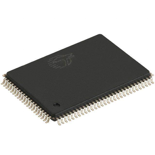
SL811HS Embedded USB Host/Slave Controller Embedded USB Host/Slave Controller Features Functional Description ■First USB Host/Slave controller for embedded systems in the The SL811HS is an Embedded USB Host/Slave Controller market with a standard microprocessor bus interface capable of communicating in either full speed or low speed. The SL811HS interfaces to devices such as microprocessors, micro- ■Supports both full speed (12 Mbps) and low speed (1.5 Mbps) controllers, DSPs, or directly to a variety of buses such as ISA, USB transfer in both master and slave modes PCMCIA, and others. The SL811HS USB Host Controller ■Conforms to USB Specification 1.1 for full- and low speed conforms to USB Specification 1.1. The SL811HS incorporates USB Serial Interface functionality ■Operates as a single USB host or slave under software control along with internal full or low speed transceivers. The SL811HS ■Automatic detection of either low- or full-speed devices supports and operates in USB full speed mode at 12 Mbps, or in low-speed mode at 1.5 Mbps. When in host mode, the SL811HS ■8-bit bidirectional data, port I/O (DMA supported in slave mode) is the master and controls the USB bus and the devices that are ■On-chip SIE and USB transceivers connected to it. In peripheral mode, otherwise known as a slave device, the SL811HS operates as a variety of full- or low-speed ■On-chip single root HUB support devices. ■256-byte internal SRAM buffer The SL811HS data port and microprocessor interface provide an 8-bit data path I/O or DMA bidirectional, with interrupt support to ■Ping-pong buffers for improved performance allow easy interface to standard microprocessors or ■Operates from 12 or 48 MHz crystal or oscillator (built-in DPLL) microcontrollers such as Motorola or Intel CPUs and many others. The SL811HS has 256 bytes of internal RAM, which is ■5 V-tolerant interface used for control registers and data buffers. ■Suspend/resume, wake up, and low-power modes are The available Pb-free package is a 48-pin (SL811HST-AXC) supported package. All packages operate at 3.3 VDC. The I/O interface logic is 5 V-tolerant. ■Auto-generation of SOF and CRC5/16 ■Auto-address increment mode, saves memory READ/WRITE cycles ■Development kit including source code drivers is available ■3.3-V power source, 0.35 micron CMOS technology ■Available in 48-pin TQFP package Logic Block Diagram Master/Slave Controller INTERRUPT INTR CONTROLLER 256 Byte RAM D USB SERIAL + INTERFACE BUFFERS nDRQ D- RootHUB & DMA ENGINE CONTROL XCVRS Interface REGISTERS nDACK nWR nRD PROCESSOR nCS CLOCK INTERFACE nRST GENERATOR D0-7 X1 X2 Errata: For information on silicon errata, see “Errata” on page33. Details include trigger conditions, devices affected, and proposed workaround. CypressSemiconductorCorporation • 198 Champion Court • SanJose, CA 95134-1709 • 408-943-2600 Document Number: 38-08008 Rev. *J Revised August 1, 2017
SL811HS Contents Functional Overview ........................................................3 Ordering Information ......................................................30 Data Port, Microprocessor Interface ............................3 Ordering Code Definitions .........................................30 DMA Controller (slave mode only) ..............................3 Package Diagram ............................................................31 Interrupt Controller ......................................................3 Acronyms ........................................................................32 Buffer Memory .............................................................4 Document Conventions .................................................32 PLL Clock Generator ...................................................5 Units of Measure .......................................................32 USB Transceiver .........................................................6 Errata ...............................................................................33 SL811HS Registers ...........................................................6 Part Numbers Affected ..............................................33 Physical Connections ....................................................21 SL811HS/SL811 Qualification Status ........................33 48-Pin TQFP Physical Connections ..........................21 SL811HS/SL811 Errata Summary ............................33 Electrical Specifications ................................................24 Document History Page .................................................37 Absolute Maximum Ratings .......................................24 Sales, Solutions, and Legal Information ......................39 Recommended Operating Conditions .......................24 Worldwide Sales and Design Support .......................39 External Clock Input Characteristics (X1) ..................24 Products ....................................................................39 DC Characteristics ....................................................25 PSoC® Solutions ......................................................39 USB Host Transceiver Characteristics ......................25 Cypress Developer Community .................................39 Bus Interface Timing Requirements ..........................26 Technical Support .....................................................39 Document Number: 38-08008 Rev. *J Page 2 of 39
SL811HS Functional Overview DMA Controller (slave mode only) In applications that require transfers of large amount of data, Data Port, Microprocessor Interface such as scanner interfaces, the SL811HS provides a DMA The SL811HS[1] microprocessor interface provides an 8-bit interface. This interface supports DMA READ or WRITE bidirectional data path along with appropriate control lines to transfers to the SL811HS internal RAM buffer, it is done through interface to external processors or controllers. Programmed I/O the microprocessor data bus via two control lines (nDRQ - Data or memory mapped I/O designs are supported through the 8-bit Request and nDACK - Data Acknowledge), along with the nWR interface, chip select, read and write input strobes, and a single line and controls the data flow into the SL811HS. The SL811HS address line, A0. has a count register that allows selection of programmable block Access to memory and control register space is a simple two sizes for DMA transfer. The control signals, both nDRQ and step process, requiring an address Write with A0 = ‘0’, followed nDACK, are designed for compatibility with standard DMA by a register/memory Read or Write cycle with address line interfaces. A0=‘1’. In addition, a DMA bidirectional interface in slave mode [2] is Interrupt Controller available with handshake signals such as nDRQ, nDACK, nWR, The SL811HS interrupt controller provides a single output signal nRD, nCS and INTRQ. (INTRQ) that is activated by a number of programmable events The SL811HS WRITE or READ operation terminates when that may occur as a result of USB activity. Control and status either nWR or nCS goes inactive. For devices interfacing to the registers are provided to allow the user to select single or SL811HS that deactivate the Chip Select nCS before the Write multiple events, which generate an interrupt (assert INTRQ) and nWR, the data hold timing must be measured from the nCS and let the user view interrupt status. The interrupts are cleared by is the same value as specified. Therefore, both Intel®- and writing to the Interrupt Status Register. Motorola-type CPUs work easily with the SL811HS without any external glue logic requirements. Notes 1. Errata: In a noisy environment, the SL811HS has the potential to occasionally miss a packet. Please refer to Errata on page 33 for details on errata and suggested work-around. 2. Errata: The DMA interface can be unreliable in slave mode. Please refer to Errata on page 33 for details on errata and suggested work-around. Document Number: 38-08008 Rev. *J Page 3 of 39
SL811HS Buffer Memory Auto Address Increment Mode [3] The SL811HS contains 256 bytes of internal memory used for The SL811HS supports the auto increment mode to reduce USB data buffers, control registers, and status registers. When READ and WRITE memory cycles. In this mode, the in master mode (host mode), the memory is defined where the microcontroller needs to set up the address only once. first 16 bytes are registers and the remaining 240 bytes are used Whenever any subsequent DATA is accessed, the internal for USB data buffers. When in slave mode (peripheral mode), the address counter advances to the next address location. first 64 bytes are used for the four endpoint control and status registers along with the various other registers. This leaves Auto Address Increment Example. To fill the data buffer that is 192bytes of endpoint buffer space for USB data transfers. configured for address 10h, follow these steps: 1.Write 10h to SL811HS with A0 LOW. This sets the memory Access to the registers and data memory is through the 8-bit address that is used for the next operation. external microprocessor data bus, in either indexed or direct addressing. Indexed mode uses the Auto Address Increment 2.Write the first data byte into address 10h by doing a write mode described in Auto Address Increment Mode [3], where operation with A0 HIGH. An example is a Get Descriptor; the direct addressing is used to READ/WRITE to an individual first byte that is sent to the device is 80h (bmRequestType) so address. you would write 80h to address 10h. USB transactions are automatically routed to the memory buffer 3.Now the internal RAM address pointer is set to 11h. So, by that is configured for that transfer. Control registers are provided doing another write with A0 HIGH, RAM address location 11h so that pointers and block sizes in buffer memory are determined is written with the data. Continuing with the Get Descriptor and allocated. example, a 06h is written to address 11h for the bRequest value. Figure 1. Memory Map 4.Repeat Step 3 until all the required bytes are written as 16 bytes 0x00 – 0x0F Control 0x00 – 0x39 necessary for a transfer. If auto-increment is not used, you and status registers 64 bytes Control/status registers write the address value each time before writing the data as and endpoint shown in Step 1. control/status registers The advantage of the auto address increment mode is that it 0x10 – 0xFF 0x40 – 0xFF reduces the number of required SL811HS memory 240 bytes USB data buffer USB data buffer READ/WRITE cycles to move data to/from the device. For 192 bytes example, transferring 64bytes of data to/from SL811HS, using auto increment mode, reduces the number of cycles to 1 address WRITE and 64 READ/WRITE data cycles, compared to 64 address writes and 64 data cycles for random access. Host Mode Memory Map Peripheral Mode Memory Map Note 3. Errata: The auto-increment feature can intermittently fail, causing the RAM location to be corrupted or the read buffer to provide incorrect data to the system processor. Please refer to Errata on page 33 for details on errata and suggested work-around. Document Number: 38-08008 Rev. *J Page 4 of 39
SL811HS PLL Clock Generator Figure 3. Optional 12 MHz Crystal Circuit Either a 12-MHz [4] or a 48-MHz external crystal is used with the SL811HS [5]. Two pins, X1 and X2, are provided to connect a low X1 X2 cost crystal circuit to the device as shown in Figure2 and Figure3. Use an external clock source if available in the Rf application instead of the crystal circuit by connecting the source directly to the X1 input pin. When a clock is used, the X2 pin is 1M not connected. Rs 100 When the CM pin is tied to a logic 0, the internal PLL is bypassed so the clock source must meet the timing requirements specified X1 by the USB specification. Figure 2. Full Speed 48 MHz Crystal Circuit 12 MHz , series, 20-pF load X1 X2 Cin Cout 22 pF 22 pF Rf 1M Typical Crystal Requirements Rs The following are examples of ‘typical requirements.’ Note that X1 100 these specifications are generally found as standard crystal values and are less expensive than custom values. If crystals are 48 MHz, series, 20-pF load used in series circuits, load capacitance is not applicable. Load capacitance of parallel circuits is a requirement. The 48-MHz third overtone crystals require the Cin/Lin filter to guarantee Cbk 48-MHz operation. 0.01 F 12 MHz Crystals: Cout Frequency Tolerance: ±100 ppm or better Lin Cin 22 pF 2.2 H Operating Temperature Range: 0 C to 70 C 22 pF Frequency: 12 MHz Frequency Drift over Temperature: ± 50 ppm ESR (Series Resistance): 60 Load Capacitance: 10 pF min Shunt Capacitance: 7 pF max Drive Level: 0.1–0.5 mW Operating Mode: fundamental 48 MHz Crystals: Frequency Tolerance: ±100 ppm or better Operating Temperature Range: 0 C to 70 C Frequency: 48 MHz Frequency Drift over Temperature: ± 50 ppm ESR (Series Resistance): 40 Load Capacitance: 10 pF min Shunt Capacitance: 7 pF max Drive Level: 0.1–0.5 mW Operating Mode: third overtone Notes 4. Errata: The internal PLL is very sensitive. The PLL causes any high-frequency noise on the VDD pins to result in clock jitter. Refer to Errata on page 33 for details on errata and suggested work-around. 5. CM (Clock Multiply) pin of the SL811HS must be tied to GND when 48 MHz crystal circuit or 48 MHz clock source is used. Document Number: 38-08008 Rev. *J Page 5 of 39
SL811HS USB Transceiver Table 1. SL811HS Master (Host) Mode Registers The SL811HS has a built-in transceiver that meets USB Specification 1.1. The transceiver is capable of transmitting and Register Name SL811HS receiving serial data at USB full speed [6] (12 Mbits) and low SL811HS (hex) Address speed [7] (1.5 Mbits). The driver portion of the transceiver is USB-A Host Control Register 00h differential while the receiver section is comprised of a differential USB-A Host Base Address 01h receiver and two single-ended receivers. Internally, the transceiver interfaces to the Serial Interface Engine (SIE) logic. USB-A Host Base Length 02h Externally, the transceiver connects to the physical layer of the USB-A Host PID, Device Endpoint 03h USB. (Write)/USB Status (Read) USB-A Host Device Address 04h SL811HS Registers (Write)/Transfer Count (Read) Operation and control of the SL811HS is managed through Control Register 1 05h internal registers. When operating in Master/Host mode, the first Interrupt Enable Register 06h 16 address locations are defined as register space. In Slave/Peripheral mode, the first 64 bytes are defined as register Reserved Register Reserved space. The register definitions vary greatly between each mode USB-B Host Control Register 08h of operation and are defined separately in this document (section USB-B Host Base Address 09h Table1 describes Host register definitions, while Table 19 on page 15 describes Slave register definitions). Access to the USB-B Host Base Length 0Ah registers are through the microprocessor interface similar to USB-B Host PID, Device Endpoint 0Bh normal RAM accesses (see “Bus Interface Timing (Write)/USB Status (Read) Requirements” on page26) and provide control and status information for USB transactions. USB-B Host Device Address 0Ch (Write)/Transfer Count (Read) Any write to control register 0FH enables the SL811HS full features bit. This is an internal bit of the SL811HS that enables Status Register 0Dh additional features. SOF Counter LOW (Write)/HW Revision 0Eh Table1 shows the memory map and register mapping of the Register (Read) SL811HS in master/host mode. SOF Counter HIGH and Control Register 2 0Fh Memory Buffer 10H-FFh The registers in the SL811HS are divided into two major groups. The first group is referred to as USB Control registers. These registers enable and provide status for control of USB transactions and data flow. The second group of registers provides control and status for all other operations. Register Values on Power-up and Reset The following registers initialize to zero on power-up and reset: ■USB-A/USB-B Host Control Register [00H, 08H] bit 0 only ■Control Register 1 [05H] ■USB Address Register [07H] ■Current Data Set/Hardware Revision/SOF Counter LOW Register [0EH] All other register’s power-up and reset in an unknown state and firmware for initialization. Notes 6. Errata: The SYNC to SOF bit (bit 5) of the USB Host Control Registers [00H, 08H], is only designed for full-speed support. In full-speed mode, this bit should only be used when the software cannot fit a packet within the remaining 1 ms frame. Please refer to Errata on page 33 for details on errata and suggested work-around. 7. Errata: Some hubs that send SE0s upstream during the EOF1 time frame may cause the SL811HS to stop sending SOFs. This problem occurs when operating with low-speed devices attached downstream of such a hub. Please refer to Errata on page 33 for details on errata and suggested work-around. Document Number: 38-08008 Rev. *J Page 6 of 39
SL811HS USB Control Registers Table 2. SL811HS Host Control Registers Communication and data flow on the USB bus uses the SL811HS’ USB A-B Control registers. The SL811HS communi- SL811HS Register Name SL811H cates with any USB Device function and any specific endpoint (hex) Address via the USB-A or USB-B register sets. USB-A Host Control Register 00h The USB A-B Host Control registers are used in an overlapped USB-A Host Base Address 01h configuration to manage traffic on the USB bus. The USB Host Control register also provides a means to interrupt an external USB-A Host Base Length 02h CPU or microcontroller when one of the USB protocol transac- USB-A Host PID, Device Endpoint 03h tions is completed. Table1 and Table2 show the two sets of USB (Write)/USB Status (Read) Host Control registers, the ’A’ set and ’B’ set. The two register USB-A Host Device Address 04h sets allow for overlapping operation. When one set of param- (Write)/Transfer Count (Read) eters is being set up, the other is transferring. On completion of a transfer to an endpoint, the next operation is controlled by the USB-B Host Control Register 08h other register set. USB-B Host Base Address 09h Note The USB-B register set is used only when SL811HS mode USB-B Host Base Length 0Ah is enabled by initializing register 0FH. USB-B Host PID, Device Endpoint 0Bh The SL811HS USB Host Control has two groups of five registers (Write)/USB Status (Read) each which map in the SL811HS memory space. These registers are defined in the following tables. USB-B Host Device Address 0Ch (Write)/Transfer Count (Read) Document Number: 38-08008 Rev. *J Page 7 of 39
SL811HS USB-A/USB-B Host Control Registers [Address = 00h, 08h] . Table 3. USB-A/USB-B Host Control Register Definition [Address 00h, 08h] Bit 7 Bit 6 Bit 5 Bit 4 Bit 3 Bit 2 Bit 1 Bit 0 Preamble Data Toggle Bit SyncSOF ISO Reserved Direction Enable Arm Bit Position Bit Name Function 7 Preamble If bit = ‘1’ a preamble token is transmitted before transfer of low speed packet. If bit =‘0’, preamble generation is disabled. ■The SL811HS automatically generates preamble packets when bit 7 is set. This bit is only used to send packets to a low speed device through a hub. To communicate to a full speed device, this bit is set to ‘0’. For example, when SL811HS communicates to a low speed device via the HUB: —SetSL811HS SIE to operate at full speed, i.e., bit 5 of register 05h (Control Register1) = ‘0’. —Set bit 6 of register 0Fh (Control Register 2) = ‘0’. Set correct polarity of DATA+ and DATA– state for full speed. —Set bit 7, Preamble bit, = ‘1’ in the Host Control register. ■When SL811HS communicates directly to a low speed device: —Set bit 5 of register 05h (Control Register 1) = ‘1’. — Set bit 6 of register 0Fh (Control Register 2) = ‘1’, DATA+ and DATA– polarity for low speed. —The state of bit 7 is ignored in this mode. 6 Data Toggle Bit ’0’ if DATA0, ‘1’ if DATA1 (only used for OUT tokens in host mode). 5 SyncSOF ’1’ = Synchronize with the SOF transfer when operating in FS only. The SL811HS uses bit 5 to enable transfer of a data packet after a SOF packet is transmitted. When bit 5 = ‘1’, the next enabled packet is sent after next SOF. If bit 5 = ‘0’ the next packet is sent immediately if the SIE is free. If operating in low speed, do not set this bit. 4 ISO When set to ‘1’, this bit allows Isochronous mode for this packet. 3 Reserved Bit 3 is reserved for future use. 2 Direction When equal to ‘1’ transmit (OUT). When equal to ‘0’ receive (IN). 1 Enable If Enable = ‘1’, this bit allows transfers to occur. If Enable = ‘0’, USB transactions are ignored. The Enable bit is used in conjunction with the Arm bit (bit 0 of this register) for USB transfers. 0 Arm Allows enabled transfers when Arm = ‘1’. Cleared to ‘0’ when transfer is complete (when Done Interrupt is asserted). Once the other SL811HS Control registers are configured (registers 01h-04h or 09h-0Ch) the Host Control register is programmed to initiate the USB transfer. This register initiates the transfer when the Enable and Arm bit are set as described above. USB-A/USB-B Host Base Address [Address = 01h, 09h] . Table 4. USB-A/USB-B Host Base Address Definition [Address 01h, 09h] Bit 7 Bit 6 Bit 5 Bit 4 Bit 3 Bit 2 Bit 1 Bit 0 HBADD7 HBADD6 HBADD5 HBADD4 HBADD3 HBADD2 HBADD1 HBADD0 The USB-A/B Base Address is a pointer to the SL811HS memory buffer location for USB reads and writes. When transferring data OUT (Host to Device), the USB-A and USB-B Host Base Address registers can be set up before setting ARM on the USB-A or USB-B Host Control register. When using a double buffer scheme, the Host Base Address could be set up with the first buffer used for DATA0 data and the other for DATA1 data. Document Number: 38-08008 Rev. *J Page 8 of 39
SL811HS USB-A/USB-B Host Base Length [Address = 02h, 0Ah]. Table 5. USB-A / USB-B Host Base Length Definition [Address 02h, 0Ah] Bit 7 Bit 6 Bit 5 Bit 4 Bit 3 Bit 2 Bit 1 Bit 0 HBL7 HBL6 HBL5 HBL4 HBL3 HBL2 HBL1 HBL0 The USB A/B Host Base Length register contains the maximum packet size transferred between the SL811HS and a slave USB peripheral. Essentially, this designates the largest packet size that is transferred by the SL811HS. Base Length designates the size of data packet sent or received. For example, in full speed BULK mode, the maximum packet length is 64 bytes. In ISO mode, the maximum packet length is 1023 bytes since the SL811HS only has an 8-bit length; the maximum packet size for the ISO mode using the SL811HS is 255 – 16 bytes (register space). When the Host Base length register is set to zero, a Zero-Length packet is transmitted. USB-A/USB-B USB Packet Status (Read) and Host PID, Device Endpoint (Write) [Address = 03h, 0Bh]. This register has two modes dependent on whether it is read or written. When read, this register provides packet status and contains information relative to the last packet that has been received or transmitted. This register is not valid for reading until after the Done interrupt occurs, which causes the register to update. Table 6. USB-A/USB-B USB Packet Status Register Definition when READ [Address 03h, 0Bh] Bit 7 Bit 6 Bit 5 Bit 4 Bit 3 Bit 2 Bit 1 Bit 0 STALL NAK Overflow Setup Sequence Time-out Error ACK Bit Position Bit Name Function 7 STALL Slave device returned a STALL. 6 NAK Slave device returned a NAK. 5 Overflow Overflow condition - maximum length exceeded during receives. For underflow, see USB-A/USB-B Host Transfer Count Register (Read), USB Address (Write) [Address = 04h, 0Ch]. 4 Setup This bit is not applicable for Host operation since a SETUP packet is generated by the host. 3 Sequence Sequence bit. ‘0’ if DATA0, ‘1’ if DATA1. 2 Time-out Timeout occurred. A timeout is defined as 18-bit times without a device response (in full speed). 1 Error Error detected in transmission. This includes CRC5, CRC16, and PID errors. 0 ACK Transmission Acknowledge. When written, this register provides the PID and Endpoint information to the USB SIE engine used in the next transaction. All 16 Endpoints can be addressed by the SL811HS. Table 7. USB-A / USB-B Host PID and Device Endpoint Register when WRITTEN [Address 03h, 0Bh] Bit 7 Bit 6 Bit 5 Bit 4 Bit 3 Bit 2 Bit 1 Bit 0 PID3 PID2 PID1 PID0 EP3 EP2 EP1 EP0 PID[3:0]: 4-bit PID Field (See following table), EP[3:0]: 4-bit Endpoint Value in Binary. PID TYPE D7–D4 SETUP 1101 (D Hex) IN 1001 (9 Hex) OUT 0001 (1 Hex) SOF 0101 (5 Hex) PREAMBLE 1100 (C Hex) NAK 1010 (A Hex) STALL 1110 (E Hex) DATA0 0011 (3 Hex) DATA1 1011 (B Hex) Document Number: 38-08008 Rev. *J Page 9 of 39
SL811HS USB-A/USB-B Host Transfer Count Register (Read), USB Address (Write) [Address = 04h, 0Ch]. This register has two different functions depending on whether it is read or written. When read, this register contains the number of bytes remaining (from Host Base Length value) after a packet is transferred. For example, if the Base Length register is set to 0x040 and an IN Token was sent to the peripheral device. If, after the transfer is complete, the value of the Host Transfer Count is 0x10, the number of bytes actually transferred is 0x30. This is considered as an underflow indication. Table 8. USB-A / USB-B Host Transfer Count Register when READ [Address 04h, 0Ch] Bit 7 Bit 6 Bit 5 Bit 4 Bit 3 Bit 2 Bit 1 Bit 0 HTC7 HTC6 HTC5 HTC4 HTC3 HTC2 HTC1 HTC0 When written, this register contains the USB Device Address with which the Host communicates. Table 9. USB-A / USB-B USB Address when WRITTEN [Address 04h, 0Ch] Bit 7 Bit 6 Bit 5 Bit 4 Bit3 Bit 2 Bit 1 Bit 0 0 DA6 DA5 DA4 DA3 DA2 DA1 DA0 DA6-DA0 Device address, up to 127 devices can be addressed. DA7 Reserved bit must be set to zero. SL811HS Control Registers The next set of registers are the Control registers and control more of the operation of the chip instead of USB packet type of transfers. Table10 is a summary of the control registers. Table 10. Control Registers Summary Register Name SL811H SL811HS (hex) Address Control Register 1 05h Interrupt Enable Register 06h Reserved Register 07h Status Register 0Dh SOF Counter LOW (Write)/HW Revision Register (Read) 0Eh SOF Counter HIGH and Control Register 2 0Fh Memory Buffer 10h-FFh Document Number: 38-08008 Rev. *J Page 10 of 39
SL811HS Control Register 1 [Address = 05h]. The Control Register 1 enables/disables USB transfer operation with control bits defined as follows. Table 11. Control Register 1 [Address 05h] Bit 7 Bit 6 Bit 5 Bit 4 Bit 3 Bit 2 Bit 1 Bit 0 Reserved Suspend USB Speed J-K state force USB Engine Reserved Reserved SOF ena/dis Reset Bit Position Bit Name Function 7 Reserved ‘0’ 6 Suspend ’1’ = enable, ‘0’ = disable. 5 USB Speed ’0’ setup for full speed, ‘1’ setup low speed. 4 J-K state force See Table12. 3 USB Engine Reset USB Engine reset = ‘1’. Normal set ‘0’. When a device is detected, the first thing that to do is to send it a USB Reset to force it into its default address of zero. The USB 2.0 specification states that for a root hub a device must be reset for a minimum of 50 mS. 2 Reserved Some existing firmware examples set bit 2, but it is not necessary. 1 Reserved ‘0’ 0 SOF ena/dis ’1’ = enable auto Hardware SOF generation; ‘0’ = disable. In the SL811HS, bit 0 is used to enable hardware SOF auto-generation. The generation of SOFs continues when set to ‘0’, but SOF tokens are not output to USB. At power-up this register is cleared to all zeros. There are two cases when communicating with a low speed device. When a low speed device is connected directly to the Low-power Modes [Bit 6 Control Register, Address 05h] SL811HS, bit 5 of Register 05h is set to ‘1’ and bit 6 of register When bit 6 (Suspend) is set to ‘1’, the power of the transmit 0Fh, Polarity Swap, is set to ‘1’ in order to change the polarity of transceiver is turned off, the internal RAM is in suspend mode, D+ and D–. When a low speed device is connected via a HUB to and the internal clocks are disabled. SL811HS, bit 5 of Register 05h is set to ‘0’ and bit 6 of register 0Fh is set to ’0’ in order to keep the polarity of D+ and D– for full Note Any activity on the USB bus (that is, K-State, etc.) resumes speed. In addition, make sure that bit7 of USB-A/USB-B Host normal operation. To resume normal operation from the CPU Control registers [00h, 08h] is set to ‘1’ for preamble generation. side, a Data Write cycle (i.e., A0 set HIGH for a Data Write cycle) is done. This is a special case and not a normal direct write J-K Programming States [Bits 4 and 3 of Control Register 1, where the address is first written and then the data. To resume Address 05h] normal operation from the CPU side, you must do a Data Write The J-K force state control and USB Engine Reset bits are used cycle only. to generate a USB reset condition. Forcing K-state is used for Low Speed/Full Speed Modes [Bit 5 Control Register 1, Peripheral device remote wake up, resume, and other modes. Address 05h] These two bits are set to zero on power-up. The SL811HS is designed to communicate with either full- or low speed devices. At power-up bit 5 is LOW, i.e., for full speed. Table 12. Bus Force States USB Engine J-K Force Function Reset State 0 0 Normal operating mode 0 1 Force USB Reset, D+ and D– are set LOW (SE0) 1 0 Force J-State, D+ set HIGH, D– set LOW[8] 1 1 Force K-State, D– set HIGH, D+ set LOW[9] Notes 8. Force K-State for low speed. 9. Force J-State for low speed. Document Number: 38-08008 Rev. *J Page 11 of 39
SL811HS USB Reset Sequence Interrupt Enable Register [Address = 06h]. The SL811HS provides an Interrupt Request Output, which is activated for a After a device is detected, write 08h to the Control register (05h) number of conditions. The Interrupt Enable register allows the to initiate the USB reset, then wait for the USB reset time (root user to select conditions that result in an interrupt that is issued hub should be 50 ms) and additionally some types of devices to an external CPU through the INTRQ pin. A separate Interrupt such as a Forced J-state. Lastly, set the Control register (05h) Status register reflects the reason for the interrupt. Enabling or back to 0h. After the reset is complete, the auto-SOF generation disabling these interrupts does not have an effect on whether or is enabled. not the corresponding bit in the Interrupt Status register is set or SOF Packet Generation cleared; it only determines if the interrupt is routed to the INTRQ The SL811HS automatically computes the frame number and pin. The Interrupt Status register is normally used in conjunction CRC5 by hardware. No CRC or SOF generation is required by with the Interrupt Enable register and can be polled in order to external firmware for the SL811HS, although it can be done by determine the conditions that initiated the interrupt (See the sending an SOF PID in the Host PID, Device Endpoint register. description for the Interrupt Status Register). When a bit is set to ’1’ the corresponding interrupt is enabled. So when the enabled To enable SOF generation, assuming host mode is configured: interrupt occurs, the INTRQ pin is asserted. The INTRQ pin is a 1.Set up the SOF interval in registers 0x0F and 0x0E. level interrupt, meaning it is not deasserted until all enabled inter- 2.Enable the SOF hardware generation in this register by rupts are cleared. setting bit 0 = ‘1’. 3.Set the Arm bit in the USB-A Host Control register. Table 13. Interrupt Enable Register [Address 06h] Bit 7 Bit 6 Bit 5 Bit 4 Bit 3 Bit 2 Bit 1 Bit 0 Reserved Device Inserted/ SOF Timer Reserved Reserved USB-B USB-A Detect/Resum Removed DONE DONE e Bit Position Bit Name Function 7 Reserved ‘0’ 6 Device Detect/Resume Enable Device Detect/Resume Interrupt. When bit 6 of register 05h (Control Register 1) is equal to ’1’, bit 6 of this register enables the Resume Detect Interrupt. Otherwise, this bit is used to enable Device Detection status as defined in the Interrupt Status register bit definitions. 5 Inserted/Removed Enable Slave Insert/Remove Detection is used to enable/disable the device inserted/removed interrupt. 4 SOF Timer 1 = Enable Interrupt for SOF Timer. This is typically at 1 mS intervals, although the timing is determined by the SOF Counter high/low registers. To use this bit function, bit 0 of register 05h must be enabled and the SOF counter registers 0E hand 0Fh must be initialized. 3 Reserved ‘0’ 2 Reserved ‘0’ 1 USB-B DONE USB-B Done Interrupt (see USB-A Done interrupt). 0 USB-A DONE USB-A Done Interrupt. The Done interrupt is triggered by one of the events that are logged in the USB Packet Status register. The Done interrupt causes the Packet Status register to update. USB Address Register, Reserved, Address [Address = 07h]. This register is reserved for the device USB Address in Slave operation. It should not be written by the user in host mode. Registers 08h-0Ch Host-B registers. Registers 08h-0Ch have the same definition as registers 00h-04h except they apply to Host-B instead of Host-A. Document Number: 38-08008 Rev. *J Page 12 of 39
SL811HS Interrupt Status Register, Address [Address = 0Dh]. The Interrupt Status register is a READ/WRITE register providing interrupt status. Interrupts are cleared by writing to this register. To clear a specific interrupt, the register is written with corresponding bit set to ‘1’. Table 14. Interrupt Status Register [Address 0Dh] Bit 7 Bit 6 Bit 5 Bit 4 Bit 3 Bit 2 Bit 1 Bit 0 D+ Device Insert/Remove SOF timer Reserved Reserved USB-B USB-A Detect/Resum e Bit Position Bit Name Function 7 D+ Value of the Data+ pin. Bit 7 provides continuous USB Data+ line status. Once it is determined that a device is inserted (as described below) with bits 5 and 6, bit 7 is used to detect if the inserted device is low speed (0) or full speed (1). 6 Device Detect/Resume Device Detect/Resume Interrupt. Bit 6 is shared between Device Detection status and Resume Detection interrupt. When bit-6 of register 05h is set to one, this bit is the Resume detection Interrupt bit. Otherwise, this bit is used to indicate the presence of a device, ‘1’ = device ‘Not present’ and ‘0’ = device ‘Present.’ In this mode, check this bit along with bit 5 to determine whether a device has been inserted or removed. 5 Insert/Remove Device Insert/Remove Detection. Bit 5 is provided to support USB cable insertion/removal for the SL811HS in host mode. This bit is set when a transition from SE0 to IDLE (device inserted) or from IDLE to SE0 (device removed) occurs on the bus. 4 SOF timer ‘1’ = Interrupt on SOF Timer. 3 Reserved ‘0’ 2 Reserved ‘0’ 1 USB-B USB-B Done Interrupt. (See description in Interrupt Enable Register [address 06h].) 0 USB-A USB-A Done Interrupt. (See description in Interrupt Enable Register [address 06h].) Current Data Set Register/Hardware Revision/SOF Counter LOW [Address = 0Eh]. This register has two modes. Read from this register indicates the current SL811HS silicon revision. Table 15. Hardware Revision when Read [Address 0Eh] Bit 7 Bit 6 Bit 5 Bit 4 Bit 3 Bit 2 Bit 1 Bit 0 Hardware Revision Reserved Bit Position Bit Name Function 7-4 Hardware Revision SL811HS rev1.2 Read = 1H; SL811HS rev1.5 Read = 2. 3-2 Reserved Read is zero. 1-0 Reserved Reserved for slave. Writing to this register sets up auto generation of SOF to all connected peripherals. This counter is based on the 12 MHz clock and is not dependent on the crystal frequency. To set up a 1 ms timer interval, the software must set up both SOF counter registers to the proper values. Table 16. SOF Counter LOW Address when Written [Address 0Eh] Bit 7 Bit 6 Bit 5 Bit 4 Bit 3 Bit 2 Bit 1 Bit 0 SOF7 SOF6 SOF5 SOF4 SOF3 SOF2 SOF1 SOF0 Example: To set up SOF for 1 ms interval, SOF counter register 0Eh should be set to E0h. Document Number: 38-08008 Rev. *J Page 13 of 39
SL811HS SOF Counter High/Control Register 2 [Address = 0Fh]. When read, this register returns the value of the SOF counter divided by 64. The software must use this register to determine the available bandwidth in the current frame before initiating any USB transfer. In this way, the user is able to avoid babble conditions on the USB. For example, to determine the available bandwidth left in a frame do the following. Maximum number of clock ticks in 1 ms time frame is 12000 (1 count per 12 MHz clock period, or approximately 84 ns.) The value read back in Register 0FH is the (count × 64) × 84 ns = time remaining in current frame. USB bit time = one 12 MHz period. Value of register 0FH Available bit times left are between BBH 12000 bits to 11968 (187 × 64) bits BAH 11968 bits to 11904 (186 × 64) bits Note: Any write to the 0Fh register clears the internal frame counter. Write register 0Fh at least once after power-up. The internal frame counter is incremented after every SOF timer tick. The internal frame counter is an 11-bit counter, which is used to track the frame number. The frame number is incremented after each timer tick. Its contents are transmitted to the slave every millisecond in a SOF packet. Table 17. SOF High Counter when Read [Address 0Fh] Bit 7 Bit 6 Bit 5 Bit 4 Bit 3 Bit 2 Bit 1 Bit 0 C13 C12 C11 C10 C9 C8 C7 C6 When writing to this register the bits definition are defined as follows. Table 18. Control Register 2 when Written [Address 0Fh] Bit 7 Bit 6 Bit 5 Bit 4 Bit 3 Bit 2 Bit 1 Bit 0 SL811HS SL811HS SOF High Counter Register Master/Slave D+/D– Data selection Polarity Swap Bit Position Bit Name Function 7 SL811HS Master/Slave selection Master = 1, Slave = 0. 6 SL811HS D+/D– Data Polarity Swap ’1’ = change polarity (low speed) ’0’ = no change of polarity (full speed). 5-0 SOF High Counter Register Write a value or read it back to SOF High Counter Register. Note Any write to Control register 0Fh enables the SL811HS full hardware SOF generation. To load both HIGH and LOW features bit. This is an internal bit of the SL811HS that enables registers with the proper values, the user must follow this additional features. sequence: The USB-B register set is used when SL811HS full feature bit is 1.Write E0h to register 0Eh. This sets the lower byte of the SOF enabled. counter Example. To set up host to generate 1 ms SOF time: 2.Write AEh to register 0Fh, AEh configures the part for full speed (no change of polarity) Host with bits 5–0 = 2Eh for The register 0Fh contains the upper 6 bits of the SOF timer. upper portion of SOF counter. Register 0Eh contains the lower 8 bits of the SOF timer. The timer is based on an internal 12-MHz clock and uses a counter, 3.Enable bit 0 in register 05h. This enables hardware generation of SOF. which counts down to zero from an initial value. To set the timer for 1 ms time, the register 0Eh is loaded with value E0h and 4.Set the ARM bit at address 00h. This starts the SOF register 0Fh (bits 0–5) is loaded with 2Eh. To start the timer, bit generation. 0 of register 05h (Control Register 1) is set to ’1’, which enables Document Number: 38-08008 Rev. *J Page 14 of 39
SL811HS Table 19. SL811HS Slave Mode Registers Endpoint specific register addresses Register Name EP 0 – A EP 0 - B EP 1 – A EP 1 - B EP 2 - A EP 2 - B EP 3 - A EP 3 - B EP Control Register 00h 08h 10h 18h 20h 28h 30h 0x38 EP Base Address Register 01h 09h 11h 19h 21h 29h 31h 0x39 EP Base Length Register 02h 0Ah 12h 1Ah 22h 2Ah 0x32 0x3A EP Packet Status Register 03h 0Bh 13h 1Bh 23h 2Bh 0x33 0x3B EP Transfer Count Register 04h 0Ch 14h 1Ch 24h 2Ch 0x34 0x3C Register Name Miscellaneous register addresses Control Register 1 05h Interrupt Status Register 0Dh Interrupt Enable Register 06h Current Data Set Register 0Eh USB Address Register 07h Control Register 2 0Fh SOF Low Register (read only) 15h Reserved 1Dh1Fh SOF High Register (read only) 16h Reserved 25h-27h Reserved 17h Reserved 2Dh-2Fh DMA Total Count Low Register 35h DMA Total Count High Register 36h Reserved 37h Memory Buffer 40h–FFh When in slave mode, the registers in the SL811HS are divided Endpoints 0–3 Register Addresses into two major groups. The first group contains Endpoint regis- Each endpoint set has a group of five registers that are mapped ters that manage USB control transactions and data flow. The within the SL811HS memory. The register sets have address second group contains the USB Registers that provide the con- assignments Endpoint 0–3 Register Addresses as shown in the trol and status information for all other operations. following table. Endpoint Registers Table 20. Endpoint 0–3 Register Addresses Communication and data flow on USB is implemented using Endpoint Register Set Address (in Hex) endpoints. These uniquely identifiable entities are the terminals of communication flow between a USB host and USB devices. Endpoint 0 – a 00 - 04 Each USB device is composed of a collection of independently Endpoint 0 – b 08 - 0C operating endpoints. Each endpoint has a unique identifier, Endpoint 1 – a 10 - 14 which is the Endpoint Number. For more information, see USB Specification 1.1 section 5.3.1. Endpoint 1 – b 18 - 1C The SL811HS supports four endpoints numbered 0–3. Endpoint Endpoint 2 – a 20 - 24 0 is the default pipe and is used to initialize and generically Endpoint 2 – b 28 - 2C manipulate the device to configure the logical device as the Endpoint 3 – a 30 - 34 Default Control Pipe. It also provides access to the device's Endpoint 3 – b 38 - 3C configuration information, allows USB status and control access, and supports control transfers. For each endpoint set (starting at address Index = 0), the Endpoints 1–3 support Bulk, Isochronous, and Interrupt registers are mapped as shown in the following table. transfers. Endpoint 3 is supported by DMA. Each endpoint has two sets of registers—the ‘A’ set and the ‘B’ set. This allows Table 21. Endpoint Register Indices overlapped operation where one set of parameters is set up and the other is transferring. Upon completion of a transfer to an Endpoint Register Sets endpoint, the ‘next data set’ bit indicates whether set ‘A’ or set ‘B’ (for Endpoint n starting at register position Index=0) is used next. The ‘armed’ bit of the next data set indicates Index Endpoint n Control whether the SL811HS is ready for the next transfer without inter- Index + 1 Endpoint n Base Address ruption. Index + 2 Endpoint n Base Length Index + 3 Endpoint n Packet Status Index + 4 Endpoint n Transfer Count Document Number: 38-08008 Rev. *J Page 15 of 39
SL811HS Endpoint Control Registers Endpoint n Control Register [Address a = (EP# * 10h), b = (EP# * 10h)+8]. Each endpoint set has a Control register defined as follows: Table 22. Endpoint Control Register [Address EP0a/b:00h/08h, EP1a/b:10h/18h, EP2a/b:20h/28h, EP3a/b:30h/38h] 7 6 5 4 3 2 1 0 Reserved Sequence Send STALL ISO Next Data Set Direction Enable Arm Bit Position Bit Name Function 7 Reserved 6 Sequence Sequence bit. ‘0’ if DATA0, ‘1’ if DATA1. 5 Send STALL When set to ‘1’, sends Stall in response to next request on this endpoint. 4 ISO When set to ‘1’, allows Isochronous mode for this endpoint. 3 Next Data Set '0' if next data set is ‘A’, ‘1’ if next data set is 'B'. 2 Direction When Direction = ‘1’, transmit to Host (IN). When Direction = ‘0’, receive from Host (OUT). 1 Enable When Enable = ‘1’, allows transfers for this endpoint. When set to ‘0’, USB transactions are ignored. If Enable = ‘1’ and Arm = ‘0’, the endpoint returns NAKs to USB transmissions. 0 Arm Allows enabled transfers when set = ‘1’. Clears to ‘0’ when transfer is complete. Endpoint Base Address [Address a = (EP# * 10h)+1, b = (EP# * 10h)+9]]. Pointer to memory buffer location for USB reads and writes. Table 23. Endpoint Base Address Reg [Address; EP0a/b:01h/09h, EP1a/b:11h/19h, EP2a/b:21h/29h, EP3a/b:31h/39h] 7 6 5 4 3 2 1 0 EPxADD7 EPxADD6 EPxADD5 EPxADD4 EPxADD3 EPxADD2 EPxADD1 EPxADD0 Endpoint Base Length [Address a = (EP# * 10h)+2, b = (EP# * 10h)+A]. The Endpoint Base Length is the maximum packet size for IN/OUT transfers with the host. Essentially, this designates the largest packet size that is received by the SL811HS with an OUT transfer, or it designates the size of the data packet sent to the host for IN transfers. Table 24. Endpoint Base Length Reg [Address EP0a/b:02h/0Ah, EP1a/b:12h/1Ah, EP2a/b:22h/2Ah, EP3a/b:32h/3Ah] 7 6 5 4 3 2 1 0 EPxLEN7 EPxLEN6 EPxLEN5 EPxLEN4 EPxLEN3 EPxLEN2 EPxLEN1 EPxLEN0 Document Number: 38-08008 Rev. *J Page 16 of 39
SL811HS Endpoint Packet Status [Address a = (EP# * 10h)+3, b = (EP# * 10h)+Bh]. The packet status contains information relative to the packet that is received or transmitted. The register is defined as follows: Table 25. Endpoint Packet Status Reg [Address EP0a/b:03h/0Bh, EP1a/b:13h/1Bh, EP2a/b:23h/2Bh, EP3a/b:33h/3Bh] 7 6 5 4 3 2 1 0 Reserved Reserved Overflow Setup Sequence Time-out Error ACK Bit Position Bit Name Function 7 Reserved Not applicable. 6 Reserved Not applicable. 5 Overflow Overflow condition - maximum length exceeded during receives. This is considered a serious error. The maximum number of bytes that can be received by an endpoint is determined by the Endpoint Base Length register for each endpoint. The Overflow bit is only relevant during OUT Tokens from the host. 4 Setup '1' indicates Setup Packet. If this bit is set, the last packet received was a setup packet. 3 Sequence This bit indicates if the last packet was a DATA0 (0) or DATA1 (1). 2 Time-out This bit is not used in slave mode. 1 Error Error detected in transmission, this includes CRC5/16 and PID errors. 0 ACK Transmission Acknowledge. Endpoint Transfer Count [Address a = (EP# * 10h)+4, b = register was set for 64 (40h) bytes and an OUT token was sent (EP# * 10h)+Ch]. As a peripheral device, the Endpoint Transfer to the endpoint that only had 16 (10h) bytes, the Endpoint Count register is only important with OUT tokens (host sending Transfer Count register has a value of 48 (30h). If more bytes the slave data). When a host sends the peripheral data, the were sent in an OUT token then the Endpoint Base Length Transfer Count register contains the difference between the register was programmed for, the overflow flag is set in the Endpoint Base Length and the actual number of bytes received Endpoint Packet Status register and is considered a serious in the last packet. In other words, if the Endpoint Base Length error. Table 26. Endpoint Transfer Count Reg [Address EP0a/b:04h/0Ch, EP1a/b:14h/1Ch, EP2a/b:24h/2Ch, EP3a/b:34h/3Ch] 7 6 5 4 3 2 1 0 EPxCNT7 EPxCNT6 EPxCNT5 EPxCNT4 EPxCNT3 EPxCNT2 EPxCNT1 EPxCNT0 USB Control Registers The USB Control registers manage communication and data flow on the USB. Each USB device is composed of a collection of independently operating endpoints. Each endpoint has a unique identifier, which is the Endpoint Number. For more details about USB endpoints, refer to the USB Specification 1.1, Section 5.3.1. The Control and Status registers are mapped as follows: Table 27. USB Control Registers Register Name Address (in Hex) Control Register 1 05h Interrupt Enable Register 06h USB Address Register 07h Interrupt Status Register 0Dh Current Data Set Register 0Eh Control Register 2 0Fh SOF Low Byte Register 15h SOF High Byte Register 16h DMA Total Count Low Byte Register 35h DMA Total Count High Byte Register 36h Document Number: 38-08008 Rev. *J Page 17 of 39
SL811HS Control Register 1, Address [05h]. The Control register enables or disables USB transfers and DMA operations with control bits. Table 28. Control Register 1 [Address 05h] 7 6 5 4 3 2 1 0 Reserved STBYD SPSEL J-K1 J-K0 DMA Dir DMA Enable USB Enable Bit Position Bit Name Function 7 Reserved Reserved bit - must be set to '0'. 6 STBYD XCVR Power Control. ‘1’ sets XCVR to low power. For normal operation set this bit to ‘0’. Suspend mode is entered if bit 6 = ‘1’ and bit ‘0’ (USB Enable) = ‘0’. 5 SPSEL Speed Select. ‘0’ selects full speed. ‘1’ selects low speed (also see Table33 on page20). 4 J-K Force State J-K1 and J-K0 force state control bits are used to generate various USB bus conditions. Forcing K-state is used for Peripheral device remote wake-up, Resume, and other modes. 3 USB Engine Reset These two bits are set to zero on power-up, see Table 12 on page 11 for functions. 2 DMA Dir DMA Transfer Direction. Set equal to ‘1’ for DMA READ cycles from SL811HS. Set equal to ‘0’ for DMA WRITE cycles. 1 DMA Enable Enable DMA operation when equal to ‘1’. Disable = ‘0’. DMA is initiated when DMA Count High is written. 0 USB Enable Overall Enable for Transfers. ‘1’ enables and’ ‘0 disables. Set this bit to ‘1’ to enable USB communication. Default at power-up = ‘0’ JK-Force State USB Engine Reset Function 0 0 Normal operating mode 0 1 Force SE0, D+ and D– are set low 1 0 Force K-State, D– set high, D+ set low 1 1 Force J-State, D+ set high, D– set low Interrupt Enable Register, Address [06h] . The SL811HS the description in section Interrupt Status Register, Address provides an Interrupt Request Output that is activated resulting [0Dh]). When a bit is set to ‘1’, the corresponding interrupt is from a number of conditions. The Interrupt Enable register allows enabled. Setting a bit in the Interrupt Enable register does not the user to select events that generate the Interrupt Request effect the Interrupt Status register’s value; it just determines Output assertion. A separate Interrupt Status register is read in which interrupts are output on INTRQ. order to determine the condition that initiated the interrupt (see Table 29. Interrupt Enable Register [Address: 06h] 7 6 5 4 3 2 1 0 DMA Status USB Reset SOF Received DMA Done Endpoint 3 Endpoint 2 Endpoint 1 Endpoint 0 Done Done Done Done Bit Position Bit Name Function 7 DMA Status When equal to ‘1’, indicates DMA transfer is in progress. When equal to ‘0’, indicates DMA transfer is complete. 6 USB Reset Enable USB Reset received interrupt when = ‘1’. 5 SOF Received Enable SOF Received Interrupt when = ‘1’. 4 DMA Done Enable DMA done Interrupt when = ‘1’. 3 Endpoint 3 Done Enable Endpoint 3 done Interrupt when = ‘1’. 2 Endpoint 2 Done Enable Endpoint 2 done Interrupt when = ‘1’. 1 Endpoint 1 Done Enable Endpoint 1 done Interrupt when = ‘1’. 0 Endpoint 0 Done Enable Endpoint 0 done Interrupt when = ‘1’. Document Number: 38-08008 Rev. *J Page 18 of 39
SL811HS USB Address Register, Address [07h] This register contains the USB Device Address after assignment by USB host during configuration. On power-up or reset, USB Address register is set to Address 00h. After USB configuration and address assignment, the device recognizes only USB transactions directed to the address contained in the USB Address register. Table 30. USB Address Register [Address 07h] 7 6 5 4 3 2 1 0 USBADD7 USBADD6 USBADD5 USBADD4 USBADD3 USBADD2 USBADD1 USBADD0 Interrupt Status Register, Address [0Dh] This read/write register serves as an Interrupt Status register when it is read, and an Interrupt Clear register when it is written. To clear an interrupt, write the register with the appropriate bit set to ‘1’. Writing a ‘0’ has no effect on the status. Table 31. Interrupt Status Register [Address 0Dh] 7 6 5 4 3 2 1 0 DMA Status USB Reset SOF Received DMA Done Endpoint 3 Endpoint 2 Endpoint 1 Endpoint 0 Done Done Done Done Bit Position Bit Name Function 7 DMA Status When equal to ‘1’, indicates DMA transfer is in progress. When equal to 0, indicates DMA transfer is complete. An interrupt is not generated when DMA is complete. 6 USB Reset USB Reset Received Interrupt. 5 SOF Received SOF Received Interrupt. 4 DMA Done DMA Done Interrupt. 3 Endpoint 3 Done Endpoint 3 Done Interrupt. 2 Endpoint 2 Done Endpoint 2 Done Interrupt. 1 Endpoint 1 Done Endpoint 1 Done Interrupt. 0 Endpoint 0 Done Endpoint 0 Done Interrupt. Current Data Set Register, Address [0Eh]. This register indicates current selected data set for each endpoint. Table 32. Current Data Set Register [Address 0Eh] 7 6 5 4 3 2 1 0 Reserved Endpoint 3 Endpoint 2 Endpoint 1 Endpoint 0 Bit Position Bit Name Function 7–4 Reserved Not applicable. 3 Endpoint 3 Done Endpoint 3a = 0, Endpoint 3b = 1. 2 Endpoint 2 Done Endpoint 2a = 0, Endpoint 2b = 1. 1 Endpoint 1 Done Endpoint 1a = 0, Endpoint 1b = 1. 0 Endpoint 0 Done Endpoint 0a = 0, Endpoint 0b = 1. Document Number: 38-08008 Rev. *J Page 19 of 39
SL811HS Control Register 2, Address [0Fh]. Control Register 2 is used to control if the device is configured as a master or a slave. It can change the polarity of the Data+ and Data- pins to accommodate both full- and low speed operation. Table 33. Control Register 2 [Address 0Fh] Bit 7 Bit 6 Bit 5 Bit 4 Bit 3 Bit 2 Bit 1 Bit 0 SL811HS SL811HS Reserved Master/Slave D+/D– Data selection Polarity Swap Bit Position Bit Name Function 7 SL811HS Master = ‘1’ Master/Slave Slave = ‘0’ selection 6 SL811HS D+/D– ’1’ = change polarity (low speed) Data Polarity Swap ’0’ = no change of polarity (full speed) 5–0 Reserved NA SOF Low Register, Address [15h]. Read only register transferred between a peripheral to the SL811HS. The count contains the 7 low order bits of Frame Number in positions: bit may sometimes require up to 16 bits, therefore the count is 7:1. Bit 0 is undefined. Register is updated when a SOF packet represented in two registers: Total Count Low and Total Count is received. Do not write to this register. High. EP3 is only supported with DMA operation. SOF High Register, Address [16h]. Read only register DMA Total Count High Register, Address [36h]. The DMA contains the 4 low order bits of Frame Number in positions: bit Total Count High register contains the high order 8 bits of DMA 7:4. Bits 3:0 are undefined and should be masked when read by count. When written, this register enables DMA if the DMA the user. This register is updated when a SOF packet is received. Enable bit is set in Control Register 1. The user should always The user should not write to this register. write Low Count register first, followed by a write to High Count register, even if high count is 00h. DMA Total Count Low Register, Address [35h]. The DMA Total Count Low register contains the low order 8 bits of DMA count. DMA total count is the total number of bytes to be Document Number: 38-08008 Rev. *J Page 20 of 39
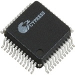
SL811HS Physical Connections These parts are offered in 48-pin TQFP package. The 48-pin TQFP package is the SL811HST-AXC. 48-Pin TQFP Physical Connections 48-Pin TQFP AXC Pin Layout Figure 4. 48-pin TQFP AXC USB Host/Slave Controller Pin Layout NC nRD nDACK* VDD D7 NC [10] NC NC nDRQ* A0 M/S NC 37 1 NC 48 36 NC NC NC nWR NC nCS D6 CM D5 VDD1 48-Pin TQFP D4 Data+ GND Data- D3 USBGnd D2 NC D1 NC NC NC 12 24 NC 25 13 NC Clk/X1 nRST GND NC NC NC VDD X2 INTRQ D0 NC *See Table34 on page22 for Pin and Signal Description for Pins 43 and 44 in Host Mode. The diagram below illustrates a simple +3.3 V voltage source. Figure 5. Sample VDD Generator +5V (USB) R1 45 Ohms 2N2222 Zener +3.3 V (VDD) 3.9v, 1N52288CT- GND Sample VDD Generator Note 10.NC. Indicates No Connection. NC Pins must be left unconnected. Document Number: 38-08008 Rev. *J Page 21 of 39
SL811HS USB Host Controller Pins Description The SL811HST-AXC is packaged in a 48-pin TQFP. These devices require a 3.3 VDC power source and an external 12 or 48 MHz crystal or clock. . Table 34. Pin and Signal Description for Pins 48-Pin TQFP Pin Type Pin Name Pin Description AXC Pin No. 1 NC NC No connection. 2 NC NC No connection. 3 IN nWR Write Strobe Input. An active LOW input used with nCS to write to registers/data memory. 4 IN nCS Active LOW 48-Pin TQFP Chip select. Used with nRD and nWr when accessing the 48-Pin TQFP. 5[11] IN CM Clock Multiply. Select 12 MHz/48 MHz Clock Source. 6 VDD1 +3.3 VDC Power for USB Transceivers. V may be connected to V . DD1 DD 7 BIDIR DATA + USB Differential Data Signal HIGH Side. 8 BIDIR DATA - USB Differential Data Signal LOW Side. 9 GND USB GND Ground Connection for USB. 10 NC NC No connection. 11 NC NC No connection. 12 NC NC No connection. 13 NC NC No connection. 14 NC NC No connection. 15[12] VDD +3.3 VDC Device V Power. DD 16 IN CLK/X1 Clock or External Crystal X1 connection. The X1/X2 Clock requires external 12 or 48 MHz matching crystal or clock source. 17 OUT X2 External Crystal X2 connection. 18 IN nRST Device active low reset input. 19 OUT INTRQ Active HIGH Interrupt Request output to external controller. 20 GND GND Device Ground. 21 BIDIR D0 Data 0. Microprocessor Data/Address Bus. 22 NC NC No connection. 23 NC NC No connection. 24 NC NC No connection. 25 NC NC No connection. 26 NC NC No connection. 27 BIDIR D1 Data 1. Microprocessor Data/Address Bus. 28 BIDIR D2 Data 2. Microprocessor Data/Address Bus. 29 BIDIR D3 Data 3. Microprocessor Data/Address Bus. 30 GND GND Device Ground. 31 BIDIR D4 Data 4. Microprocessor Data/Address Bus. 32 BIDIR D5 Data 5. Microprocessor Data/Address Bus. Notes 11.The CM Clock Multiplier pin must be tied HIGH for a 12 MHz clock source and tied to ground for a 48 MHz clock source. 12.VDD can be derived from the USB supply. See Figure 5 on page 21. Document Number: 38-08008 Rev. *J Page 22 of 39
SL811HS Table 34. Pin and Signal Description for Pins 48-Pin TQFP Pin Type Pin Name Pin Description AXC Pin No. 33 BIDIR D6 Data 6. Microprocessor Data/Address Bus. 34 NC NC No connection. 35 NC NC No connection. 36 NC NC No connection. 37 NC NC No connection. 38 NC NC No connection. 39 BIDIR D7 Data 7. Microprocessor Data/Address Bus. 40 IN M/S Master/Slave Mode Select. ‘1’ selects Slave. ‘0’ = Master. 41 VDD +3.3 VDC Device V Power. DD 42[14] IN A0 A0 = ‘0’. Selects address pointer. Register A0 = ‘1’. Selects data buffer or register. 43 IN nDACK DMA Acknowledge. An active LOW input used to interface to an external DMA controller. DMA is enabled only in slave mode. In host mode, the pin should be tied HIGH (logic ‘1’). 44 OUT nDRQ DMA Request. An active LOW output used with an external DMA controller. nDRQ and nDACK form the handshake for DMA data transfers. In host mode, leave the pin unconnected. 45 IN nRD Read Strobe Input. An active LOW input used with nCS to read registers/data memory. 46 NC NC No connection. 47 NC NC No connection. 48 NC NC No connection. Figure 6. Package Markings (48-Pin TQFP) Notes 13.VDD can be derived from the USB supply. Figure 5 on page 21 shows a simple method to provide 3.3 V/30 mA. Another option is to use a Torex Semiconductor, Ltd. 3.3 V SMD regulator (part number XC62HR3302MR). 14.The A0 Address bit is used to access address register or data registers in I/O Mapped or Memory Mapped applications. Document Number: 38-08008 Rev. *J Page 23 of 39
SL811HS Electrical Specifications Absolute Maximum Ratings This section lists the absolute maximum ratings of the SL811HS. Exceeding maximum ratings may shorten the useful life of the device. User guidelines are not tested. Description Condition Storage Temperature –40 °C to 125 °C Voltage on any pin with respect to ground –0.3 V to 6.0 V Power Supply Voltage (V ) 4.0 V DD Power Supply Voltage (V ) 4.0 V DD1 Lead Temperature (10 seconds) 180°C Recommended Operating Conditions Parameter Min Typical Max Power Supply Voltage, VDD 3.0 V 3.3 V 3.45 V Power Supply Voltage, VDD1 3.0 V 3.45 V Operating Temperature 0 °C 65 °C Crystal Requirements, Min Typical Max (X1, X2) Operating Temperature Range 0°C 65 °C Parallel Resonant Frequency 48 MHz Frequency Drift over Temperature ±50 ppm Accuracy of Adjustment ±30 ppm Series Resistance 100 Ohms Shunt Capacitance 3 pF 6 pF Load Capacitance 20 pF Drive Level 20 W 5 mW Mode of Vibration Third Overtone[15] External Clock Input Characteristics (X1) Parameter Min Typical Max Clock Input Voltage at X1 (X2 Open) 1.5 V Clock Frequency[16] 48 MHz Notes 15.Fundamental mode for 12 MHz Crystal. 16.The SL811HS can use a 12 MHz Clock Source. Document Number: 38-08008 Rev. *J Page 24 of 39
SL811HS DC Characteristics Parameter Description Min Typ Max V Input Voltage LOW –0.3 V 0.8 V IL V Input Voltage HIGH (5 V Tolerant I/O) 2.0 V 6.0 V IH V Output Voltage LOW (I = 4 mA) 0.4 V OL OL V Output Voltage HIGH (I = –4 mA) 2.4 V OH OH I Output Current HIGH 4 mA OH I Output Current LOW 4 mA OL I Input Leakage ±1 A LL C Input Capacitance 10 pF IN I [17] Supply Current (V ) inc USB at FS 21 mA 25 mA CC DD I [18] Supply Current (V ) Suspend w/Clk & Pll Enb 4.2 mA 5 mA CCsus1 DD I [19] Supply Current (V ) Suspend no Clk & Pll Dis 50 A 60 A CCsus2 DD I Supply Current (V ) 10 mA USB DD1 I Transceiver Supply Current in Suspend 10 A USBSUS USB Host Transceiver Characteristics Parameter Description Min Typ[20] Max V Differential 0.2 V 200 mV IHYS Input Sensitivity (Data+, Data–) V USB Input Voltage HIGH Driven 2.0 V USBIH V USB Input Voltage LOW 0.8 V USBIL V USB Output Voltage HIGH 2.0 V USBOH V USB Output Voltage LOW 0.0 V 0.3 V USBOL Z [21] Output Impedance HIGH STATE 36 Ohms 42 Ohms USBH Z [21] Output Impedance LOW STATE 36 Ohms 42 Ohms USBL I Transceiver Supply p-p Current (3.3 V) 10 mA USB at FS Every V pin, including USB V , must have a decoupling capacitor to ensure clean V (free of high frequency noise) at the chip DD DD DD input point (pin) itself. The best way to do this is to connect a ceramic capacitor (0.1F, 6 V) between the pin itself and a good ground. Keep capacitor leads as short as possible. Use surface mount capacitors with the shortest traces possible (the use of a ground plane is strongly recom- mended). This product was tested as compliant to the USB-IF specification under the test identification number (TID) of 40000689 and is listed on the USB-IF’s integrators list. Notes 17.ICC measurement includes USB Transceiver current (IUSB) operating at full speed. 18.ICCsus1 measured with 12 MHz Clock Input and Internal PLL enabled. Suspend set –(USB transceiver and internal Clocking disabled). 19.ICCsus2 measured with external Clock, PLL disabled, and Suspend set. For absolute minimum current consumption, ensure that all inputs to the device are at static logic level. 20.All typical values are VDD = 3.3 V and TAMB= 25°C. 21.ZUSBX impedance values includes an external resistor of 24 Ohms ± 1% (SL811HS revision 1.2 requires external resistor values of 33 Ohms ±1%). Document Number: 38-08008 Rev. *J Page 25 of 39
SL811HS Bus Interface Timing Requirements I/O Write Cycle twr twrhigh nWR twasu twahld A0 twdsu twdsu twdhld twdhld Register or Memory D0-D7 DATA Address twcsu twshld nCS Tcscs See Note. I/O Write Cycle to Register or Memory Buffer Parameter Description Min Typ Max t Write pulse width 85 ns WR t Chip select set-up to nWR LOW 0 ns WCSU t Chip select hold time 0 ns WSHLD After nWR HIGH t A0 address setup time 85 ns WASU t A0 address hold time 10 ns WAHLD t Data to Write HIGH set-up time 85 ns WDSU t Data hold time after Write HIGH 5 ns WDHLD t nCS inactive to nCS* asserted 85 ns CSCS t NWR HIGH 85 ns WRHIGH Note nCS an be held LOW for multiple Write cycles provided nWR is cycled. Write Cycle Time for Auto Inc Mode Writes is 170 ns minimum. Document Number: 38-08008 Rev. *J Page 26 of 39
SL811HS I/O Read Cycle twr twrrdl nWR twasu twahld A0 trdp nRD tracc trdhld twdsu twdhld Register or Memory D0-D7 Address DATA trcsu trshld nCS Tcscs *Note I/O Read Cycle from Register or Memory Buffer Parameter Description Min Typ Max t Write pulse width 85 ns WR t Read pulse width 85 ns RD t Chip select set-up to nWR 0 ns WCSU t A0 address set-up time 85 ns WASU t A0 address hold time 10 ns WAHLD t Data to Write HIGH set-up time 85 ns WDSU t Data hold time after Write HIGH 5 ns WDHLD t Data valid after Read LOW 25 ns 85 ns RACC t Data hold after Read HIGH 40 ns RDHLD t Chip select LOW to Read LOW 0 ns RCSU t NCS hold after Read HIGH 0 ns RSHLD T * nCS inactive to nCS *asserted 85 ns CSCS t nWR HIGH to nRD LOW 85ns WRRDL Note nCS can be kept LOW during multiple Read cycles provided nRD is cycled. Rd Cycle Time for Auto Inc Mode Reads is 170 ns minimum. Document Number: 38-08008 Rev. *J Page 27 of 39
SL811HS DMA Write Cycle tdakrq tackrq nDRQ tdack nDACK tdwrlo D0-D7 DATA tdsu tdwrp tdhld nWR tackwrh DMA Write Cycle SL811 DMA WRITE CYCLE TIMING Parameter Description Min Typ Max tdack nDACK low 80 ns tdwrlo nDACK to nWR low delay 5 ns tdakrq nDACK low to nDRQ high delay 5 ns tdwrp nWR pulse width 65 ns tdhld Data hold after nWR high 5 ns tdsu Data set-up to nWR strobe low 60 ns tackrq NDACK high to nDRQ low 5 ns tackwrh NDACK high to nDRQ low 5 ns twrcycle DMA Write Cycle Time 150 ns Note nWR must go low after nDACK goes low in order for nDRQ to clear. If this sequence is not implemented as requested, the next nDRQ is not inserted. Document Number: 38-08008 Rev. *J Page 28 of 39
SL811HS DMA Read Cycle nDRQ tdckdr tdakrq tdack nDACK tddrdlo D0-D7 DATA tdaccs tdhld tdrdp nRD SL811 DMA Read Cycle Timing SL811 DMA READ CYCLE TIMING Parameter Description Min Typ Max tdack nDACK low 100 ns tddrdlo nDACK to nRD low delay 0 ns tdckdr nDACK low to nDRQ high delay 5 ns tdrdp nRD pulse width 90 ns tdhld Date hold after nDACK high 5 ns tddaccs Data access from nDACK low 85 ns tdrdack nRD high to nDACK high 0 ns tdakrq nDRQ low after nDACK high 5 ns trdcycle DMA Read Cycle Time 150 ns Note Data is held until nDACK goes high regardless of state of nREAD. Reset Timing treset nRST tioact nRD or nWR Reset Timing Parameter Description Min Typ Max t nRst Pulse width 16 clocks RESET t nRst HIGH to nRD or nWR active 16 clocks IOACT Note Clock is 48 MHz nominal. Document Number: 38-08008 Rev. *J Page 29 of 39
SL811HS Clock Timing Specifications tclk tlow CLK thigh tfall trise CCLlOocCkK T iTmIiMngING Parameter Description Min Typ Max t Clock Period (48 MHz) 20.0 ns 20.8 ns CLK t Clock HIGH Time 9 ns 11 ns HIGH t Clock LOW Time 9 ns 11 ns LOW t Clock Rise Time 5.0 ns RISE t Clock Fall Time 5.0 ns FALL Clock Duty Cycle 45% 55% Ordering Information Part Number Package Type SL811HST-AXC 48-pin Pb-free – Ordering Code Definitions SL811 HST - A X C Temperature range: C = Commercial X = Pb-free Package Type: TQFP Host/slave Part number Document Number: 38-08008 Rev. *J Page 30 of 39
SL811HS Package Diagram Figure 7. 48-pin TQFP (7 × 7 × 1.4 mm) Package Outline, 51-85135 51-85135 *C Document Number: 38-08008 Rev. *J Page 31 of 39
SL811HS Acronyms Document Conventions Table 35. Acronyms Used in this Document Units of Measure Acronym Description Table 36. Units of Measure CMOS Complementary Metal Oxide Semiconductor Symbol Unit of Measure CPU Central Processing Unit mA milliampere CRC Cyclical Redundancy Check Mbps megabits per second DMA Direct Memory Access MHz megahertz mV millivolt DPLL Dynamic Phase Locked Loop mW milliwatt I/O Input Output ns nanosecond PCMCIA Personal Computer Memory Card International Association ppm parts per million RAM Random Access Memory pF picofarad V volt SIE Serial Interface Engine VDC volts (direct current) SOF Start of Frame SRAM Static Random Access Memory USB Universal Serial Bus Document Number: 38-08008 Rev. *J Page 32 of 39
SL811HS Errata This section describes the errata for the SL811HS. Details include errata trigger conditions, available workaround, and silicon revision applicability. Contact your local Cypress Sales Representative if you have questions. Part Numbers Affected Part Number Package Type Operating Range SL811HS All Commercial SL811HS/SL811 Qualification Status Product status: In production - Qual Report: 014401 SL811HS/SL811 Errata Summary The following table defines the errata applicability to available SL811HS/SL811 family of devices. Note Errata titles in this table are hyperlinked. Click an entry to go to its description. Items SL811HS/SL811S Rev Letter/Number Fix Status 1. Host Mode: SE0 problem in low-speed hub operation X 1.5 Use workaround 2. Host Mode: Sync to SOF does not apply to low-speed mode X 1.5 Use workaround 3. Host/Peripheral Mode: 12 MHz operation with sensitive in- X 1.5 Use workaround ternal PLL 4. Peripheral Mode: Unreliable DMA interface X 1.5 Use workaround 5. Peripheral Mode: SL811HS can miss packets in a noisy X 1.5 Use workaround environment 6. Host/Peripheral Mode: Auto-increment feature results in X 1.5 Use workaround corrupt data 1.Host Mode: SEO problem in low-speed hub operation ■Problem Definition Some hubs that send SE0s upstream during the EOF1 time frame may cause the SL811HS to stop sending SOFs. This problem occurs when operating with low-speed devices attached downstream of such a hub. This is not a problem with full-speed devices. According to the USB Specification, hubs are permitted to transmit SE0s during the EOF1 time frame. This is done to eliminate potential babble conditions on the bus and is an optional feature implemented in some hubs. ■Parameters Affected SOFs ■Trigger Condition(S) Attaching hub that sends SE0s upstream during the EOF1 time frame. ■Scope of Impact The SL811HS can not host a low-speed device downstream of a hub that generates SE0s during EOF1. ■Workaround The only complete workaround is to use a hub that does not transmit SE0s upstream during EOF1. Some hubs, including all Cypress hubs, have the option to disable SE0s from being generated during EOF1. For a list of hubs that do not generate SE0s upstream during EOF1, or for more information on disabling this feature in Cypress hubs, contact Cypress USB support. ■Fix Status Use workaround. Document Number: 38-08008 Rev. *J Page 33 of 39
SL811HS 2.Host Mode: Sync to SOF does not apply to low-speed mode ■Problem Definition The SYNC to SOF bit (bit 5) of the USB Host Control Registers [00H, 08H], is only designed for full-speed support. However, all other full-speed SOF bits and registers do apply to low-speed EOPs as well. In full-speed mode, this bit should only be used when the software cannot fit a packet within the remaining 1 ms frame. Setting this bit automatically delays sending the packet until the next SOF. ■Parameters Affected SYNC to SOF ■Trigger Condition(S) Full-speed support. ■Scope of Impact If the SOF bit is set when operating in low-speed mode, packets may not get sent from the SL811HS. ■Workaround Do not set the SOF bit when operating in low-speed mode. Instead, if a packet does not fit within the remaining 1 ms frame, firmware needs to delay sending it until after the next EOP. Using a simple delay loop or using the SOF timer interrupt (also EOP timer interrupt in low-speed mode) are two possible ways of doing this. ■Fix Status Use workaround. 3.Host/Peripheral Mode: 12 MHz operation with sensitive internal PLL ■Problem Definition The internal PLL is very sensitive. The PLL causes any high frequency noise on the V pins to result in clock jitter. DD ■Parameters Affected USB data signaling at full-speed and improper timing of SOF packets. ■Trigger Condition(S) Operation at 12 MHz with high frequency noise on the V pins. DD ■Scope of Impact When operating the SL811HS at 12 MHz, high frequency noise on the V pins can result in clock jitter. The clock jitter results in DD different symptoms depending on the severity of the jitter. Most notable is improper USB data signaling at full speed and improper timing of SOF packets. ■Workaround The best workaround is to use 48 MHz to eliminate using the PLL. If 12 MHz is required, take these steps to reduce any jitter output of the PLL. 1. Reduce high frequency noise on all SL811HS V pins. This can be accomplished by adding proper decoupling capacitors DD directly on the V pins. The value of 0.1 µF can be too large, depending on the inductivity of the traces on the PCB; experiment DD with values of 0.01 µF or even 1000 pF. In addition, ceramic capacitors are recommended. 2. Use a 12 MHz oscillator instead of a crystal. An oscillator produces much sharper edge rates, which allow more tolerance for jitter. 3. Careful layout can minimize this PLL jitter significantly: a. Use the shortest traces possible for decoupling capacitors. b. Use ground and VCC planes. ■Fix Status Use workaround. Document Number: 38-08008 Rev. *J Page 34 of 39
SL811HS 4.Peripheral Mode: Unreliable DMA interface ■Problem Definition The DMA interface can be unreliable in slave mode. ■Parameters Affected DMA transfers to or from the SL811HS internal RAM. ■Trigger Condition(S) Use of the DMA interface to move data to or from SL811HS internal RAM. ■Scope of Impact When performing DMA writes, data may get corrupted. This problem has only been seen for DMA write operations, but can also occur for read operations as well. ■Workaround Use the standard Data Port interface instead of the DMA interface for writing to or reading from the SL811HS RAM space. The DMA interface is not a recommended interface for the SL811HS due to this issue. ■Fix Status Use workaround. 5.Peripheral Mode: SL811HS can miss packets in a noisy environment ■Problem Definition In a noisy environment, the SL811HS has the potential to occasionally miss a packet. Occasionally missed packets are anticipated and dealt with in USB 2.0 Specification Section 10.2.6, where the following applies “It is recommended that the error count not be incremented when there is an error due to host specific reasons (buffer underrun or overrun), and that whenever a transaction does not encounter a transmission error, the error count be reset to zero.” In other words if an individual packet is missed and the next packet is processed properly, the recommendation is that the error counter be reset to ‘0’. When drivers are written with this in mind, they can avoid issues that cause the transfer to be retired due to three errors in a transaction. ■Parameters Affected Error count. ■Trigger Condition(S) Electrically noisy environments. ■Scope of Impact If the SL811HS is used in an electrically noisy environment that may corrupt three requests within that transaction, the transaction will be retired by the host. ■Workaround 1) The workaround for this issue is to write the driver according to the guidelines specified in section 10.2.6 of the USB 2.0 Specification, to prevent the driver from retrying the transfer. 2) Board layout is the major reason for electrical noise that can aggravate this issue. When doing layout for the USB chip, use guidelines provided in a Cypress application note titled, High-speed USB PCB Layout Recommendations found on the Cypress web site. ■Fix Status Use workaround. Document Number: 38-08008 Rev. *J Page 35 of 39
SL811HS 6.Host/Peripheral Mode: Auto-increment feature results in corrupt data ■Problem Definition The SL811HS has a feature called auto-increment used to read or write blocks of the data buffer. This feature is used to speed up the time it takes to write blocks of data because an address location write is not required between data writes or reads. In some cases, the auto-increment feature can intermittently fail, causing the RAM location to be corrupted or the read buffer to provide incorrect data to the system processor. This type of error is very infrequent. ■Parameters Affected Any RAM location where auto-increment feature is used to access data. This includes both register and buffer space. ■Trigger Condition(S) Use of the auto-increment feature. ■Scope of Impact When using the auto-increment feature for writes or reads, it is possible for the data to become corrupt. The following table demonstrates a typical error when it occurs. The error condition is shown in red. If an error occurs during writes using auto-increment, an address location can be written with the value of the previous address; each subsequent write will also be incorrect until the end of the block write. In the following example, note that the value of 0x01 from address 0x11 is incorrectly written to address 0x12 instead of the expected value of 0x02. After this error, the write to each subsequent address is also incorrectly written with the value that was intended to be in the previous address location. If an error occurs during a read using auto-increment, a single location can be incorrectly read as the previous addresses value. If the data is read again, it will show that the data in RAM is correct. Auto-increment error during a write Address 0x10 0x11 0x12 0x13 0x14 ...... 0x1E 0x1F Data intended to be written to RAM 0x00 0x01 0x02 0x03 0x04 ..... 0x0E 0x0F Data actually written to RAM 0x00 0x01 0x01 0x02 0x03 ..... 0x0D 0x0E Auto-increment error during a read Address 0x10 0x11 0x12 0x13 0x14 ...... 0x1E 0x1F Data actually in RAM 0x00 0x01 0x02 0x03 0x04 ..... 0x0E 0x0F Data read back from RAM 0x00 0x01 0x01 0x03 0x04 ..... 0x0E 0x0F ■Workaround The easiest way to work around this issue is to not use the auto-increment feature. This affects performance because the address must be written prior to each write or read. ■Fix Status Use workaround. Document Number: 38-08008 Rev. *J Page 36 of 39
SL811HS Document History Page Document Title: SL811HS, Embedded USB Host/Slave Controller Document Number: 38-08008 Submission Orig. of Revision ECN Description of Change Date Change ** 110850 12/14/01 BHA Converted to Cypress format from ScanLogic *A 112687 03/22/02 MUL 1) Changed power supply voltage to 4.0 V in section 7.1 2) Changed value of twdsu in section 7.6.2 3) Changed max. power supply voltage to 3.45 V in section 7.2 4) Changed accuracy of adjustment in section 7.2 5) Changed bits 0 and 1 to reserved in section 5.3.8 6) Changed bit 2 to reserved in section 5.3.5 and 5.3.7 7) Changed bit 2 to reserved in section 5.3.1 8) Changed definition of bit 6 in section 5.3.5 & 5.3.7 9) Added section 5.1, Register Values on Power-up and Reset 10) Changed bit description notes in section 5.3.7 11) Changed note about series termination resistors in section 7.5 12) Changed example in section 5.3.9 13) Changed J-K Programming States table in section 5.3.2 14) Added and removed comments for low-power modes in section 5.3.4 15) Removed sections specific to slave operation and SL11H 16) Removed duplicate tables 17) General formatting changes to section headings 18) Fixed all part number references 19) Added comments to section 7.5 and new definitions to section 2.0 *B 381894 See ECN VCS Went from single column to 2-column format. Combined information from SL811HS (38-08008) and SL811S/T (83-08009) *C 464641 See ECN ARI Added lead free part numbers to new section Ordering Information and corrected references made to these parts. Corrected grammar. Added compliance statement in section USB Host Transceiver Characteristics. *D 749518 See ECN ARI Implemented the new template. Changed Figure 4. Labels on pins 2 and 3 were swapped; this has been corrected. Combined the 48-pin TQFP AXC Pin Assignment and Definition table with the 28-pin PLCC Pin Assignment and Definition table. Removed all instances of SL811HST-AC. Corrected the variables. Removed references to the obsolete SL11H. *E 2914091 04/15/2010 VRD Removed inactive parts from Ordering Information. Updated Packaging Information. *F 3202147 03/22/11 ODC Template and style updates. Added ordering code definitions, acronyms and units of measure. Updated table titles and references. Removed all references to 28-pin PLCC Package information as the package is no longer offered. Removed figure “Package Markings (28-pin PLCC)” on page 21 as it refers the PLCC package. Removed figure “48-Pin TQFP Mechanical Dimensions” as this is a duplicate of the Package diagram later in the spec on page 31. Document Number: 38-08008 Rev. *J Page 37 of 39
SL811HS Document History Page (continued) Document Title: SL811HS, Embedded USB Host/Slave Controller Document Number: 38-08008 Submission Orig. of Revision ECN Description of Change Date Change *G 3999512 07/26/2013 PRVE Added Errata footnote (Note 1, 2, 3, 4, 6, 7). Updated Functional Overview: Updated Data Port, Microprocessor Interface: Added Note 1 and referred the same note in “SL811HS”. Added Note 2 and referred the same note in “DMA bidirectional interface in slave mode”. Updated Buffer Memory: Updated Auto Address Increment Mode [3] Added Note 3 and referred the same note in the heading. Updated PLL Clock Generator: Added Note 4 and referred the same note in “12 MHz”. Updated USB Transceiver: Added Note 6 and referred the same note in “full speed”. Added Note 7 and referred the same note in “low speed”. Added Errata. Updated to new template. *H 4346004 04/14/2014 PRVE Updated Package Diagram: spec 51-85135 – Changed revision from *B to *C. Completing Sunset Review. *I 5725314 05/03/2017 PRVE Updated to new template. Completing Sunset Review. *J 5840358 08/01/2017 SRDR Updated Package Markings (48-Pin TQFP). Document Number: 38-08008 Rev. *J Page 38 of 39
SL811HS Sales, Solutions, and Legal Information Worldwide Sales and Design Support Cypress maintains a worldwide network of offices, solution centers, manufacturer’s representatives, and distributors. To find the office closest to you, visit us at Cypress Locations. Products PSoC® Solutions ARM® Cortex® Microcontrollers cypress.com/arm PSoC 1 | PSoC 3 | PSoC 4 | PSoC 5LP Automotive cypress.com/automotive Cypress Developer Community Clocks & Buffers cypress.com/clocks Forums | WICED IOT Forums | Projects | Video | Blogs | Interface cypress.com/interface Training | Components Internet of Things cypress.com/iot Technical Support Memory cypress.com/memory cypress.com/support Microcontrollers cypress.com/mcu PSoC cypress.com/psoc Power Management ICs cypress.com/pmic Touch Sensing cypress.com/touch USB Controllers cypress.com/usb Wireless Connectivity cypress.com/wireless © Cypress Semiconductor Corporation, 2001–2017. This document is the property of Cypress Semiconductor Corporation and its subsidiaries, including Spansion LLC ("Cypress"). This document, including any software or firmware included or referenced in this document ("Software"), is owned by Cypress under the intellectual property laws and treaties of the United States and other countries worldwide. Cypress reserves all rights under such laws and treaties and does not, except as specifically stated in this paragraph, grant any license under its patents, copyrights, trademarks, or other intellectual property rights. If the Software is not accompanied by a license agreement and you do not otherwise have a written agreement with Cypress governing the use of the Software, then Cypress hereby grants you a personal, non-exclusive, nontransferable license (without the right to sublicense) (1) under its copyright rights in the Software (a) for Software provided in source code form, to modify and reproduce the Software solely for use with Cypress hardware products, only internally within your organization, and (b) to distribute the Software in binary code form externally to end users (either directly or indirectly through resellers and distributors), solely for use on Cypress hardware product units, and (2) under those claims of Cypress's patents that are infringed by the Software (as provided by Cypress, unmodified) to make, use, distribute, and import the Software solely for use with Cypress hardware products. Any other use, reproduction, modification, translation, or compilation of the Software is prohibited. TO THE EXTENT PERMITTED BY APPLICABLE LAW, CYPRESS MAKES NO WARRANTY OF ANY KIND, EXPRESS OR IMPLIED, WITH REGARD TO THIS DOCUMENT OR ANY SOFTWARE OR ACCOMPANYING HARDWARE, INCLUDING, BUT NOT LIMITED TO, THE IMPLIED WARRANTIES OF MERCHANTABILITY AND FITNESS FOR A PARTICULAR PURPOSE. To the extent permitted by applicable law, Cypress reserves the right to make changes to this document without further notice. Cypress does not assume any liability arising out of the application or use of any product or circuit described in this document. Any information provided in this document, including any sample design information or programming code, is provided only for reference purposes. It is the responsibility of the user of this document to properly design, program, and test the functionality and safety of any application made of this information and any resulting product. Cypress products are not designed, intended, or authorized for use as critical components in systems designed or intended for the operation of weapons, weapons systems, nuclear installations, life-support devices or systems, other medical devices or systems (including resuscitation equipment and surgical implants), pollution control or hazardous substances management, or other uses where the failure of the device or system could cause personal injury, death, or property damage ("Unintended Uses"). A critical component is any component of a device or system whose failure to perform can be reasonably expected to cause the failure of the device or system, or to affect its safety or effectiveness. Cypress is not liable, in whole or in part, and you shall and hereby do release Cypress from any claim, damage, or other liability arising from or related to all Unintended Uses of Cypress products. You shall indemnify and hold Cypress harmless from and against all claims, costs, damages, and other liabilities, including claims for personal injury or death, arising from or related to any Unintended Uses of Cypress products. Cypress, the Cypress logo, Spansion, the Spansion logo, and combinations thereof, WICED, PSoC, CapSense, EZ-USB, F-RAM, and Traveo are trademarks or registered trademarks of Cypress in the United States and other countries. For a more complete list of Cypress trademarks, visit cypress.com. Other names and brands may be claimed as property of their respective owners. Document Number: 38-08008 Rev. *J Revised August 1, 2017 Page 39 of 39
Mouser Electronics Authorized Distributor Click to View Pricing, Inventory, Delivery & Lifecycle Information: C ypress Semiconductor: SL811HST-AXC