ICGOO在线商城 > 集成电路(IC) > 嵌入式 - 微控制器 - 应用特定 > CYUSB3014-BZXC
 Datasheet下载
- 型号: CYUSB3014-BZXC
- 制造商: Cypress Semiconductor
- 库位|库存: xxxx|xxxx
- 要求:
| 数量阶梯 | 香港交货 | 国内含税 |
| +xxxx | $xxxx | ¥xxxx |
查看当月历史价格
查看今年历史价格
CYUSB3014-BZXC产品简介:
ICGOO电子元器件商城为您提供CYUSB3014-BZXC由Cypress Semiconductor设计生产,在icgoo商城现货销售,并且可以通过原厂、代理商等渠道进行代购。 CYUSB3014-BZXC价格参考。Cypress SemiconductorCYUSB3014-BZXC封装/规格:嵌入式 - 微控制器 - 应用特定, 。您可以下载CYUSB3014-BZXC参考资料、Datasheet数据手册功能说明书,资料中有CYUSB3014-BZXC 详细功能的应用电路图电压和使用方法及教程。
CYUSB3014-BZXC是Cypress Semiconductor Corp(现为英飞凌科技公司的一部分)推出的一款应用特定型嵌入式微控制器,属于EZ-USB FX3系列。该芯片主要面向需要高速USB 3.0接口的数据传输应用。

其核心应用场景包括:高清视频采集与传输设备(如工业摄像头、医疗影像设备、无人机图传系统)、机器视觉系统、数字标牌、测试测量仪器以及需要大带宽数据传输的外设设备。CYUSB3014-BZXC集成了USB 3.0外设控制器和可编程ARM9处理器,支持高达5 Gbps的传输速率,能够实现从FPGA、传感器或图像处理器到主机PC的高效、低延迟数据传输。

此外,该芯片广泛用于需要将并行或串行数据流桥接至USB 3.0接口的系统中,典型应用包括FPGA到PC的数据回传、高速数据采集系统和智能摄像头模块。其灵活的GPIF II(通用可编程接口)可无缝连接多种处理器、ASIC或FPGA,大大简化系统设计。

由于具备高可靠性、低功耗和强大的接口扩展能力,CYUSB3014-BZXC在工业自动化、科研设备和嵌入式视觉领域具有重要地位。开发者可通过Cypress提供的SDK和开发工具快速完成固件开发与调试,加快产品上市时间。总之,该器件适用于对数据吞吐量和实时性要求较高的专业级嵌入式应用。
| 参数 | 数值 |
| 产品目录 | 集成电路 (IC)半导体 |
| 描述 | IC ARM9 USB3 CONTROLLER 121FBGAUSB 接口集成电路 EZUSB SuperSpeedCtrl X32 256KB |
| 产品分类 | |
| I/O数 | 60 |
| 品牌 | Cypress Semiconductor Corp |
| 产品手册 | |
| 产品图片 |
|
| rohs | 符合RoHS无铅 / 符合限制有害物质指令(RoHS)规范要求 |
| 产品系列 | 接口 IC,USB 接口集成电路,Cypress Semiconductor CYUSB3014-BZXCEZ-USB FX3™ |
| 数据手册 | http://www.cypress.com/?docID=50647 |
| 产品型号 | CYUSB3014-BZXC |
| RAM容量 | 512K x 8 |
| 产品种类 | USB 接口集成电路 |
| 供应商器件封装 | - |
| 其它名称 | 428-3182 |
| 包装 | 托盘 |
| 商标 | Cypress Semiconductor |
| 商标名 | EZ-USB |
| 安装类型 | - |
| 安装风格 | SMD/SMT |
| 封装 | Tray |
| 封装/外壳 | 121-TFBGA |
| 封装/箱体 | BGA-121 |
| 工作温度 | 0°C ~ 70°C |
| 工作电源电压 | 3.2 V to 6 V |
| 工厂包装数量 | 168 |
| 应用 | USB 主机/外围设备控制器 |
| 接口 | GPIF, I²C, I²S, SPI, UART, USB |
| 接口类型 | I2C, I2S, SPI, UART, USB |
| 控制器系列 | CYUSB |
| 标准 | USB 3.0 |
| 标准包装 | 168 |
| 核心处理器 | ARM9® |
| 特色产品 | http://www.digikey.cn/product-highlights/cn/zh/cypress-ez-usb-fx3-usb-controller/3232 |
| 电压-电源 | 1.15 V ~ 1.25 V |
| 程序存储器类型 | 外部程序存储器 |
| 类型 | Controller |
| 系列 | EZ-USB FX3 |
| 速度 | SuperSpeed |


- 商务部:美国ITC正式对集成电路等产品启动337调查
- 曝三星4nm工艺存在良率问题 高通将骁龙8 Gen1或转产台积电
- 太阳诱电将投资9.5亿元在常州建新厂生产MLCC 预计2023年完工
- 英特尔发布欧洲新工厂建设计划 深化IDM 2.0 战略
- 台积电先进制程称霸业界 有大客户加持明年业绩稳了
- 达到5530亿美元!SIA预计今年全球半导体销售额将创下新高
- 英特尔拟将自动驾驶子公司Mobileye上市 估值或超500亿美元
- 三星加码芯片和SET,合并消费电子和移动部门,撤换高东真等 CEO
- 三星电子宣布重大人事变动 还合并消费电子和移动部门
- 海关总署:前11个月进口集成电路产品价值2.52万亿元 增长14.8%

PDF Datasheet 数据手册内容提取
CYUSB301X/CYUSB201X ® EZ-USB FX3: SuperSpeed USB Controller EZ-USB® FX3: SuperSpeed USB Controller Features ❐Includes RTOS Framework (using ThreadX Version 5) ❐Firmware examples covering all I/O modules ■Universal serial bus (USB) integration ❐Visual Studio host examples using C++ and C# ❐USB 3.1, Gen 1 and USB 2.0 peripherals compliant with USB ■SuperSpeed Explorer Board available for rapid prototyping 3.1 Specification Revision 1.0 (TID # 340800007) ❐Several accessory boards also available: ❐5-Gbps SuperSpeed PHY compliant with USB 3.1 Gen 1 • Adapter boards for Xilinx/Altera FPGA development ❐High-speed On-The-Go (HS-OTG) host and peripheral compliant with OTG Supplement Version 2.0 • Adapter board for Video development ❐Thirty-two physical endpoints • CPLD board for concept testing and initial development ❐Support for battery charging Specification 1.1 and accessory Applications charger adaptor (ACA) detection ■General Programmable Interface (GPIF™ II) ■Digital video camcorders ❐Programmable 100-MHz GPIF II enables connectivity to a ■Digital still cameras wide range of external devices ❐8-, 16-, 24-, and 32-bit data bus ■Printers ❐Up to16 configurable control signals ■Scanners ■Fully accessible 32-bit CPU ■Video capture cards ❐ARM926EJ core with 200-MHz operation ❐512-KB or 256-KB embedded SRAM ■Test and measurement equipment ■Additional connectivity to the following peripherals ■Surveillance cameras ❐SPI master at up to 33 MHz ■Personal navigation devices ❐UART support of up to 4 Mbps ❐I2C master controller at 1 MHz ■Medical imaging devices ❐I2S master (transmitter only) at sampling frequencies of ■Video IP phones 32kHz, 44.1kHz, and 48kHz ■Portable media players ■Selectable clock input frequencies ❐19.2, 26, 38.4, and 52 MHz ■Industrial cameras ❐19.2-MHz crystal input support ■Data loggers ■Ultra low-power in core power-down mode ■Data acquisition ❐Less than 60 µA with VBATT on and 20 µA with VBATT off ■High-performance Human Interface Devices (gesture ■Independent power domains for core and I/O recognition) ❐Core operation at 1.2 V ❐I2S, UART, and SPI operation at 1.8 to 3.3 V Functional Description ❐I2C operation at 1.2 V to 3.3 V For a complete list of related documentation, click here. ■Package options ❐121-ball, 10- × 10-mm, 0.8-mm pitch Pb-free ball grid array (BGA) ❐See Table20 for details on the seven FX3 variants ■EZ-USB® Software Development Kit (SDK) for code devel- opment of firmware and PC Applications CypressSemiconductorCorporation • 198 Champion Court • SanJose, CA 95134-1709 •408-943-2600 Document Number: 001-52136 Rev. *V Revised February 19, 2018
CYUSB301X/CYUSB201X Logic Block Diagram Document Number: 001-52136 Rev. *V Page 2 of 53
CYUSB301X/CYUSB201X More Information Cypress provides a wealth of data at www.cypress.com to help you to select the right <product> device for your design, and to help you to quickly and effectively integrate the device into your design. For a comprehensive list of resources, see the knowledge base article KBA87889, How to design with FX3/FX3S. ■Overview: USB Portfolio, USB Roadmap ❐AN73609 - EZ-USB FX2LP/ FX3 Developing Bulk-Loop Ex- ample on Linux ■USB 3.0 Product Selectors: FX3, FX3S, CX3, HX3, West Bridge Benicia ❐AN77960 - Introduction to EZ-USB FX3 High-Speed USB Host Controller ■Application notes: Cypress offers a large number of USB appli- ❐AN76348 - Differences in Implementation of EZ-USB FX2LP cation notes covering a broad range of topics, from basic to and EZ-USB FX3 Applications advanced level. Recommended application notes for getting ❐AN89661 - USB RAID 1 Disk Design Using EZ-USB FX3S started with FX3 are: ❐AN75705 - Getting Started with EZ-USB FX3 ■Code Examples: < Modify as required > ❐AN76405 - EZ-USB FX3 Boot Options ❐USB Hi-Speed ❐AN70707 - EZ-USB FX3/FX3S Hardware Design Guidelines ❐USB Full-Speed and Schematic Checklist ❐USB SuperSpeed ❐AN65974 - Designing with the EZ-USB FX3 Slave FIFO In- ■Technical Reference Manual (TRM): terface ❐EZ-USB FX3 Technical Reference Manual ❐AN75779 - How to Implement an Image Sensor Interface with EZ-USB FX3 in a USB Video Class (UVC) Framework ■Development Kits: ❐AN86947 - Optimizing USB 3.0 Throughput with EZ-USB ❐CYUSB3KIT-003, EZ-USB FX3 SuperSpeed Explorer Kit FX3 ❐CYUSB3KIT-001, EZ-USB FX3 Development Kit ❐AN84868 - Configuring an FPGA over USB Using Cypress EZ-USB FX3 ■Models: IBIS ❐AN68829 - Slave FIFO Interface for EZ-USB FX3: 5-Bit Ad- dress Mode EZ-USB FX3 Software Development Kit Cypress delivers the complete software and firmware stack for FX3, in order to easily integrate SuperSpeed USB into any embedded application. The Software Development Kit (SDK) comes with tools, drivers and application examples, which help accelerate appli- cation development. GPIF™ II Designer The GPIF II Designer is a graphical software that allows designers to configure the GPIF II interface of the EZ-USB FX3 USB 3.0 Device Controller. The tool allows users the ability to select from one of five Cypress supplied interfaces, or choose to create their own GPIF II interface from scratch. Cypress has supplied industry standard interfaces such as Asynchronous and Synchronous Slave FIFO, Asynchronous and Synchronous SRAM, and Asynchronous SRAM. Designers who already have one of these pre-defined interfaces in their system can simply select the interface of choice, choose from a set of standard parameters such as bus width (x8, 16, x32) endianess, clock settings, and compile the interface. The tool has a streamlined three step GPIF interface development process for users who need a customized interface. Users are able to first select their pin configuration and standard parameters. Secondly, they can design a virtual state machine using configurable actions. Finally, users can view output timing to verify that it matches the expected timing. Once the three step process is complete, the interface can be compiled and integrated with FX3. Document Number: 001-52136 Rev. *V Page 3 of 53
CYUSB301X/CYUSB201X Contents Functional Overview ..........................................................5 Pin Description................................................................. 15 Application Examples ....................................................5 Electrical Specifications ..................................................19 USB Interface ......................................................................6 Absolute Maximum Ratings .........................................19 OTG ...............................................................................6 Operating Conditions ...................................................19 ReNumeration ...............................................................7 DC Specifications........................................................ 19 EZ-Dtect ........................................................................7 AC Timing Parameters..................................................... 21 VBUS Overvoltage Protection .......................................7 GPIF II Timing .............................................................21 Carkit UART Mode ........................................................7 Slave FIFO Interface ...................................................24 GPIF II ..................................................................................8 Host Processor Interface (P-Port) Timing ...................30 CPU ......................................................................................8 Serial Peripherals Timing ............................................37 Reset Sequence.......................................................... 42 JTAG Interface.....................................................................8 Package Diagram ..............................................................43 Other Interfaces ..................................................................8 SPI Interface ..................................................................8 Ordering Information ........................................................44 UART Interface ..............................................................9 Ordering Code Definitions ...........................................44 I2C Interface ..................................................................9 Acronyms ..........................................................................45 I2S Interface ..................................................................9 Document Conventions....................................................45 Boot Options .......................................................................9 Units of Measure .........................................................45 Reset ....................................................................................9 Errata .................................................................................46 Hard Reset ....................................................................9 Qualification Status .....................................................46 Soft Reset ......................................................................9 Errata Summary ..........................................................46 Clocking ............................................................................10 Document History Page ...................................................49 32-kHz Watchdog Timer Clock Input ...........................10 Sales, Solutions, and Legal Information ........................53 Power .................................................................................11 Worldwide Sales and Design Support .........................53 Power Modes ..............................................................11 Products...................................................................... 53 Digital I/Os .........................................................................13 PSoC® Solutions ........................................................53 Cypress Developer Community ...................................53 GPIOs .................................................................................13 Technical Support .......................................................53 System-level ESD .............................................................13 Pin Configurations ...........................................................14 Document Number: 001-52136 Rev. *V Page 4 of 53
CYUSB301X/CYUSB201X Functional Overview FX3 contains 512KB or 256KB of on-chip SRAM (see Ordering Information on page 44) for code and data. EZ-USB FX3 also Cypress’s EZ-USB FX3 is a SuperSpeed peripheral controller, provides interfaces to connect to serial peripherals such as providing integrated and flexible features. UART, SPI, I2C, and I2S. FX3 has a fully configurable, parallel, general programmable FX3 comes with application development tools. The software interface called GPIF II, which can connect to any processor, development kit comes with firmware and host application ASIC, or FPGA. GPIF II is an enhanced version of the GPIF in examples for accelerating time to market. FX2LP, Cypress’s flagship USB2.0 product. It provides easy and FX3 complies with the USB3.1, Gen 1.0 specification and is also glueless connectivity to popular interfaces, such as backward compatible with USB2.0. It also complies with the asynchronous SRAM, asynchronous and synchronous address Battery Charging Specification v1.1 and USB2.0 OTG data multiplexed interfaces, and parallel ATA. Specification v2.0. FX3 has integrated the USB3.1 Gen 1 and USB2.0 physical Application Examples layers (PHYs) along with a 32-bit ARM926EJ-S microprocessor for powerful data processing and for building custom In a typical application (see Figure 1), the FX3 functions as the applications. It implements an architecture that enables main processor running the application software that connects 375-MBps data transfer from GPIF II to the USB interface. external hardware to the SuperSpeed USB connection. An integrated USB2.0 OTG controller enables applications in Additionally, FX3 can function as a coprocessor connecting via which FX3 may serve dual roles; for example, EZ-USB FX3 may the GPIF II interface to an application processor (see Figure 2) function as an OTG Host to MSC as well as HID-class devices. and operates as a subsystem providing SuperSpeed USB connectivity to the application processor. Figure 1. EZ-USB FX3 as Main Processor Crystal* Clock External Slave USB Device USB Ez-USB FX3 GPIF II Host (e.g. Image Sensor) I2C * A clock input may be provided on the EEPROM CLKIN pin instead of a crystal input Document Number: 001-52136 Rev. *V Page 5 of 53
CYUSB301X/CYUSB201X Figure 2. EZ-USB FX3 as a Coprocessor Crystal* Clock External Master USB USB Ez-USB FX3 GPIF II (e.g. MCU/CPU/ Host FPGA/ASIC) I2C * A clock input may be provided on the EEPROM CLKIN pin instead of a crystal input USB Interface OTG FX3 is compliant with the OTG Specification Revision 2.0. In FX3 complies with the following specifications and supports the OTG mode, FX3 supports both A and B device modes and following features: supports Control, Interrupt, Bulk, and Isochronous data ■Supports USB peripheral functionality compliant with USB 3.1 transfers. Specification Revision 1.0 and is also backward compatible FX3 requires an external charge pump (either standalone or with the USB 2.0 Specification. integrated into a PMIC) to power VBUS in the OTG A-device mode. ■FX3 Hi-Speed parts (CYUSB201X) only support USB 2.0. The Target Peripheral List for OTG host implementation consists ■Complies with OTG Supplement Revision 2.0. It supports of MSC- and HID-class devices. High-Speed, Full-Speed, and Low-Speed OTG dual-role device capability. As a peripheral, FX3 is capable of SuperSpeed, FX3 does not support Attach Detection Protocol (ADP). High-Speed, and Full-Speed. As a host, it is capable of OTG Connectivity High-Speed, Full-Speed, and Low-Speed. In OTG mode, FX3 can be configured to be an A, B, or dual-role ■Supports Carkit Pass-Through UART functionality on USB device. It can connect to the following: D+/D– lines based on the CEA-936A specification. ■ACA device ■Supports 16 IN and 16 OUT endpoints. ■Targeted USB peripheral ■Supports the USB3.0 Streams feature. It also supports USB Attached SCSI (UAS) device-class to optimize mass-storage ■SRP-capable USB peripheral access performance. ■HNP-capable USB peripheral ■As a USB peripheral, application examples show that the FX3 ■OTG host supports UAS, USB Video Class (UVC), and Mass Storage Class (MSC) USB peripheral classes. All other device classes ■HNP-capable host can be supported by customer firmware; a template example is provided as a starting point. ■OTG device ■As an OTG host, application examples show that FX3 supports MSC and HID device classes. Note When the USB port is not in use, disable the PHY and transceiver to save power. Document Number: 001-52136 Rev. *V Page 6 of 53
CYUSB301X/CYUSB201X ReNumeration Figure 3. System Diagram with OVP Device For VBUS Because of FX3's soft configuration, one chip can take on the identities of multiple distinct USB devices. POWER SUBSYSTEM When first plugged into USB, FX3 enumerates automatically with the Cypress Vendor ID (0x04B4) and downloads firmware and Q Q UfirSmBw adrees ecrxiepctourtse so avne r eltehcet riUcaSl Bd isinctoenrfnaeccet. aTnhde c odnonwenclto. aFdXed3 XVDD XVDD VIO1 VIO2 VIO3 VIO4 VDDQ VIO5 AVDDVDD enumerates again, this time as a device defined by the U3R U3T C downloaded information. This patented two-step process, called ReNumeration, happens instantly when the device is plugged in. EZ-USB FX3 EZ-Dtect 1 OVP device VBUS OTG_ID 2 FTCXhhea3 r sgcuihnpagpr goSertprs e dUceiSfticeBac Cttiioohnna rRgmeeerv caihsniaodnn ai sc1mc.1e .sc soInom rypa lddiedesitt eiowcntiit ohtno t(hsEeuZ p-BpDoatrtettecintr)gy. Connector 345 SSSSSSSSRRTTXXXX+-+- B-Port this version of the specification, FX3 also provides hardware SB 6 D- US U 7 support to detect the resistance values on the ID pin. D+ 8 GND FX3 can detect the following resistance ranges: 9 ■Less than 10 ■Less than 1 k Carkit UART Mode ■65 k to 72 k The USB interface supports the Carkit UART mode (UART over D+/D–) for non-USB serial data transfer. This mode is based on ■35 kto 39 k the CEA-936A specification. ■99.96 k to 104.4 k (102 k2%) In the Carkit UART mode, the output signaling voltage is 3.3V. When configured for the Carkit UART mode, TXD of UART ■119 k to 132 k (output) is mapped to the D– line, and RXD of UART (input) is ■Higher than 220 k mapped to the D+ line. ■431.2 k to 448.8 k (440 k2%) In the Carkit UART mode, FX3 disables the USB transceiver and D+ and D– pins serve as pass-through pins to connect to the FX3's charger detects a dedicated wall charger, Host/Hub UART of the host processor. The Carkit UART signals may be charger, and Host/Hub. routed to the GPIF II interface or to GPIO[48] and GPIO[49], as shown in Figure on page 8. VBUS Overvoltage Protection In this mode, FX3 supports a rate of up to 9600 bps. The maximum input voltage on FX3's VBUS pin is 6V. A charger can supply up to 9V on VBUS. In this case, an external overvoltage protection (OVP) device is required to protect FX3 from damage on VBUS. Figure3 shows the system application diagram with an OVP device connected on VBUS. Refer to Table8 for the operating range of VBUS and VBATT. Figure 4. Carkit UART Pass-through Block Diagram Carkit UART Pass-through Ctrl UART_TXD TXD RXD( DP) Carkit UART Pass-th(ro)ugh Interface on GPIF II UART_RXD RXD ort P DP B- GPIO[48] USB PHY DM MUX US TXD( DM) (UART_TX) Carkit UART Pass-through Interface on GPIOs GPIO[49] (UART_RX) Document Number: 001-52136 Rev. *V Page 7 of 53
CYUSB301X/CYUSB201X GPIF II CPU The high-performance GPIF II interface enables functionality FX3 has an on-chip 32-bit, 200-MHz ARM926EJ-S core CPU. similar to, but more advanced than, FX2LP’s GPIF and Slave The core has direct access to 16KB of Instruction Tightly FIFO interfaces. Coupled Memory (TCM) and 8KB of Data TCM. The ARM926EJ-S core provides a JTAG interface for firmware The GPIF II is a programmable state machine that enables a debugging. flexible interface that may function either as a master or slave in industry-standard or proprietary interfaces. Both parallel and FX3 offers the following advantages: serial interfaces may be implemented with GPIF II. ■Integrates 256/512 KB of embedded SRAM for code and data Here is a list of GPIF II features: and 8KB of Instruction cache and Data cache. ■Functions as master or slave ■Implements efficient and flexible DMA connectivity between the various peripherals (such as, USB, GPIF II, I2S, SPI, UART, ■Provides 256 firmware programmable states I2C), requiring firmware only to configure data accesses ■Supports 8-bit, 16-bit, 24-bit, and 32-bit parallel data bus between peripherals, which are then managed by the DMA fabric. ■Enables interface frequencies up to 100 MHz ■Allows easy application development using industry-standard ■Supports 14 configurable control pins when a 32- bit data bus development tools for ARM926EJ-S. is used. All control pins can be either input/output or bidirec- tional. Examples of the FX3 firmware are available with the Cypress EZ-USB FX3 Development Kit. ■Supports 16 configurable control pins when a 16/8 data bus is used. All control pins can be either input/output or bi-directional. JTAG Interface GPIFII state transitions are based on control input signals. The control output signals are driven as a result of the GPIFII state FX3’s JTAG interface has a standard five-pin interface to connect transitions. The INT# output signal can be controlled by GPIFII. to a JTAG debugger in order to debug firmware through the Refer to the GPIFII Designer tool. The GPIFII state machine’s CPU-core's on-chip-debug circuitry. behavior is defined by a GPIFII descriptor. The GPIFII Industry-standard debugging tools for the ARM926EJ-S core descriptor is designed such that the required interface specifica- can be used for the FX3 application development. tions are met. 8KB of memory (separate from the 256/512 KB of embedded SRAM) is dedicated to the GPIF II waveform where Other Interfaces the GPIFII descriptor is stored in a specific format. FX3 supports the following serial peripherals: Cypress’s GPIFII Designer Tool enables fast development of GPIFII descriptors and includes examples for common ■SPI interfaces. ■UART Example implementations of GPIFII are the asynchronous slave FIFO and synchronous slave FIFO interfaces. ■I2C Slave FIFO interface ■I2S The Slave FIFO interface signals are shown in Figure 5. This The SPI, UART, and I2S interfaces are multiplexed on the serial interface allows an external processor to directly access up to peripheral port. four buffers internal to FX3. Further details of the Slave FIFO The CYUSB3012 and CYUSB3014 Pin List on page 15 shows interface are described on page24. details of how these interfaces are multiplexed. Note that when Note Access to all 32 buffers is also supported over the slave GPIF II is configured for a 32-bit data bus width (CYUSB3012 FIFO interface. For details, contact Cypress Applications and CYUSB3014), then the SPI interface is not available. Support. SPI Interface Figure 5. Slave FIFO Interface FX3 supports an SPI Master interface on the Serial Peripherals SLCS# port. The maximum operation frequency is 33MHz. PKTEND The SPI controller supports four modes of SPI communication FLAGB (see SPI Timing Specification on page 40 for details on the FLAGA modes) with the Start-Stop clock. This controller is a External Master (For example, A[1:0] single-master controller with a single automated SSN control. It MCU/CPU/ D[31:0] EZ-USB FX3 supports transaction sizes ranging from four bits to 32 bits. FPGA/ASIC) SLWR# SLRD# SLOE# Note: Multiple Flags may be configured. Document Number: 001-52136 Rev. *V Page 8 of 53
CYUSB301X/CYUSB201X UART Interface Boot Options The UART interface of FX3 supports full-duplex communication. FX3 can load boot images from various sources, selected by the It includes the signals noted in Table1. configuration of the PMODE pins. Following are the FX3 boot Table 1. UART Interface Signals options: Signal Description ■Boot from USB TX Output signal ■Boot from I2C RX Input signal ■Boot from SPI (SPI devices supported are M25P32 (32 Mbit), CTS Flow control M25P16 (16Mbit), M25P80 (8 Mbit), and M25P40 (4 Mbit)) or RTS Flow control their equivalents ■Boot from GPIF II ASync ADMux mode The UART is capable of generating a range of baud rates, from 300bps to 4608 Kbps, selectable by the firmware. If flow control ■Boot from GPIF II Sync ADMux mode is enabled, then FX3's UART only transmits data when the CTS ■Boot from GPIF II ASync SRAM mode input is asserted. In addition to this, FX3’s UART asserts the RTS output signal, when it is ready to receive data. Table 2. FX3 Booting Options I2C Interface PMODE[2:0][1] Boot From FX3’s I2C interface is compatible with the I2C Bus Specification F00 Sync ADMux (16-bit) Revision 3. This I2C interface is capable of operating only as I2C F01 Async ADMux (16-bit) master; therefore, it may be used to communicate with other I2C F11 USB boot slave devices. For example, FX3 may boot from an EEPROM connected to the I2C interface, as a selectable boot option. F0F Async SRAM (16-bit) FX3’s I2C Master Controller also supports multi-master mode F1F I2C, On Failure, USB Boot is Enabled functionality. 1FF I2C only The power supply for the I2C interface is VIO5, which is a 0F1 SPI, On Failure, USB Boot is Enabled separate power domain from the other serial peripherals. This gives the I2C interface the flexibility to operate at a different Reset voltage than the other serial interfaces. The I2C controller supports bus frequencies of 100kHz, Hard Reset 400kHz, and 1MHz. When VIO5 is 1.2V, the maximum A hard reset is initiated by asserting the Reset# pin on FX3. The operating frequency supported is 100kHz. When VIO5 is 1.8V, specific reset sequence and timing requirements are detailed in 2.5V, or 3.3 V, the operating frequencies supported are 400 kHz Figure 29 on page 42 and Table 19 on page 42. All I/Os are and 1 MHz. The I2C controller supports clock-stretching to tristated during a hard reset. Note however, that the on-chip enable slower devices to exercise flow control. bootloader has control after a hard reset and it will configure I/O The I2C interface’s SCL and SDA signals require external pull-up signals depending on the selected boot mode; see AN76405 - resistors. The pull-up resistors must be connected to VIO5. EZ-USB® FX3™ Boot Options for more details. I2S Interface Soft Reset FX3 has an I2S port to support external audio codec devices. In a soft reset, the processor sets the appropriate bits in the FX3 functions as I2S Master as transmitter only. The I2S interface PP_INIT control register. There are two types of Soft Reset: consists of four signals: clock line (I2S_CLK), serial data line ■CPU Reset – The CPU Program Counter is reset. Firmware (I2S_SD), word select line (I2S_WS), and master system clock does not need to be reloaded following a CPU Reset. (I2S_MCLK). FX3 can generate the system clock as an output on I2S_MCLK or accept an external system clock input on ■Whole Device Reset – This reset is identical to Hard Reset. I2S_MCLK. ■The firmware must be reloaded following a Whole Device The sampling frequencies supported by the I2S interface are Reset. 32kHz, 44.1 kHz, and 48 kHz. Note 1. F indicates Floating. Document Number: 001-52136 Rev. *V Page 9 of 53
CYUSB301X/CYUSB201X Clocking Clock inputs to FX3 must meet the phase noise and jitter require- ments specified in Table 4 on page 10. FX3 allows either a crystal to be connected between the XTALIN The input clock frequency is independent of the clock and data and XTALOUT pins or an external clock to be connected at the rate of the FX3 core or any of the device interfaces. The internal CLKIN pin. The XTALIN, XTALOUT, CLKIN, and CLKIN_32 pins PLL applies the appropriate clock multiply option depending on can be left unconnected if they are not used. the input frequency. Crystal frequency supported is 19.2 MHz, while the external Table 3. Crystal/Clock Frequency Selection clock frequencies supported are 19.2, 26, 38.4, and 52 MHz. Crystal/Clock FX3 has an on-chip oscillator circuit that uses an external FSLC[2] FSLC[1] FSLC[0] Frequency 19.2-MHz (±100 ppm) crystal (when the crystal option is used). An appropriate load capacitance is required with a crystal. Refer 0 0 0 19.2-MHz crystal to the specification of the crystal used to determine the appro- 1 0 0 19.2-MHz input CLK priate load capacitance. The FSLC[2:0] pins must be configured 1 0 1 26-MHz input CLK appropriately to select the crystal- or clock-frequency option. The 1 1 0 38.4-MHz input CLK configuration options are shown in Table3. 1 1 1 52-MHz input CLK Table 4. FX3 Input Clock Specifications Specification Parameter Description Units Min Max 100-Hz offset – –75 1-kHz offset – –104 Phase noise 10-kHz offset – –120 dB 100-kHz offset – –128 1-MHz offset – –130 Maximum frequency deviation – – 150 ppm Duty cycle – 30 70 Overshoot – – 3 % Undershoot – – –3 Rise time/fall time – – 3 ns 32-kHz Watchdog Timer Clock Input FX3 includes a watchdog timer. The watchdog timer can be used to interrupt the ARM926EJ-S core, automatically wake up the FX3 in Standby mode, and reset the ARM926EJ-S core. The watchdog timer runs a 32-kHz clock, which may be optionally supplied from an external source on a dedicated FX3 pin. The firmware can disable the watchdog timer. Requirements for the optional 32-kHz clock input are listed in Table5. Table 5. 32-kHz Clock Input Requirements Parameter Min Max Units Duty cycle 40 60 % Frequency deviation – ±200 ppm Rise time/fall time – 200 ns Document Number: 001-52136 Rev. *V Page 10 of 53
CYUSB301X/CYUSB201X Power ■VBATT/VBUS: This is the 3.2-V to 6-V battery power supply for the USB I/O and analog circuits. This supply powers the FX3 has the following power supply domains: USB transceiver through FX3's internal voltage regulator. VBATT is internally regulated to 3.3V. ■IO_VDDQ: This is a group of independent supply domains for digital I/Os. The voltage level on these supplies is 1.8V to 3.3V. Power Modes FX3 provides six independent supply domains for digital I/Os FX3 supports the following power modes: listed as follows (see Table 7 on page 15 for details on each of the power domain signals): ■Normal mode: This is the full-functional operating mode. The ❐VIO1: GPIF II I/O internal CPU clock and the internal PLLs are enabled in this ❐VIO2: IO2 mode. ❐VIO3: IO3 ❐Normal operating power consumption does not exceed the ❐VIO4: UART-/SPI/I2S sum of ICC Core max and ICC USB max (see Table 7 on page ❐VIO5: I2C and JTAG (supports 1.2V to 3.3V) 15 for current consumption specifications). ❐The I/O power supplies VIO2, VIO3, VIO4, and VIO5 can be ❐CVDDQ: This is the supply voltage for clock and reset I/O. It turned off when the corresponding interface is not in use. should be either 1.8 V or 3.3 V based on the voltage level of VIO1 cannot be turned off at any time if the GPIFII interface the CLKIN signal. is used in the application. ❐V : This is the supply voltage for the logic core. The nominal DD supply-voltage level is 1.2 V. This supplies the core logic ■Low-power modes (see Table 6 on page 11): circuits. The same supply must also be used for the following: ❐Suspend mode with USB 3.0 PHY enabled (L1) • AVDD: This is the 1.2-V supply for the PLL, crystal oscilla- ❐Suspend mode with USB 3.0 PHY disabled (L2) tor, and other core analog circuits ❐Standby mode (L3) • U3TXVDDQ/U3RXVDDQ: These are the 1.2-V supply volt- ❐Core power-down mode (L4) ages for the USB 3.0 interface. Table 6. Entry and Exit Methods for Low-Power Modes Low-Power Mode Characteristics Methods of Entry Methods of Exit Suspend Mode with ■The power consumption in this mode does ■Firmware executing on ■D+ transitioning to low USB 3.0 PHY not exceed ISB ARM926EJ-S core can put FX3 into or high 1 Enabled (L1) suspend mode. For example, on ■USB 3.0 PHY is enabled and is in U3 mode ■D- transitioning to low USB suspend condition, firmware (one of the suspend modes defined by the or high may decide to put FX3 into suspend USB3.0 specification). This one block mode ■Impedance change on alone is operational with its internal clock OTG_ID pin while all other clocks are shut down ■External Processor, through the use of mailbox registers, can put FX3 into ■Resume condition on ■All I/Os maintain their previous state suspend mode SSRX± ■Power supply for the wakeup source and ■Detection of VBUS core power must be retained. All other power domains can be turned on/off ■Level detect on individually UART_CTS (programmable ■The states of the configuration registers, polarity) buffer memory, and all internal RAM are maintained ■GPIF II interface assertion of CTL[0] ■All transactions must be completed before FX3 enters Suspend mode (state of ■Assertion of RESET# outstanding transactions are not preserved) ■The firmware resumes operation from where it was suspended (except when woken up by RESET# assertion) because the program counter does not reset Document Number: 001-52136 Rev. *V Page 11 of 53
CYUSB301X/CYUSB201X Table 6. Entry and Exit Methods for Low-Power Modes (continued) Low-Power Mode Characteristics Methods of Entry Methods of Exit Suspend Mode with ■The power consumption in this mode does ■Firmware executing on ■D+ transitioning to low USB 3.0 PHY not exceed ISB ARM926EJ-S core can put FX3 into or high 2 Disabled (L2) suspend mode. For example, on ■USB 3.0 PHY is disabled and the USB ■D- transitioning to low USB suspend condition, firmware interface is in suspend mode or high may decide to put FX3 into suspend ■The clocks are shut off. The PLLs are mode ■Impedance change on disabled OTG_ID pin ■External Processor, through the use ■All I/Os maintain their previous state of mailbox registers can put FX3 into ■Resume condition on suspend mode SSRX± ■USB interface maintains the previous state ■Detection of VBUS ■Power supply for the wakeup source and core power must be retained. All other ■Level detect on power domains can be turned on/off UART_CTS individually (programmable polarity) ■The states of the configuration registers, buffer memory and all internal RAM are ■GPIF II interface maintained assertion of CTL[0] ■All transactions must be completed before ■Assertion of RESET# FX3 enters Suspend mode (state of outstanding transactions are not preserved) ■The firmware resumes operation from where it was suspended (except when woken up by RESET# assertion) because the program counter does not reset Standby Mode (L3) ■The power consumption in this mode does ■Firmware executing on ■Detection of VBUS not exceed ISB3 ARM926EJ-S core or external ■Level detect on processor configures the appropriate ■All configuration register settings and UART_CTS register program/data RAM contents are (Programmable preserved. However, data in the buffers or Polarity) other parts of the data path, if any, is not ■GPIF II interface guaranteed. Therefore, the external assertion of CTL[0] processor should take care that the data needed is read before putting FX3 into this ■Assertion of RESET# Standby Mode ■The program counter is reset after waking up from Standby ■GPIO pins maintain their configuration ■Crystal oscillator is turned off ■Internal PLL is turned off ■USB transceiver is turned off ■ARM926EJ-S core is powered down. Upon wakeup, the core re-starts and runs the program stored in the program/data RAM ■Power supply for the wakeup source and core power must be retained. All other power domains can be turned on/off individually Document Number: 001-52136 Rev. *V Page 12 of 53
CYUSB301X/CYUSB201X Table 6. Entry and Exit Methods for Low-Power Modes (continued) Low-Power Mode Characteristics Methods of Entry Methods of Exit Core Power Down ■The power consumption in this mode does ■Turn off V ■Reapply VDD DD Mode (L4) not exceed ISB 4 ■Assertion of RESET# ■Core power is turned off ■All buffer memory, configuration registers, and the program RAM do not maintain state. After exiting this mode, reload the firmware ■In this mode, all other power domains can be turned on/off individually Digital I/Os EMI FX3 meets EMI requirements outlined by FCC 15B (USA) and FX3 has internal firmware-controlled pull-up or pull-down EN55022 (Europe) for consumer electronics. FX3 can tolerate resistors on all digital I/O pins. An internal 50-kresistor pulls EMI, conducted by the aggressor, outlined by these specifica- the pins high, while an internal 10-k resistor pulls the pins low tions and continue to function as expected. to prevent them from floating. The I/O pins may have the following states: System-level ESD ■Tristated (High-Z) FX3 has built-in ESD protection on the D+, D–, and GND pins on ■Weak pull-up (via internal 50 k) the USB interface. The ESD protection levels provided on these ■Pull-down (via internal 10 k) ports are: ■Hold (I/O hold its value) when in low-power modes ■±2.2-kV human body model (HBM) based on JESD22-A114 ■The JTAG TDI, TMS, and TRST# signals have fixed 50-k Specification internal pull-ups, and the TCK signal has a fixed 10-k ■±6-kV contact discharge and ±8-kV air gap discharge based pull-down resistor. on IEC61000-4-2 level 3A All unused I/Os should be pulled high by using the internal ■± 8-kV Contact Discharge and ±15-kV Air Gap Discharge based pull-up resistors. All unused outputs should be left floating. All on IEC61000-4-2 level 4C. I/Os can be driven at full-strength, three-quarter strength, This protection ensures the device continues to function after half-strength, or quarter-strength. These drive strengths are ESD events up to the levels stated in this section. configured separately for each interface. The SSRX+, SSRX–, SSTX+, and SSTX– pins only have up to GPIOs ±2.2-kV HBM internal ESD protection. EZ-USB enables a flexible pin configuration both on the GPIF II and the serial peripheral interfaces. Any unused control pins (except CTL[15]) on the GPIF II interface can be used as GPIOs. Similarly, any unused pins on the serial peripheral interfaces may be configured as GPIOs. See Pin Configurations for pin configuration options. All GPIF II and GPIO pins support an external load of up to 16pF for every pin. Document Number: 001-52136 Rev. *V Page 13 of 53
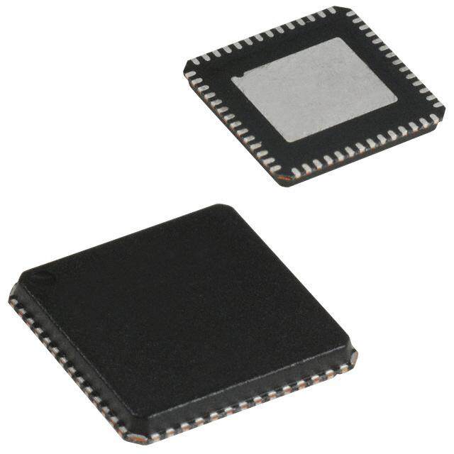
CYUSB301X/CYUSB201X Pin Configurations Figure 6. FX3 121-ball BGA Ball Map (Top View) 1 2 3 4 5 6 7 8 9 10 11 A U3VSSQ U3RXVDDQ SSRXM SSRXP SSTXP SSTXM AVDD VSS DP DM NC B VIO4 FSLC[0] R_USB3 FSLC[1] U3TXVDDQ CVDDQ AVSS VSS VSS VDD TRST# C GPIO[54] GPIO[55] VDD GPIO[57] RESET# XTALIN XTALOUT R_USB2 OTG_ID TDO VIO5 D GPIO[50] GPIO[51] GPIO[52] GPIO[53] GPIO[56] CLKIN_32 CLKIN VSS I2C_GPIO[58] I2C_GPIO[59] O[60] E GPIO[47] VSS VIO3 GPIO[49] GPIO[48] FSLC[2] TDI TMS VDD VBATT VBUS F VIO2 GPIO[45] GPIO[44] GPIO[41] GPIO[46] TCK GPIO[2] GPIO[5] GPIO[1] GPIO[0] VDD G VSS GPIO[42] GPIO[43] GPIO[30] GPIO[25] GPIO[22] GPIO[21] GPIO[15] GPIO[4] GPIO[3] VSS H VDD GPIO[39] GPIO[40] GPIO[31] GPIO[29] GPIO[26] GPIO[20] GPIO[24] GPIO[7] GPIO[6] VIO1 J GPIO[38] GPIO[36] GPIO[37] GPIO[34] GPIO[28] GPIO[16] GPIO[19] GPIO[14] GPIO[9] GPIO[8] VDD K GPIO[35] GPIO[33] VSS VSS GPIO[27] GPIO[23] GPIO[18] GPIO[17] GPIO[13] GPIO[12] GPIO[10] L VSS VSS VSS GPIO[32] VDD VSS VDD INT# VIO1 GPIO[11] VSS Note No ball is populated at location A9. Figure 7. FX3 Hi-Speed 121-Ball BGA Ball Map (Top View) 1 2 3 4 5 6 7 8 9 10 11 A U3VSSQ VDD NC NC NC NC AVDD VSS DP DM NC B VIO4 FSLC[0] NC FSLC[1] VDD CVDDQ AVSS VSS VSS VDD TRST# C GPIO[54] GPIO[55] VDD GPIO[57] RESET# XTALIN XTALOUT R_USB2 OTG_ID TDO VIO5 D GPIO[50] GPIO[51] GPIO[52] GPIO[53] GPIO[56] CLKIN_32 CLKIN VSS I2C_GPIO[58] I2C_GPIO[59] O[60] E GPIO[47] VSS VIO3 GPIO[49] GPIO[48] FSLC[2] TDI TMS VDD VBATT VBUS F VIO2 GPIO[45] GPIO[44] GPIO[41] GPIO[46] TCK GPIO[2] GPIO[5] GPIO[1] GPIO[0] VDD G VSS GPIO[42] GPIO[43] GPIO[30] GPIO[25] GPIO[22] GPIO[21] GPIO[15] GPIO[4] GPIO[3] VSS H VDD GPIO[39] GPIO[40] GPIO[31] GPIO[29] GPIO[26] GPIO[20] GPIO[24] GPIO[7] GPIO[6] VIO1 J GPIO[38] GPIO[36] GPIO[37] GPIO[34] GPIO[28] GPIO[16] GPIO[19] GPIO[14] GPIO[9] GPIO[8] VDD K GPIO[35] GPIO[33] VSS VSS GPIO[27] GPIO[23] GPIO[18] GPIO[17] GPIO[13] GPIO[12] GPIO[10] L VSS VSS VSS GPIO[32] VDD VSS VDD INT# VIO1 GPIO[11] VSS Document Number: 001-52136 Rev. *V Page 14 of 53
CYUSB301X/CYUSB201X Pin Description Table 7. CYUSB3012 and CYUSB3014 Pin List Power BGA I/O Name Description Domain GPIF II Interface Slave FIFO Interface F10 VIO1 I/O GPIO[0] DQ[0] DQ[0] F9 VIO1 I/O GPIO[1] DQ[1] DQ[1] F7 VIO1 I/O GPIO[2] DQ[2] DQ[2] G10 VIO1 I/O GPIO[3] DQ[3] DQ[3] G9 VIO1 I/O GPIO[4] DQ[4] DQ[4] F8 VIO1 I/O GPIO[5] DQ[5] DQ[5] H10 VIO1 I/O GPIO[6] DQ[6] DQ[6] H9 VIO1 I/O GPIO[7] DQ[7] DQ[7] J10 VIO1 I/O GPIO[8] DQ[8] DQ[8] J9 VIO1 I/O GPIO[9] DQ[9] DQ[9] K11 VIO1 I/O GPIO[10] DQ[10] DQ[10] L10 VIO1 I/O GPIO[11] DQ[11] DQ[11] K10 VIO1 I/O GPIO[12] DQ[12] DQ[12] K9 VIO1 I/O GPIO[13] DQ[13] DQ[13] J8 VIO1 I/O GPIO[14] DQ[14] DQ[14] G8 VIO1 I/O GPIO[15] DQ[15] DQ[15] J6 VIO1 I/O GPIO[16] PCLK CLK K8 VIO1 I/O GPIO[17] CTL[0] SLCS# K7 VIO1 I/O GPIO[18] CTL[1] SLWR# J7 VIO1 I/O GPIO[19] CTL[2] SLOE# H7 VIO1 I/O GPIO[20] CTL[3] SLRD# G7 VIO1 I/O GPIO[21] CTL[4] FLAGA G6 VIO1 I/O GPIO[22] CTL[5] FLAGB K6 VIO1 I/O GPIO[23] CTL[6] GPIO H8 VIO1 I/O GPIO[24] CTL[7] PKTEND# G5 VIO1 I/O GPIO[25] CTL[8] GPIO H6 VIO1 I/O GPIO[26] CTL[9] GPIO K5 VIO1 I/O GPIO[27] CTL[10] GPIO J5 VIO1 I/O GPIO[28] CTL[11] A1 H5 VIO1 I/O GPIO[29] CTL[12] A0 G4 VIO1 I/O GPIO[30] PMODE[0] PMODE[0] H4 VIO1 I/O GPIO[31] PMODE[1] PMODE[1] L4 VIO1 I/O GPIO[32] PMODE[2] PMODE[2] L8 VIO1 I/O INT# INT#/CTL[15] CTL[15] 32-bit Data 16 - bit Data Bus + 16 - bit Data 16 - bit Data 16 - bit Data GPIO Bus UART+SPI+I2S Bus + Bus + Bus + only UART+GPIO SPI+GPIO I2S+GPIO K2 VIO2 I/O GPIO[33] DQ[16] GPIO GPIO GPIO GPIO GPIO J4 VIO2 I/O GPIO[34] DQ[17] GPIO GPIO GPIO GPIO GPIO K1 VIO2 I/O GPIO[35] DQ[18] GPIO GPIO GPIO GPIO GPIO J2 VIO2 I/O GPIO[36] DQ[19] GPIO GPIO GPIO GPIO GPIO J3 VIO2 I/O GPIO[37] DQ[20] GPIO GPIO GPIO GPIO GPIO Document Number: 001-52136 Rev. *V Page 15 of 53
CYUSB301X/CYUSB201X Table 7. CYUSB3012 and CYUSB3014 Pin List (continued) Power BGA I/O Name Description Domain J1 VIO2 I/O GPIO[38] DQ[21] GPIO GPIO GPIO GPIO GPIO H2 VIO2 I/O GPIO[39] DQ[22] GPIO GPIO GPIO GPIO GPIO H3 VIO2 I/O GPIO[40] DQ[23] GPIO GPIO GPIO GPIO GPIO F4 VIO2 I/O GPIO[41] DQ[24] GPIO GPIO GPIO GPIO GPIO G2 VIO2 I/O GPIO[42] DQ[25] GPIO GPIO GPIO GPIO GPIO G3 VIO2 I/O GPIO[43] DQ[26] GPIO GPIO GPIO GPIO GPIO F3 VIO2 I/O GPIO[44] DQ[27] GPIO GPIO GPIO GPIO GPIO F2 VIO2 I/O GPIO[45] GPIO GPIO GPIO GPIO GPIO GPIO F5 VIO3 I/O GPIO[46] DQ[28] UART_RT S GPIO GPIO GPIO GPIO E1 VIO3 I/O GPIO[47] DQ[29] UART_CT S GPIO GPIO GPIO GPIO E5 VIO3 I/O GPIO[48] DQ[30] UART_TX GPIO GPIO GPIO GPIO E4 VIO3 I/O GPIO[49] DQ[31] UART_R X GPIO GPIO GPIO GPIO D1 VIO3 I/O GPIO[50] I2S_CLK I2S_CLK GPIO GPIO GPIO GPIO D2 VIO3 I/O GPIO[51] I2S_SD I2S_SD GPIO GPIO GPIO GPIO D3 VIO3 I/O GPIO[52] I2S_WS I2S_WS GPIO GPIO GPIO GPIO D4 VIO4 I/O GPIO[53] UART_RTS SPI_SCK UART_RTS SPI_SCK GPIO GPIO C1 VIO4 I/O GPIO[54] UART_CTS SPI_SSN UART_CTS SPI_SSN I2S_CLK GPIO C2 VIO4 I/O GPIO[55] UART_TX SPI_MIS O UART_TX SPI_MISO I2S_SD GPIO D5 VIO4 I/O GPIO[56] UART_RX SPI_MOS I UART_RX SPI_MOSI I2S_WS GPIO C4 VIO4 I/O GPIO[57] I2S_MCLK I2S_MCL K GPIO GPIO I2S_MCL K GPIO USB Port CYUSB301X CYUSB201X A3 U3RXVD DQ I SSRXM SSRX- NC A4 U3RXVD DQ I SSRXP SSRX+ NC A6 U3TXVD DQ O SSTXM SSTX- NC A5 U3TXVD DQ O SSTXP SSTX+ NC B3 U3TXVD DQ I/O R_usb3 Precision resistor for USB 3.0 (Connect a 200 NC ±1% resistor between this pin and GND) C9 VBUS/ VBATT I OTG_ID OTG_ID A9 VBUS/V BATT I/O DP D+ A10 VBUS/V BATT I/O DM D– C8 VBUS/VBATT I/O R_usb2 Precision resistor for USB 2.0 (Connect a 6.04 k ±1% resistor between this pin and GND) Clock and Reset B2 CVDDQ I FSLC[0] FSLC[0] C6 AVDD I/O XTALIN XTALIN C7 AVDD I/O XTALOUT XTALOUT B4 CVDDQ I FSLC[1] FSLC[1] E6 CVDDQ I FSLC[2] FSLC[2] D7 CVDDQ I CLKIN CLKIN D6 CVDDQ I CLKIN_32 CLKIN_32 C5 CVDDQ I RESET# RESET# I2C and JTAG D9 VIO5 I/O I2C_GPIO[58 I2C_SCL ] Document Number: 001-52136 Rev. *V Page 16 of 53
CYUSB301X/CYUSB201X Table 7. CYUSB3012 and CYUSB3014 Pin List (continued) Power BGA I/O Name Description Domain D10 VIO5 I/O I2C_GPIO[59 I2C_SDA ] E7 VIO5 I TDI TDI C10 VIO5 O TDO TDO B11 VIO5 I TRST# TRST# E8 VIO5 I TMS TMS F6 VIO5 I TCK TCK D11 VIO5 O O[60] Charger detect output Power E10 – PWR VBATT – B10 – PWR VDD – – – PWR VDD – A1 – PWR U3VSSQ – E11 – PWR VBUS – D8 – PWR VSS – H11 – PWR VIO1 – E2 – PWR VSS – L9 – PWR VIO1 – G1 – PWR VSS – – – PWR VIO1 – – – PWR VSS – F1 – PWR VIO2 – G11 – PWR VSS – – PWR VIO2 – E3 – PWR VIO3 – L1 – PWR VSS – B1 – PWR VIO4 – L6 – PWR VSS – – – PWR VSS – B6 – PWR CVDDQ – B5 – PWR U3TXVDDQ – A2 – PWR U3RXVDDQ – C11 – PWR VIO5 – L11 – PWR VSS – A7 – PWR AVDD – B7 – PWR AVSS – C3 – PWR VDD – B8 – PWR VSS – E9 – PWR VDD – B9 – PWR VSS – F11 – PWR VDD – – – PWR VSS GND – – PWR VDD – – – PWR VSS GND Document Number: 001-52136 Rev. *V Page 17 of 53
CYUSB301X/CYUSB201X Table 7. CYUSB3012 and CYUSB3014 Pin List (continued) Power BGA I/O Name Description Domain – – PWR VSS GND H1 – PWR VDD – L7 – PWR VDD – J11 – PWR VDD – L5 – PWR VDD – K4 – PWR VSS – L3 – PWR VSS – K3 – PWR VSS – L2 – PWR VSS – A8 – PWR VSS – – – – NC No Connect A11 – – NC No Connect Document Number: 001-52136 Rev. *V Page 18 of 53
CYUSB301X/CYUSB201X Electrical Specifications ■Additional ESD protection levels on D+, D–, and GND pins, and serial peripheral pins Absolute Maximum Ratings ■± 6-kV contact discharge, ± 8-kV air gap discharge based on Exceeding maximum ratings may shorten the useful life of the IEC61000-4-2 level 3A, ± 8-kV contact discharge, and ± 15-kV device. air gap discharge based on IEC61000-4-2 level 4C Storage temperature .................................... –65°C to +150°C Latch-up current .........................................................> 200mA Ambient temperature with Maximum output short-circuit current for all I/Os power supplied (Industrial) ............................ –40°C to +85°C (cumulative)..................................................................–100mA Ambient temperature with Maximum output current per I/O power supplied (Commercial) .............................0 °C to +70 °C (source or sink).......................... ......................................20mA Supply voltage to ground potential Operating Conditions V , A ......................................................................1.25V DD VDDQ T (ambient temperature under bias) V ,V , V , V , V ................................................3.6V A IO1 IO2 IO3 IO4 IO5 Industrial ........................................................ –40°C to +85°C U3TX , U3RX ...................................................1.25V VDDQ VDDQ Commercial ....................................................... 0 °C to +70 °C DC input voltage to any input pin ............................V + 0.3V CC V , A , U3TX , U3RX DC voltage applied to DD VDDQ VDDQ VDDQ outputs in high Z state ............................................V + 0.3V Supply voltage ..................................................1.15V to 1.25V CC (VCC is the corresponding I/O voltage) VBATT supply voltage ...............................................3.2V to 6V Static discharge voltage ESD protection levels: VIO1, VIO2, VIO3, VIO4, CVDDQ ■± 2.2-kV HBM based on JESD22-A114 Supply voltage ......................................................1.7V to 3.6V V supply voltage ............................................ 1.15V to 3.6V IO5 DC Specifications Table 8. DC Specifications Parameter Description Min Max Units Notes V Core voltage supply 1.15 1.25 V 1.2-V typical DD A Analog voltage supply 1.15 1.25 V 1.2-V typical VDD V GPIF II I/O power supply domain 1.7 3.6 V 1.8-, 2.5-, and 3.3-V typical IO1 V IO2 power supply domain 1.7 3.6 V 1.8-, 2.5-, and 3.3-V typical IO2 V IO3 power supply domain 1.7 3.6 V 1.8-, 2.5-, and 3.3-V typical IO3 V UART/SPI/I2S power supply domain 1.7 3.6 V 1.8-, 2.5-, and 3.3-V typical IO4 V USB voltage supply 3.2 6 V 3.7-V typical BATT V USB voltage supply 4.0 6 V 5-V typical BUS 1.2-V typical. A 22-µF bypass capacitor is U3TX USB3.0 1.2-V supply 1.15 1.25 V required on this power supply. VDDQ N/A for CYUSB201X 1.2-V typical. A 22-µF bypass capacitor is U3RX USB3.0 1.2-V supply 1.15 1.25 V required on this power supply. VDDQ N/A for CYUSB201X C Clock voltage supply 1.7 3.6 V 1.8-, 3.3-V typical VDDQ V I2C and JTAG voltage supply 1.15 3.6 V 1.2-, 1.8-, 2.5-, and 3.3-V typical IO5 0.625 × For 2.0V V 3.6V (except USB port). V Input HIGH voltage 1 VCC + 0.3 V CC IH1 VCC VCC is the corresponding I/O voltage supply. For 1.7V V 2.0V CC V Input HIGH voltage 2 VCC – 0.4 VCC + 0.3 V (except USB port). VCC is the corresponding IH2 I/O voltage supply. V Input LOW voltage –0.3 0.25 × VCC V VCC is the corresponding I/O voltage supply. IL Document Number: 001-52136 Rev. *V Page 19 of 53
CYUSB301X/CYUSB201X Table 8. DC Specifications (continued) Parameter Description Min Max Units Notes I (max) = –100µA tested at quarter drive OH V Output HIGH voltage 0.9 × VCC – V strength. VCC is the corresponding I/O OH voltage supply. I (min) = +100 µA tested at quarter drive OL V Output LOW voltage – 0.1 × VCC V strength. VCC is the corresponding I/O OL voltage supply. All I/O signals held at V Input leakage current for all pins DDQ (For I/Os with a pull-up or pull-down resistor I except –1 1 µA IX connected, the leakage current increases by SSTXP/SSXM/SSRXP/SSRXM V /R or V /R DDQ pu DDQ PD Output High-Z leakage current for all I pins except SSTXP/ SSXM/ –1 1 µA All I/O signals held at V OZ DDQ SSRXP/SSRXM Core and analog voltage operating I Core – 200 mA Total current through A , V CC current VDD DD I USB USB voltage supply operating current – 60 mA – CC Core current: 1.5 mA I/O current: 20 µA Total suspend current during USB current: 2 mA I suspend mode with USB 3.0 PHY – – mA SB1 For typical PVT (typical silicon, all power enabled (L1) supplies at their respective nominal levels at 25°C) Core current: 250 µA I/O current: 20 µA Total suspend current during USB current: 1.2 mA I suspend mode with USB 3.0 PHY – – mA SB2 For typical PVT (Typical silicon, all power disabled (L2) supplies at their respective nominal levels at 25°C) Core current: 60 µA I/O current: 20 µA Total standby current during standby USB current: 40 µA I – – µA SB3 mode (L3) For typical PVT (typical silicon, all power supplies at their respective nominal levels at 25°C) Core current: 0 µA I/O current: 20 µA Total standby current during core USB current: 40 µA I – – µA SB4 power-down mode (L4) For typical PVT (typical silicon, all power supplies at their respective nominal levels at 25°C) Voltage ramp rate on core and I/O V 0.2 50 V/ms Voltage ramp must be monotonic RAMP supplies Noise level permitted on V and I/O Max p-p noise level permitted on all supplies V DD – 100 mV N supplies except A VDD V Noise level permitted on A supply – 20 mV Max p-p noise level permitted on A N_AVDD VDD VDD Document Number: 001-52136 Rev. *V Page 20 of 53
CYUSB301X/CYUSB201X AC Timing Parameters GPIF II Timing Figure 8. GPIF II Timing in Synchronous Mode tCLKH tCLKL CLK tCLK tCO tHZ tCOE tDS tDH tLZ tLZ tDOH tDOH Data1 Data2 DQ- [31:0] Data( IN) (OUT) (OUT) tS tH CTL(IN) tCTLO tCOH CTL (OUT) Table 9. GPIF II Timing Parameters in Synchronous Mode [2] Parameter Description Min Max Units Frequency Interface clock frequency – 100 MHz tCLK Interface clock period 10 – ns tCLKH Clock high time 4 – ns tCLKL Clock low time 4 – ns tS CTL input to clock setup time 2 – ns tH CTL input to clock hold time 0.5 – ns tDS Data in to clock setup time 2 – ns tDH Data in to clock hold time 0.5 – ns tCO Clock to data out propagation delay when DQ bus is already in output direction – 7 ns Clock to data out propagation delay when DQ lines change to output from tristate tCOE – 9 ns and valid data is available on the DQ bus tCTLO Clock to CTL out propagation delay – 8 ns tDOH Clock to data out hold 2 – ns tCOH Clock to CTL out hold 0 – ns tHZ Clock to high-Z – 8 ns tLZ Clock to low-Z 0 – ns Note 2. All parameters guaranteed by design and validated through characterization. Document Number: 001-52136 Rev. *V Page 21 of 53
CYUSB301X/CYUSB201X Figure 9. GPIF II Timing in Asynchronous Mode tDS/ tAS tDH/tAH DATA/ ADDR DATA IN tCHZ tCTLassert_DQlatch CTL# tCTLdeassert_DQlatch (I/P, ALE/DLE) tAA/tDO tCHZ/tOEHZ tCLZ/tOELZ DATA OUT DATA OUT CTL# tCTLassert tCTLdeassert (I/P, non ALE/ DLE tCTLalpha ALPHA O/P tCTLbeta BETA O/P tCTLassert 1 tCTLdeassert 1 tCTL# (O/P) 1. n is an integer >= 0 tDST tDHT DATA/ ADDR tCTLdeassert_DQassert CTL# tCTLassert_DQassert I/P (non DLE/ALE) Figure 10. GPIF II Timing in Asynchronous DDR Mode tDS tCTLdeassert_DqlatchDDR tCTLassert_DQlatchDDR CTL# (I/P) tDS tDH tDH DATA IN Document Number: 001-52136 Rev. *V Page 22 of 53
CYUSB301X/CYUSB201X Table 10. GPIF II Timing in Asynchronous Mode[3, 4] Note The following parameters assume one state transition Parameter Description Min Max Units tDS Data In to DLE setup time. Valid in DDR async mode. 2.3 – ns tDH Data In to DLE hold time. Valid in DDR async mode. 2 – ns tAS Address In to ALE setup time 2.3 – ns tAH Address In to ALE hold time 2 – ns CTL I/O asserted width for CTRL inputs without DQ input association tCTLassert 7 – ns and for outputs. CTL I/O deasserted width for CTRL inputs without DQ input associ- tCTLdeassert 7 – ns ation and for outputs. CTL asserted pulse width for CTL inputs that signify DQ inputs valid tCTLassert_DQassert at the asserting edge but do not employ in-built latches (ALE/DLE) for 20 – ns those DQ inputs. CTL deasserted pulse width for CTL inputs that signify DQ input valid tCTLdeassert_DQassert at the asserting edge but do not employ in-built latches (ALE/DLE) for 7 – ns those DQ inputs. CTL asserted pulse width for CTL inputs that signify DQ inputs valid tCTLassert_DQdeassert at the deasserting edge but do not employ in-built latches (ALE/DLE) 7 – ns for those DQ inputs. CTL deasserted pulse width for CTL inputs that signify DQ inputs valid tCTLdeassert_DQdeassert at the deasserting edge but do not employ in-built latches (ALE/DLE) 20 – ns for those DQ inputs. CTL asserted pulse width for CTL inputs that employ in-built latches tCTLassert_DQlatch (ALE/DLE) to latch the DQ inputs. In this non-DDR case, in-built 7 – ns latches are always close at the deasserting edge. CTL deasserted pulse width for CTL inputs that employ in-built latches tCTLdeassert_DQlatch (ALE/DLE) to latch the DQ inputs. In this non-DDR case, in-built 10 – ns latches always close at the deasserting edge. CTL asserted pulse width for CTL inputs that employ in-built latches tCTLassert_DQlatchDDR 10 – ns (DLE) to latch the DQ inputs in DDR mode. CTL deasserted pulse width for CTL inputs that employ in-built latches tCTLdeassert_DQlatchDDR 10 – ns (DLE) to latch the DQ inputs in DDR mode. DQ/CTL input to DQ output time when DQ change or CTL change tAA needs to be detected and affects internal updates of input and output – 30 ns DQ lines. CTL to data out when the CTL change merely enables the output flop tDO – 25 ns update whose data was already established. CTL designated as OE to low-Z. Time when external devices should tOELZ 0 – ns stop driving data. tOEHZ CTL designated as OE to high-Z 8 8 ns CTL (non-OE) to low-Z. Time when external devices should stop tCLZ 0 – ns driving data. tCHZ CTL (non-OE) to high-Z 30 30 ns tCTLalpha CTL to alpha change at output – 25 ns tCTLbeta CTL to beta change at output – 30 ns tDST Addr/data setup when DLE/ALE not used 2 – ns tDHT Addr/data hold when DLE/ALE not used 20 – ns Notes 3. All parameters guaranteed by design and validated through characterization. 4. "alpha" output corresponds to "early output" and "beta" corresponds to "delayed output". Please refer to the GPIFII Designer Tool for the use of these outputs. Document Number: 001-52136 Rev. *V Page 23 of 53
CYUSB301X/CYUSB201X Slave FIFO Interface FLAG Usage: The FLAG signals are monitored for flow control by the external Synchronous Slave FIFO Read Sequence Description processor. FLAG signals are outputs from FX3 that may be ■FIFO address is stable and SLCS is asserted configured to show empty, full, or partial status for a dedicated thread or the current thread that is addressed. ■FLAG indicates FIFO not empty status Socket Switching Delay (Tssd): ■SLOE is asserted. SLOE is an output-enable only, whose sole The socket-switching delay is measured from the time function is to drive the data bus. EPSWITCH# is asserted by the master, with the new socket ■SLRD is asserted address on the address bus, to the time the Current_Thread_D- MA_Ready flag is asserted. For the Producer socket, the flag is The FIFO pointer is updated on the rising edge of the PCLK, asserted when it is ready to receive data in the DMA buffer. For while the SLRD is asserted. This starts the propagation of data the Consumer socket, the flag is asserted when it is ready to from the newly addressed location to the data bus. After a propa- drive data out of the DMA buffer. For a synchronous slave FIFO gation delay of tco (measured from the rising edge of PCLK), the interface, the switching delay is measured in the number of GPIF new data value is present. N is the first data value read from the interface clock cycles; for an asynchronous slave FIFO interface, FIFO. To have data on the FIFO data bus, SLOE must also be in PIB clock cycles. This is applicable only for the 5-bit Slave asserted. FIFO interface; there is no socket-switching delay in FX3's 2-bit The same sequence of events is applicable for a burst read. Slave FIFO interface, which makes use of thread switching in the GPIF™ II state machine. Note For burst mode, the SLRD# and SLOE# are asserted during the entire duration of the read. When SLOE# is asserted, the data bus is driven (with data from the previously addressed FIFO). For each subsequent rising edge of PCLK, while the SLRD# is asserted, the FIFO pointer is incremented and the next data value is placed on the data bus. Figure 11. Synchronous Slave FIFO Read Mode Synchronous Read Cycle Timing tCYC PCLK tCH tCL tACCD SLCS tAStAH FIFO ADDR An Am tRDStRDH SLRD SLOE Tssd tACCD tCFLG Tssd FLAGA (dedicated thread Flag for An) (1 = Not Empty 0= Empty) tCFLG FLAGB (dedicated thread Flag for Am) (1 = Not Empty 0= Empty) tOELZ tOEZ tCDH tCO t OEZ Data Out High-Z drDivaetna :DN(An) High-Z DN (An) DN(Am) DN+1 (Am) DN+2 (Am) High-Z SLWR( HIGH) Document Number: 001-52136 Rev. *V Page 24 of 53
CYUSB301X/CYUSB201X Synchronous Slave FIFO Write Sequence Description Short Packet: A short packet can be committed to the USB host by using the PKTEND#. The external device or processor should ■FIFO address is stable and the signal SLCS# is asserted be designed to assert the PKTEND# along with the last word of ■External master or peripheral outputs the data to the data bus data and SLWR# pulse corresponding to the last word. The ■SLWR# is asserted FIFOADDR lines must be held constant during the PKTEND# assertion. ■While the SLWR# is asserted, data is written to the FIFO and on the rising edge of the PCLK, the FIFO pointer is incremented Zero-Length Packet: The external device or processor can signal a Zero-Length Packet (ZLP) to FX3 simply by asserting ■The FIFO flag is updated after a delay of t from the rising WFLG PKTEND#, without asserting SLWR#. SLCS# and address must edge of the clock be driven as shown in Figure12. The same sequence of events is also applicable for burst write Note For the burst mode, SLWR# and SLCS# are asserted for the entire duration, during which all the required data values are written. In this burst write mode, after the SLWR# is asserted, the data on the FIFO data bus is written to the FIFO on every rising edge of PCLK. The FIFO pointer is updated on each rising edge of PCLK. Figure 12. Synchronous Slave FIFO Write Mode Synchronous Write Cycle Timing tCYC PCLK tCH tCL SLCS tAS tAH FIFO ADDR An Am Tssd tWRS tWRH SLWR tFAD tCFLG FLAGA dedicated thread FLAG for An (1 = Not Full0 = Full) Tssd tFAD tCFLG FLAGB current thread FLAG for Am (1 = Not Full0 = Full) tDS tDH tDS tDH tDH Data IN High-Z DN(An) DN(Am) DN+1(Am) DN+2(Am) tPEStPEH PKTEND SLOE (HIGH) Document Number: 001-52136 Rev. *V Page 25 of 53
CYUSB301X/CYUSB201X Figure 13. Synchronous Slave FIFO ZLP Write Cycle Timing Synchronous ZLP Write Cycle Timing tCYC PCLK tCH tCL SLCS tAS tAH FIFO ADDR An SLWR (HIGH) tPEStPEH PKTEND FLAGA tCFLG dedicated thread FLAG for An (1 = Not Full 0= Full) FLAGB current thread FLAG for Am (1 = Not Full 0= Full) Data IN High-Z SLOE (HIGH) Table 11. Synchronous Slave FIFO Parameters[5] Parameter Description Min Max Units FREQ Interface clock frequency – 100 MHz tCYC Clock period 10 – ns tCH Clock high time 4 – ns tCL Clock low time 4 – ns tRDS SLRD# to CLK setup time 2 – ns tRDH SLRD# to CLK hold time 0.5 – ns tWRS SLWR# to CLK setup time 2 – ns tWRH SLWR# to CLK hold time 0.5 – ns tCO Clock to valid data – 7 ns tDS Data input setup time 2 – ns tDH CLK to data input hold 0.5 – ns tAS Address to CLK setup time 2 – ns tAH CLK to address hold time 0.5 – ns tOELZ SLOE# to data low-Z 0 – ns tCFLG CLK to flag output propagation delay – 8 ns tOEZ SLOE# deassert to Data Hi Z – 8 ns tPES PKTEND# to CLK setup 2 – ns tPEH CLK to PKTEND# hold 0.5 – ns tCDH CLK to data output hold 2 – ns tSSD Socket switching delay 2 68 Clock cycles tACCD Latency from SLRD# to Data 2 2 Clock cycles tFAD Latency from SLWR# to FLAG 3 3 Clock cycles Note Three-cycle latency from ADDR to DATA/FLAGS. Note 5. All parameters guaranteed by design and validated through characterization. Document Number: 001-52136 Rev. *V Page 26 of 53
CYUSB301X/CYUSB201X Asynchronous Slave FIFO Read Sequence Description In Figure 14, data N is the first valid data read from the FIFO. For data to appear on the data bus during the read cycle, SLOE# ■FIFO address is stable and the SLCS# signal is asserted. must be in an asserted state. SLRD# and SLOE# can also be ■SLOE# is asserted. This results in driving the data bus. tied. The same sequence of events is also shown for a burst read. ■SLRD # is asserted. Note In the burst read mode, during SLOE# assertion, the data ■Data from the FIFO is driven after assertion of SLRD#. This bus is in a driven state (data is driven from a previously data is valid after a propagation delay of tRDO from the falling addressed FIFO). After assertion of SLRD# data from the FIFO edge of SLRD#. is driven on the data bus (SLOE# must also be asserted). The ■FIFO pointer is incremented on deassertion of SLRD# FIFO pointer is incremented after deassertion of SLRD#. Figure 14. Asynchronous Slave FIFO Read Mode Asynchronous Read Cycle Timing SLCS tAS tAH FIFO ADDR An Am t t RDl RDh SLRD SLOE tFLG tRFLG FLAGA dedicated thread Flag for An (1=Not empty 0 = Empty) FLAGB dedicated thread Flag for Am (1=Not empty 0 = Empty) tOE tRDO tOH tOE tRDO tRDO tOH t LZ Data Out High-Z DN(An) DN(An) DN(Am) DN+1(Am) DN+2(Am) SLWR (HIGH) Document Number: 001-52136 Rev. *V Page 27 of 53
CYUSB301X/CYUSB201X Asynchronous Slave FIFO Write Sequence Description Short Packet: A short packet can be committed to the USB host by using the PKTEND#. The external device or processor should ■FIFO address is driven and SLCS# is asserted be designed to assert the PKTEND# along with the last word of ■SLWR# is asserted. SLCS# must be asserted with SLWR# or data and SLWR# pulse corresponding to the last word. The before SLWR# is asserted FIFOADDR lines must be held constant during the PKTEND# assertion. ■Data must be present on the tWRS bus before the deasserting Zero-Length Packet: The external device or processor can edge of SLWR# signal a zero-length packet (ZLP) to FX3 simply by asserting ■Deassertion of SLWR# causes the data to be written from the PKTEND#, without asserting SLWR#. SLCS# and the address data bus to the FIFO, and then the FIFO pointer is incremented must be driven as shown in Figure 16 on page 29. ■The FIFO flag is updated after the tWFLG from the deasserting FLAG Usage: The FLAG signals are monitored by the external edge of SLWR. processor for flow control. FLAG signals are FX3 outputs that can be configured to show empty, full, and partial status for a The same sequence of events is shown for a burst write. dedicated address or the current address. Note that in the burst write mode, after SLWR# deassertion, the data is written to the FIFO, and then the FIFO pointer is incre- mented. Figure 15. Asynchronous Slave FIFO Write Mode Asynchronous Write Cycle Timing SLCS tAS tAH FIFO ADDR An Am tWRl tWRh SLWR t FLG t WFLG F LAGA dedicated thread Flag for An t WFLG (1=Not Full 0 = Full) (1=deNdoicta Fteudll 0 t h = Fr Fe LauAldlG) FBlag for Am StWR tWRH StWR tWRH DATA In High-Z DN(An) DN(Am) DN+1(Am) DN+2(Am) t WRPtE PEh PKTEND SLOE (HIGH) tWRPE: SLWR# de- assert to PKTEND deasser=t 2ns min( This means that PKTEND should not be be deasserted before SL#W)R Note: PKTEND must be asserted at the same time as SL#W.R Document Number: 001-52136 Rev. *V Page 28 of 53
CYUSB301X/CYUSB201X Figure 16. Asynchronous ZLP Write Cycle Timing SLCS tAS tAH FIFO ADDR An SLWR (HIGH) tPEl tPEh PKTEND t WFLG F LAGA dedicated thread Flag for An (1= Not Full 0 = Full) F LAGB dedicated thread Flag for Am (1= Not Full 0 = Full) DATA In High-Z SLOE (HIGH) Table 12. Asynchronous Slave FIFO Parameters[6] Parameter Description Min Max Units tRDI SLRD# low 20 – ns tRDh SLRD# high 10 – ns tAS Address to SLRD#/SLWR# setup time 7 – ns tAH SLRD#/SLWR#/PKTEND to address hold time 2 – ns tRFLG SLRD# to FLAGS output propagation delay – 35 ns tFLG ADDR to FLAGS output propagation delay – 22.5 ns tRDO SLRD# to data valid – 25 ns tOE OE# low to data valid – 25 ns tLZ OE# low to data low-Z 0 – ns tOH SLOE# deassert data output hold – 22.5 ns tWRI SLWR# low 20 – ns tWRh SLWR# high 10 – ns tWRS Data to SLWR# setup time 7 – ns tWRH SLWR# to Data Hold time 2 – ns tWFLG SLWR#/PKTEND to Flags output propagation delay – 35 ns tPEI PKTEND low 20 – ns tPEh PKTEND high 7.5 – ns tWRPE SLWR# deassert to PKTEND deassert 2 – ns Note 6. All parameters guaranteed by design and validated through characterization. Document Number: 001-52136 Rev. *V Page 29 of 53
CYUSB301X/CYUSB201X Host Processor Interface (P-Port) Timing Asynchronous SRAM Timing Figure 17. Non-multiplexed Asynchronous SRAM Read Timing Socket Read – Address Transition Controlled Timing (OE# is asserted) A[0] tAA tOH tAH HIGH DATA IMPEDANCE OUT DATA VALID DATA VALID DATA VALID OE# tOE OE# Controlled Timing ADDRESS WE# (HIGH) tAOS CE# tOHC tRC OE# tOHH tOE tOLZ tOEZ HIGH HIGH HIGH IMPEDANCE IMPEDANCE DATA OUT IMPEDANCE DATA DATA VALID VALID Document Number: 001-52136 Rev. *V Page 30 of 53
CYUSB301X/CYUSB201X Figure 18. Non-multiplexed Asynchronous SRAM Write Timing (WE# and CE# Controlled) Write Cycle 1 WE# Controlled, OE# High During Write tWC ADDRESS tCW CE# tAW tAH tWP WE# tAS tWPH OE# tDS tDH DATA I/O VALID DATA VALID DATA tWHZ Write Cycle 2 CE# Controlled, OE# High During Write tWC ADDRESS tAS tCW tCPH CE# tAW tAH tWP WE# OE# tDS tDH DATA I/O VALID DATA VALID DATA tWHZ Document Number: 001-52136 Rev. *V Page 31 of 53
CYUSB301X/CYUSB201X Figure 19. Non-multiplexed Asynchronous SRAM Write Timing (WE# controlled, OE# LOW) Write Cycle 3 WE# Controlled. OE# Low tWC tCW CE# tAW tAH tAS tWP WE# tDS tDH DATA I/O VALID DATA tOW tWHZ Note: tWP must be adjusted such that tWP > tWHZ + tDS Table 13. Asynchronous SRAM Timing Parameters[7] Parameter Description Min Max Units – SRAM interface bandwidth – 61.5 Mbps tRC Read cycle time 32.5 – ns tAA Address to data valid – 30 ns tAOS Address to OE# LOW setup time 7 – ns tOH Data output hold from address change 3 – ns tOHH OE# HIGH hold time 7.5 – ns tOHC OE# HIGH to CE# HIGH 2 – ns tOE OE# LOW to data valid – 25 ns tOLZ OE# LOW to LOW-Z 0 – ns tWC Write cycle time 30 – ns tCW CE# LOW to write end 30 – ns tAW Address valid to write end 30 – ns tAS Address setup to write start 7 – ns tAH Address hold time from CE# or WE# 2 – ns tWP WE# pulse width 20 – ns tWPH WE# HIGH time 10 – ns tCPH CE# HIGH time 10 – ns tDS Data setup to write end 7 – ns tDH Data hold to write end 2 – ns tWHZ Write to DQ HIGH-Z output – 22.5 ns tOEZ OE# HIGH to DQ HIGH-Z output – 22.5 ns tOW End of write to LOW-Z output 0 – ns Note 7. All parameters guaranteed by design and validated through characterization. Document Number: 001-52136 Rev. *V Page 32 of 53
CYUSB301X/CYUSB201X ADMux Timing for Asynchronous Access Figure 20. ADMux Asynchronous Random Read tRC tACC Valid A[0:7]/DQ[0:15] Valid Address Valid Data Addr tAVS tAVH ADV# tVP WE# (HIGH) tCEAV tHZ tCO CE# tCPH tHZ tOLZ OE# tOE tAVOE Note: 1. Multiple read cycles can be executed while keeping CE# low. 2. Read operation ends with either de-assertion of either OE# or CE#, whichever comes earlier. Figure 21. ADMux Asynchronous Random Write tWC Valid A[0:7]/DQ[0:15] Address Valid Data Valid Addr tAW tAVS tAVH tDS tDH ADV# tVP tVPH tCEAV CE# tCPH tCW WE# tWP tWPH tAVWE Note: 1. Multiple write cycles can be executed while keeping CE# low. 2. Write operation ends with de-assertion of either WE# or CE#, whichever comes earlier. Document Number: 001-52136 Rev. *V Page 33 of 53
CYUSB301X/CYUSB201X Table 14. Asynchronous ADMux Timing Parameters[8] Parameter Description Min Max Units Notes ADMux Asynchronous READ Access Timing Parameters Read cycle time (address valid to address This parameter is dependent on when tRC 54.5 – ns valid) the P-port processors deasserts OE# tACC Address valid to data valid – 32 ns – tCO CE# assert to data valid – 34.5 ns – tAVOE ADV# deassert to OE# assert 2 – ns – tOLZ OE# assert to data LOW-Z 0 – ns – tOE OE# assert to data valid – 25 ns – tHZ Read cycle end to data HIGH-Z – 22.5 ns – ADMux Asynchronous WRITE Access Timing Parameters Write cycle time (Address Valid to Address tWC – 52.5 ns – Valid) tAW Address valid to write end 30 – ns – tCW CE# assert to write end 30 – ns – tAVWE ADV# deassert to WE# assert 2 – ns – tWP WE# LOW pulse width 20 – ns – tWPH WE# HIGH pulse width 10 – ns – tDS Data valid setup to WE# deassert 18 – ns – tDH Data valid hold from WE# deassert 2 – ns – ADMux Asynchronous Common READ/WRITE Access Timing Parameters tAVS Address valid setup to ADV# deassert 5 – ns – tAVH Address valid hold from ADV# deassert 2 – ns – tVP ADV# LOW pulse width 7.5 – ns – tCPH CE# HIGH pulse width 10 – ns – tVPH ADV# HIGH pulse width 15 – ns – tCEAV CE# assert to ADV# assert 0 – ns – Note 8. All parameters guaranteed by design and validated through characterization. Document Number: 001-52136 Rev. *V Page 34 of 53
CYUSB301X/CYUSB201X Synchronous ADMux Timing Figure 22. Synchronous ADMux Interface – Read Cycle Timing 2- cycle latency from OE# to DATA tCLK tCLKH tCLKL CLK tCO tS tH A[0:7]/DQ[0:31] Valid Address Valid Data tS tH ADV# tOHZ tS CE# tAVOE tOLZ OE# tKW tKW RDY tCH WE# (HIGH) Note: 1) External P-Port processor and FX3 operate on the same clock edge 2) External processor sees RDY assert 2 cycles after OE # asserts andand sees RDY deassert a cycle after the data appears on the output 3) Valid output data appears 2 cycle after OE # asserted. The data is held until OE # deasserts 4) Two cycle latency is shown for 0-100 MHz operation. Latency can be reduced by 1 cycle for operations at less than 50 MHz (this 1 cycle latency is not supported by the bootloader) Figure 23. Synchronous ADMux Interface – Write Cycle Timing 2-cycle latency between WE# and data being latched 2-cycle latency between this clk edge and RDY deassertion seen by the host CLK tCLK tS tH tDS tDH A[0:7]/DQ[0:31] Valid Address Valid Data tS tH ADV# tS CE# tAVWE tS tH WE# tKW RDY tKW Note: 1) External P-Port processor and FX3 operate on the same clock edge 2) External processor sees RDY assert 2 cycles after WE # asserts and deassert 3 cycles after the edge sampling the data. 3) Two cycle latency is shown for 0-100 MHz operation. Latency can be reduced by 1 cycle for operations at less than 50 MHz (this 1 cycle latency is not supported by the bootloader) Document Number: 001-52136 Rev. *V Page 35 of 53
CYUSB301X/CYUSB201X Figure 24. Synchronous ADMux Interface – Burst Read Timing 2-cycle latency from OE# to Data tCLK tCLKH tCLKL CLK tCO tS tH tCH A[0:7]/DQ[0:31] Valid Address D0 D1 D2 D3 tS tH ADV# tHZ tS CE# tAVOE tOLZ OE# tKW RDY tKW Note: 1) External P-Port processor and FX3 work operate on the same clock edge 2) External processor sees RDY assert 2 cycles after OE # asserts andand sees RDY deassert a cycle after the last burst data appears on the output 3) Valid output data appears 2 cycle after OE # asserted. The last burst data is held until OE # deasserts 4) Burst size of 4 is shown. Transfer size for the operation must be a multiple of burst size. Burst size is usually power of 2. RDY will not deassert in the middle of the burst. 5) External processor cannot deassert OE in the middle of a burst. If it does so, any bytes remaining in the burst packet could get lost. 6) Two cycle latency is shown for 0-100 MHz operation. Latency can be reduced by 1 cycle for operations at less than 50 MHz (this 1 cycle latency is not supported by the bootloader) Figure 25. Sync ADMux Interface – Burst Write Timing 2-cycle latency between WE# and data being latched 2-cycle latency between this clk edge and RDY deassertion seen by the host tCLKH tCLKL CLK tCLK tS tH tDS tDH tDH A[0:7]/DQ[0:31] Valid Address D0 D1 D2 D3 tS tH ADV# tS CE# tAVWE WE# tKW RDY tKW Note: 1) External P-Port processor and FX3 operate on the same clock edge 2) External processor sees RDY assert 2 cycles after WE # asserts and deasserts 3 cycles after the edge sampling the last burst data. 3) Transfer size for the operation must be a multiple of burst size. Burst size is usually power of 2. RDY will not deassert in the middle of the burst. Burst size of 4 is shown 4) External processor cannot deassert WE in the middle of a burst. If it does so, any bytes remaining in the burst packet could get lost. 5)Two cycle latency is shown for 0-100 MHz operation. Latency can be reduced by 1 cycle for operations at less than 50 MHz (this 1 cycle latency is not supported by the bootloader) Document Number: 001-52136 Rev. *V Page 36 of 53
CYUSB301X/CYUSB201X Table 15. Synchronous ADMux Timing Parameters[9] Parameter Description Min Max Unit FREQ Interface clock frequency – 100 MHz tCLK Clock period 10 – ns tCLKH Clock HIGH time 4 – ns tCLKL Clock LOW time 4 – ns tS CE#/WE#/DQ setup time 2 – ns tH CE#/WE#/DQ hold time 0.5 – ns tCH Clock to data output hold time 0 – ns tDS Data input setup time 2 – ns tDH Clock to data input hold 0.5 – ns tAVDOE ADV# HIGH to OE# LOW 0 – ns tAVDWE ADV# HIGH to WE# LOW 0 – ns tHZ CE# HIGH to Data HIGH-Z – 8 ns tOHZ OE# HIGH to Data HIGH-Z – 8 ns tOLZ OE# LOW to Data LOW-Z 0 – ns tKW Clock to RDY valid – 8 ns Serial Peripherals Timing I2C Timing Figure 26. I2C Timing Definition Note 9. All parameters guaranteed by design and validated through characterization. Document Number: 001-52136 Rev. *V Page 37 of 53
CYUSB301X/CYUSB201X Table 16. I2C Timing Parameters[10] Parameter Description Min Max Units I2C Standard Mode Parameters fSCL SCL clock frequency 0 100 kHz tHD:STA Hold time START condition 4 – µs tLOW LOW period of the SCL 4.7 – µs tHIGH HIGH period of the SCL 4 – µs tSU:STA Setup time for a repeated START condition 4.7 – µs tHD:DAT Data hold time 0 – µs tSU:DAT Data setup time 250 – ns tr Rise time of both SDA and SCL signals – 1000 ns tf Fall time of both SDA and SCL signals – 300 ns tSU:STO Setup time for STOP condition 4 – µs tBUF Bus free time between a STOP and START condition 4.7 – µs tVD:DAT Data valid time – 3.45 µs tVD:ACK Data valid ACK – 3.45 µs tSP Pulse width of spikes that must be suppressed by input filter n/a n/a I2C Fast Mode Parameters fSCL SCL clock frequency 0 400 kHz tHD:STA Hold time START condition 0.6 – µs tLOW LOW period of the SCL 1.3 – µs tHIGH HIGH period of the SCL 0.6 – µs tSU:STA Setup time for a repeated START condition 0.6 – µs tHD:DAT Data hold time 0 – µs tSU:DAT Data setup time 100 – ns tr Rise time of both SDA and SCL signals – 300 ns tf Fall time of both SDA and SCL signals – 300 ns tSU:STO Setup time for STOP condition 0.6 – µs tBUF Bus free time between a STOP and START condition 1.3 – µs tVD:DAT Data valid time – 0.9 µs tVD:ACK Data valid ACK – 0.9 µs tSP Pulse width of spikes that must be suppressed by input filter 0 50 ns Note 10.All parameters guaranteed by design and validated through characterization. Document Number: 001-52136 Rev. *V Page 38 of 53
CYUSB301X/CYUSB201X Table 16. I2C Timing Parameters[10] (continued) Parameter Description Min Max Units I2C Fast Mode Plus Parameters (Not supported at I2C_VDDQ=1.2V) fSCL SCL clock frequency 0 1000 kHz tHD:STA Hold time START condition 0.26 – µs tLOW LOW period of the SCL 0.5 – µs tHIGH HIGH period of the SCL 0.26 – µs tSU:STA Setup time for a repeated START condition 0.26 – µs tHD:DAT Data hold time 0 – µs tSU:DAT Data setup time 50 – ns tr Rise time of both SDA and SCL signals – 120 ns tf Fall time of both SDA and SCL signals – 120 ns tSU:STO Setup time for STOP condition 0.26 – µs tBUF Bus-free time between a STOP and START condition 0.5 – µs tVD:DAT Data valid time – 0.45 µs tVD:ACK Data valid ACK – 0.55 µs tSP Pulse width of spikes that must be suppressed by input filter 0 50 ns I2S Timing Diagram Figure 27. I2S Transmit Cycle t T t t TR TF tTL tTH SCK t Thd SA, WS (output) t Td Table 17. I2S Timing Parameters[11] Parameter Description Min Max Units tT I2S transmitter clock cycle Ttr – ns tTL I2S transmitter cycle LOW period 0.35 Ttr – ns tTH I2S transmitter cycle HIGH period 0.35 Ttr – ns tTR I2S transmitter rise time – 0.15 Ttr ns tTF I2S transmitter fall time – 0.15 Ttr ns tThd I2S transmitter data hold time 0 – ns tTd I2S transmitter delay time – 0.8tT ns Note tT is selectable through clock gears. Max Ttr is designed for 96-kHz codec at 32 bits to be 326 ns (3.072 MHz). Note 11.All parameters guaranteed by design and validated through characterization. Document Number: 001-52136 Rev. *V Page 39 of 53
CYUSB301X/CYUSB201X SPI Timing Specification Figure 28. SPI Timing SSN (output) t ssnh t sck t SCK tlead t lag (CPOL=0, rf Output) t t wsck wsck SCK (CPOL=1, Output) t sdi t hoi MISO (input) LSB MSB t t d t tdis sdd v di MOSI LSB MSB (output) SPI Master Timing for CPHA = 0 SSN (output) t ssnh t sck t t t lag SCK lead rf (CPOL=0, Output) t t wsck wsck SCK (CPOL=1, Output) tsdi thoi MISO LSB MSB (input) tdv tdi tdis MOSI LSB MSB (output) SPI Master Timing for CPHA = 1 Document Number: 001-52136 Rev. *V Page 40 of 53
CYUSB301X/CYUSB201X Table 18. SPI Timing Parameters[12] Parameter Description Min Max Units fop Operating frequency 0 33 MHz tsck Cycle time 30 – ns twsck Clock high/low time 13.5 – ns tlead SSN-SCK lead time 1/2 tsck[13]-5 1.5tsck[13]+ 5 ns tlag Enable lag time 0.5 1.5tsck[13]+5 ns trf Rise/fall time – 8 ns tsdd Output SSN to valid data delay time – 5 ns tdv Output data valid time – 5 ns tdi Output data invalid 0 – ns tssnh Minimum SSN high time 10 – ns tsdi Data setup time input 8 – ns thoi Data hold time input 0 – ns tdis Disable data output on SSN high 0 – ns Notes 12.All parameters guaranteed by design and validated through characterization. 13.Depends on LAG and LEAD setting in the SPI_CONFIG register. Document Number: 001-52136 Rev. *V Page 41 of 53
CYUSB301X/CYUSB201X Reset Sequence FX3’s hard reset sequence requirements are specified in this section. Table 19. Reset and Standby Timing Parameters Parameter Definition Conditions Min (ms) Max (ms) Clock Input 1 – tRPW Minimum RESET# pulse width Crystal Input 1 – tRH Minimum high on RESET# – 5 – Clock Input 1 – tRR Reset recovery time (after which Boot loader begins firmware download) Crystal Input 5 Time to enter standby/suspend (from the time MAIN_CLOCK_EN/ tSBY – – 1 MAIN_POWER_EN bit is set) Clock Input 1 – tWU Time to wakeup from standby Crystal Input 5 – tWH Minimum time before Standby/Suspend source may be reasserted – 5 – Figure 29. Reset Sequence VDD ( core) xVDDQ XTALIN/ CLKIN XTALIN/ CLKIN must be stable before exiting Standby/Suspend Mandatory tRR tRh Reset Pulse Hard Reset RESET # tRPW tWH Standby/ tSBY tWU Suspend Source Standby/Suspend source Is asserted Standby/Suspend (MAIN_POWER_EN/ MAIN_CLK_EN bit source Is deasserted is set) Document Number: 001-52136 Rev. *V Page 42 of 53
CYUSB301X/CYUSB201X Package Diagram Figure 30. 121-ball BGA Package Diagram 2X 0.10C E1 E B A (datum B) A1 CORNER 11 10 9 8 7 6 5 4 3 2 1 7 A1 CORNER A B C 6 D SD E D1 D F G (datum A) H J K eD L 0.10C 2X 6 TOP VIEW SE eE BOTTOM VIEW 0.20C DETAIL A A1 0.08C C 121XØb 5 A Ø0.15MCAB Ø0.08MC DETAIL A SIDE VIEW NOTES: DIMENSIONS 1. ALL DIMENSIONS ARE IN MILLIMETERS. SYMBOL MIN. NOM. MAX. 2. SOLDER BALL POSITION DESIGNATION PER JEP95, SECTION 3, SPP-020. A - - 1.20 3. "e" REPRESENTS THE SOLDER BALL GRID PITCH. A1 0.15 - - 4. SYMBOL "MD" IS THE BALL MATRIX SIZE IN THE "D" DIRECTION. D 10.00 BSC SYMBOL "ME" IS THE BALL MATRIX SIZE IN THE "E" DIRECTION. N IS THE NUMBER OF POPULATED SOLDER BALL POSITIONS FOR MATRIX E 10.00 BSC SIZE MD X ME. D1 8.00 BSC E1 8.00 BSC 5. DIMENSION "b" IS MEASURED AT THE MAXIMUM BALL DIAMETER IN A PLANE PARALLEL TO DATUM C. MD 11 ME 11 6. "SD" AND "SE" ARE MEASURED WITH RESPECT TO DATUMS A AND B AND DEFINE THE POSITION OF THE CENTER SOLDER BALL IN THE OUTER ROW. N 121 WHEN THERE IS AN ODD NUMBER OF SOLDER BALLS IN0 T0H1E-5 O44U7T1E R*E ROW, b 0.25 0.30 0.35 "SD" OR "SE" = 0. eD 0.80 BSC WHEN THERE IS AN EVEN NUMBER OF SOLDER BALLS IN THE OUTER ROW, eE 0.80 BSC "SD" = eD/2 AND "SE" = eE/2. SD 0.00 7. A1 CORNER TO BE IDENTIFIED BY CHAMFER, LASER OR INK MARK SE 0.00 METALIZED MARK, INDENTATION OR OTHER MEANS. 8. "+" INDICATES THE THEORETICAL CENTER OF DEPOPULATED SOLDER BALLS. 001-54471 *F Note Underfill is required on the board design. Contact fx3@cypress.com for details. Document Number: 001-52136 Rev. *V Page 43 of 53
CYUSB301X/CYUSB201X Ordering Information Table 20. Ordering Information Ordering Code USB SRAM (kB) GPIF II Data Bus Width Operating Temperature Package Type CYUSB3011-BZXC USB 3.0 256 16-bit 0 °C to +70 °C 121-ball BGA CYUSB3012-BZXC USB 3.0 256 32-bit 0 °C to +70 °C 121-ball BGA CYUSB3013-BZXC USB 3.0 512 16-bit 0 °C to +70 °C 121-ball BGA CYUSB3014-BZXC USB 3.0 512 32-bit 0 °C to +70 °C 121-ball BGA CYUSB3014-BZXI USB 3.0 512 32-bit –40°C to +85°C 121-ball BGA CYUSB2014-BZXC USB 2.0 512 32-bit 0 °C to +70 °C 121-ball BGA CYUSB2014-BZXI USB 2.0 512 32-bit –40 °C to +85 °C 121-ball BGA Ordering Code Definitions Document Number: 001-52136 Rev. *V Page 44 of 53
CYUSB301X/CYUSB201X Acronyms Document Conventions Units of Measure Acronym Description DMA direct memory access Symbol Unit of Measure FIFO first in, first out °C degree Celsius GPIF general programmable interface µA microamperes HNP host negotiation protocol µs microseconds I2C inter-integrated circuit mA milliamperes I2S inter IC sound Mbps Megabits per second MISO master in, slave out MBps Megabytes per second MOSI master out, slave in MHz mega hertz MMC multimedia card ms milliseconds MSC mass storage class ns nanoseconds MTP media transfer protocol ohms OTG on-the-go pF pico Farad OVP overvoltage protection V volts PHY physical layer PLL phase locked loop PMIC power management IC PVT process voltage temperature RTOS real-time operating system SCL serial clock line SCLK serial clock SD secure digital SD secure digital SDA serial data clock SDIO secure digital input / output SLC single-level cell SLCS Slave Chip Select SLOE Slave Output Enable SLRD Slave Read SLWR Slave Write SPI serial peripheral interface SRP session request protocol SSN SPI slave select (Active low) UART universal asynchronous receiver transmitter UVC USB Video Class USB universal serial bus WLCSP wafer level chip scale package Document Number: 001-52136 Rev. *V Page 45 of 53
CYUSB301X/CYUSB201X Errata This section describes the errata for Revision C of the FX3. Details include errata trigger conditions, scope of impact, available workaround, and silicon revision applicability. Contact your local Cypress Sales Representative if you have questions. Part Numbers Affected Part Number Device Characteristics CYUSB301x-xxxx All Variants CYUSB201x-xxxx All Variants Qualification Status Product Status: Production Errata Summary The following table defines the errata applicability to available Rev. C EZ-USB FX3 SuperSpeed USB Controller family devices. Items [Part Number] Silicon Revision Fix Status 1. Turning off VIO1 during Normal, Suspend, and Standby CYUSB301x-xxxx Workaround provided Rev. C, B, ES modes causes the FX3 to stop working. CYUSB201x-xxxx 2. USB enumeration failure in USB boot mode when FX3 CYUSB301x-xxxx Workaround provided Rev. C, B, ES is self-powered. CYUSB201x-xxxx 3. Extra ZLP is generated by the COMMIT action in the CYUSB301x-xxxx Workaround provided Rev. C, B, ES GPIF II state. CYUSB201x-xxxx CYUSB301x-xxxx Workaround provided 4. Invalid PID Sequence in USB 2.0 ISOC data transfer. Rev. C, B, ES CYUSB201x-xxxx 5. USB data transfer errors are seen when ZLP is followed CYUSB301x-xxxx Workaround provided Rev. C, B, ES by data packet within same microframe. CYUSB201x-xxxx 6. Bus collision is seen when the I2C block is used as a CYUSB301x-xxxx Use FX3 in single-master Rev. C, B, ES master in the I2C Multi-master configuration. CYUSB201x-xxxx configuration 1.Turning off VIO1 during Normal, Suspend, and Standby modes causes the FX3 to stop working. ■Problem Definition Turning off the VIO1 during Normal, Suspend, and Standby modes will cause the FX3 to stop working. ■Parameters Affected N/A ■Trigger Conditions This condition is triggered when the VIO1 is turned off during Normal, Suspend, and Standby modes. ■Scope Of Impact FX3 stops working. ■Workaround VIO1 must stay on during Normal, Suspend, and Standby modes. ■Fix Status No fix. Workaround is required. 2.USB enumeration failure in USB boot mode when FX3 is self-powered. ■Problem Definition FX3 device may not enumerate in USB boot mode when it is self-powered. The bootloader is designed for bus power mode. It does not make use of the VBUS pin on the USB connector to detect the USB connection and expect that USB bus is connected to host if it is powered. If FX3 is not already connected to the USB host when it is powered, then it enters into low-power mode and does not wake up when connected to USB host. ■Parameters Affected N/A Document Number: 001-52136 Rev. *V Page 46 of 53
CYUSB301X/CYUSB201X ■Trigger Conditions This condition is triggered when FX3 is self-powered in USB boot mode. ■Scope Of Impact Device does not enumerate ■Workaround Reset the device after connecting to USB host. ■Fix Status No fix. Workaround is required. 3.Extra ZLP is generated by the COMMIT action in the GPIF II state. ■Problem Definition When COMMIT action is used in a GPIF-II state without IN_DATA action then an extra Zero Length Packet (ZLP) is committed along with the data packets. ■Parameters Affected N/A ■Trigger Conditions This condition is triggered when COMMIT action is used in a state without IN_DATA action. ■Scope Of Impact Extra ZLP is generated. ■Workaround Use IN_DATA action along with COMMIT action in the same state. ■Fix Status No fix. Workaround is required. 4.Invalid PID Sequence in USB 2.0 ISOC data transfer. ■Problem Definition When the FX3 device is functioning as a high speed USB device with high bandwidth isochronous endpoints, the PID sequence of the ISO data packets is governed solely by the isomult setting. The length of the data packet is not considered while generating the PID sequence during each microframe. For example, even if a short packet is being sent on an endpoint with MULT set to 2; the PID used will be DATA2 ■Parameters Affected N/A ■Trigger Conditions This condition is triggered when high bandwidth ISOC transfer endpoints are used. ■Scope Of Impact ISOC data transfers failure. ■Workaround This problem can be worked around by reconfiguring the endpoint with a lower isomult setting prior to sending short packets, and then switching back to the original value. ■Fix Status No fix. Workaround is required. 5.USB data transfer errors are seen when ZLP is followed by data packet within same microframe. ■Problem Definition Some data transfer errors may be seen if a Zero Length Packet is followed very quickly (within one microframe or 125 us) by another data packet on a burst enabled USB IN endpoint operating at super speed. ■Parameters Affected N/A ■Trigger Conditions This condition is triggered in SuperSpeed transfer with ZLPs ■Scope Of Impact Data failure and lower data speed. ■Workaround The solution is to ensure that some time is allowed to elapse between a ZLP and the next data packet on burst enabled USB IN endpoints. If this cannot be ensured at the data source, the CyU3PDmaChannelSetSuspend() API can be used to suspend the Document Number: 001-52136 Rev. *V Page 47 of 53
CYUSB301X/CYUSB201X corresponding USB DMA socket on seeing the EOP condition. The channel operation can then be resumed as soon as the suspend callback is received. ■Fix Status No fix. Workaround is required. 6.Bus collision is seen when the I2C block is used as a master in the I2C Multi-master configuration. ■Problem definition When FX3 is used as a master in the I2C multi-master configuration, there can be occasional bus collisions. ■Parameters affected NA ■Trigger Conditions This condition is triggered only when the FX3 I2C block operates in Multi-master configuration. ■Scope Of Impact The FX3 I2C block can transmit data when the I2C bus is not idle leading to bus collision. ■Workaround Use FX3 as a single master. ■Fix Status No fix. Document Number: 001-52136 Rev. *V Page 48 of 53
CYUSB301X/CYUSB201X Document History Page Document Title: CYUSB301X/CYUSB201X, EZ-USB® FX3: SuperSpeed USB Controller Document Number: 001-52136 Orig. of Submission Revision ECN Description of Change Change Date ** 2669761 VSO / 03/06/2009 New data sheet PYRS *A 2758370 VSO 09/01/2009 Updated the part# from CYX01XXBB to CYUSB3011-BZXI Changed the title from “ADVANCE” to “ADVANCE INFORMATION” In page 1, the second bullet (Flexible Host Interface), add “32-bit, 100 MHz” to first sub bullet. In page 1, changed the second bullet “Flexible Host Interface” to General Programmable Interface”. In page 1, the second bullet (Flexible Host Interface), removed "DMA Slave Support” and "MMC Slave support with Pass through Boot" sub bullets. In page 1, third bullet, changed "50 A with Core Power" to "60 A with Core Power" In page 1, fifth bullet, added "at 1 MHz" In page 1, seventh bullet, added "up to 4MHz" to UART In page 1, Applications Section, move “Digital Still Cameras” to second line. In page 1, Applications Section, added “Machine Vision” and Industrial Cameras” Added ™ to GPIF and FX3. In page 1, updated Logic Block Diagram. In page 2, section of “Functional Overview”, updated the whole section. In page 2, removed the section of “Product Interface” In page 2, removed the section of “Processor Interface (P-Port)” In page 2, removed the section of “USB Interface (U-Port)” In page 2, removed the section of “Other Interfaces” In page 2, added a section of "GPIF II" In page 2, added a section of "CPU" In page 2, added a section of "JTAG Interface" In page 2, added a section of "Boot Options" In page 2, added a section of "ReNumeration" In page 2, added a section of "Power" In the section of “Package”, replaced “West Bridge USB 3.0 Platform” by FX3. In the section of “Package”, added 0.8 mm pitch in front of BGA. Added Pin List (Table1) *B 2779196 VSO/PYRS 09/29/2009 Features: Added the thrid bullet “Fully accessible 32-bit ARM9 core with 512kB of embedded SRAM” Added the thrid line “EZ USB™ Software and DVK for easy code development” Table1: Pin 74, corrected to NC - No Connect. Changed title to EZ-USB™ FX3: SuperSpeed USB Controller *C 2823531 OSG 12/08/2009 Added data sheet to the USB3.0 EROS spec 001-51884. No technical updates. *D 3080927 OSG 11/08/2010 Changed status from Advance to Preliminary Changed part number from CYUSB3011 to CYUSB3014 Added the following sections: Power, Digital I/Os, Digital I/Os, System-level ESD, Electrical Specifications, AC Timing Parameters, Reset Sequence, Package Diagram Added DC Specifications table Updated feature list Updated Pin List Added support for selectable clock input frequencies. Updated block diagram Updated part number Updated package diagram Document Number: 001-52136 Rev. *V Page 49 of 53
CYUSB301X/CYUSB201X Document History Page (continued) Document Title: CYUSB301X/CYUSB201X, EZ-USB® FX3: SuperSpeed USB Controller Document Number: 001-52136 Orig. of Submission Revision ECN Description of Change Change Date *E 3204393 OSG 03/24/2011 Updated Slave FIFO protocol and added ZLP signaling protocol Changed GPIFII asynchronous tDO parameter Changed Async Slave FIFO tOE parameter Changed Async Slave FIFO tRDO parameter Added tCOE parameter to GPIFII Sync mode timing parameters Renamed GPIFII Sync mode tDO to tCO and tDO_ss0 to tCO_ss0 Modified description of GPIFII Sync tCO (previously tDO) parameter Changed tAH(address hold time) parameter in Async Slave FIFO modes to be with respect to rising edge of SLWR#/SLRD# instead of falling edge. Correspondingly, changed the tAH number. Removed 24 bit data bus support for GPIFII. *F 3219493 OSG 04/07/2011 Minor ECN - Release to web. No content changes. *G 3235250 GSZ 04/20/2011 Minor updates in Features. *H 3217917 OSG 04/06/2011 Updated GPIFII Synchronous Timing diagram. Added SPI Boot option. Corrected values of R_USB2 and R_USB3. Corrected TCK and TRST# pull-up/pull-down configuration. Minor updates to block diagrams. Corrected Synchronous Slave FIFO tDH parameter. *I 3305568 DSG 07/07/2011 Minor ECN - Correct ECN number in revision *F. No content changes. *J 3369042 OSG 12/06/2011 Changed datasheet status from Preliminary to Final. Changed tWRPE parameter to 2ns Updated tRR and tRPW for crystal input Added clarification regarding I and I OZ IX Updated Sync SLave FIFO Read timing diagram Updated SPI timing diagram Removed tGRANULARITY parameter Updated I2S Timing diagram and tTd parameter Updated 121-ball BGA package diagram. Added clarification regarding VCC in DC Specifications table In Power Modes description, stated that VIO1 cannot be turned off at any time if the GPIFII is used in the application Updated Absolute Maximum Ratings Added requirement for by-pass capacitor on U3RX and U3TX VDDQ VDDQ Updated tPEI parameter in Async Slave FIFO timing table Updated Sync Slave FIFO write and read timing diagrams Updated I2C interface tVD:ACK parameter for 1MHz operation Clarified that CTL[15] is not usable as a GPIO *K 3534275 OSG 02/24/2012 Corrected typo in the block diagram. *L 3649782 OSG 08/16/2012 Changed part number to CYUSB301X. Added 256 KB range for embedded SRAM. Updated Functional Overview, Other Interfaces, and Clocking sections. Added Pin List for CYUSB3011 and CYUSB3013 parts. Updated Ordering Information with new part numbers. *M 3848148 OSG 12/20/2012 Updated 121-ball BGA package diagram to current revision. *N 4016006 OSG 05/31/2013 Updated Features (Added 131-ball WLCSP under Package option). Updated Pin Configurations (Added FX3 131-ball WLCSP Ball Map (Figure)). Updated Pin Description (Updated Table7). Updated Electrical Specifications (Included Commercial Temperature Range related information). Updated Operating Conditions (Included Commercial Temperature Range related information). Updated Package Diagram (Added 131-ball WLCSP Package Diagram (Figure)). Updated Ordering Information (Updated part numbers). Document Number: 001-52136 Rev. *V Page 50 of 53
CYUSB301X/CYUSB201X Document History Page (continued) Document Title: CYUSB301X/CYUSB201X, EZ-USB® FX3: SuperSpeed USB Controller Document Number: 001-52136 Orig. of Submission Revision ECN Description of Change Change Date *O 4368374 RSKV 05/02/2014 Updated Package Diagram: spec 001-62221 – Changed revision from *B to *C. Updated to new template. Completing Sunset Review. *P 4474200 ANOP 08/14/2014 Added CYUSB201x MPNs, ball map, and pin list to the datasheet. *Q 4668496 DBIR 02/24/2015 Updated Features. Updated Logic Block Diagram. Updated Functional Description: Added “For a complete list of related documentation, click here.” at the end. Added More Information. Updated Functional Overview: Updated Application Examples: Updated Figure 1. Updated Figure 2. Updated USB Interface: Updated description. Removed Figure “USB Interface Signals”. Updated Pin Configurations: Updated Figure 6. Updated Reset: Updated Hard Reset: Updated description. Updated Pin Description: Updated Table7: Updated entire table. Modified CVDDQ power domain description. Removed Table “CYUSB3011 and CYUSB3013 Pin List (GPIF II with 16-bit Data Bus Width)”. Removed Table “CYUSB2014 Pin List (GPIF II with 32-bit Data Bus Width)”. Updated Electrical Specifications: Updated DC Specifications: Added ISS parameter and its details. Updated Slave FIFO Interface: Updated Synchronous Slave FIFO Read Sequence Description: Updated Figure11. Updated Synchronous Slave FIFO Write Sequence Description: Updated Figure12. Updated Table11. Updated AC Timing Parameters: Added Host Processor Interface (P-Port) Timing. Updated Acronyms. Added Errata. Replaced West Bridge Benicia with FX3. *R 4703347 AMDK 03/27/2015 Updated Slave FIFO Interface: Updated Synchronous Slave FIFO Read Sequence Description: Updated Figure11. Updated Synchronous Slave FIFO Write Sequence Description: Updated Figure12. Updated Table11: Updated minimum value of tSSD parameter. Added tACCD, tFAD parameters and their details. *S 5160624 AJAI 04/07/2016 Removed ISS parameter. Added item 6 in Errata. Document Number: 001-52136 Rev. *V Page 51 of 53
CYUSB301X/CYUSB201X Document History Page (continued) Document Title: CYUSB301X/CYUSB201X, EZ-USB® FX3: SuperSpeed USB Controller Document Number: 001-52136 Orig. of Submission Revision ECN Description of Change Change Date *T 5306567 MDDD 06/29/2016 Updated AC Timing Parameters: Updated GPIF II Timing: Updated Table9: Changed maximum value of t parameter from 8 ns to 7 ns. CO Updated Slave FIFO Interface: Updated Synchronous Slave FIFO Write Sequence Description: Updated Table11: Changed maximum value of t parameter from 8 ns to 7 ns. CO Updated to new template. *U 5703914 GNKK 04/20/2017 Updated the Cypress logo and copyright information. *V 6033885 DBIR 02/19/2018 Updated Package Diagram 001-54471(*E to *F). Removed WLCSP Package details throughout the document. Document Number: 001-52136 Rev. *V Page 52 of 53
CYUSB301X/CYUSB201X Sales, Solutions, and Legal Information Worldwide Sales and Design Support Cypress maintains a worldwide network of offices, solution centers, manufacturer’s representatives, and distributors. To find the office closest to you, visit us at Cypress Locations. Products PSoC® Solutions Arm® Cortex® Microcontrollers cypress.com/arm PSoC 1 | PSoC 3 | PSoC 4 | PSoC 5LP | PSoC 6 MCU Automotive cypress.com/automotive Cypress Developer Community Clocks & Buffers cypress.com/clocks Community | Projects | Video | Blogs | Training | Components Interface cypress.com/interface Technical Support Internet of Things cypress.com/iot cypress.com/support Memory cypress.com/memory Microcontrollers cypress.com/mcu PSoC cypress.com/psoc Power Management ICs cypress.com/pmic Touch Sensing cypress.com/touch USB Controllers cypress.com/usb Wireless Connectivity cypress.com/wireless © Cypress Semiconductor Corporation, 2009-2018. This document is the property of Cypress Semiconductor Corporation and its subsidiaries, including Spansion LLC ("Cypress"). This document, including any software or firmware included or referenced in this document ("Software"), is owned by Cypress under the intellectual property laws and treaties of the United States and other countries worldwide. Cypress reserves all rights under such laws and treaties and does not, except as specifically stated in this paragraph, grant any license under its patents, copyrights, trademarks, or other intellectual property rights. If the Software is not accompanied by a license agreement and you do not otherwise have a written agreement with Cypress governing the use of the Software, then Cypress hereby grants you a personal, non-exclusive, nontransferable license (without the right to sublicense) (1) under its copyright rights in the Software (a) for Software provided in source code form, to modify and reproduce the Software solely for use with Cypress hardware products, only internally within your organization, and (b) to distribute the Software in binary code form externally to end users (either directly or indirectly through resellers and distributors), solely for use on Cypress hardware product units, and (2) under those claims of Cypress's patents that are infringed by the Software (as provided by Cypress, unmodified) to make, use, distribute, and import the Software solely for use with Cypress hardware products. Any other use, reproduction, modification, translation, or compilation of the Software is prohibited. TO THE EXTENT PERMITTED BY APPLICABLE LAW, CYPRESS MAKES NO WARRANTY OF ANY KIND, EXPRESS OR IMPLIED, WITH REGARD TO THIS DOCUMENT OR ANY SOFTWARE OR ACCOMPANYING HARDWARE, INCLUDING, BUT NOT LIMITED TO, THE IMPLIED WARRANTIES OF MERCHANTABILITY AND FITNESS FOR A PARTICULAR PURPOSE. No computing device can be absolutely secure. Therefore, despite security measures implemented in Cypress hardware or software products, Cypress does not assume any liability arising out of any security breach, such as unauthorized access to or use of a Cypress product. In addition, the products described in these materials may contain design defects or errors known as errata which may cause the product to deviate from published specifications. To the extent permitted by applicable law, Cypress reserves the right to make changes to this document without further notice. Cypress does not assume any liability arising out of the application or use of any product or circuit described in this document. Any information provided in this document, including any sample design information or programming code, is provided only for reference purposes. It is the responsibility of the user of this document to properly design, program, and test the functionality and safety of any application made of this information and any resulting product. Cypress products are not designed, intended, or authorized for use as critical components in systems designed or intended for the operation of weapons, weapons systems, nuclear installations, life-support devices or systems, other medical devices or systems (including resuscitation equipment and surgical implants), pollution control or hazardous substances management, or other uses where the failure of the device or system could cause personal injury, death, or property damage ("Unintended Uses"). A critical component is any component of a device or system whose failure to perform can be reasonably expected to cause the failure of the device or system, or to affect its safety or effectiveness. Cypress is not liable, in whole or in part, and you shall and hereby do release Cypress from any claim, damage, or other liability arising from or related to all Unintended Uses of Cypress products. You shall indemnify and hold Cypress harmless from and against all claims, costs, damages, and other liabilities, including claims for personal injury or death, arising from or related to any Unintended Uses of Cypress products. Cypress, the Cypress logo, Spansion, the Spansion logo, and combinations thereof, WICED, PSoC, CapSense, EZ-USB, F-RAM, and Traveo are trademarks or registered trademarks of Cypress in the United States and other countries. For a more complete list of Cypress trademarks, visit cypress.com. Other names and brands may be claimed as property of their respective owners. Document Number: 001-52136 Rev. *V Revised February 19, 2018 Page 53 of 53 EZ-USB™ is a trademark and West Bridge® is a registered trademark of Cypress Semiconductor Corporation.
Mouser Electronics Authorized Distributor Click to View Pricing, Inventory, Delivery & Lifecycle Information: C ypress Semiconductor: CYUSB3012-BZXC CYUSB3013-BZXC CYUSB3011-BZXC CYUSB3014-BZXC CYUSB3014-BZXI CYUSB3014- BZXCT CYUSB3014-FBXCT CYUSB3014-FBXIT CYUSB2014-BZXIT CYUSB2014-BZXC CYUSB2014-BZXI CYUSB2014-BZXCT CYUSB3014-BZXIT