
 Datasheet下载
- 型号: CY7C1380D-250AXC
- 制造商: Cypress Semiconductor
- 库位|库存: xxxx|xxxx
- 要求:
| 数量阶梯 | 香港交货 | 国内含税 |
| +xxxx | $xxxx | ¥xxxx |
查看当月历史价格
查看今年历史价格
CY7C1380D-250AXC产品简介:
ICGOO电子元器件商城为您提供CY7C1380D-250AXC由Cypress Semiconductor设计生产,在icgoo商城现货销售,并且可以通过原厂、代理商等渠道进行代购。 CY7C1380D-250AXC价格参考¥253.59-¥253.59。Cypress SemiconductorCY7C1380D-250AXC封装/规格:存储器, SRAM - 同步 存储器 IC 18Mb (512K x 36) 并联 250MHz 2.6ns 100-TQFP(14x20)。您可以下载CY7C1380D-250AXC参考资料、Datasheet数据手册功能说明书,资料中有CY7C1380D-250AXC 详细功能的应用电路图电压和使用方法及教程。
CY7C1380D-250AXC 是由 Cypress Semiconductor Corp 生产的一款静态随机存取存储器(SRAM)。该型号属于存储器类别,具有高速、低延迟和高可靠性的特点,适用于需要快速数据访问和临时数据存储的应用场景。以下是其主要应用场景:

1. 工业控制
   CY7C1380D-250AXC 的高性能特性使其非常适合工业自动化设备中的实时数据处理任务,例如可编程逻辑控制器(PLC)、数据采集系统和工业机器人中的缓存存储。

2. 通信设备
   在路由器、交换机和其他网络设备中,该芯片可以用作缓冲区或临时存储,以支持数据包的快速处理和转发。

3. 消费电子
   用于高端音频/视频设备、数码相机和游戏机等需要快速读写操作的场景,提供高效的临时数据存储功能。

4. 医疗设备
   在医疗成像设备(如超声波机、CT扫描仪)中,SRAM 可用于存储图像处理算法所需的临时数据,确保高精度和低延迟。

5. 汽车电子
   应用于车载信息娱乐系统、驾驶辅助系统(ADAS)和引擎控制单元(ECU),为复杂计算提供高速缓存支持。

6. 测试与测量仪器
   在示波器、信号发生器和其他精密测试设备中,该 SRAM 能够满足高速数据采集和分析的需求。

总结来说,CY7C1380D-250AXC 主要应用于对速度和可靠性要求较高的领域,特别是在需要频繁读写操作且对延迟敏感的环境中表现优异。
| 参数 | 数值 |
| 产品目录 | 集成电路 (IC)半导体 |
| 描述 | IC SRAM 18MBIT 250MHZ 100TQFP静态随机存取存储器 18Mb 250Mhz 512Kx36 Pipelined 静态随机存取存储器 |
| 产品分类 | |
| 品牌 | Cypress Semiconductor |
| 产品手册 | |
| 产品图片 |
|
| rohs | 符合RoHS无铅 / 符合限制有害物质指令(RoHS)规范要求 |
| 产品系列 | 内存,静态随机存取存储器,Cypress Semiconductor CY7C1380D-250AXC- |
| 数据手册 | http://www.cypress.com/?docID=47283 |
| 产品型号 | CY7C1380D-250AXC |
| PCN组件/产地 | http://www.cypress.com/?docID=47158http://www.cypress.com/?docID=47157http://www.cypress.com/?docID=48115http://www.cypress.com/?docID=49741 |
| 产品种类 | 静态随机存取存储器 |
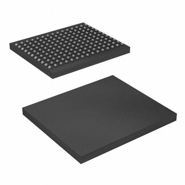
| 供应商器件封装 | 100-TQFP(14x20) |
| 其它名称 | CY7C1380D250AXC |
| 包装 | 托盘 |
| 商标 | Cypress Semiconductor |
| 存储器类型 | SRAM - 同步 |
| 存储容量 | 18 Mbit |
| 存储类型 | SDR |
| 安装风格 | SMD/SMT |
| 封装 | Tray |
| 封装/外壳 | 100-LQFP |
| 封装/箱体 | TQFP-100 |
| 工作温度 | 0°C ~ 70°C |
| 工厂包装数量 | 72 |
| 接口 | Parallel |
| 最大工作温度 | + 70 C |
| 最大工作电流 | 70 mA |
| 最大时钟频率 | 250 MHz |
| 最小工作温度 | 0 C |
| 标准包装 | 72 |
| 格式-存储器 | RAM |
| 电压-电源 | 3.135 V ~ 3.6 V |
| 电源电压-最大 | 3.6 V |
| 电源电压-最小 | 3.135 V |
| 类型 | Synchronous |
| 系列 | CY7C1380D |
| 组织 | 512 k x 36 |
| 访问时间 | 2.6 ns |
| 速度 | 250MHz |


- 商务部:美国ITC正式对集成电路等产品启动337调查
- 曝三星4nm工艺存在良率问题 高通将骁龙8 Gen1或转产台积电
- 太阳诱电将投资9.5亿元在常州建新厂生产MLCC 预计2023年完工
- 英特尔发布欧洲新工厂建设计划 深化IDM 2.0 战略
- 台积电先进制程称霸业界 有大客户加持明年业绩稳了
- 达到5530亿美元!SIA预计今年全球半导体销售额将创下新高
- 英特尔拟将自动驾驶子公司Mobileye上市 估值或超500亿美元
- 三星加码芯片和SET,合并消费电子和移动部门,撤换高东真等 CEO
- 三星电子宣布重大人事变动 还合并消费电子和移动部门
- 海关总署:前11个月进口集成电路产品价值2.52万亿元 增长14.8%

_renders/MR4A16BCYS35.jpg)

_renders/IS66WVE4M16EBLL-70BLI.jpg)

PDF Datasheet 数据手册内容提取
CY7C1380D CY7C1380F CY7C1382D 18-Mbit (512K × 36/1M × 18) Pipelined SRAM 18-Mbit (512K × 36/1M × 18) Pipelined SRAM Features Functional Description ■Supports bus operation up to 250 MHz The CY7C1380D/CY7C1380F/CY7C1382D SRAM integrates 524,288 × 36 and 1,048,576 × 18 SRAM cells with advanced ■Available speed grades are 250, 200, and 167 MHz synchronous peripheral circuitry and a two-bit counter for ■Registered inputs and outputs for pipelined operation internal burst operation. All synchronous inputs are gated by registers controlled by a positive edge triggered clock input ■3.3 V core power supply (CLK). The synchronous inputs include all addresses, all data ■2.5 V or 3.3 V I/O power supply inputs, address-pipelining chip enable (CE1), depth-expansion . chip enables (CE2 and CE3), burst control inputs (ADSC, ADSP, s ■Fast clock-to-output times and ADV), write enables (BW , and BWE), and global write n X ❐2.6 ns (for 250 MHz device) (GW). Asynchronous inputs include the output enable (OE) and g ■Provides high performance 3-1-1-1 access rate the ZZ pin. si e ■User selectable burst counter supporting Intel®Pentium® Addresses and chip enables are registered at rising edge of D clock when address strobe processor (ADSP) or address strobe interleaved or linear burst sequences controller (ADSC) are active. Subsequent burst addresses can w ■Separate processor and controller address strobes be internally generated as they are controlled by the advance pin e ■Synchronous self-timed write (ADV). N Address, data inputs, and write controls are registered on-chip ■Asynchronous output enable r to initiate a self-timed write cycle. This part supports byte write o ■Single cycle chip deselect operations (see Pin Definitions on page 6 and Truth Table on f page 10 for further details). Write cycles can be one to two or four d ■CY7C1380D/CY7C1382D is available in JEDEC-standard bytes wide as controlled by the byte write control inputs. GW e Pb-free 100-pin TQFP package; CY7C1380F is available in d when active LOW causes all bytes to be written. non Pb-free 165-ball FBGA package n The CY7C1380D/CY7C1380F/CY7C1382D operates from a e ■IEEE 1149.1 JTAG-Compatible Boundary Scan +3.3 V core power supply while all outputs operate with a +2.5 m ■ZZ sleep mode option or +3.3 V power supply. All inputs and outputs are m JEDEC-standard and JESD8-5-compatible. o For a complete list of related documentation, click here. c e R Selection Guide t o Description 250 MHz 200 MHz 167 MHz Unit N Maximum Access Time 2.6 3.0 3.4 ns Maximum Operating Current 350 300 275 mA Maximum CMOS Standby Current 70 70 70 mA Errata: For information on silicon errata, see “Errata” on page32. Details include trigger conditions, devices affected, and proposed workaround. CypressSemiconductorCorporation • 198 Champion Court • SanJose, CA 95134-1709 • 408-943-2600 Document Number: 38-05543 Rev. *S Revised March 29, 2016
CY7C1380D CY7C1380F CY7C1382D Logic Block Diagram – CY7C1380D/CY7C1380F A0, A1, A ADDRESS REGISTER 2 A[1:0] MODE ADV Q1 CLK BURST COUNTER CLR AND Q0 LOGIC ADSC ADSP DQD ,DQPD DQD ,DQPD BWD BYTE BYTE WRITE REGISTER WRITE DRIVER BBWWCB WWRRDDIITTQQEEB BC BRRY Y,,EEDTDTGGEQEQIISPSPTTCEBERR WWDDRRQIIQTTBBEECBY Y ,DD,DTTDRREEQQIIVVPPEECBRR MAERMROARYY SAEMNPSSE ROEGUITSPTUERTS BOUUFTFPEEURTS DDDDDQQQQQPPPPsADBC signs. DQA ,DQPA DQBAY ,DTEQPA e BBWWEA WRITEB RYETGEISTER WRITE DRIVER D INPUT GCCCWEEE123 REENGAISBTLEER PEIPNEALIBNLEED REGISTERS ew OE N ZZ COSNLETERPOL or f d e Logic Block Diagram – CY7C1382D d n e ADDRESS m A0, A1, A REGISTER 2 m o ADV BURST Q1 CLK COUNTER AND c LOGIC e R ADSC t o DQB,DQPB DQB,DQPB N BWB WRITE REGISTER WRITE DRIVER MAERMROARYY SENSE OUTPUT BOUUFTFPEURTS DDQQsPA DQA,DQPA DQPB BWA WRIDTQE RAE,DGQISPTEAR WRITE DRIVER BWE INPUT GW ENABLE CE1 REGISTER PIPELINED CE2 ENABLE CE3 OE ZZ SLEEP CONTROL Document Number: 38-05543 Rev. *S Page 2 of 38
CY7C1380D CY7C1380F CY7C1382D Contents Pin Configurations ...........................................................4 Scan Register Sizes .......................................................18 Pin Definitions ..................................................................6 Identification Codes .......................................................18 Functional Overview ........................................................8 Boundary Scan Order ....................................................19 Single Read Accesses ................................................8 Maximum Ratings ...........................................................20 Single Write Accesses Initiated by ADSP ...................8 Operating Range .............................................................20 Single Write Accesses Initiated by ADSC ...................8 Electrical Characteristics ...............................................20 Burst Sequences .........................................................8 Capacitance ....................................................................21 Sleep Mode .................................................................9 Thermal Resistance ........................................................21 Interleaved Burst Address Table .................................9 AC Test Loads and Waveforms .....................................22 Linear Burst Address Table .........................................9 Switching Characteristics ..............................................23 ZZ Mode Electrical Characteristics ..............................9 Switching Waveforms ....................................................24 Truth Table ......................................................................10 Ordering Information ......................................................28 . Truth Table for Read/Write ............................................11 Ordering Code Definitions .........................................28 s Truth Table for Read/Write ............................................11 Package Diagrams ..........................................................29 n g IEEE 1149.1 Serial Boundary Scan (JTAG [13]) ...........12 Acronyms ........................................................................31 i Disabling the JTAG Feature ......................................12 Document Conventions .................................................31 s Test Access Port (TAP) .............................................12 Units of Measure .......................................................31 e D PERFORMING A TAP RESET ..................................12 Errata ...............................................................................32 TAP REGISTERS ......................................................12 Part Numbers Affected ..............................................32 w TAP Instruction Set ...................................................13 Product Status ...........................................................32 e TAP Controller State Diagram .......................................14 Ram9 Sync ZZ Pin N TAP Controller Block Diagram ......................................15 & JTAG Issues Errata Summary ......................................32 TAP Timing ......................................................................16 Document History Page .................................................34 r o TAP AC Switching Characteristics ...............................16 Sales, Solutions, and Legal Information ......................38 f 3.3 V TAP AC Test Conditions .......................................17 Worldwide Sales and Design Support .......................38 d 3.3 V TAP AC Output Load Equivalent .........................17 Products ....................................................................38 e 2.5 V TAP AC Test Conditions .......................................17 PSoC® Solutions ......................................................38 d 2.5 V TAP AC Output Load Equivalent .........................17 Cypress Developer Community .................................38 n TAP DC Electrical Characteristics Technical Support .....................................................38 e and Operating Conditions .............................................17 m Identification Register Definitions ................................18 m o c e R t o N Document Number: 38-05543 Rev. *S Page 3 of 38
CY7C1380D CY7C1380F CY7C1382D Pin Configurations Figure 1. 100-pin TQFP (14 × 20 × 1.4 mm) pinout (3-Chip Enable) [1] CY7C1380D (512K × 36) CY7C1382D (1M × 18) . s n g i s e D w e N r o f d e d n e m m o c e R t o N Note 1. Errata: The ZZ pin (Pin 64) needs to be externally connected to ground. For more information, see “Errata” on page32. Document Number: 38-05543 Rev. *S Page 4 of 38
CY7C1380D CY7C1380F CY7C1382D Pin Configurations (continued) Figure 2. 165-ball FBGA (13 × 15 × 1.4 mm) pinout (3-Chip Enable) [2, 3] CY7C1380F (512K × 36) 1 2 3 4 5 6 7 8 9 10 11 A NC/288M A CE1 BWC BWB CE3 BWE ADSC ADV A NC B NC/144M A CE2 BWD BWA CLK GW OE ADSP A NC/576M C DQP NC V V V V V V V NC/1G DQP C DDQ SS SS SS SS SS DDQ B D DQ DQ V V V V V V V DQ DQ C C DDQ DD SS SS SS DD DDQ B B E DQ DQ V V V V V V V DQ DQ C C DDQ DD SS SS SS DD DDQ B B F DQ DQ V V V V V V V DQ DQ C C DDQ DD SS SS SS DD DDQ B B . G DQ DQ V V V V V V V DQ DQ s C C DDQ DD SS SS SS DD DDQ B B n H NC NC NC V V V V V NC NC ZZ DD SS SS SS DD g J DQ DQ V V V V V V V DQ DQ i D D DDQ DD SS SS SS DD DDQ A A s K DQ DQ V V V V V V V DQ DQ e D D DDQ DD SS SS SS DD DDQ A A D L DQ DQ V V V V V V V DQ DQ D D DDQ DD SS SS SS DD DDQ A A M DQ DQ V V V V V V V DQ DQ w D D DDQ DD SS SS SS DD DDQ A A N DQP NC V V NC A NC V V NC DQP e D DDQ SS SS DDQ A N P NC NC/72M A A TDI A1 TDO A A A A r R MODE NC/36M A A TMS A0 TCK A A A A o f d e d n e m m o c e R t o N Notes 2. Errata: The ZZ ball (H11) needs to be externally connected to ground. For more information, see “Errata” on page32. 3. Errata: The JTAG testing should be performed with these devices in BYPASS mode as the JTAG functionality is not guaranteed. For more information, see “Errata” on page32. Document Number: 38-05543 Rev. *S Page 5 of 38
CY7C1380D CY7C1380F CY7C1382D Pin Definitions Name I/O Description A , A , A Input- Address inputs used to select one of the address locations. Sampled at the rising edge of the CLK 0 1 Synchronous if ADSP or ADSC is active LOW, and CE ,CE , andCE are sampled active. A1:A0 are fed to the two-bit 1 2 3 counter. BW , BW , Input- Byte write select inputs, active LOW. Qualified with BWE to conduct byte writes to the SRAM. Sampled A B BW , BW Synchronous on the rising edge of CLK. C D GW Input- Global write enable input, active LOW. When asserted LOW on the rising edge of CLK, a global write Synchronous is conducted (all bytes are written, regardless of the values on BW and BWE). X BWE Input- Byte write enable input, active LOW. Sampled on the rising edge of CLK. This signal must be asserted Synchronous LOW to conduct a byte write. . s CLK Input- Clock input. Used to capture all synchronous inputs to the device. Also used to increment the burst n Clock counter when ADV is asserted LOW, during a burst operation. g CE1 Input- Chip enable 1 input, active LOW. Sampled on the rising edge of CLK. Used in conjunction with CE2 si Synchronous and CE to select or deselect the device. ADSP is ignored if CE is HIGH. CE is sampled only when a e 3 1 1 new external address is loaded. D CE Input- Chip enable 2 input, active HIGH. Sampled on the rising edge of CLK. Used in conjunction with CE 2 1 w Synchronous and CE to select or deselect the device. CE is sampled only when a new external address is loaded. 3 2 e CE3 Input- Chip enable 3 input, active LOW. Sampled on the rising edge of CLK. Used in conjunction with CE1 N Synchronous and CE to select or deselect the device. CE is sampled only when a new external address is loaded. 2 3 r OE Input- Output enable, asynchronous input, active LOW. Controls the direction of the I/O pins. When LOW, o Asynchronou the I/O pins behave as outputs. When deasserted HIGH, I/O pins are tri-stated, and act as input data f s pins. OE is masked during the first clock of a read cycle when emerging from a deselected state. d e ADV Input- Advance input signal, sampled on the rising edge of CLK, active LOW. When asserted, it d Synchronous automatically increments the address in a burst cycle. n ADSP Input- Address strobe from processor, sampled on the rising edge of CLK, active LOW. When asserted e Synchronous LOW, addresses presented to the device are captured in the address registers. A1:A0 are also loaded m into the burst counter. When ADSP and ADSC are both asserted, only ADSP is recognized. ASDP is m ignored when CE is deasserted HIGH. 1 o ADSC Input- Address strobe from controller, sampled on the rising edge of CLK, active LOW. When asserted c Synchronous LOW, addresses presented to the device are captured in the address registers. A1:A0 are also loaded e into the burst counter. When ADSP and ADSC are both asserted, only ADSP is recognized. R ZZ [4] Input- ZZ sleep input. This active HIGH input places the device in a non-time critical sleep condition with data Asynchronou integrity preserved. For normal operation, this pin has to be LOW or left floating. ZZpin has an internal t o s pull down. N DQs, I/O- Bidirectional data I/O lines. As inputs, they feed into an on-chip data register that is triggered by the DQP Synchronous rising edge of CLK. As outputs, they deliver the data contained in the memory location specified by the X addresses presented during the previous clock rise of the read cycle. The direction of the pins is controlled by OE. When OE is asserted LOW, the pins behave as outputs. When HIGH, DQs and DQP X are placed in a tri-state condition. V Power Supply Power supply inputs to the core of the device DD V Ground Ground for the core of the device. SS V I/O Ground Ground for the I/O circuitry. SSQ V I/O Power Power supply for the I/O circuitry. DDQ Supply MODE Input-Static Selects burst order. When tied to GND selects linear burst sequence. When tied to V or left floating DD selects interleaved burst sequence. This is a strap pin and must remain static during device operation. Mode pin has an internal pull up. Note 4. Errata: The ZZ pin needs to be externally connected to ground. For more information, see “Errata” on page32. Document Number: 38-05543 Rev. *S Page 6 of 38
CY7C1380D CY7C1380F CY7C1382D Pin Definitions (continued) Name I/O Description TDO [5] JTAG serial Serial data-out to the JTAG circuit. Delivers data on the negative edge of TCK. If the JTAG feature is output not being utilized, this pin must be disconnected. This pin is not available on TQFP packages. Synchronous TDI [5] JTAG serial Serial data-in to the JTAG circuit. Sampled on the rising edge of TCK. If the JTAG feature is not being input utilized, this pin can be disconnected or connected to V . This pin is not available on TQFP packages. DD Synchronous TMS [5] JTAG serial Serial data-in to the JTAG circuit. Sampled on the rising edge of TCK. If the JTAG feature is not being input utilized, this pin can be disconnected or connected to V . This pin is not available on TQFP packages. DD Synchronous TCK [5] JTAG- Clock input to the JTAG circuitry. If the JTAG feature is not being utilized, this pin must be connected Clock to V . This pin is not available on TQFP packages. . SS s NC – No Connects. 36M, 72M, 144M, 288M, 576M, and 1G are address expansion pins and are not internally n connected to the die. g i s e D w e N r o f d e d n e m m o c e R t o N Note 5. Errata: The JTAG testing should be performed with these devices in BYPASS mode as the JTAG functionality is not guaranteed. For more information, see “Errata” on page32. Document Number: 38-05543 Rev. *S Page 7 of 38
CY7C1380D CY7C1380F CY7C1382D Functional Overview The write signals (GW, BWE, and BW ) and ADV inputs are X ignored during this first cycle. All synchronous inputs pass through input registers controlled by ADSP triggered write accesses require two clock cycles to the rising edge of the clock. All data outputs pass through output complete. If GW is asserted LOW on the second clock rise, the registers controlled by the rising edge of the clock. Maximum data presented to the DQs inputs is written into the access delay from the clock rise (t ) is 2.6 ns (250 MHz device). CO corresponding address location in the memory array. If GW is CY7C1380D/CY7C1380F/CY7C1382D supports secondary HIGH, then the write operation is controlled by BWE and BW X cache in systems using a linear or interleaved burst sequence. signals. The interleaved burst order supports Pentium and i486 CY7C1380D/CY7C1380F/CY7C1382D provides byte write processors. The linear burst sequence suits processors that use capability that is described in the write cycle descriptions table. a linear burst sequence. The burst order is user selectable, and Asserting the byte write enable input (BWE) with the selected is determined by sampling the MODE input. Accesses can be byte write (BW ) input, selectively writes to only the desired initiated with either the processor address strobe (ADSP) or the X bytes. Bytes not selected during a byte write operation remain controller address strobe (ADSC). Address advancement . unaltered. A synchronous self-timed write mechanism has been s through the burst sequence is controlled by the ADV input. A provided to simplify the write operations. n two-bit on-chip wraparound burst counter captures the first g address in a burst sequence and automatically increments the CY7C1380D/CY7C1380F/CY7C1382D is a common I/O device, i address for the rest of the burst access. the output enable (OE) must be deserted HIGH before s e presenting data to the DQs inputs. Doing so tri-states the output Byte write operations are qualified with the byte write enable D drivers. As a safety precaution, DQs are automatically tri-stated (BWE) and byte write select (BWX) inputs. A global write enable whenever a write cycle is detected, regardless of the state of OE. w (GW) overrides all byte write inputs and writes data to all four bytes. All writes are simplified with on-chip synchronous Single Write Accesses Initiated by ADSC e self-timed write circuitry. N ADSC write accesses are initiated when the following conditions Three synchronous chip selects (CE , CE , CE ) and an r 1 2 3 are satisfied: (1) ADSC is asserted LOW, (2) ADSP is deserted o asynchronous output enable (OE) provide for easy bank selection and output tri-state control. ADSP is ignored if CE is HIGH, (3) CE1, CE2, and CE3 are all asserted active, and (4) the f 1 appropriate combination of the write inputs (GW, BWE, and d HIGH. BW ) are asserted active to conduct a write to the desired e X byte(s). ADSC-triggered Write accesses require a single clock d Single Read Accesses cycle to complete. The address presented to A is loaded into the n This access is initiated when the following conditions are address register and the address advancement logic while being e satisfied at clock rise: (1) ADSP or ADSC is asserted LOW, delivered to the memory array. The ADV input is ignored during m (2)CE1, CE2, CE3 are all asserted active, and (3) the write this cycle. If a global write is conducted, the data presented to m signals (GW, BWE) are all deserted HIGH. ADSP is ignored if the DQs is written into the corresponding address location in the o CE is HIGH. The address presented to the address inputs (A) memory core. If a byte write is conducted, only the selected bytes c 1 is stored into the address advancement logic and the address are written. Bytes not selected during a byte write operation e register while being presented to the memory array. The remain unaltered. A synchronous self-timed write mechanism R corresponding data is enabled to propagate to the input of the has been provided to simplify the write operations. t output registers. At the rising edge of the next clock, the data is CY7C1380D/CY7C1380F/CY7C1382D is a common I/O device, o N enabled to propagate through the output register and onto the the output enable (OE) must be deserted HIGH before data bus within 2.6 ns (250 MHz device) if OE is active LOW. The presenting data to the DQs inputs. Doing so tri-states the output only exception occurs when the SRAM is emerging from a drivers. As a safety precaution, DQs are automatically tri-stated deselected state to a selected state; its outputs are always whenever a write cycle is detected, regardless of the state of OE. tri-stated during the first cycle of the access. After the first cycle of the access, the outputs are controlled by the OE signal. Burst Sequences Consecutive single read cycles are supported. Once the SRAM CY7C1380D/CY7C1380F/CY7C1382D provides a two-bit is deselected at clock rise by the chip select and either ADSP or wraparound counter, fed by A1:A0, that implements an ADSC signals, its output tri-states immediately. interleaved or a linear burst sequence. The interleaved burst Single Write Accesses Initiated by ADSP sequence is designed specifically to support Intel Pentium applications. The linear burst sequence is designed to support This access is initiated when both the following conditions are processors that follow a linear burst sequence. The burst satisfied at clock rise: (1) ADSP is asserted LOW and (2)CE , 1 sequence is user selectable through the MODE input. CE , and CE are all asserted active. The address presented to 2 3 A is loaded into the address register and the address Asserting ADV LOW at clock rise automatically increments the advancement logic while being delivered to the memory array. burst counter to the next address in the burst sequence. Both read and write burst operations are supported. Document Number: 38-05543 Rev. *S Page 8 of 38
CY7C1380D CY7C1380F CY7C1382D Sleep Mode The ZZ input pin is an asynchronous input. Asserting ZZ places Linear Burst Address Table the SRAM in a power conservation sleep mode. Two clock cycles (MODE = GND) are required to enter into or exit from this sleep mode. While in First Second Third Fourth this mode, data integrity is guaranteed. Accesses pending when Address Address Address Address entering the sleep mode are not considered valid nor is the A1:A0 A1:A0 A1:A0 A1:A0 completion of the operation guaranteed. The device must be 00 01 10 11 deselected prior to entering the sleep mode. CE , CE , CE , 1 2 3 ADSP, and ADSC must remain inactive for the duration of t 01 10 11 00 ZZREC after the ZZ input returns LOW. 10 11 00 01 11 00 01 10 Interleaved Burst Address Table (MODE = Floating or V ) . DD s n First Second Third Fourth Address Address Address Address g A1:A0 A1:A0 A1:A0 A1:A0 si 00 01 10 11 e D 01 00 11 10 10 11 00 01 w e 11 10 01 00 N r o ZZ Mode Electrical Characteristics f d Parameter Description Test Conditions Min Max Unit e d I Sleep mode standby current ZZ > V – 0.2 V – 80 mA DDZZ DD n tZZS Device operation to ZZ ZZ > VDD – 0.2 V – 2tCYC ns e m t ZZ recovery time ZZ < 0.2 V 2t – ns ZZREC CYC m t ZZ Active to sleep current This parameter is sampled – 2t ns ZZI CYC o t ZZ Inactive to exit sleep current This parameter is sampled 0 – ns RZZI c e R t o N Document Number: 38-05543 Rev. *S Page 9 of 38
CY7C1380D CY7C1380F CY7C1382D Truth Table The Truth Table for CY7C1380D/CY7C1380F/CY7C1382D follows. [6, 7, 8, 9, 10] Operation Add. Used CE CE CE ZZ ADSP ADSC ADV WRITE OE CLK DQ 1 2 3 Deselect Cycle, Power Down None H X X L X L X X X L–H Tri-state Deselect Cycle, Power Down None L L X L L X X X X L–H Tri-state Deselect Cycle, Power Down None L X H L L X X X X L–H Tri-state Deselect Cycle, Power Down None L L X L H L X X X L–H Tri-state Deselect Cycle, Power Down None L X H L H L X X X L–H Tri-state . Sleep Mode, Power Down None X X X H X X X X X X Tri-state s n READ Cycle, Begin Burst External L H L L L X X X L L–H Q g READ Cycle, Begin Burst External L H L L L X X X H L–H Tri-state si e WRITE Cycle, Begin Burst External L H L L H L X L X L–H D D READ Cycle, Begin Burst External L H L L H L X H L L–H Q w READ Cycle, Begin Burst External L H L L H L X H H L–H Tri-state e READ Cycle, Continue Burst Next X X X L H H L H L L–H Q N READ Cycle, Continue Burst Next X X X L H H L H H L–H Tri-state r o READ Cycle, Continue Burst Next H X X L X H L H L L–H Q f d READ Cycle, Continue Burst Next H X X L X H L H H L–H Tri-state e WRITE Cycle, Continue Burst Next X X X L H H L L X L–H D d n WRITE Cycle, Continue Burst Next H X X L X H L L X L–H D e m READ Cycle, Suspend Burst Current X X X L H H H H L L–H Q m READ Cycle, Suspend Burst Current X X X L H H H H H L–H Tri-state o READ Cycle, Suspend Burst Current H X X L X H H H L L–H Q c READ Cycle, Suspend Burst Current H X X L X H H H H L–H Tri-state e R WRITE Cycle, Suspend Burst Current X X X L H H H L X L–H D t WRITE Cycle, Suspend Burst Current H X X L X H H L X L–H D o N Notes 6. X = Don't Care, H = Logic HIGH, L = Logic LOW. 7. WRITE = L when any one or more byte write enable signals, and BWE = L or GW = L. WRITE = H when all byte write enable signals, BWE, GW = H. 8. The DQ pins are controlled by the current cycle and the OE signal. OE is asynchronous and is not sampled with the clock. 9. The SRAM always initiates a read cycle when ADSP is asserted, regardless of the state of GW, BWE, or BWX. Writes may occur only on subsequent clocks after the ADSP or with the assertion of ADSC. As a result, OE must be driven HIGH prior to the start of the write cycle to allow the outputs to tri-state. OE is a don't care for the remainder of the write cycle. 10.OE is asynchronous and is not sampled with the clock rise. It is masked internally during write cycles. During a read cycle all data bits are tri-state when OE is inactive or when the device is deselected, and all data bits behave as output when OE is active (LOW). Document Number: 38-05543 Rev. *S Page 10 of 38
CY7C1380D CY7C1380F CY7C1382D Truth Table for Read/Write The Truth Table for Read/Write for CY7C1380D/CY7C1380F follows. [11, 12] Function (CY7C1380D/CY7C1380F) GW BWE BW BW BW BW D C B A Read H H X X X X Read H L H H H H Write Byte A – (DQ and DQP ) H L H H H L A A Write Byte B – (DQ and DQP ) H L H H L H B B Write Bytes B, A H L H H L L . Write Byte C – (DQ and DQP ) H L H L H H s C C n Write Bytes C, A H L H L H L g Write Bytes C, B H L H L L H si e Write Bytes C, B, A H L H L L L D Write Byte D – (DQD and DQPD) H L L H H H w Write Bytes D, A H L L H H L e Write Bytes D, B H L L H L H N Write Bytes D, B, A H L L H L L r o Write Bytes D, C H L L L H H f d Write Bytes D, C, A H L L L H L e Write Bytes D, C, B H L L L L H d n Write All Bytes H L L L L L e m Write All Bytes L X X X X X m o c Truth Table for Read/Write e R The Truth Table for Read/Write for CY7C1382D follows. [11, 12] t Function (CY7C1382D) GW BWE BW BW o B A N Read H H X X Read H L H H Write Byte A – (DQ and DQP ) H L H L A A Write Byte B – (DQ and DQP ) H L L H B B Write Bytes B, A H L L L Write All Bytes H L L L Write All Bytes L X X X Notes 11.X = Don't Care, H = Logic HIGH, L = Logic LOW. 12.Table only lists a partial listing of the byte write combinations. Any combination of BWX is valid. Appropriate write is done based on which byte write is active. Document Number: 38-05543 Rev. *S Page 11 of 38
CY7C1380D CY7C1380F CY7C1382D IEEE 1149.1 Serial Boundary Scan (JTAG [13]) At power up, the TAP is reset internally to ensure that TDO comes up in a high Z state. The CY7C1380F incorporates a serial boundary scan test TAP Registers access port (TAP).This part is fully compliant with 1149.1. The TAP operates using JEDEC-standard 3.3 V or 2.5 V I/O logic Registers are connected between the TDI and TDO balls and levels. enable data to be scanned in and out of the SRAM test circuitry. CY7C1380F contains a TAP controller, instruction register, Only one register can be selected at a time through the boundary scan register, bypass register, and ID register. instruction register. Data is serially loaded into the TDI ball on the rising edge of TCK. Data is output on the TDO ball on the falling Disabling the JTAG Feature edge of TCK. It is possible to operate the SRAM without using the JTAG Instruction Register feature. To disable the TAP controller, TCK must be tied LOW Three-bit instructions can be serially loaded into the instruction (V ) to prevent clocking of the device. TDI and TMS are SS register. This register is loaded when it is placed between the TDI internally pulled up and may be unconnected. They may alternately be connected to VDD through a pull up resistor. TDO apangde T D15O. Ubaplolsn a pso swheorw unp i,n t hthee iTnAstPru Cctoionntr orellegris Btelor cisk Dloiaadgeradm w oithn s. must be left unconnected. Upon power up, the device comes up n the IDCODE instruction. It is also loaded with the IDCODE in a reset state which does not interfere with the operation of the g instruction if the controller is placed in a reset state as described device. i in the previous section. s Test Access Port (TAP) e When the TAP controller is in the Capture-IR state, the two least D significant bits are loaded with a binary ‘01’ pattern to enable fault Test Clock (TCK) isolation of the board-level serial test data path. w The test clock is used only with the TAP controller. All inputs are captured on the rising edge of TCK. All outputs are driven from Bypass Register e N the falling edge of TCK. To save time when serially shifting data through registers, it is sometimes advantageous to skip certain chips. The bypass r Test MODE SELECT (TMS) register is a single-bit register that can be placed between the o The TMS input is used to give commands to the TAP controller TDI and TDO balls. This enables data to be shifted through the f and is sampled on the rising edge of TCK. This pin may be left SRAM with minimal delay. The bypass register is set LOW (V ) d SS unconnected if the TAP is not used. The ball is pulled up when the BYPASS instruction is executed. e internally, resulting in a logic HIGH level. d Boundary Scan Register n Test Data-In (TDI) e The boundary scan register is connected to all the input and m The TDI ball is used to serially input information into the registers bidirectional balls on the SRAM. and can be connected to the input of any of the registers. The The boundary scan register is loaded with the contents of the m register between TDI and TDO is chosen by the instruction that RAM input and output ring when the TAP controller is in the o is loaded into the TAP instruction register. For information on Capture-DR state and is then placed between the TDI and TDO c loading the instruction register, see TAP Controller State balls when the controller is moved to the Shift-DR state. The e Diagram on page 14. TDI is internally pulled up and can be EXTEST, SAMPLE/PRELOAD, and SAMPLE Z instructions can R unconnected if the TAP is unused in an application. TDI is be used to capture the contents of the input and output ring. connected to the most significant bit (MSB) of any register. t The Boundary Scan Order on page 19 show the order in which o Test Data-Out (TDO) the bits are connected. Each bit corresponds to one of the bumps N on the SRAM package. The MSB of the register is connected to The TDO output ball is used to serially clock data-out from the TDI, and the LSB is connected to TDO. registers. The output is active depending upon the current state of the TAP state machine (see Identification Codes on page 18). Identification (ID) Register The output changes on the falling edge of TCK. TDO is connected to the least significant bit (LSB) of any register. The ID register is loaded with a vendor-specific 32-bit code during the Capture-DR state when the IDCODE command is Performing a TAP Reset loaded in the instruction register. The IDCODE is hardwired into the SRAM and can be shifted out when the TAP controller is in A Reset is performed by forcing TMS HIGH (V ) for five rising DD the Shift-DR state. The ID register has a vendor code and other edges of TCK. This Reset does not affect the operation of the information described in the Identification Register Definitions on SRAM and may be performed while the SRAM is operating. page 18. Note 13.Errata: The JTAG testing should be performed with these devices in BYPASS mode as the JTAG functionality is not guaranteed. For more information, see “Errata” on page32. Document Number: 38-05543 Rev. *S Page 12 of 38
CY7C1380D CY7C1380F CY7C1382D TAP Instruction Set To guarantee that the boundary scan register captures the correct value of a signal, the SRAM signal must be stabilized Overview long enough to meet the TAP controller’s capture setup plus hold Eight different instructions are possible with the three bit times (tCS and tCH). The SRAM clock input might not be captured instruction register. All combinations are listed in Identification correctly if there is no way in a design to stop (or slow) the clock Codes on page 18. Three of these instructions are listed as during a SAMPLE/PRELOAD instruction. If this is an issue, it is RESERVED and must not be used. The other five instructions still possible to capture all other signals and simply ignore the are described in detail in this section. value of the CK and CK# captured in the boundary scan register. Instructions are loaded into the TAP controller during the Shift-IR Once the data is captured, it is possible to shift out the data by state when the instruction register is placed between TDI and putting the TAP into the Shift-DR state. This places the boundary TDO. During this state, instructions are shifted through the scan register between the TDI and TDO pins. instruction register through the TDI and TDO balls. To execute PRELOAD enables an initial data pattern to be placed at the the instruction once it is shifted in, the TAP controller must be latched parallel outputs of the boundary scan register cells prior moved into the Update-IR state. to the selection of another boundary scan test operation. . EXTEST The shifting of data for the SAMPLE and PRELOAD phases can s occur concurrently when required; that is, while data captured is n The EXTEST instruction enables the preloaded data to be driven shifted out, the preloaded data is shifted in. g out through the system output pins. This instruction also selects i s the boundary scan register to be connected for serial access BYPASS e between the TDI and TDO in the Shift-DR controller state. When the BYPASS instruction is loaded in the instruction register D and the TAP is placed in a Shift-DR state, the bypass register is IDCODE placed between the TDI and TDO balls. The advantage of the w The IDCODE instruction causes a vendor-specific 32-bit code to BYPASS instruction is that it shortens the boundary scan path e be loaded into the instruction register. It also places the when multiple devices are connected together on a board. N instruction register between the TDI and TDO balls and enables the IDCODE to be shifted out of the device when the TAP EXTEST Output Bus Tri-State r controller enters the Shift-DR state. o IEEE Standard 1149.1 mandates that the TAP controller be able f The IDCODE instruction is loaded into the instruction register to put the output bus into a tri-state mode. d upon power up or whenever the TAP controller is given a test The boundary scan register has a special bit located at Bit #89 e logic reset state. (for 165-ball FBGA package). When this scan cell, called the d “extest output bus tri-state,” is latched into the preload register n SAMPLE Z during the Update-DR state in the TAP controller, it directly e The SAMPLE Z instruction causes the boundary scan register to controls the state of the output (Q-bus) pins, when the EXTEST m be connected between the TDI and TDO balls when the TAP is entered as the current instruction. When HIGH, it enables the controller is in a Shift-DR state. The SAMPLE Z command places output buffers to drive the output bus. When LOW, this bit places m all SRAM outputs into a high Z state. the output bus into a high Z condition. o c SAMPLE/PRELOAD This bit can be set by entering the SAMPLE/PRELOAD or e EXTEST command, and then shifting the desired bit into that cell, SAMPLE/PRELOAD is a 1149.1 mandatory instruction. When R during the Shift-DR state. During Update-DR, the value loaded tinhset ruScAtioMnP rLeEg/isPtRerE aLnOdA tDh e iTnAsPtru ccotinotnrosl lear ries inlo tahdee Cd apintutore -DthRe itnhteo EthXaTt EshSifTt- rinesgtirsutecrti ocenl li sla etcnhteesre idn,t ot hthise bpirt edloiraedc trlye gcisotnetrr.o Wls htehne ot state, a snapshot of data on the input and output pins is captured output Q-bus pins. Note that this bit is preset HIGH to enable the N in the boundary scan register. output when the device is powered up, and also when the TAP The TAP controller clock can only operate at a frequency up to controller is in the Test-Logic-Reset state. 20 MHz, while the SRAM clock operates more than an order of magnitude faster. As there is a large difference in the clock Reserved frequencies, it is possible that during the Capture-DR state, an These instructions are not implemented but are reserved for input or output undergoes a transition. The TAP may then try to future use. Do not use these instructions. capture a signal while in transition (metastable state). This does not harm the device, but there is no guarantee as to the value that is captured. Repeatable results may not be possible. Document Number: 38-05543 Rev. *S Page 13 of 38
CY7C1380D CY7C1380F CY7C1382D TAP Controller State Diagram TEST-LOGIC 1 RESET 0 RUN-TEST/ 1 SELECT 1 SELECT 1 0 IDLE DR-SCAN IR-SCAN 0 0 1 1 CAPTURE-DR CAPTURE-IR 0 0 . SHIFT-DR 0 SHIFT-IR 0 s n 1 1 g i 1 1 s EXIT1-DR EXIT1-IR e D 0 0 w PAUSE-DR 0 PAUSE-IR 0 e N 1 1 r 0 0 o EXIT2-DR EXIT2-IR f d 1 1 e d UPDATE-DR UPDATE-IR n e 1 0 1 0 m m o c e R The 0 or 1 next to each state represents the value of TMS at the rising edge of TCK. t o N Document Number: 38-05543 Rev. *S Page 14 of 38
CY7C1380D CY7C1380F CY7C1382D TAP Controller Block Diagram 0 Bypass Register 2 1 0 Selection Instruction Register TDI Circuitry Selection TDO 313029 . . . 2 1 0 Circuitry Identification Register . s x . . . . . 2 1 0 n g Boundary Scan Register i s e D w TCK e N TMS TAP CONTROLLER r o f d e d n e m m o c e R t o N Document Number: 38-05543 Rev. *S Page 15 of 38
CY7C1380D CY7C1380F CY7C1382D TAP Timing Figure 3. TAP Timing Test Clock (TCK) tTH tTL tCYC tTMSS tTMSH Test Mode Select (TMS) tTDIS tTDIH . Test Data-In s n (TDI) tTDOV g i s tTDOX Test Data-Out e D (TDO) w DON’T CARE UNDEFINED e N r TAP AC Switching Characteristics o f Over the Operating Range d e Parameter [14, 15] Description Min Max Unit d Clock n e t TCK Clock Cycle Time 50 – ns TCYC m t TCK Clock Frequency – 20 MHz TF m t TCK Clock HIGH time 20 – ns TH o tTL TCK Clock LOW time 20 – ns c Output Times e R t TCK Clock LOW to TDO Valid – 10 ns TDOV tTDOX TCK Clock LOW to TDO Invalid 0 – ns ot Setup Times N t TMS Setup to TCK Clock Rise 5 – ns TMSS t TDI Setup to TCK Clock Rise 5 – ns TDIS t Capture Setup to TCK Rise 5 – ns CS Hold Times t TMS Hold after TCK Clock Rise 5 – ns TMSH t TDI Hold after Clock Rise 5 – ns TDIH t Capture Hold after Clock Rise 5 – ns CH Notes 14.tCS and tCH refer to the setup and hold time requirements of latching data from the boundary scan register. 15.Test conditions are specified using the load in TAP AC test conditions. tR/tF = 1 ns. Document Number: 38-05543 Rev. *S Page 16 of 38
CY7C1380D CY7C1380F CY7C1382D 3.3 V TAP AC Test Conditions 2.5 V TAP AC Test Conditions Input pulse levels ...............................................V to 3.3 V Input pulse levels ...............................................V to 2.5 V SS SS Input rise and fall times ...................................................1 ns Input rise and fall time ....................................................1 ns Input timing reference levels .........................................1.5 V Input timing reference levels .......................................1.25 V Output reference levels ................................................1.5 V Output reference levels ..............................................1.25 V Test load termination supply voltage ............................1.5 V Test load termination supply voltage ..........................1.25 V 3.3 V TAP AC Output Load Equivalent 2.5 V TAP AC Output Load Equivalent 1.5V 1.25V 50Ω 50Ω . s TDO TDO n Z O = 50Ω 20pF Z O = 50Ω 20pF g i s e D w TAP DC Electrical Characteristics and Operating Conditions e N (0 °C < T < +70 °C; V = 3.3 V ± 0.165 V unless otherwise noted) A DD r Parameter [16] Description Test Conditions Min Max Unit o f VOH1 Output HIGH Voltage IOH = –4.0 mA, VDDQ = 3.3 V 2.4 – V d I = –1.0 mA, V = 2.5 V 2.0 – V e OH DDQ d VOH2 Output HIGH Voltage IOH = –100 µA VDDQ = 3.3 V 2.9 – V n V = 2.5 V 2.1 – V e DDQ m V Output LOW Voltage I = 8.0 mA V = 3.3 V – 0.4 V OL1 OL DDQ m V = 2.5 V – 0.4 V DDQ o VOL2 Output LOW Voltage IOL = 100 µA VDDQ = 3.3 V – 0.2 V c e V = 2.5 V – 0.2 V DDQ R V Input HIGH Voltage V = 3.3 V 2.0 V + 0.3 V IH DDQ DD t V = 2.5 V 1.7 V + 0.3 V o DDQ DD N V Input LOW Voltage V = 3.3 V –0.3 0.8 V IL DDQ V = 2.5 V –0.3 0.7 V DDQ I Input Load Current GND < V < V –5 5 µA X IN DDQ Note 16.All voltages referenced to VSS (GND). Document Number: 38-05543 Rev. *S Page 17 of 38
CY7C1380D CY7C1380F CY7C1382D Identification Register Definitions Instruction Field CY7C1380F (512K × 36) Description Revision Number (31:29) 000 Describes the version number. Device Depth (28:24) [17] 01011 Reserved for internal use. Device Width (23:18) 165-ball FBGA 000000 Defines the memory type and architecture. Cypress Device ID (17:12) 100101 Defines the width and density. Cypress JEDEC ID Code (11:1) 00000110100 Allows unique identification of SRAM vendor. ID Register Presence Indicator (0) 1 Indicates the presence of an ID register. . s Scan Register Sizes n g Register Name Bit Size (× 36) i s Instruction 3 e Bypass 1 D ID 32 w Boundary Scan Order (165-ball FBGA package) 89 e N r Identification Codes o f Instruction Code Description d e EXTEST 000 Captures I/O ring contents. Places the boundary scan register between TDI and TDO. Forces d all SRAM outputs to high Z state. n IDCODE 001 Loads the ID register with the vendor ID code and places the register between TDI and TDO. e This operation does not affect SRAM operations. m SAMPLE Z 010 Captures I/O ring contents. Places the boundary scan register between TDI and TDO. Forces m all SRAM output drivers to a high Z state. o RESERVED 011 Do Not Use. This instruction is reserved for future use. c SAMPLE/PRELOAD 100 Captures I/O ring contents. Places the boundary scan register between TDI and TDO. Does e not affect SRAM operation. R RESERVED 101 Do Not Use. This instruction is reserved for future use. t o RESERVED 110 Do Not Use. This instruction is reserved for future use. N BYPASS 111 Places the bypass register between TDI and TDO. This operation does not affect SRAM operations. Note 17.Bit #24 is 1 in the register definitions for both 2.5 V and 3.3 V versions of this device. Document Number: 38-05543 Rev. *S Page 18 of 38
CY7C1380D CY7C1380F CY7C1382D Boundary Scan Order 165-ball BGA [18, 19] Bit # Ball ID Bit # Ball ID Bit # Ball ID 1 N6 31 D10 61 G1 2 N7 32 C11 62 D2 3 N10 33 A11 63 E2 4 P11 34 B11 64 F2 5 P8 35 A10 65 G2 6 R8 36 B10 66 H1 7 R9 37 A9 67 H3 s. 8 P9 38 B9 68 J1 n g 9 P10 39 C10 69 K1 i s 10 R10 40 A8 70 L1 e 11 R11 41 B8 71 M1 D 12 H11 42 A7 72 J2 w 13 N11 43 B7 73 K2 e 14 M11 44 B6 74 L2 N 15 L11 45 A6 75 M2 r o 16 K11 46 B5 76 N1 f 17 J11 47 A5 77 N2 d e 18 M10 48 A4 78 P1 d 19 L10 49 B4 79 R1 n 20 K10 50 B3 80 R2 e m 21 J10 51 A3 81 P3 m 22 H9 52 A2 82 R3 o 23 H10 53 B2 83 P2 c 24 G11 54 C2 84 R4 e R 25 F11 55 B1 85 P4 26 E11 56 A1 86 N5 t o 27 D11 57 C1 87 P6 N 28 G10 58 D1 88 R6 29 F10 59 E1 89 Internal 30 E10 60 F1 Note 18.Balls which are NC (No Connect) are pre-set LOW. 19.Bit# 89 is pre-set HIGH. Document Number: 38-05543 Rev. *S Page 19 of 38
CY7C1380D CY7C1380F CY7C1382D Maximum Ratings DC Input Voltage ................................–0.5 V to V + 0.5 V DD Current into Outputs (LOW) ........................................20 mA Exceeding the maximum ratings may impair the useful life of the Static Discharge Voltage device. For user guidelines, not tested. (per MIL-STD-883, Method 3015) ..........................> 2001 V Storage Temperature ...............................–65 °C to +150 °C Latch-up Current ....................................................> 200 mA Ambient Temperature with Power Applied .........................................–55 °C to +125 °C Operating Range Supply Voltage on V Relative to GND .....–0.3 V to +4.6 V DD Ambient Range V V Supply Voltage on VDDQ Relative to GND ....–0.3 V to +VDD Temperature DD DDQ DC Voltage Applied to Outputs Commercial 0 °C to +70 °C 3.3 V– 5% / 2.5 V – 5% to in tri-state ..........................................–0.5 V to VDDQ + 0.5 V Industrial –40 °C to +85 °C + 10% VDD Electrical Characteristics . s n Over the Operating Range g i Parameter [20, 21] Description Test Conditions Min Max Unit s e V Power Supply Voltage 3.135 3.6 V DD D VDDQ I/O Supply Voltage for 3.3 V I/O 3.135 VDD V w for 2.5 V I/O 2.375 2.625 V e VOH Output HIGH Voltage for 3.3 V I/O, IOH = –4.0 mA 2.4 – V N for 2.5 V I/O, I = –1.0 mA 2.0 – V OH r V Output LOW Voltage for 3.3 V I/O, I = 8.0 mA – 0.4 V o OL OL f for 2.5 V I/O, IOL = 1.0 mA – 0.4 V d V Input HIGH Voltage [20] for 3.3 V I/O 2.0 V + 0.3 V V e IH DD d for 2.5 V I/O 1.7 V + 0.3 V V DD n V Input LOW Voltage [20] for 3.3 V I/O –0.3 0.8 V e IL m for 2.5 V I/O –0.3 0.7 V m I Input Leakage Current except ZZ GND V V –5 5 A X I DDQ and MODE o Input Current of MODE Input = V –30 – A c SS e Input = VDD 5 A R Input Current of ZZ Input = VSS –5 – A t o Input = V 30 A DD N I Output Leakage Current GND V V Output Disabled –5 5 A OZ I DDQ, I V Operating Supply Current V = Max., I = 0 mA, 4.0-ns cycle, – 350 mA DD DD DD OUT f = f = 1/t 250 MHz MAX CYC 5.0-ns cycle, – 300 mA 200 MHz 6.0-ns cycle, – 275 mA 167 MHz I Automatic CE Power Down V = Max, Device Deselected, 4.0-ns cycle, – 160 mA SB1 DD Current – TTL Inputs V V or V V , 250 MHz IN IH IN IL f = f = 1/t MAX CYC 5.0-ns cycle, – 150 mA 200 MHz 6.0-ns cycle, – 140 mA 167 MHz Notes 20.Overshoot: VIH(AC) < VDD + 1.5 V (pulse width less than tCYC/2), undershoot: VIL(AC) > –2 V (pulse width less than tCYC/2). 21.TPower up: Assumes a linear ramp from 0 V to VDD(min.) within 200 ms. During this time VIH < VDD and VDDQ < VDD. Document Number: 38-05543 Rev. *S Page 20 of 38
CY7C1380D CY7C1380F CY7C1382D Electrical Characteristics (continued) Over the Operating Range Parameter [20, 21] Description Test Conditions Min Max Unit I Automatic CE Power Down V = Max, Device Deselected, All speeds – 70 mA SB2 DD Current – CMOS Inputs V 0.3 V or V > V – 0.3 IN IN DDQ V, f = 0 I Automatic CE Power Down V = Max, Device Deselected, 4.0-ns cycle, – 135 mA SB3 DD Current – CMOS Inputs V 0.3 V or V > V – 0.3 250 MHz IN IN DDQ V, 5.0-ns cycle, – 130 mA f = f = 1/t MAX CYC 200 MHz 6.0-ns cycle, – 125 mA 167 MHz . s I Automatic CE Power Down V = Max, Device Deselected, All speeds – 80 mA n SB4 DD Current – TTL Inputs V V or V V , f = 0 g IN IH IN IL i s e Capacitance D Parameter [22] Description Test Conditions 100-pin TQFP 165-ball FBGA Unit w Package Package e C Input capacitance T = 25 °C, f = 1 MHz, 5 9 pF N IN A CCLK Clock input capacitance VDD = 3.3 V, VDDQ = 2.5 V 5 9 pF r o CIO Input/Output capacitance 5 9 pF f d e d Thermal Resistance n e Parameter [22] Description Test Conditions 100-pin TQFP 165-ball FBGA Unit m Package Package Thermal resistance Test conditions follow standard test 28.66 20.7 °C/W m JA (junction to ambient) methods and procedures for measuring o Thermal resistance thermal impedance, in accordance with 4.08 4.0 °C/W c JC EIA/JESD51. e (junction to case) R t o N Note 22.Tested initially and after any design or process change that may affect these parameters. Document Number: 38-05543 Rev. *S Page 21 of 38
CY7C1380D CY7C1380F CY7C1382D AC Test Loads and Waveforms Figure 4. AC Test Loads and Waveforms 3.3 V I/O Test Load R = 317 OUTPUT 3.3 V ALL INPUT PULSES V OUTPUT DDQ 90% Z0= 50 90% RL= 50 10% 10% 5pF GND R = 351 1 ns 1 ns V = 1.5 V T INCLUDING (a) JIG AND (c) (b) SCOPE . s 2.5 V I/O Test Load R = 1667 n OUTPUT 2.5 V V ALL INPUT PULSES g DDQ OUTPUT 90% i Z0= 50 90% s RL= 50 10% 10% e 5pF GND D R = 1538 1 ns 1 ns V = 1.25 V T w INCLUDING JIG AND e (a) SCOPE (b) (c) N r o f d e d n e m m o c e R t o N Document Number: 38-05543 Rev. *S Page 22 of 38
CY7C1380D CY7C1380F CY7C1382D Switching Characteristics Over the Operating Range 250 MHz 200 MHz 167 MHz Parameter [23, 24] Description Unit Min Max Min Max Min Max t V (typical) to the first Access [25] 1 – 1 – 1 – ms POWER DD Clock t Clock Cycle Time 4.0 – 5 – 6 – ns CYC t Clock HIGH 1.7 – 2.0 – 2.2 – ns CH tCL Clock LOW 1.7 – 2.0 – 2.2 – ns . s Output Times n g t Data Output Valid After CLK Rise – 2.6 – 3.0 – 3.4 ns CO i s t Data Output Hold After CLK Rise 1.0 – 1.3 – 1.3 – ns DOH e t Clock to Low-Z [26, 27, 28] 1.0 – 1.3 – 1.3 – ns D CLZ tCHZ Clock to High-Z [26, 27, 28] – 2.6 – 3.0 – 3.4 ns w t OE LOW to Output Valid – 2.6 – 3.0 – 3.4 ns e OEV N t OE LOW to Output Low-Z [26, 27, 28] 0 – 0 – 0 – ns OELZ t OE HIGH to Output High-Z [26, 27, 28] – 2.6 – 3.0 – 3.4 ns r OEHZ o Setup Times f d t Address Setup Before CLK Rise 1.2 – 1.4 – 1.5 – ns AS e t ADSC, ADSP Setup Before CLK Rise 1.2 – 1.4 – 1.5 – ns d ADS n t ADV Setup Before CLK Rise 1.2 – 1.4 – 1.5 – ns ADVS e t GW, BWE, BW Setup Before CLK 1.2 – 1.4 – 1.5 – ns m WES X Rise m t Data Input Setup Before CLK Rise 1.2 – 1.4 – 1.5 – ns DS o t Chip Enable SetUp Before CLK Rise 1.2 – 1.4 – 1.5 – ns c CES e Hold Times R tAH Address Hold After CLK Rise 0.3 – 0.4 – 0.5 – ns t o t ADSP, ADSC Hold After CLK Rise 0.3 – 0.4 – 0.5 – ns ADH N t ADV Hold After CLK Rise 0.3 – 0.4 – 0.5 – ns ADVH t GW, BWE, BW Hold After CLK Rise 0.3 – 0.4 – 0.5 – ns WEH X t Data Input Hold After CLK Rise 0.3 – 0.4 – 0.5 – ns DH t Chip Enable Hold After CLK Rise 0.3 – 0.4 – 0.5 – ns CEH Notes 23.Timing reference level is 1.5 V when VDDQ = 3.3 V and is 1.25 V when VDDQ = 2.5 V. 24.Test conditions shown in (a) of Figure 4 on page 22 unless otherwise noted. 25.This part has a voltage regulator internally; tPOWER is the time that the power needs to be supplied above VDD(minimum) initially before a read or write operation can be initiated. 26.tCHZ, tCLZ, tOELZ, and tOEHZ are specified with AC test conditions shown in part (b) of Figure 4 on page 22. Transition is measured ±200mV from steady-state voltage. 27.At any given voltage and temperature, tOEHZ is less than tOELZ and tCHZ is less than tCLZ to eliminate bus contention between SRAMs when sharing the same data bus. These specifications do not imply a bus contention condition, but reflect parameters guaranteed over worst case user conditions. Device is designed to achieve high Z prior to low Z under the same system conditions. 28.This parameter is sampled and not 100% tested. Document Number: 38-05543 Rev. *S Page 23 of 38
CY7C1380D CY7C1380F CY7C1382D Switching Waveforms Figure 5. Read Cycle Timing [29] tCYC CLK tCH tCL t t ADS ADH ADSP . tADS tADH s n ADSC g i s tAS tAH e D ADDRESS A1 A2 A3 w Burst continued with tWES tWEH new base address e N GW, BWE, BWx r o tCES tCEH Dcyecsleelect f d CE e d tADVS tADVH n e ADV m ADV m suspends burst. o OE c tOEV tCO e tCLZ tOEHZ tOELZ tDOH tCHZ R t o Data Out (Q) High-Z Q(A1) Q(A2) Q(A2 + 1) Q(A2 + 2) Q(A2 + 3) Q(A2) Q(A2 + 1) tCO N Burst wraps around to its initial state Single READ BURST READ DON’T CARE UNDEFINED Note 29.On this diagram, when CE is LOW: CE1 is LOW, CE2 is HIGH and CE3 is LOW. When CE is HIGH: CE1 is HIGH or CE2 is LOW or CE3 is HIGH. Document Number: 38-05543 Rev. *S Page 24 of 38
CY7C1380D CY7C1380F CY7C1382D Switching Waveforms (continued) Figure 6. Write Cycle Timing [30, 31] tCYC CLK tCH tCL tADS tADH ADSP ADSC extends burst tADS tADH tADS tADH ADSC . s tAS tAH n g ADDRESS A1 A2 A3 i s Byte write signals are e ignored for first cycle when D ADSP initiates burst tWES tWEH BWE, w BWX e tWES tWEH N GW r o tCES tCEH f d CE e tADVS tADVH d n ADV e m ADV suspends burst m OE o tDS tDH c e R Data In (D) High-Z D(A1) D(A2) D(A2 + 1) D(A2 + 1) D(A2 + 2) D(A2 + 3) D(A3) D(A3 + 1) D(A3 + 2) t OEHZ t o ata Out (Q) N BURST READ Single WRITE BURST WRITE Extended BURST WRITE DON’T CARE UNDEFINED Notes 30.On this diagram, when CE is LOW: CE1 is LOW, CE2 is HIGH and CE3 is LOW. When CE is HIGH: CE1 is HIGH or CE2 is LOW or CE3 is HIGH. 31.Full width write can be initiated by either GW LOW; or by GW HIGH, BWE LOW and BWX LOW. Document Number: 38-05543 Rev. *S Page 25 of 38
CY7C1380D CY7C1380F CY7C1382D Switching Waveforms (continued) Figure 7. Read/Write Cycle Timing [32, 33, 34] tCYC CLK tCH tCL tADS tADH ADSP . ADSC s n tAS tAH g i s ADDRESS A1 A2 A3 A4 A5 A6 e D tWES tWEH BWE, w BWX e tCES tCEH N r CE o f d e ADV d n e OE m tCO tDS tDH m tOELZ o Data In (D) High-Z D(A3) D(A5) D(A6) c tCLZ tOEHZ e R Data Out (Q) High-Z Q(A1) Q(A2) Q(A4) Q(A4+1) Q(A4+2) Q(A4+3) t o Back-to-Back READs Single WRITE BURST READ Back-to-Back WRITEs N DON’T CARE UNDEFINED Notes 32.On this diagram, when CE is LOW: CE1 is LOW, CE2 is HIGH and CE3 is LOW. When CE is HIGH: CE1 is HIGH or CE2 is LOW or CE3 is HIGH. 33.The data bus (Q) remains in high Z following a WRITE cycle, unless a new read access is initiated by ADSP or ADSC. 34.GW is HIGH. Document Number: 38-05543 Rev. *S Page 26 of 38
CY7C1380D CY7C1380F CY7C1382D Switching Waveforms (continued) Figure 8. ZZ Mode Timing [35, 36] CLK tZZ tZZREC ZZ tZZI I SUPPLY IDDZZ tRZZI . s ALL INPUTS DESELECT or READ Only n (except ZZ) g i s e Outputs (Q) High-Z D w DON’T CARE e N r o f d e d n e m m o c e R t o N Notes 35.Device must be deselected when entering ZZ mode. See Truth Table on page 10 for all possible signal conditions to deselect the device. 36.DQs are in high Z when exiting ZZ sleep mode. Document Number: 38-05543 Rev. *S Page 27 of 38
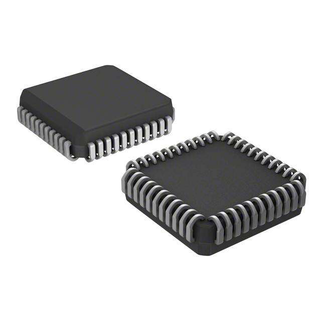
CY7C1380D CY7C1380F CY7C1382D Ordering Information The below table lists the key package features and ordering codes. The table contains only the parts that are currently available. If you do not see what you are looking for, contact your local sales representative. For more information, visit the Cypress website at www.cypress.com and refer to the product summary page at http://www.cypress.com/products. Speed MPN Package Operating Part and Package Type (MHz) Ordering Code Status Diagram Range 250 CY7C1380D-250AXC [37] NRND 51-85050 100-pin TQFP (14 × 20 × 1.4 mm) Pb-free Commercial 200 CY7C1380D-200AXC [37] 51-85050 100-pin TQFP (14 × 20 × 1.4 mm) Pb-free Commercial CY7C1382D-200AXC [37] 167 CY7C1380D-167AXC [37] 51-85050 100-pin TQFP (14 × 20 × 1.4 mm) Pb-free Commercial CY7C1382D-167AXC [37] . s CY7C1380D-167AXI [37] 51-85050 100-pin TQFP (14 × 20 × 1.4 mm) Pb-free Industrial n CY7C1380F-167BZI [37] 51-85180 165-ball FBGA (13 × 15 × 1.4 mm) g i s Ordering Code Definitions e D CY 7 C 138X X - XXX XX X X w e Temperature Range: X = C or I N C = Commercial; I = Industrial r Pb-free o Package Type: XX = A or BZ f A = 100-pin TQFP d BZ = 165-ball FPBGA e d Frequency Range: XXX = 250 MHz or 200 MHz or 167 MHz n Die Revision: X = D or F e D 90 nm m F 90nm errata fix PCN084636 m Part Identifier: 138X = 1380 or 1382 o 1380 = SCD, 512 K × 36 (18 Mb) c 1382 = SCD, 1 Mb × 18 (18 Mb) e Technology Code: C = CMOS R Marketing Code: 7 = SRAM t o Company ID: CY = Cypress N Note 37.These MPNs are not recommended for new designs. Document Number: 38-05543 Rev. *S Page 28 of 38
CY7C1380D CY7C1380F CY7C1382D Package Diagrams Figure 9. 100-pin TQFP (14 × 20 × 1.4 mm) A100RA Package Outline, 51-85050 . s n g i s e D w e N r o f d e d n e 51-85050 *E m m o c e R t o N Document Number: 38-05543 Rev. *S Page 29 of 38
CY7C1380D CY7C1380F CY7C1382D Package Diagrams (continued) Figure 10. 165-ball FBGA (13 × 15 × 1.4 mm) BB165D/BW165D (0.5 Ball Diameter) Package Outline, 51-85180 . s n g i s e D w e N r o f d e d n e m m o c e 51-85180 *G R t o N Document Number: 38-05543 Rev. *S Page 30 of 38
CY7C1380D CY7C1380F CY7C1382D Acronyms Document Conventions Units of Measure Acronym Description CMOS Complementary Metal Oxide Semiconductor Symbol Unit of Measure FBGA Fine-Pitch Ball Grid Array °C degree Celsius I/O Input/Output MHz megahertz JTAG Joint Test Action Group µA microampere mA milliampere LSB Least Significant Bit mm millimeter MSB Most Significant Bit ms millisecond OE Output Enable ns nanosecond SRAM Static Random Access Memory . ohm s TCK Test Clock n % percent TMS Test Mode Select g pF picofarad i s TDI Test Data-In V volt e TDO Test Data-Out D W watt TQFP Thin Quad Flat Pack w TTL Transistor-Transistor Logic e N r o f d e d n e m m o c e R t o N Document Number: 38-05543 Rev. *S Page 31 of 38
CY7C1380D CY7C1380F CY7C1382D Errata This section describes the Ram9 Sync ZZ pin and JTAG issues. Details include trigger conditions, the devices affected, proposed workaround and silicon revision applicability. Please contact your local Cypress sales representative if you have further questions. Part Numbers Affected Density & Revision Package Type Operating Range 18Mb-Ram9 Synchronous SRAMs: CY7C138*D, CY7C138*F 100-pin TQFP Commercial/ Industrial 165-ball FBGA Industrial Product Status . All of the devices in the Ram9 18Mb Sync family are qualified and available in production quantities. s n Ram9 Sync ZZ Pin & JTAG Issues Errata Summary g i The following table defines the errata applicable to available Ram9 18Mb Sync family devices. s e D Item Issues Description Device Fix Status w 1. ZZ Pin When asserted HIGH, the ZZ pin places 18M-Ram9 (90 nm) For the 18M Ram9 (90 nm) device in a “sleep” condition with data integrity devices, there is no plan to fix e preserved.The ZZ pin currently does not have this issue. N an internal pull-down resistor and hence cannot be left floating externally by the user r o during normal mode of operation. f 2. JTAG During JTAG test mode, the Boundary scan 18M-Ram9 (90 nm) This issue will be fixed in the d Functionality circuitry does not perform as described in the new revision, which use the e datasheet.However, it is possible to perform 65nm technology. Please d the JTAG test with these devices in “BYPASS contact your local sales rep for n mode”. availability. e m m o c e R t o N Document Number: 38-05543 Rev. *S Page 32 of 38
CY7C1380D CY7C1380F CY7C1382D 1. ZZ Pin Issue ■ PROBLEM DEFINITION The problem occurs only when the device is operated in the normal mode with ZZ pin left floating. The ZZ pin on the SRAM device does not have an internal pull-down resistor. Switching noise in the system may cause the SRAM to recognize a HIGH on the ZZ input, which may cause the SRAM to enter sleep mode. This could result in incorrect or undesirable operation of the SRAM. ■ TRIGGER CONDITIONS Device operated with ZZ pin left floating. ■ SCOPE OF IMPACT When the ZZ pin is left floating, the device delivers incorrect data. ■ WORKAROUND . Tie the ZZ pin externally to ground. s n g ■ FIX STATUS i For the 18M Ram9 (90 nm) devices, there is no plan to fix this issue. s e D 2. JTAG Functionality ■ PROBLEM DEFINITION w The problem occurs only when the device is operated in the JTAG test mode.During this mode, the JTAG circuitry can perform e incorrectly by delivering the incorrect data or the incorrect scan chain length. N ■ TRIGGER CONDITIONS r o Several conditions can trigger this failure mode. f 1. The device can deliver an incorrect length scan chain when operating in JTAG mode. d 2. Some Byte Write inputs only recognize a logic HIGH level when in JTAG mode. e 3. Incorrect JTAG data can be read from the device when the ZZ input is tied HIGH during JTAG operation. d n e ■ SCOPE OF IMPACT m The device fails for JTAG test. This does not impact the normal functionality of the device. m ■ WORKAROUND o 1.Perform JTAG testing with these devices in “BYPASS mode”. c 2.Do not use JTAG test. e R ■ FIX STATUS t This issue will be fixed in the new revision, which use the 65nm technology. Please contact your local sales rep for availability. o N Document Number: 38-05543 Rev. *S Page 33 of 38
CY7C1380D CY7C1380F CY7C1382D Document History Page Document Title: CY7C1380D/CY7C1380F/CY7C1382D, 18-Mbit (512K × 36/1M × 18) Pipelined SRAM Document Number: 38-05543 Submission Orig. of Rev. ECN No. Description of Change Date Change ** 254515 See ECN RKF New data sheet. *A 288531 See ECN SYT Updated Selection Guide (Removed 225 MHz and 133 MHz frequencies related information). Updated IEEE 1149.1 Serial Boundary Scan (JTAG [13]) (Edited description for non-compliance with 1149.1). Updated Electrical Characteristics (Removed 225 MHz and 133 MHz frequencies related information). . Updated Switching Characteristics (Removed 225 MHz and 133 MHz s frequencies related information). n Updated Ordering Information (Added Pb-free information for 100-pin TQFP, g 119-ball BGA and 165-ball FBGA packages) and added comment for ‘Pb-free si BG packages availability’ below the Ordering Information. e D *B 326078 See ECN PCI Updated Pin Configurations (Address expansion pins/balls in the pinouts for all packages are modified as per JEDEC standard). w Updated IEEE 1149.1 Serial Boundary Scan (JTAG [13]) (Updated TAP Instruction Set (Updated OVERVIEW (description), updated EXTEST e (description), added EXTEST Output Bus Tri-State)). N Updated Identification Register Definitions (Splitted Device Width (23:18) into r two rows (one for 119-ball BGA and another for 165-ball FBGA), retained the o same values of 165-ball FBGA and changed the values from 000000 to 101000 f for 119-ball BGA) d Updated Electrical Characteristics (Modified Test Conditions for VOL, VOH e parameters). d Updated Thermal Resistance (Changed JA and JC for 100-pin TQFP n Package from 31 and 6 C/W to 28.66 and 4.08 C/W respectively, changed e JA and JC for 119-ball BGA Package from 45 and 7 C/W to 23.8 and m 6.2C/W respectively, changed and for 165-ball FBGA Packagefrom JA JC m 46 and 3 C/W to 20.7 and 4.0 C/W respectively). Updated Ordering Information (Updated part numbers) and removed comment o of ‘Pb-free BG packages availability’ below the Ordering Information. c e *C 416321 See ECN NXR Changed status from Preliminary to Final. R Changed address of Cypress Semiconductor Corporation from “3901 North First Street” to “198 Champion Court”. t Updated Electrical Characteristics (Changed the description of I parameter o X from Input Load Current to Input Leakage Current, changed the minimum and N maximum values of I parameter (corresponding to Input Current of MODE) X from –5 A and 30 A to –30 A and 5 A, changed the minimum and maximum values of I parameter (corresponding to Input current of ZZ) from –30 A and X 5 A to –5 A and 30 A, updated Note 21). Updated Ordering Information (Updated part numbers) and replaced Package Name column with Package Diagram in the Ordering Information table. *D 475009 See ECN VKN Updated TAP AC Switching Characteristics (Changed minimum values of t , TH and t parameters from 25 ns to 20 ns, and maximum value of t TL TDOV parameter from 5 ns to 10 ns). Updated Maximum Ratings (Added the Maximum Rating for Supply Voltage on V Relative to GND). DDQ Updated Ordering Information (Updated part numbers). *E 776456 See ECN VKN Updated Features (Included CY7C1380F/CY7C1382F related information). Updated Functional Description (Included CY7C1380F/CY7C1382F related information). Document Number: 38-05543 Rev. *S Page 34 of 38
CY7C1380D CY7C1380F CY7C1382D Document History Page (continued) Document Title: CY7C1380D/CY7C1380F/CY7C1382D, 18-Mbit (512K × 36/1M × 18) Pipelined SRAM Document Number: 38-05543 Submission Orig. of Rev. ECN No. Description of Change Date Change *E (cont.) 776456 See ECN VKN Updated Logic Block Diagram – CY7C1380D/CY7C1380F (Included CY7C1380F related information, added the Note “CY7C1380F and CY7C1382F in 119-ball BGA package have only 1 chip enable (CE ).” and 1 referred the same note in the title). Updated Logic Block Diagram – CY7C1382D/CY7C1382F (Included CY7C1382F related information, added the Note “CY7C1380F and CY7C1382F in 119-ball BGA package have only 1 chip enable (CE ).” and 1 referred the same note in the title). Updated Pin Configurations (Included CY7C1380F/CY7C1382F related . information). s n Updated Functional Overview (Included CY7C1380F/CY7C1382F related g information). i Updated Truth Table (Included CY7C1380F/CY7C1382F related information). s Updated Truth Table for Read/Write (Included CY7C1380F related e information). D Updated Truth Table for Read/Write (Included CY7C1382F related information). w Updated IEEE 1149.1 Serial Boundary Scan (JTAG [13]) (Included e CY7C1380F/CY7C1382F related information). N Updated Identification Register Definitions (Included CY7C1380F/CY7C1382F related information). r o Updated Ordering Information (Updated part numbers). f *F 2648065 01/27/09 VKN / Updated Ordering Information (To include CY7C1380F/CY7C1382F in 100-pin d PYRS TSOP package and 165-ball FBGA package) and modified text on top of the e Ordering information table. d n *G 2897120 03/22/2010 NJY Updated Ordering Information (Removed inactive parts). e Updated Package Diagrams. m *H 3067398 10/20/10 NJY Updated Ordering Information (The part CY7C1380F-167BGC is found to be in “EOL-Prune” state in Oracle PLM and therefore, it has been removed) and m added Ordering Code Definitions. o *I 3159479 02/01/2011 NJY Added Acronyms and Units of Measure. c Updated Package Diagrams. e Minor edits. R Updated to new template. t o *J 3192403 03/10/2011 NJY Updated to new template. N *K 3210400 03/30/11 NJY Updated Ordering Information (Removed pruned part CY7C1380D-167BZC from the ordering information table). *L 3575733 04/09/2012 NJY / PRIT Updated Features (Removed CY7C1382F related information, removed 165-ball FBGA package related information for CY7C1382D, removed 100-pin TQFP package related information for CY7C1380F, removed 119-ball BGA package related information). Updated Functional Description (Removed the Note “For best practices or recommendations, please refer to the Cypress application note AN1064, SRAM System Design Guidelines on www.cypress.com.” and its reference, removed the Note “CE CE are for 100-pin TQFP and 165-ball FBGA 3, 2 packages only. 119-ball BGA is offered only in 1 chip enable.” and its reference). Updated Logic Block Diagram – CY7C1380D/CY7C1380F (Removed the Note “CY7C1380F and CY7C1382F in 119-ball BGA package have only 1 chip enable (CE ).” and its reference). 1 Updated Logic Block Diagram – CY7C1382D (Removed CY7C1382F related information, removed the Note “CY7C1380F and CY7C1382F in 119-ball BGA package have only 1 chip enable (CE ).” and its reference). 1 Document Number: 38-05543 Rev. *S Page 35 of 38
CY7C1380D CY7C1380F CY7C1382D Document History Page (continued) Document Title: CY7C1380D/CY7C1380F/CY7C1382D, 18-Mbit (512K × 36/1M × 18) Pipelined SRAM Document Number: 38-05543 Submission Orig. of Rev. ECN No. Description of Change Date Change *L (cont.) 3575733 04/09/2012 NJY / PRIT Updated Pin Configurations (Removed CY7C1382F related information, removed 119-ball BGA package related information, removed 100-pin TQFP package related information for CY7C1380F, removed 165-ball FBGA package related information for CY7C1382D, removed the Note “CE CE are 3, 2 for 100-pin TQFP and 165-ball FBGA packages only. 119-ball BGA is offered only in 1 chip enable.” and its reference). Updated Functional Overview (Removed CY7C1382F related information). Updated Truth Table (Removed CY7C1382F related information). Updated Truth Table for Read/Write (Removed CY7C1382F related . information). s n Updated IEEE 1149.1 Serial Boundary Scan (JTAG [13]) (Removed g CY7C1380D, CY7C1382D, and CY7C1382F related information). i Updated Identification Register Definitions (Removed CY7C1380D, s CY7C1382D, and CY7C1382F related information, removed 119-ball BGA e package related information). D Updated Scan Register Sizes (Removed 119-ball BGA package related information). w Removed Boundary Scan Order (Corresponding to 119-ball BGA). e Updated Capacitance (Removed 119-ball BGA package related information). N Updated Thermal Resistance (Removed 119-ball BGA package related information). r o Updated Package Diagrams (Removed 119-ball BGA package related f information). d *M 3945784 03/27/2013 PRIT Updated Package Diagrams: e spec 51-85180 – Changed revision from *E to *F. d n *N 3977530 04/23/2013 PRIT Added Errata. e *O 4068739 07/20/2013 PRIT Added Errata footnotes (Note 1, 2, 3, 4, 5, 13). m Updated Pin Configurations: Added Note 1 and referred the same note in Figure1. m Added Note 2, 3 and referred the same note in Figure2. o Updated Pin Definitions: c Added Note 4 and referred the same note in ZZ pin. e Added Note 5 and referred the same note in TDO, TDI, TMS, TCK pins. R Updated IEEE 1149.1 Serial Boundary Scan (JTAG [13]): Added Note 13 and referred the same note in JTAG in the heading. t o Updated Errata. N Updated to new template. *P 4150971 10/08/2013 PRIT Updated Errata. *Q 4569232 11/14/2014 PRIT Updated Functional Description: Added “For a complete list of related documentation, click here.” at the end. Updated Package Diagrams: spec 51-85050 – Changed revision from *D to *E. *R 4739641 04/24/2015 PRIT Updated to new template. Completing Sunset Review. Document Number: 38-05543 Rev. *S Page 36 of 38
CY7C1380D CY7C1380F CY7C1382D Document History Page (continued) Document Title: CY7C1380D/CY7C1380F/CY7C1382D, 18-Mbit (512K × 36/1M × 18) Pipelined SRAM Document Number: 38-05543 Submission Orig. of Rev. ECN No. Description of Change Date Change *S 5190429 03/29/2016 PRIT Added watermark “Not Recommended for New Designs.” across the document. Updated Ordering Information: No change in part numbers. Added a column “MPN Status”. Added Note 37 and referred the same note in all MPNs. Updated Package Diagrams: spec 51-85180 – Changed revision from *F to *G. Updated to new template. . Completing Sunset Review. s n g i s e D w e N r o f d e d n e m m o c e R t o N Document Number: 38-05543 Rev. *S Page 37 of 38
CY7C1380D CY7C1380F CY7C1382D Sales, Solutions, and Legal Information Worldwide Sales and Design Support Cypress maintains a worldwide network of offices, solution centers, manufacturer’s representatives, and distributors. To find the office closest to you, visit us at Cypress Locations. Products PSoC® Solutions ARM® Cortex® Microcontrollers cypress.com/arm cypress.com/psoc Automotive cypress.com/automotive PSoC 1 | PSoC 3 | PSoC 4 | PSoC 5LP Clocks & Buffers cypress.com/clocks Cypress Developer Community Interface cypress.com/interface Community | Forums | Blogs | Video | Training Lighting & Power Control cypress.com/powerpsoc Technical Support Memory cypress.com/memory . s cypress.com/support PSoC cypress.com/psoc n g Touch Sensing cypress.com/touch i s USB Controllers cypress.com/usb e Wireless/RF cypress.com/wireless D w e N r o f d e d n e m m o c e R t o © Cypress Semiconductor Corporation 2004-2016. This document is the property of Cypress Semiconductor Corporation and its subsidiaries, including Spansion LLC ("Cypress"). This document, including any software or firmware included or referenced in this document ("Software"), is owned by Cypress under the intellectual property laws and treaties of the United States and other countries N worldwide. Cypress reserves all rights under such laws and treaties and does not, except as specifically stated in this paragraph, grant any license under its patents, copyrights, trademarks, or other intellectual property rights. If the Software is not accompanied by a license agreement and you do not otherwise have a written agreement with Cypress governing the use of the Software, then Cypress hereby grants you under its copyright rights in the Software, a personal, non-exclusive, nontransferable license (without the right to sublicense) (a) for Software provided in source code form, to modify and reproduce the Software solely for use with Cypress hardware products, only internally within your organization, and (b) to distribute the Software in binary code form externally to end users (either directly or indirectly through resellers and distributors), solely for use on Cypress hardware product units. Cypress also grants you a personal, non-exclusive, nontransferable, license (without the right to sublicense) under those claims of Cypress's patents that are infringed by the Software (as provided by Cypress, unmodified) to make, use, distribute, and import the Software solely to the minimum extent that is necessary for you to exercise your rights under the copyright license granted in the previous sentence. Any other use, reproduction, modification, translation, or compilation of the Software is prohibited. CYPRESS MAKES NO WARRANTY OF ANY KIND, EXPRESS OR IMPLIED, WITH REGARD TO THIS DOCUMENT OR ANY SOFTWARE, INCLUDING, BUT NOT LIMITED TO, THE IMPLIED WARRANTIES OF MERCHANTABILITY AND FITNESS FOR A PARTICULAR PURPOSE. Cypress reserves the right to make changes to this document without further notice. Cypress does not assume any liability arising out of the application or use of any product or circuit described in this document. Any information provided in this document, including any sample design information or programming code, is provided only for reference purposes. It is the responsibility of the user of this document to properly design, program, and test the functionality and safety of any application made of this information and any resulting product. Cypress products are not designed, intended, or authorized for use as critical components in systems designed or intended for the operation of weapons, weapons systems, nuclear installations, life-support devices or systems, other medical devices or systems (including resuscitation equipment and surgical implants), pollution control or hazardous substances management, or other uses where the failure of the device or system could cause personal injury, death, or property damage ("Unintended Uses"). A critical component is any component of a device or system whose failure to perform can be reasonably expected to cause the failure of the device or system, or to affect its safety or effectiveness. Cypress is not liable, in whole or in part, and Company shall and hereby does release Cypress from any claim, damage, or other liability arising from or related to all Unintended Uses of Cypress products. Company shall indemnify and hold Cypress harmless from and against all claims, costs, damages, and other liabilities, including claims for personal injury or death, arising from or related to any Unintended Uses of Cypress products. Cypress, the Cypress logo, Spansion, the Spansion logo, and combinations thereof, PSoC, CapSense, EZ-USB, F-RAM, and Traveo are trademarks or registered trademarks of Cypress in the United States and other countries. For a more complete list of Cypress trademarks, visit cypress.com. Other names and brands may be claimed as property of their respective owners. Document Number: 38-05543 Rev. *S Revised March 29, 2016 Page 38 of 38 i486 is a trademark, and Intel and Pentium are registered trademarks of Intel Corporation. PowerPC is a trademark of IBM Corporation.