 Datasheet下载
- 型号: AS4C128M16D3-12BIN
- 制造商: ALLIANCE MEMORY INC
- 库位|库存: xxxx|xxxx
- 要求:
| 数量阶梯 | 香港交货 | 国内含税 |
| +xxxx | $xxxx | ¥xxxx |
查看当月历史价格
查看今年历史价格
AS4C128M16D3-12BIN产品简介:
ICGOO电子元器件商城为您提供AS4C128M16D3-12BIN由ALLIANCE MEMORY INC设计生产,在icgoo商城现货销售,并且可以通过原厂、代理商等渠道进行代购。 AS4C128M16D3-12BIN价格参考。ALLIANCE MEMORY INCAS4C128M16D3-12BIN封装/规格:存储器, SDRAM - DDR3 存储器 IC 2Gb (128M x 16) 并联 800MHz 20ns 96-FBGA(13x9)。您可以下载AS4C128M16D3-12BIN参考资料、Datasheet数据手册功能说明书,资料中有AS4C128M16D3-12BIN 详细功能的应用电路图电压和使用方法及教程。
Alliance Memory, Inc. 是一家专注于提供高性能存储解决方案的公司,其产品广泛应用于多个行业领域。型号为 AS4C128M16D3-12BIN 的存储器是一款 DRAM(动态随机存取存储器)芯片,具有较大的存储容量和较高的数据访问速度,适用于对性能和稳定性有较高要求的应用场景。

该芯片的主要应用场景包括:

1. 工业控制设备:如PLC(可编程逻辑控制器)、工控机等,用于实时数据处理与存储,保障设备高效稳定运行。

2. 通信设备:用于路由器、交换机、基站等通信基础设施中,作为临时数据缓存,提升数据传输与处理效率。

3. 网络设备:支持高速数据包处理和缓存,适用于高性能网络设备中,如防火墙、服务器适配器等。

4. 医疗设备:如影像设备、监护仪等,用于快速处理和存储大量医疗数据,确保设备响应迅速、数据准确。

5. 汽车电子系统:在车载信息娱乐系统(IVI)、高级驾驶辅助系统(ADAS)中,用于图像和数据的高速缓存与处理。

6. 消费类电子产品:如高端平板电脑、智能电视等,用于提升系统运行速度和多任务处理能力。

该芯片采用 128M x16 的组织结构,支持 DDR3 SDRAM 技术,具备高速传输、低功耗等优点,适合需要高性能内存支持的嵌入式系统和持续运行的工业环境。
| 参数 | 数值 |
| 产品目录 | 集成电路 (IC)半导体 |
| 描述 | IC SDRAM DDR3 128M X 16 96-FBGA动态随机存取存储器 2G, 1.5V, 1600Mhz 128M x 16 DDR3 |
| 产品分类 | |
| 品牌 | Alliance MemoryAlliance Memory, Inc. |
| 产品手册 | |
| 产品图片 | |
| rohs | 符合RoHS无铅 / 符合限制有害物质指令(RoHS)规范要求 |
| 产品系列 | 内存,动态随机存取存储器,Alliance Memory AS4C128M16D3-12BIN- |
| 数据手册 | |
| 产品型号 | AS4C128M16D3-12BINAS4C128M16D3-12BIN |
| 产品种类 | 动态随机存取存储器 |
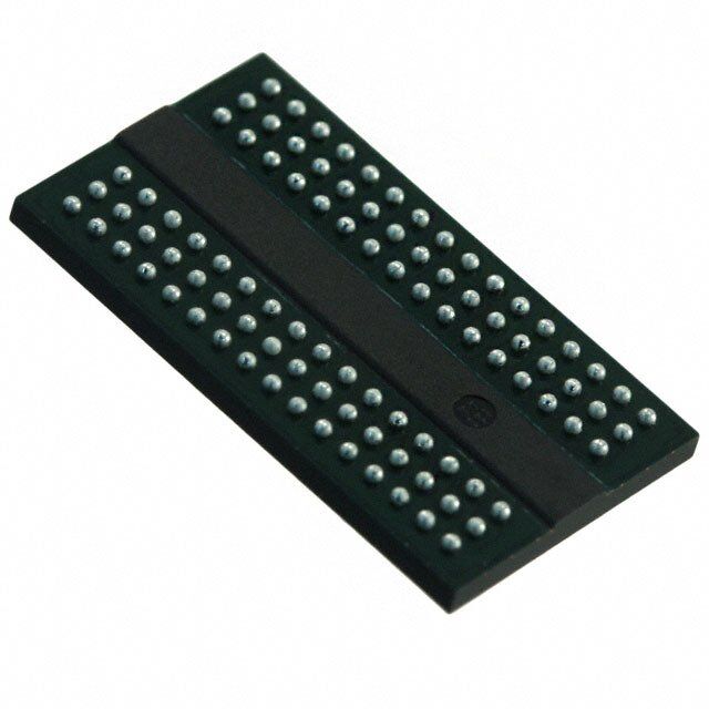
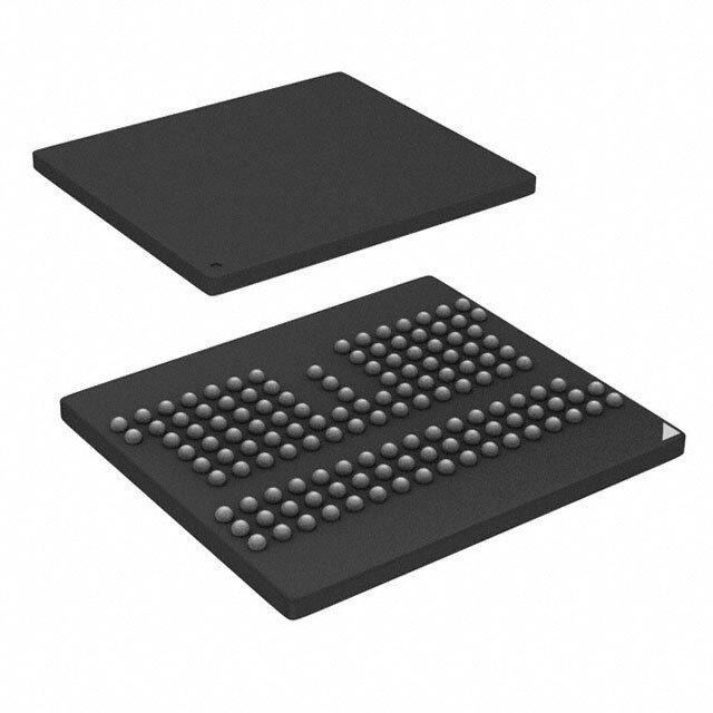
| 供应商器件封装 | 96-FBGA (13x9) |
| 其它名称 | 1450-1084 |
| 包装 | 托盘 |
| 商标 | Alliance Memory |
| 存储器类型 | DDR3 SDRAM |
| 存储容量 | 256 MB2G(128M x 16) |
| 安装风格 | SMD/SMT |
| 封装 | Tray |
| 封装/外壳 | 96-TFBGA |
| 封装/箱体 | TFBGA |
| 工作温度 | -40°C ~ 85°C |
| 工厂包装数量 | 190 |
| 接口 | 并联 |
| 数据总线宽度 | 16 bit |
| 最大工作温度 | + 85 C |
| 最大时钟频率 | 1600 MHz |
| 最小工作温度 | - 40 C |
| 标准包装 | 190 |
| 格式-存储器 | RAM |
| 电压-电源 | 1.425 V ~ 1.575 V |
| 电源电压-最大 | 1.5 V |
| 电源电压-最小 | 1.5 V |
| 类型 | DDR3 |
| 系列 | AS4C128M16D3 |
| 组织 | 128 M x 16 |
| 访问时间 | 12 ns |
| 速度 | 800MHz |


- 商务部:美国ITC正式对集成电路等产品启动337调查
- 曝三星4nm工艺存在良率问题 高通将骁龙8 Gen1或转产台积电
- 太阳诱电将投资9.5亿元在常州建新厂生产MLCC 预计2023年完工
- 英特尔发布欧洲新工厂建设计划 深化IDM 2.0 战略
- 台积电先进制程称霸业界 有大客户加持明年业绩稳了
- 达到5530亿美元!SIA预计今年全球半导体销售额将创下新高
- 英特尔拟将自动驾驶子公司Mobileye上市 估值或超500亿美元
- 三星加码芯片和SET,合并消费电子和移动部门,撤换高东真等 CEO
- 三星电子宣布重大人事变动 还合并消费电子和移动部门
- 海关总署:前11个月进口集成电路产品价值2.52万亿元 增长14.8%

_renders/IS42S32800D-6BLI.jpg)


PDF Datasheet 数据手册内容提取
AS4C128M16D3 REVISION HISTORY AS4C128M16D3 – 96-ball FBGA PACKAGE Revision Description Issue Date Rev. 1.0 Initial Issue February 2014 Rev. 2.0 Typing error – in Table 2 page 2 – incorrect temperature range June 2014 amended to: - Commercial (Extended) (0 ~ 95°C) - Industrial (-40 ~ 95°C) Rev 3.0 Updated Table 11. Recommended DC Operating Conditions – page 21 August 2014 Added CL=5 & CL=6 to Table 18 – page 26 Confidential 1 Rev. 3.0 Aug. /2014
AS4C128M16D3 2Gb (128M x 16 bit) DDR3 Synchronous DRAM (SDRAM) Confidential Advanced (Rev. 3.0, Aug. /2014) Features Overview JEDEC Standard Compliant The 2Gb Double-Data-Rate-3 DRAMs is double data Power supplies: VDD & VDDQ = +1.5V 0.075V rate architecture to achieve high-speed operation. It is internally configured as an eight bank DRAM. Operating temperature: The 2Gb chip is organized as 16Mbit x 16 I/Os x 8 - Commercial (0 ~ 95°C) bank devices. These synchronous devices achieve high - Industrial (-40 ~ 95°C) speed double-data-rate transfer rates of up to 1600 Supports JEDEC clock jitter specification Mb/sec/pin for general applications. Fully synchronous operation The chip is designed to comply with all key DDR3 Fast clock rate: 800MHz DRAM key features and all of the control and address Differential Clock, CK & CK# inputs are synchronized with a pair of externally Bidirectional differential data strobe supplied differential clocks. Inputs are latched at the - DQS & DQS# cross point of differential clocks (CK rising and CK# 8 internal banks for concurrent operation falling). All I/Os are synchronized with differential DQS pair in a source synchronous fashion. 8n-bit prefetch architecture These devices operate with a single 1.5V ± 0.075V Internal pipeline architecture power supply and are available in BGA packages. Precharge & active power down Programmable Mode & Extended Mode registers Additive Latency (AL): 0, CL-1, CL-2 Programmable Burst lengths: 4, 8 Burst type: Sequential / Interleave Output Driver Impedance Control 8192 refresh cycles / 64ms - Average refresh period 7.8μs @ -40℃ ≦TC≦ +85℃ 3.9μs @ +85℃ <TC≦ +95℃ Write Leveling OCD Calibration Dynamic ODT (Rtt_Nom & Rtt_WR) RoHS compliant Auto Refresh and Self Refresh 96-ball 9 x 13 x 1.2mm FBGA package - All parts are ROHS Compliant Table 1. Speed Grade Information Speed Grade Clock Frequency CAS Latency t (ns) t (ns) RCD RP DDR3-1600 800 MHz 11 13.75 13.75 Table 2 – Ordering Information for ROHS Compliant Products Product part No Org Temperature Package AS4C128M16D3-12BCN 128M x 16 Commercial(Extended) 96-ball 0°C to 95°C FBGA AS4C128M16D3-12BIN 128M x 16 Industrial 96-ball -40°C to 95°C FBGA Confidential 2 Rev. 3.0 Aug. /2014
AS4C128M16D3 Figure 1. Ball Assignment (FBGA Top View) 1 2 3 … 7 8 9 A VDDQ DQ13 DQ15 DQ12 VDDQ VSS B VSSQ VDD VSS UDQS# DQ14 VSSQ . C VDDQ DQ11 DQ9 UDQS DQ10 VDDQ D VSSQ VDDQ UDM DQ8 VSSQ VDD E VSS VSSQ DQ0 LDM VSSQ VDDQ F VDDQ DQ2 LDQS DQ1 DQ3 VSSQ G VSSQ DQ6 LDQS# VDD VSS VSSQ H VREFDQ VDDQ DQ4 DQ7 DQ5 VDDQ J NC VSS RAS# CK VSS NC K ODT VDD CAS# CK# VDD CKE L NC CS# WE# A10/AP ZQ NC M VSS BA0 BA2 NC VREFCA VSS N VDD A3 A0 A12/BC # BA1 VDD P VSS A5 A2 A1 A4 VSS R VDD A7 A9 A11 A6 VDD T VSS RESET# A13 NC A8 VSS Confidential 3 Rev. 3.0 Aug. /2014
AS4C128M16D3 Figure 2. Block Diagram CK DLL CK# BCULFOFCEKR ow oder CE1L6LM A xR 1R6AY CKE Rec (BANK #0) D Column Decoder RESET# CONTROL ow oder CE1L6LM A xR 1R6AY CS# SIGNAL Rec (BANK #1) D RAS# COMMAND GENERATOR Column Decoder CAS# DECODER WE# ow oder CE1L6LM A xR 1R6AY Rec (BANK #2) D Column Decoder A10/AP A12/BC# COLUMN COUNTER REMGOISDTEER ow oder CE1L6LM A xR 1R6AY Rec (BANK #3) D Column Decoder A0~A9 A11 ADDRESS BAA130 BUFFER Row ecoder CE(B1L6ALMN A KxR 1#R64A)Y D BA1 Column Decoder BA2 ZQCL ZQ REFRESH ZQCS CAL ow oder CE1L6LM A xR 1R6AY COUNTER Rec (BANK #5) D Column Decoder RZQ VSSQ LDQS DATA ow oder CE1L6LM A xR 1R6AY LDQS# Rec (BANK #6) STROBE D UDQS DQ Column Decoder BUFFER Buffer UDQS# DQ0 ~ DQ15 ow oder CE1L6LM A xR 1R6AY Rec (BANK #7) D Column Decoder ODT LDM UDM Confidential 4 Rev. 3.0 Aug. /2014
AS4C128M16D3 Figure 3. State Diagram This simplified State Diagram is intended to provide an overview of the possible state transitions and the commands to control them. In particular, situations involving more than one bank, the enabling or disabling of on-die termination and some other events are not captured in full detail Power applied Power Reset MRS,MPR, Self Initialization Write On Procedure Refresh Leveling E from any RESET ZQCL MRS SR RX state S ZQCL,ZQCS ZQ Idle REF Refreshing Calibration P ACT P DE D X ACT = Active Active Precharge Power Activating Power PRE = Precharge Down Down PREA = Precharge All P MRS = Mode Register Set DX P REF = Refresh DE RESET = Start RESET Procedure Bank Read = RD, RDS4, RDS8 Activating Read A = RDA, RDAS4, RDAS8 Write = WR, WRS4, WRS8 WRITE WRITE RITE A READ READ Write A = WRA, WRAS4, WRAS8 W ZQCL = ZQ Calibration Long Writing READ Reading ZQCS = ZQ Calibration Short WRITE PDE = Enter Power-down R E A D A PDX = Exit Power-down SRE = Self-Refresh entry WRITE A READ A SRX = Self-Refresh exit MPR = Multi-Purpose Register W RIT E A READ A P Writing R E P PR , P ER Reading E, PR REA ERP , Automatic Sequence EA A Command Sequence Precharging Confidential 5 Rev. 3.0 Aug. /2014
AS4C128M16D3 Ball Descriptions Table 2. Ball Descriptions Symbol Type Description CK, CK# Input Differential Clock: CK and CK# are driven by the system clock. All SDRAM input signals are sampled on the crossing of positive edge of CK and negative edge of CK#. Output (Read) data is referenced to the crossings of CK and CK# (both directions of crossing). CKE Input Clock Enable: CKE activates (HIGH) and deactivates (LOW) the CK signal. If CKE goes LOW synchronously with clock, the internal clock is suspended from the next clock cycle and the state of output and burst address is frozen as long as the CKE remains LOW. When all banks are in the idle state, deactivating the clock controls the entry to the Power Down and Self Refresh modes. BA0-BA2 Input Bank Address: BA0-BA2 define to which bank the BankActivate, Read, Write, or BankPrecharge command is being applied. A0-A13 Input Address Inputs: A0-A13 are sampled during the BankActivate command (row address A0-A13) and Read/Write command (column address A0-A9 with A10 defining Auto Precharge). A10/AP Input Auto-Precharge: A10 is sampled during Read/Write commands to determine whether Autoprecharge should be performed to the accessed bank after the Read/Write operation. (HIGH: Autoprecharge; LOW: no Autoprecharge). A10 is sampled during a Precharge command to determine whether the Precharge applies to one bank (A10 LOW) or all banks (A10 HIGH). A12/BC# Input Burst Chop: A12/BC# is sampled during Read and Write commands to determine if burst chop (on the fly) will be performed. (HIGH - no burst chop; LOW - burst chopped). CS# Input Chip Select: CS# enables (sampled LOW) and disables (sampled HIGH) the command decoder. All commands are masked when CS# is sampled HIGH. It is considered part of the command code. RAS# Input Row Address Strobe: The RAS# signal defines the operation commands in conjunction with the CAS# and WE# signals and is latched at the crossing of positive edges of CK and negative edge of CK#. When RAS# and CS# are asserted "LOW" and CAS# is asserted "HIGH," either the BankActivate command or the Precharge command is selected by the WE# signal. When the WE# is asserted "HIGH," the BankActivate command is selected and the bank designated by BA is turned on to the active state. When the WE# is asserted "LOW," the Precharge command is selected and the bank designated by BA is switched to the idle state after the precharge operation. CAS# Input Column Address Strobe: The CAS# signal defines the operation commands in conjunction with the RAS# and WE# signals and is latched at the crossing of positive edges of CK and negative edge of CK#. When RAS# is held "HIGH" and CS# is asserted "LOW," the column access is started by asserting CAS# "LOW." Then, the Read or Write command is selected by asserting WE# “HIGH " or “LOW". WE# Input Write Enable: The WE# signal defines the operation commands in conjunction with the RAS# and CAS# signals and is latched at the crossing of positive edges of CK and negative edge of CK#. The WE# input is used to select the BankActivate or Precharge command and Read or Write command. LDQS, Input / Bidirectional Data Strobe: Specifies timing for Input and Output data. Read Data Strobe is edge triggered. Write Data Strobe provides a setup and hold time for data and DQM. LDQS# Output LDQS is for DQ0~7, UDQS is for DQ8~15. The data strobes LDOS and UDQS are paired UDQS with LDQS# and UDQS# to provide differential pair signaling to the system during both reads and writes. UDQS# Confidential 6 Rev. 3.0 Aug. /2014
AS4C128M16D3 LDM, Input Data Input Mask: Input data is masked when DM is sampled HIGH during a write cycle. LDM masks DQ0-DQ7, UDM masks DQ8-DQ15. UDM DQ0 - DQ15 Input / Data I/O: The data bus input and output data are synchronized with positive and negative Output edges of DQS/DQS#. The I/Os are byte-maskable during Writes. ODT Input On Die Termination: ODT (registered HIGH) enables termination resistance internal to the DDR3 SDRAM. When enabled, ODT is applied to each DQ, DQS, DQS#. The ODT pin will be ignored if Mode-registers, MR1and MR2, are programmed to disable RTT. RESET# Input Active Low Asynchronous Reset: Reset is active when RESET# is LOW, and inactive when RESET# is HIGH. RESET# must be HIGH during normal operation. RESET# is a CMOS rail to rail signal with DC high and low at 80% and 20% of VDD VDD Supply Power Supply: +1.5V 0.075V VSS Supply Ground VDDQ Supply DQ Power: +1.5V 0.075V. VSSQ Supply DQ Ground VREFCA Supply Reference voltage for CA VREFDQ Supply Reference voltage for DQ ZQ Supply Reference pin for ZQ calibration. NC - No Connect: These pins should be left unconnected. Confidential 7 Rev. 3.0 Aug. /2014
AS4C128M16D3 Operation Mode Truth Table Table 3. Truth Table (Note (1), (2)) Command State CKEn-1(3) CKEn DM BA0-2 A10/AP A0-9, 11, 13 A12/BC# CS# RAS# CAS# WE# BankActivate Idle(4) H H X V Row address L L H H Single Bank Precharge Any H H X V L V V L L H L All Banks Precharge Any H H X V H V V L L H L Write (Fixed BL8 or BC4) Active(4) H H X V L V V L H L L Write (BC4, on the fly) Active(4) H H X V L V L L H L L Write (BL8, on the fly) Active(4) H H X V L V H L H L L Write with Autoprecharge Active(4) H H X V H V V L H L L (Fixed BL8 or BC4) Write with Autoprecharge Active(4) H H X V H V L L H L L (BC4, on the fly) Write with Autoprecharge Active(4) H H X V H V H L H L L (BL8, on the fly) Read (Fixed BL8 or BC4) Active(4) H H X V L V V L H L H Read (BC4, on the fly) Active(4) H H X V L V L L H L H Read (BL8, on the fly) Active(4) H H X V L V H L H L H Read with Autoprecharge Active(4) H H X V H V V L H L H (Fixed BL8 or BC4) Read with Autoprecharge Active(4) H H X V H V L L H L H (BC4, on the fly) Read with Autoprecharge Active(4) H H X V H V H L H L H (BL8, on the fly) (Extended) Mode Register Set Idle H H X V OP code L L L L No-Operation Any H H X V V V V L H H H Device Deselect Any H H X X X X X H X X X Burst Stop Active(5) H X X X X X X L H H L Refresh Idle H H X V V V V L L L H SelfRefresh Entry Idle H L X V V V V L L L H X X X X H X X X SelfRefresh Exit Idle L H X V V V V L H H H X X X X H X X X Power Down Mode Entry Idle H L X V V V V L H H H X X X X H X X X Power Down Mode Exit Any L H X V V V V L H H H Data Input Mask Disable Active H X L X X X X X X X X Data Input Mask Enable(6) Active H X H X X X X X X X X ZQ Calibration Long Idle H H X X H X X L H H L ZQ Calibration Short Idle H H X X L X X L H H L NOTE 1: V=Valid data, X=Don't Care, L=Low level, H=High level NOTE 2: CKEn signal is input level when commands are provided. NOTE 3: CKEn-1 signal is input level one clock cycle before the commands are provided. NOTE 4: These are states of bank designated by BA signal. NOTE 5: Device state is 4, and 8 burst operation. NOTE 6: LDM and UDM can be enabled respectively. Confidential 8 Rev. 3.0 Aug. /2014
AS4C128M16D3 Functional Description The DDR3 SDRAM is a high-speed dynamic random access memory internally configured as an eight-bank DRAM. The DDR3 SDRAM uses an 8n prefetch architecture to achieve high speed operation. The 8n Prefetch architecture is combined with an interface designed to transfer two data words per clock cycle at the I/O pins. A single read or write operation for the DDR3 SDRAM consists of a single 8n-bit wide, four clock data transfer at the internal DRAM core and two corresponding n-bit wide, one-half clock cycle data transfers at the I/O pins. Read and write operation to the DDR3 SDRAM are burst oriented, start at a selected location, and continue for a burst length of eight or a ‘chopped’ burst of four in a programmed sequence. Operation begins with the registration of an Active command, which is then followed by a Read or Write command. The address bits registered coincident with the Active command are used to select the bank and row to be activated (BA0-BA2 select the bank; A0-A13 select the row). The address bit registered coincident with the Read or Write command are used to select the starting column location for the burst operation, determine if the auto precharge command is to be issued (via A10), and select BC4 or BL8 mode ‘on the fly’ (via A12) if enabled in the mode register. Prior to normal operation, the DDR3 SDRAM must be powered up and initialized in a predefined manner. The following sections provide detailed information covering device reset and initialization, register definition, command descriptions and device operation. Figure 4. Reset and Initialization Sequence at Power-on Ramping Ta Tb Tc Td Te Tf Tg Th Ti Tj Tk CK# CK t CKSRX VDD VDDQ T=200μs T=500μs RESET# t Tmin=10ns IS CKE t DLLK t IS t t t t t t XPR MRD MRD MRD MOD ZQinit COMMAND Note 1 MRS MRS MRS MRS ZQCL Note 1 VALID BA MR2 MR3 MR1 MR0 VALID t t IS IS ODT Static LOW in case RTT_Nom is enabled at time Tg, otherwise static HIGH or LOW VALID RTT NOTE 1. From time point “Td”until “Tk”NOP or DES commands must be applied between MRS and ZQCL commands. TIME BREAK Don't Care Confidential 9 Rev. 3.0 Aug. /2014
AS4C128M16D3 Power-up and Initialization The Following sequence is required for POWER UP and Initialization 1. Apply power (RESET# is recommended to be maintained below 0.2 x VDD, all other inputs may be undefined). RESET# needs to be maintained for minimum 200us with stable power. CKE is pulled “Low” anytime before RESET# being de-asserted (min. time 10ns). The power voltage ramp time between 300mV to VDDmin must be no greater than 200ms; and during the ramp, VDD>VDDQ and (VDD-VDDQ) <0.3 Volts. - VDD and VDDQ are driven from a single power converter output, AND - The voltage levels on all pins other than VDD, VDDQ, VSS, VSSQ must be less than or equal to VDDQ and VDD on one side and must be larger than or equal to VSSQ and VSS on the other side. In addition, VTT is limited to 0.95V max once power ramp is finished, AND - Vref tracks VDDQ/2. OR - Apply VDD without any slope reversal before or at the same time as VDDQ. - Apply VDDQ without any slope reversal before or at the same time as VTT & Vref. - The voltage levels on all pins other than VDD, VDDQ, VSS, VSSQ must be less than or equal to VDDQ and VDD on one side and must be larger than or equal to VSSQ and VSS on the other side. 2. After RESET# is de-asserted, wait for another 500us until CKE become active. During this time, the DRAM will start internal state initialization; this will be done independently of external clocks. 3. Clock (CK, CK#) need to be started and stabilized for at least 10ns or 5tCK (which is larger) before CKE goes active. Since CKE is a synchronous signal, the corresponding set up time to clock (tIS) must be meeting. Also a NOP or Deselect command must be registered (with tIS set up time to clock) before CKE goes active. Once the CKE registered “High” after Reset, CKE needs to be continuously registered “High” until the initialization sequence is finished, including expiration of tDLLK and tZQinit. 4. The DDR3 DRAM will keep its on-die termination in high impedance state as long as RESET# is asserted. Further, the DRAM keeps its on-die termination in high impedance state after RESET# deassertion until CKE is registered HIGH. The ODT input signal may be in undefined state until tIS before CKE is registered HIGH. When CKE is registered HIGH, the ODT input signal may be statically held at either LOW or HIGH. If RTT_NOM is to be enabled in MR1, the ODT input signal must be statically held LOW. In all cases, the ODT input signal remains static until the power up initialization sequence is finished, including the expiration of tDLLK and tZQinit. 5. After CKE being registered high, wait minimum of Reset CKE Exit time, tXPR, before issuing the first MRS command to load mode register.(tXPR=max (tXS, 5tCK)) 6. Issue MRS command to load MR2 with all application settings. (To issue MRS command for MR2, provide “Low” to BA0 and BA2, “High” to BA1) 7. Issue MRS Command to load MR3 with all application settings. (To issue MRS command for MR3, provide “Low” to BA2, “High” to BA0 and BA1) 8. Issue MRS Command to load MR1 with all application settings and DLL enabled. (To issue “DLL Enable” command, provide “Low” to A0, “High” to BA0 and “Low” to BA1 and BA2) 9. Issue MRS Command to load MR0 with all application settings and “DLL reset”. (To issue DLL reset command provide “High” to A8 and “Low” to BA0-BA2) 10. Issue ZQCL command to starting ZQ calibration. 11. Wait for both tDLLK and tZQinit completed. 12. The DDR3 SDRAM is now ready for normal operation. Confidential 10 Rev. 3.0 Aug. /2014
AS4C128M16D3 Reset Procedure at Stable Power The following sequence is required for RESET at no power interruption initialization. 1. Asserted RESET below 0.2*VDD anytime when reset is needed (all other inputs may be undefined). RESET needs to be maintained for minimum 100ns. CKE is pulled “Low” before RESET being de-asserted (min. time 10ns). 2. Follow Power-up Initialization Sequence step 2 to 11. 3. The Reset sequence is now completed. DDR3 SDRAM is ready for normal operation. Figure 5. Reset Procedure at Power Stable Condition Ta Tb Tc Td Te Tf Tg Th Ti Tj Tk CK# CK t CKSRX VDD VDDQ T=100ns T=500μs RESET# t Tmin=10ns IS CKE t DLLK t IS t t t t t t XPR MRD MRD MRD MOD ZQinit COMMAND Note 1 MRS MRS MRS MRS ZQCL Note 1 VALID BA MR2 MR3 MR1 MR0 VALID t t IS IS ODT Static LOW in case RTT_Nom is enabled at time Tg, otherwise static HIGH or LOW VALID RTT NOTE 1. From time point “Td”until “Tk”NOP or DES commands must be applied between MRS and ZQCL commands. TIME BREAK Don't Care Confidential 11 Rev. 3.0 Aug. /2014
AS4C128M16D3 Register Definition Programming the Mode Registers For application flexibility, various functions, features, and modes are programmable in four Mode Registers, provided by the DDR3 SDRAM, as user defined variables and they must be programmed via a Mode Register Set (MRS) command. As the default values of the Mode Registers are not defined, contents of Mode Registers must be fully initialized and/or re-initialized, i.e., written, after power up and/or reset for proper operation. Also the contents of the Mode Registers can be altered by re-executing the MRS command during normal operation. When programming the mode registers, even if the user chooses to modify only a sub-set of the MRS fields, all address fields within the accessed mode register must be redefined when the MRS command is issued. MRS command and DLL Reset do not affect array contents, which mean these commands can be executed any time after power- up without affecting the array contents. The mode register set command cycle time, tMRD is required to complete the write operation to the mode register and is the minimum time required between two MRS commands shown in Figure of tMRD timing. Figure 6. tMRD timing T0 T1 T2 Ta0 Ta1 Tb0 Tb1 Tb2 Tc0 Tc1 Tc2 CK# CK COMMAND VALID VALID VALID MRS NOP/DES NOP/DES MRS NOP/DES NOP/DES VALID VALID ADDRESS VALID VALID VALID VALID VALID VALID VALID VALID VALID VALID VALID CKE Settings Old Settings Updating Settings New Settings t t MRD MOD RTT_Nom ENABLED prior and/or after MRS command ODT VALID VALID ODTLoff + 1 VALID RTT_Nom DISABLED prior and after MRS command ODT VALID VALID VALID VALID VALID VALID VALID VALID VALID VALID VALID TIME BREAK Don't Care Confidential 12 Rev. 3.0 Aug. /2014
AS4C128M16D3 The MRS command to Non-MRS command delay, tMOD, is require for the DRAM to update the features except DLL reset, and is the minimum time required from an MRS command to a non-MRS command excluding NOP and DES shown in Figure of tMOD timing. Figure 7. tMOD timing T0 T1 T2 Ta0 Ta1 Ta2 Ta3 Ta4 Tb0 Tb1 Tb2 CK# CK COMMAND VALID VALID VALID MRS NOP/DES NOP/DES NOP/DES NOP/DES NOP/DES VALID VALID ADDRESS VALID VALID VALID VALID VALID VALID VALID VALID VALID VALID VALID CKE Settings Old Settings Updating Settings New Settings t MOD RTT_Nom ENABLED prior and/or after MRS command ODT VALID VALID ODTLoff + 1 VALID RTT_Nom DISABLED prior and after MRS command ODT VALID VALID VALID VALID VALID VALID VALID VALID VALID VALID VALID TIME BREAK Don't Care The mode register contents can be changed using the same command and timing requirements during normal operation as long as the DRAM is in idle state, i.e., all banks are in the precharged state with tRP satisfied, all data bursts are completed and CKE is high prior to writing into the mode register. The mode registers are divided into various fields depending on the functionality and/or modes. Confidential 13 Rev. 3.0 Aug. /2014
AS4C128M16D3 Mode Register MR0 The mode-register MR0 stores data for controlling various operating modes of DDR3 SDRAM. It controls burst length, read burst type, CAS latency, test mode, DLL reset, WR, and DLL control for precharge Power-Down, which include various vendor specific options to make DDR3 DRAM useful for various applications. The mode register is written by asserting low on CS#, RAS#, CAS#, WE#, BA0, BA1, and BA2, while controlling the states of address pins according to the following figure. Table 4. Mode Register Bitmap BA2 BA1 BA0 A13 A12 A11 A10 A9 A8 A7 A6 A5 A4 A3 A2 A1 A0 Address Field 0*1 0 0 0*1 PPD WR DLL TM CAS Latency RBT CL BL Mode Register (0) BA1 BA0 MRS mode A7 Mode A3 Read Burst Type A1 A0 BL 0 0 MR0 0 Normal 0 Nibble Sequential 0 0 8 (Fixed) 0 1 MR1 1 Test 1 Interleave 0 1 BC4 or 8 (on the fly) 1 0 MR2 1 0 BC4 (Fixed) 1 1 MR3 1 1 Reserved A11 A10 A9 WR (cycles) A6 A5 A4 A2 CAS Latency 0 0 0 Reserved 0 0 1 5*2 0 0 0 0 Reserved 0 1 0 6*2 0 0 1 0 5 0 1 1 7*2 0 1 0 0 6 1 0 0 8*2 0 1 1 0 7 1 0 1 10*2 1 0 0 0 8 1 1 0 12*2 1 0 1 0 9 1 1 1 14*2 1 1 0 0 10 1 1 1 0 11 A12 DLL Control for Precharge PD 0 0 0 1 12 0 Slow exit (DLL off) 0 0 1 1 13 A8 DLL Reset 1 Fast exit (DLL on) 0 1 0 1 Reserved 0 No 0 1 1 1 Reserved 1 Yes 1 0 0 1 Reserved 1 0 1 1 Reserved 1 1 0 1 Reserved 1 1 1 1 Reserved Note 1: Reserved for future use and must be set to 0 when programming the MR. Note 2: WR (write recovery for autoprecharge) min in clock cycles is calculated by dividing tWR (ns) by tCK (ns) and rounding up to the next integer WRmin [cycles] =Roundup (tWR / tCK). The value in the mode register must be programmed to be equal or larger than WRmin. The programmed WR value is used with tRP to determine tDAL. Confidential 14 Rev. 3.0 Aug. /2014
AS4C128M16D3 - Burst Length, Type, and Order Accesses within a given burst may be programmed to sequential or interleaved order. The burst type is selected via bit A3 as shown in the MR0 Definition as above figure. The ordering of access within a burst is determined by the burst length, burst type, and the starting column address. The burst length is defined by bits A0-A1. Burst lengths options include fix BC4, fixed BL8, and on the fly which allow BC4 or BL8 to be selected coincident with the registration of a Read or Write command via A12/BC# Table 5. Burst Type and Burst Order Starting Column Read Sequential Interleave Burst Length Address Note Write A3=0 A3=1 A2 A1 A0 0 0 0 0, 1, 2, 3, T, T, T, T 0, 1, 2, 3, T, T, T, T 0 0 1 1, 2, 3, 0, T, T, T, T 1, 0, 3, 2, T, T, T, T 0 1 0 2, 3, 0, 1, T, T, T, T 2, 3, 0, 1, T, T, T, T 0 1 1 3, 0, 1, 2, T, T, T, T 3, 2, 1, 0, T, T, T, T Read 1, 2, 3 4 1 0 0 4, 5, 6, 7, T, T, T, T 4, 5, 6, 7, T, T, T, T Chop 1 0 1 5, 6, 7, 4, T, T, T, T 5, 4, 7, 6, T, T, T, T 1 1 0 6, 7, 4, 5, T, T, T, T 6, 7, 4, 5, T, T, T, T 1 1 1 7, 4, 5, 6, T, T, T, T 7, 6, 5, 4, T, T, T, T 0 V V 0, 1, 2, 3, X, X, X, X 0, 1, 2, 3, X, X, X, X Write 1, 2, 4, 5 1 V V 4, 5, 6, 7, X, X, X, X 4, 5, 6, 7, X, X, X, X 0 0 0 0, 1, 2, 3, 4, 5, 6, 7 0, 1, 2, 3, 4, 5, 6, 7 0 0 1 1, 2, 3, 0, 5, 6, 7, 4 1, 0, 3, 2, 5, 4, 7, 6 0 1 0 2, 3, 0, 1, 6, 7, 4, 5 2, 3, 0, 1, 6, 7, 4, 5 0 1 1 3, 0, 1, 2, 7, 4, 5, 6 3, 2, 1, 0, 7, 6, 5, 4 Read 2 8 1 0 0 4, 5, 6, 7, 0, 1, 2, 3 4, 5, 6, 7, 0, 1, 2, 3 1 0 1 5, 6, 7, 4, 1, 2, 3, 0 5, 4, 7, 6, 1, 0, 3, 2 1 1 0 6, 7, 4, 5, 2, 3, 0, 1 6, 7, 4, 5, 2, 3, 0, 1 1 1 1 7, 4, 5, 6, 3, 0, 1, 2 7, 6, 5, 4, 3, 2, 1, 0 Write V V V 0, 1, 2, 3, 4, 5, 6, 7 0, 1, 2, 3, 4, 5, 6, 7 2, 4 Note 1: In case of burst length being fixed to 4 by MR0 setting, the internal write operation starts two clock cycles earlier than for the BL8 mode. This means that the starting point for tWR and tWTR will be pulled in by two clocks. In case of burst length being selected on-the-fly via A12/BC#, the internal write operation starts at the same point in time like a burst of 8 write operation. This means that during on-the-fly control, the starting point for tWR and tWTR will not be pulled in by two clocks. Note 2: 0~7 bit number is value of CA[2:0] that causes this bit to be the first read during a burst. Note 3: T: Output driver for data and strobes are in high impedance. Note 4: V: a valid logic level (0 or 1), but respective buffer input ignores level on input pins. Note 5: X: Don’t Care. - CAS Latency The CAS Latency is defined by MR0 (bit A2, A4~A6) as shown in the MR0 Definition figure. CAS Latency is the delay, in clock cycles, between the internal Read command and the availability of the first bit of output data. DDR3 SDRAM does not support any half clock latencies. The overall Read Latency (RL) is defined as Additive Latency (AL) + CAS Latency (CL); RL = AL + CL. - Test Mode The normal operating mode is selected by MR0 (bit7=0) and all other bits set to the desired values shown in the MR0 definition figure. Programming bit A7 to a ‘1’ places the DDR3 SDRAM into a test mode that is only used by the DRAM manufacturer and should not be used. No operations or functionality is guaranteed if A7=1. - DLL Reset The DLL Reset bit is self-clearing, meaning it returns back to the value of ‘0’ after the DLL reset function has been issued. Once the DLL is enabled, a subsequent DLL Reset should be applied. Anytime the DLL reset function is used, tDLLK must be met before any functions that require the DLL can be used (i.e. Read commands or ODT synchronous operations.) Confidential 15 Rev. 3.0 Aug. /2014
AS4C128M16D3 - Write Recovery The programmed WR value MR0 (bits A9, A10, and A11) is used for the auto precharge feature along with tRP to determine tDAL. WR (write recovery for auto-precharge) min in clock cycles is calculated by dividing tWR (ns) by tCK (ns) and rounding up to the next integer: WR min [cycles] = Roundup (tWR [ns]/tCK [ns]). The WR must be programmed to be equal or larger than tWR (min). - Precharge PD DLL MR0 (bit A12) is used to select the DLL usage during precharge power-down mode. When MR0 (A12=0), or ‘slow-exit’, the DLL is frozen after entering precharge power-down (for potential power savings) and upon exit requires tXPDLL to be met prior to the next valid command. When MR0 (A12=1), or ‘fast-exit’, the DLL is maintained after entering precharge power-down and upon exiting power-down requires tXP to be met prior to the next valid command. Mode Register MR1 The Mode Register MR1 stores the data for enabling or disabling the DLL, output strength, Rtt_Nom impedance, additive latency, WRITE leveling enable and Qoff. The Mode Register 1 is written by asserting low on CS#, RAS#, CAS#, WE#, high on BA0 and low on BA1 and BA2, while controlling the states of address pins according to the following figure. Table 6. Extended Mode Register EMR (1) Bitmap BA2 BA1 BA0 A13 A12 A11 A10 A9 A8 A7 A6 A5 A4 A3 A2 A1 A0 Address Field 0*1 0 1 0*1 Qoff 0*1 0*1 Rtt_Nom 0*1 Level Rtt_Nom D.I.C AL Rtt_Nom D.I.C DLL Mode Register (1) BA1 BA0 MRS mode A4 A3 Additive Latency A0 DLL Enable 0 0 MR0 0 0 0 (AL disabled) 0 Enable 0 1 MR1 0 1 CL – 1 1 Disable 1 0 MR2 1 0 CL – 2 1 1 MR3 1 1 Reserved A12 Qoff *2 A9 A6 A2 Rtt_Nom *3 0 Output buffer enabled 1 Output buffer disabled 0 0 0 Rtt_Nom disabled 0 0 1 RZQ/4 A7 Write leveling enable 0 1 0 RZQ/2 0 Disabled 0 1 1 RZQ/6 1 Enabled 1 0 0 RZQ/12 *4 Note: RZQ = 240 Ω 1 0 1 RZQ/8 *4 A5 A1 Output Driver Impedance Control 1 1 0 Reserved 0 0 RZQ/6 1 1 1 Reserved 0 1 RZQ/7 Note: RZQ = 240 Ω 1 0 Reserved 1 1 Reserved Note 1: Reserved for future use and must be set to 0 when programming the MR. Note 2: Outputs disabled - DQs, DQSs, DQS#s. Note 3: In Write leveling Mode (MR1 [bit7] = 1) with MR1 [bit12] =1, all RTT_Nom settings are allowed; in Write Leveling Mode (MR1 [bit7] = 1) with MR1 [bit12]=0, only RTT_Nom settings of RZQ/2, RZQ/4 and RZQ/6 are allowed. Note 4: If RTT_Nom is used during Writes, only the values RZQ/2, RZQ/4 and RZQ/6 are allowed. Confidential 16 Rev. 3.0 Aug. /2014
AS4C128M16D3 - DLL Enable/Disable The DLL must be enabled for normal operation. DLL enable is required during power up initialization, and upon returning to normal operation after having the DLL disabled. During normal operation (DLL-on) with MR1 (A0=0), the DLL is automatically disabled when entering Self-Refresh operation and is automatically re-enable upon exit of Self-Refresh operation. Any time the DLL is enabled and subsequently reset, tDLLK clock cycles must occur before a Read or synchronous ODT command can be issued to allow time for the internal clock to be synchronized with the external clock. Failing to wait for synchronization to occur may result in a violation of the tDQSCK, tAON, or tAOF parameters. During tDLLK, CKE must continuously be registered high. DDR3 SDRAM does not require DLL for any Write operation, expect when RTT_WR is enabled and the DLL is required for proper ODT operation. For more detailed information on DLL Disable operation are described in DLL-off Mode. The direct ODT feature is not supported during DLL-off mode. The on-die termination resistors must be disabled by continuously registering the ODT pin low and/or by programming the RTT_Nom bits MR1{A9,A6,A2} to {0,0,0} via a mode register set command during DLL-off mode. The dynamic ODT feature is not supported at DLL-off mode. User must use MRS command to set Rtt_WR, MR2 {A10, A9} = {0, 0}, to disable Dynamic ODT externally - Output Driver Impedance Control The output driver impedance of the DDR3 SDRAM device is selected by MR1 (bit A1 and A5) as shown in MR1 definition figure. - ODT Rtt Values DDR3 SDRAM is capable of providing two different termination values (Rtt_Nom and Rtt_WR). The nominal termination value Rtt_Nom is programmable in MR1. A separate value (Rtt_WR) may be programmable in MR2 to enable a unique Rtt value when ODT is enabled during writes. The Rtt_WR value can be applied during writes even when Rtt_Nom is disabled. - Additive Latency (AL) Additive Latency (AL) operation is supported to make command and data bus efficient for sustainable bandwidth in DDR3 SDRAM. In this operation, the DDR3 SDRAM allows a read or write command (either with or without auto-precharge) to be issued immediately after the active command. The command is held for the time of the Additive Latency (AL) before it is issued inside the device. The Read Latency (RL) is controlled by the sum of the AL and CAS Latency (CL) register settings. Write Latency (WL) is controlled by the sum of the AL and CAS Write Latency (CWL) register settings. A summary of the AL register options are shown in MR. - Write leveling For better signal integrity, DDR3 memory module adopted fly-by topology for the commands, addresses, control signals, and clocks. The fly-by topology has benefits from reducing number of stubs and their length but in other aspect, causes flight time skew between clock and strobe at every DRAM on DIMM. It makes difficult for the Controller to maintain tDQSS, tDSS, and tDSH specification. Therefore, the controller should support ‘write leveling’ in DDR3 SDRAM to compensate for skew. - Output Disable The DDR3 SDRAM outputs maybe enable/disabled by MR1 (bit 12) as shown in MR1 definition. When this feature is enabled (A12=1) all output pins (DQs, DQS, DQS#, etc.) are disconnected from the device removing any loading of the output drivers. This feature may be useful when measuring modules power for example. For normal operation A12 should be set to ‘0’. Confidential 17 Rev. 3.0 Aug. /2014
AS4C128M16D3 Mode Register MR2 The Mode Register MR2 stores the data for controlling refresh related features, Rtt_WR impedance, and CAS write latency. The Mode Register 2 is written by asserting low on CS#, RAS#, CAS#, WE#, high on BA1 and low on BA0 and BA2, while controlling the states of address pins according to the table below. Table 7. Extended Mode Register EMR (2) Bitmap BA2 BA1 BA0 A13 A12 A11 A10 A9 A8 A7 A6 A5 A4 A3 A2 A1 A0 Address Field 0*1 1 0 0*1 Rtt_WR 0*1 SRT ASR CWL PASR Mode Register (2) BA1 BA0 MRS mode A6 Auto Self-Refresh (ASR) 0 0 MR0 0 Manual SR Reference (SRT) 0 1 MR1 1 ASR enable (Optional) 1 0 MR2 1 1 MR3 A10 A9 RTT_WR *2 A2 A1 A0 Partial Array Self-Refresh (Optional) 0 0 Dynamic ODT off (Write does not affect Rtt value) 0 1 RZQ/4 0 0 0 Full Array 1 0 RZQ/2 0 0 1 HalfArray (BA[2:0]=000,001,010,&011) 1 1 Reserved 0 1 0 Quarter Array (BA[2:0]=000,&001) 0 1 1 1/8th Array (BA[2:0]=000) 1 0 0 3/4 Array (BA[2:0]=010,011,100.101,110,&111) 1 0 1 HalfArray (BA[2:0]=100,101,110,&111) 1 1 0 Quarter Array (BA[2:0]=110,&111) 1 1 1 1/8th Array (BA[2:0]=111) A7 Self-Refresh Temperature (SRT) Range A5 A4 A3 CAS write Latency (CWL) 0 Normal operating temperature range 0 0 0 5 (tCK(avg)≧2.5ns) 1 Extended (optional) operating temperature range 0 0 1 6 (2.5ns>tCK(avg)≧1.875ns) 0 1 0 7 (1.875ns>tCK(avg)≧1.5ns) 0 1 1 8 (1.5ns>tCK(avg)≧1.25ns) 1 0 0 9 (1.25ns>tCK(avg)≧1.07ns) 1 0 1 Reserved 1 1 0 Reserved 1 1 1 Reserved Note 1: BA2 and A8, A11~ A13 are RFU and must be programmed to 0 during MRS. Note 2: The Rtt_WR value can be applied during writes even when Rtt_Nom is disabled. During write leveling, Dynamic ODT is not available. Confidential 18 Rev. 3.0 Aug. /2014
AS4C128M16D3 - Partial Array Self-Refresh (PASR) Optional in DDR3 SDRAM: Users should refer to the DRAM supplier data sheet and/or the DIMM SPD to determine if DDR3 SDRAM devices support the following options or requirements referred to in this material. If PASR (Partial Array Self-Refresh) is enabled, data located in areas of the array beyond the specified address range will be lost if Self-Refresh is entered. Data integrity will be maintained if tREFI conditions are met and no Self-Refresh command is issued. - CAS Write Latency (CWL) The CAS Write Latency is defined by MR2 (bits A3-A5) shown in MR2. CAS Write Latency is the delay, in clock cycles, between the internal Write command and the availability of the first bit of input data. DDR3 DRAM does not support any half clock latencies. The overall Write Latency (WL) is defined as Additive Latency (AL) + CAS Write Latency (CWL); WL=AL+CWL. For more information on the supported CWL and AL settings based on the operating clock frequency, refer to “Standard Speed Bins”. For detailed Write operation refer to “WRITE Operation”. - Auto Self-Refresh (ASR) and Self-Refresh Temperature (SRT) DDR3 SDRAM must support Self-Refresh operation at all supported temperatures. Applications requiring Self- Refresh operation in the Extended Temperature Range must use the ASR function or program the SRT bit appropriately. Optional in DDR3 SDRAM: Users should refer to the DRAM supplier data sheet and/or the DIMM SPD to determine if DDR3 SDRAM devices support the following options or requirements referred to in this material. For more details refer to “Extended Temperature Usage”. DDR3 SDRAMs must support Self-Refresh operation at all supported temperatures. Applications requiring Self-Refresh operation in the Extended Temperature Range must use the optional ASR function or program the SRT bit appropriately. - Dynamic ODT (Rtt_WR) DDR3 SDRAM introduces a new feature “Dynamic ODT”. In certain application cases and to further enhance signal integrity on the data bus, it is desirable that the termination strength of the DDR3 SDRAM can be changed without issuing an MRS command. MR2 Register locations A9 and A10 configure the Dynamic ODT settings. DDR3 SDRAM introduces a new feature “Dynamic ODT”. In certain application cases and to further enhance signal integrity on the data bus, it is desirable that the termination strength of the DDR3 SDRAM can be changed without issuing an MRS command. MR2 Register locations A9 and A10 configure the Dynamic ODT settings. In Write leveling mode, only RTT_Nom is available. For details on Dynamic ODT operation, refer to “Dynamic ODT”. Confidential 19 Rev. 3.0 Aug. /2014
AS4C128M16D3 Mode Register MR3 The Mode Register MR3 controls Multi-purpose registers. The Mode Register 3 is written by asserting low on CS#, RAS#, CAS#, WE#, high on BA1 and BA0, and low on BA2 while controlling the states of address pins according to the table below Table 8. Extended Mode Register EMR (3) Bitmap BA2 BA1 BA0 A13 A12 A11 A10 A9 A8 A7 A6 A5 A4 A3 A2 A1 A0 Address Field 0*1 1 1 0*1 MPR MPR Loc Mode Register (3) BA1 BA0 MRS mode A2 MPR A1 A0 MPR location 0 0 MR0 0 Normal operation *3 0 0 Predefined pattern *2 0 1 MR1 1 Dataflow from MPR 0 1 RFU 1 0 MR2 1 0 RFU 1 1 MR3 1 1 RFU Note 1: BA2, A3 - A13 are RFU and must be programmed to 0 during MRS. Note 2: The predefined pattern will be used for read synchronization. Note 3: When MPR control is set for normal operation (MR3 A[2] = 0) then MR3 A[1:0] will be ignored. Confidential 20 Rev. 3.0 Aug. /2014
AS4C128M16D3 Table 9. Absolute Maximum DC Ratings Symbol Parameter Rating Unit Note V Voltage on VDD pin relative to Vss -0.4 ~ 1.8 V 1,3 DD V Voltage on VDDQ pin relative to Vss -0.4 ~ 1.8 V 1,3 DDQ V , V Voltage on any pin relative to Vss -0.4 ~ 1.8 V 1 IN OUT TSTG Storage temperature - 55 ~ 100 °C 1,2 NOTE1: Stresses greater than those listed under "Absolute Maximum Ratings" may cause permanent damage to the device. This is a stress rating only and functional operation of the device at these or any other conditions above those indicated in the operational sections of this specification is not implied. Exposure to absolute maximum rating conditions for extended periods may affect reliability. NOTE2: Storage Temperature is the case surface temperature on the center/top side of the DRAM. NOTE3: VDD and VDDQ must be within 300mV of each other at all times; and Vref must be not greater than 0.6VDDQ, when VDD and VDDQ are less than 500mV; Vref may be equal to or less than 300mV. Table 10. Temperature Range Symbol Parameter Rating Unit Note Normal Operating Temperature Range 0 ~ 85 °C 1-2 T Extended Temperature Range 85 ~ 95 °C 1-3 OPER Industrial Temperature Range -40 ~ 95 °C 1-4 NOTE1: Operating temperature is the case surface temperature on center/top of the DRAM. NOTE2: The operating temperature range is the temperature where all DRAM specification will be supported. Outside of this temperature range, even if it is still within the limit of stress condition, some deviation on portion of operating specification may be required. During operation, the DRAM case temperature must be maintained between 0-85°C under all other specification parameter. Supporting 0 - 85 °C with full JEDEC AC & DC specifications. NOTE3: Some applications require operation of the DRAM in the Extended Temperature Range between 85 °C and 95 °C case temperature. Full specifications are guaranteed in this range, but the following additional apply. a) Refresh commands must be doubled in frequency, therefore, reducing the Refresh interval tREFI to 3.9us. It is also possible to specify a component with 1x refresh (tREFI to 7.8us) in the Extended Temperature Range. b) If Self-Refresh operation is required in the Extended Temperature Range, then it is mandatory to either use the Manual Self-Refresh mode with Extended Temperature Range capability (MR2 A6=0 and MR2 A7=1) or enable the optional Auto Self-Refresh mode (MR2 A6=1 and MR2 A7=0). NOTE4: During Industrial Temperature Operation Range, the DRAM case temperature must be maintained between -40°C~95°C under all operating Conditions. Table 11. Recommended DC Operating Conditions Operation Rating Symbol Parameter Units Note Voltage Min. Typ. Max 1.35V 1.283 1.35 1.45 V 1,2,3 VDD Supply Voltage 1.5V 1.425 1.5 1.575 V 1,2,3 1.35V 1.283 1.35 1.45 V 1,2,3 VDDQ Supply Voltage for Output 1.5V 1.425 1.5 1.575 V 1,2,3 NOTES: 1. Under all conditions VDDQ must be less than or equal to VDD 2. VDDQ tracks with VDD. AC parameters are measured with VDD and VDDQ tied together. 3. VDD & VDDQ rating are determined by operation voltage. Confidential 21 Rev. 3.0 Aug. /2014
AS4C128M16D3 Table 12. Single-Ended AC and DC Input Levels for Command and Address -12 BCN/BIN Symbol Parameter Unit Note Min. Max. VIH.CA(DC100) DC input logic high VREF+0.1 VDD V 1,5 VIL.CA(DC100) DC input logic low VSS VREF-0.1 V 1,6 VIH.CA(AC175) AC input logic high VREF+0.175 - V 1,2 VIL.CA(AC175) AC input logic low - VREF-0.175 V 1,2 VIH.CA(AC150) AC input logic high VREF+0.15 - V 1,2 VIL.CA(AC150) AC input logic low - VREF-0.15 V 1,2 VREFCA(DC) Reference Voltage for ADD, CMD inputs 0.49xVDD 0.51xVDD V 3,4 NOTE 1: For input only pins except RESET#. Vref = VrefCA(DC). NOTE 2: See “Overshoot and Undershoot Specifications”. NOTE 3: The ac peak noise on VRef may not allow VRef to deviate from VRefCA(DC) by more than +/-1% VDD. NOTE 4: For reference: approx. VDD/2 +/- 15 mV. NOTE 5: VIH(dc) is used as a simplified symbol for VIH.CA(DC100) NOTE 6: VIL(dc) is used as a simplified symbol for VIL.CA(DC100) NOTE 7: VIH(ac) is used as a simplified symbol for VIH.CA(AC175), VIH.CA(AC150) and VIH.CA(AC175) value is used when Vref + 0.175V is referenced, VIH.CA(AC150) value is used when Vref + 0.150V is referenced. NOTE 8: VIL(ac) is used as a simplified symbol for VIL.CA(AC175), VIL.CA(AC150) and VIL.CA(AC175) value is used when Vref - 0.175V is referenced, VIL.CA(AC150) value is used when Vref - 0.150V is referenced. Table 13. Single-Ended AC and DC Input Levels for DQ and DM -12 BCN/BIN Symbol Parameter Unit Note Min. Max. VIH.DQ(DC100) DC input logic high VREF+0.1 VDD V 1,5 VIL.DQ(DC100) DC input logic low VSS VREF-0.1 V 1,6 VIH.DQ(AC150) AC input logic high VREF+0.15 - V 1,2 VIL.DQ(AC150) AC input logic low - VREF-0.15 V 1,2 VIH.DQ(AC135) AC input logic high - - V 1,2 VIL.DQ(AC135) AC input logic low - - V 1,2 VRefDQ(DC) Reference Voltage for DQ, DM inputs 0.49xVDD 0.51xVDD V 3,4 NOTE 1: Vref = VrefDQ(DC). NOTE 2: See “Overshoot and Undershoot Specifications”. NOTE 3: The ac peak noise on VRef may not allow VRef to deviate from VRefDQ(DC) by more than +/-1% VDD. NOTE 4: For reference: approx. VDD/2 +/- 15 mV. NOTE 5: VIH(dc) is used as a simplified symbol for VIH.DQ(DC100) NOTE 6: VIL(dc) is used as a simplified symbol for VIL.DQ(DC100) NOTE 7: VIH(ac) is used as a simplified symbol for VIH.DQ(AC150) and VIH.DQ(AC150) value is used when Vref + 0.150V is referenced. NOTE 8: VIL(ac) is used as a simplified symbol for VIL.DQ(AC150) and VIL.DQ(AC150) value is used when Vref - 0.150V is referenced. Confidential 22 Rev. 3.0 Aug. /2014
AS4C128M16D3 Table 14. Differential AC and DC Input Levels Symbol Parameter Min. Max. Unit Note VIHdiff Differential input high 0.2 Note 3 V 1 VILdiff Differential input logic low Note 3 - 0.2 V 1 VIHdiff(ac) Differential input high ac 2 x (VIH(ac) - VREF) Notes 3 V 2 VILdiff(ac) Differential input low ac Note 3 2 x (VIL(ac) - VREF) V 2 NOTE 1: Used to define a differential signal slew-rate. NOTE 2: For CK - CK# use VIH/VIL(ac) of ADD/CMD and VREFCA; for DQSL, DQSL#, DQSU, DQSU# use VIH/VIL(ac) of DQs and VREFDQ; if a reduced ac-high or ac-low level is used for a signal group, then the reduced level applies also here. NOTE 3: These values are not defined; however, the single-ended signals CK, CK#, DQSL, DQSL#, DQSU, DQSU# need to be within the respective limits (VIH(dc) max, VIL(dc)min) for single-ended signals as well as the limitations for overshoot and undershoot. Table 15. Capacitance (V = 1.5V, f = 1MHz, T = 25 C) DD OPER DDR3-1600 Symbol Parameter Unit Note Min. Max. Input/output capacitance, CIO (DQ, DM, DQS, DQS#) 1.4 2.3 pF 7 CCK Input capacitance, CK and CK# 0.8 1.4 pF 2, 3 Input capacitance delta, CDCK 0 0.15 pF 2, 3, 4 CK and CK# Input/output capacitance delta, CDDQS DQS and DQS# 0 0.15 pF 2, 3, 5 Input capacitance, CI (CTRL, ADD, CMD input-only pins) 0.75 1.3 pF 2, 3, 6 Input capacitance delta, 2, 3, 7, CDI_CTRL (All CTRL input-only pins) -0.4 0.2 pF 8 Input capacitance delta, 2, 3, 9, CDI_ADD_CMD (All ADD, CMD input-only pins) -0.4 0.4 pF 10 Input/output capacitance delta, CDIO (DQ, DM, DQS, DQS#) -0.5 0.3 pF 2, 3, 11 CZQ Input/output capacitance of ZQ pin - 3 pF 2, 3, 12 NOTE 1: Although the DM pins have different functions, the loading matches DQ and DQS. NOTE 2: This parameter is not subject to production test. It is verified by design and characterization. VDD=VDDQ=1.5V, VBIAS=VDD/2 and on die termination off. NOTE 3: This parameter applies to monolithic devices only; stacked/dual-die devices are not covered here. NOTE 4: Absolute value of CCK-CCK#. NOTE 5: Absolute value of CIO(DQS)-CIO(DQS#). NOTE 6: CI applies to ODT, CS#, CKE, A0-A13, BA0-BA2, RAS#, CAS#, WE#. NOTE 7: CDI_CTRL applies to ODT, CS# and CKE. NOTE 8: CDI_CTRL=CI(CTRL)-0.5*(CI(CK)+CI(CK#)). NOTE 9: CDI_ADD_CMD applies to A0-A12, BA0-BA2, RAS#, CAS# and WE#. NOTE 10: CDI_ADD_CMD=CI(ADD_CMD) - 0.5*(CI(CK)+CI(CK#)). NOTE 11: CDIO=CIO(DQ,DM) - 0.5*(CIO(DQS)+CIO(DQS#)). NOTE 12: Maximum external load capacitance on ZQ pin: 5 pF. Confidential 23 Rev. 3.0 Aug. /2014
AS4C128M16D3 Table 16. IDD specification parameters and test conditions (V = 1.5V 0.075V) DD -12 Parameter & Test Condition Symbol BCN/BIN Unit Max. Operating One Bank Active-Precharge Current CKE: High; External clock: On; BL: 8*1; AL: 0; CS#: High between ACT and PRE; Command, Address, Bank Address Inputs: partially toggling; Data IO: I 70 mA MID-LEVEL; DM:stable at 0; Bank Activity: Cycling with one bank active at a DD0 time: 0,0,1,1,2,2,...;Output Buffer and RTT: Enabled in Mode Registers*2; ODT Signal: stable at 0. Operating One Bank Active-Read-Precharge Current CKE: High; External clock: On; BL: 8*1, 7; AL:0; CS#: High between ACT, RD and PRE; Command, Address, Bank Address Inputs, Data IO: partially I 95 mA toggling; DM:stable at 0; Bank Activity: Cycling with one bank active at a DD1 time: 0,0,1,1,2,2,...; Output Buffer and RTT: Enabled in Mode Registers*2; ODT Signal: stable at 0. Precharge Standby Current CKE: High; External clock: On; BL: 8*1; AL: 0; CS#: stable at 1; Command, Address, Bank Address Inputs: partially toggling; Data IO: MID-LEVEL; I 35 mA DD2N DM:stable at 0; Bank Activity: all banks closed; Output Buffer and RTT: Enabled in Mode Registers*2; ODT Signal: stable at 0. Precharge Power-Down Current Slow Exit CKE: Low; External clock: On; BL: 8*1; AL: 0; CS#: stable at 1; Command, Address, Bank Address Inputs: stable at 0; Data IO: MID-LEVEL; DM:stable I 12 mA at 0; Bank Activity: all banks closed; Output Buffer and RTT: Enabled in DD2P0 Mode Registers*2; ODT Signal: stable at 0; Pecharge Power Down Mode: Slow Exit.*3 Precharge Power-Down Current Fast Exit CKE: Low; External clock: On; BL: 8*1; AL: 0; CS#: stable at 1; Command, Address, Bank Address Inputs: stable at 0; Data IO: MID-LEVEL; DM:stable I 22 mA at 0; Bank Activity: all banks closed; Output Buffer and RTT: Enabled in DD2P1 Mode Registers*2; ODT Signal: stable at 0; Pecharge Power Down Mode: Fast Exit.*3 Precharge Quiet Standby Current CKE: High; External clock: On; BL: 8*1; AL: 0; CS#: stable at 1; Command, Address, Bank Address Inputs: stable at 0; Data IO: MID-LEVEL; DM:stable I 35 mA DD2Q at 0;Bank Activity: all banks closed; Output Buffer and RTT: Enabled in Mode Registers*2; ODT Signal: stable at 0. Active Standby Current CKE: High; External clock: On; BL: 8*1; AL: 0; CS#: stable at 1; Command, Address, Bank Address Inputs: partially toggling; Data IO: MID-LEVEL; I 45 mA DD3N DM:stable at 0;Bank Activity: all banks open; Output Buffer and RTT: Enabled in Mode Registers*2; ODT Signal: stable at 0. Active Power-Down Current CKE: Low; External clock: On; BL: 8*1; AL: 0; CS#: stable at 1; Command, Address, Bank Address Inputs: stable at 0; Data IO: MID-LEVEL;DM:stable I 35 mA DD3P at 0; Bank Activity: all banks open; Output Buffer and RTT: Enabled in Mode Registers*2; ODT Signal: stable at 0 Operating Burst Read Current CKE: High; External clock: On; BL: 8*1, 7; AL: 0; CS#: High between RD; Command, Address, Bank Address Inputs: partially toggling; DM:stable at I 160 mA 0; Bank Activity: all banks open, RD commands cycling through banks: DD4R 0,0,1,1,2,2,...; tput Buffer and RTT: Enabled in Mode Registers*2; ODT Signal: stable at 0. Operating Burst Write Current CKE: High; External clock: On; BL: 8*1; AL: 0; CS#: High between WR; Command, Address, Bank Address Inputs: partially toggling; DM: stable at I 160 mA 0; Bank Activity: all banks open. Output Buffer and RTT: Enabled in Mode DD4W Registers*2; ODT Signal: stable at HIGH. Confidential 24 Rev. 3.0 Aug. /2014
AS4C128M16D3 Burst Refresh Current CKE: High; External clock: On; BL: 8*1; AL: 0; CS#: High between tREF; Command, Address, Bank Address Inputs: partially toggling; Data IO: MID- I 145 mA DD5B LEVEL;DM:stable at 0; Bank Activity: REF command every tRFC; Output Buffer and RTT: Enabled in Mode Registers*2; ODT Signal: stable at 0. Self Refresh Current: Auto Self-Refresh (ASR): Disabled*4; Self-Refresh Temperature Range (SRT): Normal*5; CKE: Low; TCASE: 0 - 85°C IDD6 12 mA External clock: Off; CK and CK#: LOW; BL: 8*1; AL: 0; CS#, Command, Address, Bank Address, Data IO: MID- LEVEL;DM:stable at 0; Bank Activity: Self-Refresh operation; Output Buffer and RTT: Enabled in Mode TCASE: -40 - 95°C IDD6ET 15 mA Registers*2; ODT Signal: MID-LEVEL Operating Bank Interleave Read Current: CKE: High; External clock: On; BL: 8*1, 7; AL: CL-1; CS#: High between ACT and RDA; Command, Address, Bank Address Inputs: partially toggling; I 240 mA DD7 DM:stable at 0; Output Buffer and RTT: Enabled in Mode Registers*2; ODT Signal: stable at 0. RESET Low Current: RESET: Low; External clock: Off; CK and CK# : Low ; CKE : Floating ; CS, I 14 mA Command, Address, Bank Address, Data IO : Floating ; ODT Signal : DD8 Floating NOTE 1. Burst Length: BL8 fixed by MRS: set MR0 A[1,0]=00B NOTE 2. Output Buffer Enable: set MR1 A[12] = 0B; set MR1 A[5,1] = 01B; RTT_Nom enable: set MR1 A[9,6,2] = 011B; RTT_Wr enable: set MR2 A[10,9] = 10B NOTE 3. Pecharge Power Down Mode: set MR0 A12=0B for Slow Exit or MR0 A12=1B for Fast Exit NOTE 4. Auto Self-Refresh (ASR): set MR2 A6 = 0B to disable or 1B to enable feature NOTE 5. Self-Refresh Temperature Range (SRT): set MR2 A7=0B for normal or 1B for extended temperature range NOTE 6. Refer to DRAM supplier data sheet and/or DIMM SPD to determine if optional features or requirements are supported by DDR3 SDRAM device NOTE 7. Read Burst Type: Nibble Sequential, set MR0 A[3] = 0B Confidential 25 Rev. 3.0 Aug. /2014
AS4C128M16D3 Table 17. Electrical Characteristics and Recommended A.C. Operating Conditions (VDD = 1.5V 0.075V) -12 BCN/BIN Symbol Parameter Unit Min. Max. t Internal read command to first data 13.75 20 ns AA t ACT to internal read or write delay time 13.75 - ns RCD t PRE command period 13.75 - ns RP t ACT to ACT or REF command period 48.75 - ns RC t ACTIVE to PRECHARGE command period 35 9 * tREFI ns RAS CL=5, CWL=5 3.0 <3.3 n s CL=6, CWL=5 2.5 <3.3 ns CL=7, CWL=6 1.875 <2.5 ns t Average clock period CL=8, CWL=6 1.875 <2.5 ns CK(avg) CL=9, CWL=7 1.5 <1.875 ns CL=10, CWL=7 1.5 <1.875 ns CL=11, CWL=8 1.25 <1.5 ns t Minimum Clock Cycle Time (DLL off mode) 8 - ns CK (DLL_OFF) t Average clock HIGH pulse width 0.47 0.53 t CH(avg) CK t Average Clock LOW pulse width 0.47 0.53 t CL(avg) CK tDQSQ DQS, DQS# to DQ skew, per group, per access - 100 ps t DQ output hold time from DQS, DQS# 0.38 - t QH CK t DQ low-impedance time from CK, CK# -450 225 ps LZ(DQ) t DQ high impedance time from CK, CK# - 225 ps HZ(DQ) Data setup time to DQS, DQS# t AC150 10 - ps DS(base) referenced to Vih(ac) / Vil(ac) levels Data hold time from DQS, DQS# t DC100 45 - ps DH(base) referenced to Vih(dc) / Vil(dc) levels t DQ and DM Input pulse width for each input 360 - ps DIPW t DQS,DQS# differential READ Preamble 0.9 - t RPRE CK t DQS, DQS# differential READ Postamble 0.3 - t RPST CK t DQS, DQS# differential output high time 0.4 - t QSH CK t DQS, DQS# differential output low time 0.4 - t QSL CK t DQS, DQS# differential WRITE Preamble 0.9 - t WPRE CK t DQS, DQS# differential WRITE Postamble 0.3 - t WPST CK DQS, DQS# rising edge output access t -225 225 ps DQSCK time from rising CK, CK# DQS and DQS# low-impedance time t -450 225 ps LZ(DQS) (Referenced from RL - 1) DQS and DQS# high-impedance time t - 225 ps HZ(DQS) (Referenced from RL + BL/2) t DQS, DQS# differential input low pulse width 0.45 0.55 t DQSL CK t DQS, DQS# differential input high pulse width 0.45 0.55 t DQSH CK t DQS, DQS# rising edge to CK, CK# rising edge -0.27 0.27 t DQSS CK DQS, DQS# falling edge setup time to t 0.18 - t DSS CK, CK# rising edge CK DQS, DQS# falling edge hold time from t 0.18 - t DSH CK, CK# rising edge CK t DLL locking time 512 - t DLLK CK Internal READ Command to max (4nCK, t - RTP PRECHARGE Command delay 7.5ns) Delay from start of internal write max (4nCK, t - WTR transaction to internal read command 7.5ns) Confidential 26 Rev. 3.0 Aug. /2014
AS4C128M16D3 t WRITE recovery time 15 - ns WR t Mode Register Set command cycle time 4 - t MRD CK Max t Mode Register Set command update delay (12nCK, - MOD 15ns) t CAS# to CAS# command delay 4 - t CCD CK tDAL(min) Auto precharge write recovery + precharge time WR + tRP tCK t Multi-Purpose Register Recovery Time 1 - t MPRR CK t ACTIVE to ACTIVE command period max (4nCK, - RRD 7.5ns) t Four activate window 40 - ns FAW Command and Address setup time to CK, AC175 45 - ps t IS(base) CK# referenced to Vih(ac) / Vil(ac) levels AC150 170 - ps Command and Address hold time from CK, t DC100 120 - ps IH(base) CK# referenced to Vih(dc) / Vil(dc) levels Control and Address Input pulse width for t 560 - ps IPW each input t Power-up and RESET calibration time 512 - t ZQinit CK t Normal operation Full calibration time 256 - t ZQoper CK t Normal operation Short calibration time 64 - t ZQCS CK Max (5nCK, t Exit Reset from CKE HIGH to a valid command - XPR tRFC+ 10ns) Max Exit Self Refresh to commands not (5nCK, t - XS requiring a locked DLL tRFC+ 10ns) Exit Self Refresh to commands requiring a t tDLLK (min) - t XSDLL locked DLL CK Minimum CKE low width for Self Refresh tCKE (min) + t - CKESR entry to exit timing 1 nCK Max Valid Clock Requirement after Self Refresh Entry (SRE) t (5 nCK, - CKSRE or Power-Down Entry (PDE) 10ns) Max Valid Clock Requirement before Self Refresh Exit (SRX) t (5 nCK, - CKSRX or Power-Down Exit (PDX) or Reset Exit 10ns) Exit Power Down with DLL on to any valid command; Max t Exit Precharge Power Down with DLL frozen to (3 nCK, - XP commands not requiring a locked DLL 6ns) Max Exit Precharge Power Down with DLL t (10nCK, - XPDLL frozen to commands requiring a lockedDLL 24 ns) Max t CKE minimum pulse width (3 nCK, - CKE 5ns) t Command pass disable delay 1 - t CPDED CK tCKE t Power Down Entry to Exit Timing 9 * tREFI PD (min) t Timing of ACT command to Power Down entry 1 - t ACTPDEN CK Timing of PRE or PREA command to t 1 - t PRPDEN Power Down entry CK t Timing of RD/RDA command to Power Down entry RL + 4 + 1 - t RDPDEN CK Timing of WR command to Power Down WL + 4 + t - t WRPDEN entry (BL8OTF, BL8MRS, BC4OTF) (tWR / tCK) CK Timing of WRA command to Power WL + 4 + t - t WRAPDEN Down entry (BL8OTF, BL8MRS,BC4OTF) WR + 1 CK Timing of WR command to Power Down entry WL + 2 + t - t WRPDEN (BC4MRS) (tWR / tCK) CK Timing of WRA command to Power Down entry WL + 2 + t - t WRAPDEN (BC4MRS) WR + 1 CK Confidential 27 Rev. 3.0 Aug. /2014
AS4C128M16D3 t Timing of REF command to Power Down entry 1 - t REFPDEN CK tMOD t Timing of MRS command to Power Down entry - MRSPDEN (min) ODT turn on Latency WL - 2 = CWL + AL - 2 ODTLon t CK ODT turn off Latency WL - 2 = CWL + AL - 2 ODTLoff ODT high time without write command or 4 - t ODTH4 with write command and BC4 CK ODT high time with Write command and BL8 6 - t ODTH8 CK Asynchronous RTT turn-on delay t 2 8.5 ns AONPD (Power- Down with DLL frozen) Asynchronous RTT turn-off delay t 2 8.5 ns AOFPD (Power-Down with DLL frozen) t RTT turn-on -225 225 ps AON RTT_Nom and RTT_WR turn-off time t 0.3 0.7 t AOF from ODTLoff reference CK t RTT dynamic change skew 0.3 0.7 t ADC CK First DQS/DQS# rising edge after write t 40 - t WLMRD leveling mode is programmed CK DQS/DQS# delay after write leveling t 25 - t WLDQSEN mode is programmed CK Write leveling setup time from rising CK, t 165 - ps WLS CK# crossing to rising DQS, DQS# crossing Write leveling hold time from rising DQS, t 165 - ps WLH DQS# crossing to rising CK, CK# crossing t Write leveling output delay 0 7.5 ns WLO t Write leveling output error 0 2 ns WLOE t REF command to ACT or REF command time 160 - ns RFC -40°C to 85°C - 7.8 μs t Average periodic refresh interval REFI 85°C to 95°C - 3.9 μs Confidential 28 Rev. 3.0 Aug. /2014
AS4C128M16D3 - Multi-Purpose Register (MPR) The Multi Purpose Register (MPR) function is used to Read out a predefined system timing calibration bit sequence. Figure 8. MPR Block Diagram Memory Core (all banks precharged) MRS 3 【A2】 Multipurpose register Pre-defined data for Reads DQ, DM, DQS, DQS# To enable the MPR, a MODE Register Set (MRS) command must be issued to MR3 Register with bit A2 = 1. Prior to issuing the MRS command, all banks must be in the idle state (all banks precharged and tRP met). Once the MPR is enabled, any subsequent RD or RDA commands will be redirected to the Multi Purpose Register. The resulting operation, when a RD or RDA command is issued, is defined by MR3 bits A[1:0] when the MPR is enabled as shown in table 11. When the MPR is enabled, only RD or RDA commands are allowed until a subsequent MRS command is issued with the MPR disabled (MR3 bit A2 = 0). Note that in MPR mode RDA has the same functionality as a READ command which means the auto precharge part of RDA is ignored. Power-Down mode, Self-Refresh and any other non-RD/RDA command is not allowed during MPR enable mode. The RESET function is supported during MPR enable mode. Table 18. MPR MR3 Register Definition MR3 A[2] MR3 A[1:0] Function MPR MPR-Loc Normal operation, no MPR transaction. 0b Don’t care (0b or 1b) All subsequent Reads will come from DRAM array. All subsequent Write will go to DRAM array. Enable MPR mode, subsequent RD/RDA commands defined by 1b See the table11 MR3 A[1:0]. Confidential 29 Rev. 3.0 Aug. /2014
AS4C128M16D3 - MPR Functional Description •One bit wide logical interface via all DQ pins during READ operation. •Register Read on x16: •DQL[0] and DQU[0] drive information from MPR. •DQL[7:1] and DQU[7:1] either drive the same information as DQL [0], or they drive 0b. •Addressing during for Multi Purpose Register reads for all MPR agents: •BA [2:0]: don’t care •A[1:0]: A[1:0] must be equal to ‘00’b. Data read burst order in nibble is fixed •A[2]: For BL=8, A[2] must be equal to 0b, burst order is fixed to [0,1,2,3,4,5,6,7], *) For Burst Chop 4 cases, the burst order is switched on nibble base A [2]=0b, Burst order: 0,1,2,3 *) A[2]=1b, Burst order: 4,5,6,7 *) •A[9:3]: don’t care •A10/AP: don’t care •A12/BC: Selects burst chop mode on-the-fly, if enabled within MR0. •A11, A13, ... (if available): don’t care •Regular interface functionality during register reads: •Support two Burst Ordering which are switched with A2 and A[1:0]=00b. •Support of read burst chop (MRS and on-the-fly via A12/BC) •All other address bits (remaining column address bits including A10, all bank address bits) will be ignored by the DDR3 SDRAM. •Regular read latencies and AC timings apply. •DLL must be locked prior to MPR Reads. NOTE: *) Burst order bit 0 is assigned to LSB and burst order bit 7 is assigned to MSB of the selected MPR agent. Table 19. MPR MR3 Register Definition MR3 MR3 Read Address Function Burst Length Burst Order and Data Pattern A[2] A[1:0] A[2:0] BL8 000b Burst order 0, 1, 2, 3, 4, 5, 6, 7 Pre-defined Data Pattern [0, 1, 0, 1, 0, 1, 0, 1] Read Predefined BC4 000b Burst order 0, 1, 2, 3 Pattern for 1b 00b Pre-defined Data Pattern System [0, 1, 0, 1] Calibration BC4 100b Burst order 4, 5, 6, 7 Pre-defined Data Pattern [0, 1, 0, 1] BL8 000b Burst order 0, 1, 2, 3, 4, 5, 6, 7 1b 01b RFU BC4 000b Burst order 0, 1, 2, 3 BC4 100b Burst order 4, 5, 6, 7 BL8 000b Burst order 0, 1, 2, 3, 4, 5, 6, 7 1b 10b RFU BC4 000b Burst order 0, 1, 2, 3 BC4 100b Burst order 4, 5, 6, 7 BL8 000b Burst order 0, 1, 2, 3, 4, 5, 6, 7 1b 11b RFU BC4 000b Burst order 0, 1, 2, 3 BC4 100b Burst order 4, 5, 6, 7 No Operation (NOP) Command The No operation (NOP) command is used to instruct the selected DDR3 SDRAM to perform a NOP (CS# low and RAS#, CAS# and WE# high). This prevents unwanted commands from being registered during idle or wait states. Operations already in progress are not affected. Deselect Command The Deselect function (CS# HIGH) prevents new commands from being executed by the DDR3 SDRAM. The DDR3 SDRAM is effectively deselected. Operations already in progress are not affected. Confidential 30 Rev. 3.0 Aug. /2014
AS4C128M16D3 DLL- Off Mode DDR3 DLL-off mode is entered by setting MR1 bit A0 to “1”; this will disable the DLL for subsequent operations until A0 bit set back to “0”. The MR1 A0 bit for DLL control can be switched either during initialization or later. The DLL-off Mode operations listed below are an optional feature for DDR3. The maximum clock frequency for DLL-off Mode is specified by the parameter tCKDLL_OFF. There is no minimum frequency limit besides the need to satisfy the refresh interval, tREFI. Due to latency counter and timing restrictions, only one value of CAS Latency (CL) in MR0 and CAS Write Latency (CWL) in MR2 are supported. The DLL-off mode is only required to support setting of both CL=6 and CWL=6. DLL-off mode will affect the Read data Clock to Data Strobe relationship (tDQSCK) but not the data Strobe to Data relationship (tDQSQ, tQH). Special attention is needed to line up Read data to controller time domain. Comparing with DLL-on mode, where tDQSCK starts from the rising clock edge (AL+CL) cycles after the Read command, the DLL-off mode tDQSCK starts (AL+CL-1) cycles after the read command. Another difference is that tDQSCK may not be small compared to tCK (it might even be larger than tCK) and the difference between tDQSCKmin and tDQSCKmax is significantly larger than in DLL-on mode. The timing relations on DLL-off mode READ operation have shown at the following Timing Diagram (CL=6, BL=8) Figure 9. DLL-off mode READ Timing Operation T0 T1 T2 T3 T4 T5 T6 T7 T8 T9 T10 CK# CK COMMAND READ NOP NOP NOP NOP NOP NOP NOP NOP NOP NOP Bank, ADDRESS Col b RL (DLL_on) = AL + CL = 6 (CL = 6, AL = 0) CL = 6 DQS# (DLL_on) DQS DQ (DLL_on) Dbin bD+in1 bD+in2 bD+in3 bD+in4 bD+in5 bD+in6 bD+in7 RL (DLL_off) = AL + (CL-1) = 5 tDQSCK(DLL_off)_min DQS# (DLL_off) DQS DQ (DLL_off) Din Din Din Din Din Din Din Din b b+1 b+2 b+3 b+4 b+5 b+6 b+7 t DQSCK(DLL_off)_max DQS# (DLL_off) DQS DQ (DLL_off) Din Din Din Din Din Din Din Din b b+1 b+2 b+3 b+4 b+5 b+6 b+7 NOTE 1. The tDQSCK is used here for DQS, DQS# and DQ to have a simplified diagram; the DLL_off shift will affect both timings in the same way and the skew between all DQ and DQS, DQS# signals will still be tDQSQ. TRANSITIONING DATA Don't Care Confidential 31 Rev. 3.0 Aug. /2014
AS4C128M16D3 DLL on/off switching procedure DDR3 DLL-off mode is entered by setting MR1 bit A0 to “1”; this will disable the DLL for subsequent operation until A0 bit set back to “0”. DLL “on” to DLL “off” Procedure To switch from DLL “on” to DLL “off” requires the frequency to be changed during Self-Refresh outlined in the following procedure: 1. Starting from Idle state (all banks pre-charged, all timing fulfilled, and DRAMs On-die Termination resistors, RTT, must be in high impedance state before MRS to MR1 to disable the DLL). 2. Set MR1 Bit A0 to “1” to disable the DLL. 3. Wait tMOD. 4. Enter Self Refresh Mode; wait until (tCKSRE) satisfied. 5. Change frequency, in guidance with “Input Clock Frequency Change” section. 6. Wait until a stable clock is available for at least (tCKSRX) at DRAM inputs. 7. Starting with the Self Refresh Exit command, CKE must continuously be registered HIGH until all tMOD timings from any MRS command are satisfied. In addition, if any ODT features were enabled in the mode registers when Self Refresh mode was entered, the ODT signal must continuously be registered LOW until all tMOD timings from any MRS command are satisfied. If both ODT features were disabled in the mode registers when Self Refresh mode was entered, ODT signal can be registered LOW or HIGH. 8. Wait tXS, and then set Mode Registers with appropriate values (especially an update of CL, CWL, and WR may be necessary. A ZQCL command may also be issued after tXS). 9. Wait for tMOD, and then DRAM is ready for next command. Figure 10. DLL Switch Sequence from DLL-on to DLL-off T0 T1 Ta0 Ta1 Tb0 Tc0 Td0 Td1 Te0 Te1 Tf0 CK# CK Notes 8 CKE VALID Notes 2 Notes 3 Notes 6 Notes 7 Notes 8 COMMAND MRS NOP SRE NOP SRX NOP MRS NOP VALID Notes 5 Notes 1 tMOD tCKSRE Notes 4 tCKSRX tXS tMOD tCKESR Notes 8 VALID ODT ODT: Static LOW in case RTT_Nom and RTT_WR is enabled, otherwise static Low or High NOTES: TIME BREAK Don't Care 1. Starting with Idle State, RTT in Hi-Z state 2. Disable DLL by setting MR1 Bit A0 to 1 3. Enter SR 4. Change Frequency 5. Clock must be stable tCKSRX 6. Exit SR 7. Update Mode registers with DLL off parameters setting 8. Any valid command Confidential 32 Rev. 3.0 Aug. /2014
AS4C128M16D3 DLL “off” to DLL “on” Procedure To switch from DLL “off” to DLL “on” (with requires frequency change) during Self-Refresh: 1. Starting from Idle state (all banks pre-charged, all timings fulfilled and DRAMs On-die Termination resistors (RTT) must be in high impedance state before Self-Refresh mode is entered). 2. Enter Self Refresh Mode, wait until tCKSRE satisfied. 3. Change frequency, in guidance with “Input clock frequency change” section. 4. Wait until a stable clock is available for at least (tCKSRX) at DRAM inputs. 5. Starting with the Self Refresh Exit command, CKE must continuously be registered HIGH until tDLLK timing from subsequent DLL Reset command is satisfied. In addition, if any ODT features were enabled in the mode registers when Self Refresh mode was entered, the ODT signal must continuously be registered LOW until tDLLK timings from subsequent DLL Reset command is satisfied. If both ODT features are disabled in the mode registers when Self Refresh mode was entered, ODT signal can be registered LOW or HIGH. 6. Wait tXS, then set MR1 Bit A0 to “0” to enable the DLL. 7. Wait tMRD, then set MR0 Bit A8 to “1” to start DLL Reset. 8. Wait tMRD, then set Mode registers with appropriate values (especially an update of CL, CWL, and WR may be necessary. After tMOD satisfied from any proceeding MRS command, a ZQCL command may also be issued during or after tDLLK). 9. Wait for tMOD, then DRAM is ready for next command (remember to wait tDLLK after DLL Reset before applying command requiring a locked DLL!). In addition, wait also for tZQoper in case a ZQCL command was issued. Figure 11. DLL Switch Sequence from DLL-off to DLL on T0 Ta0 Ta1 Tb0 Tc0 Tc1 Td0 Te0 Tf1 Tg0 Th0 CK# CK CKE VALID t DLLK Notes 2 Notes 5 Notes 6 Notes 7 Notes 8 Notes 9 COMMAND NOP SRE NOP SRX MRS MRS MRS VALID Notes 4 Notes 1 ODTLoff + 1 * tCK tCKSRE Notes 3 tCKSRX tXS tMRD tMRD t CKESR ODT ODT: Static LOW in case RTT_Nom and RTT_WR is enabled, otherwise static Low or High NOTES: TIME BREAK Don't Care 1. Starting with Idle State 2. Enter SR 3. Change Frequency 4. Clock must be stable tCKSRX 5. Exit SR 6. Set DLL on by MR1 A0 = 0 7. Start DLL Reset by MR0 A8=1 8. Update Mode registers 9. Any valid command Confidential 33 Rev. 3.0 Aug. /2014
AS4C128M16D3 Jitter Notes NOTE 1. Unit ‘tCK(avg)’ represents the actual tCK(avg) of the input clock under operation. Unit ‘nCK’ represents one clock cycle of the input clock, counting the actual clock edges.ex) tMRD = 4 [nCK] means; if one Mode Register Set command is registered at Tm, another Mode Register Set command may be registered at Tm+4, even if (Tm+4 - Tm) is 4 x tCK(avg) + tERR(4per),min. NOTE 2. These parameters are measured from a command/address signal (CKE, CS#, RAS#, CAS#, WE#, ODT, BA0, A0, A1, etc.) transition edge to its respective clock signal (CK/CK#) crossing. The spec values are not affected by the amount of clock jitter applied (i.e. tJIT(per), tJIT(cc), etc.), as the setup and hold are relative to the clock signal crossing that latches the command/address. That is, these parameters should be met whether clock jitter is present or not. NOTE 3. These parameters are measured from a data strobe signal (DQS(L/U), DQS(L/U)#) crossing to its respective clock signal (CK, CK#) crossing. The spec values are not affected by the amount of clock jitter applied (i.e. tJIT(per), tJIT(cc), etc.), as these are relative to the clock signal crossing. That is, these parameters should be met whether clock jitter is present or not. NOTE 4. These parameters are measured from a data signal (DM(L/U), DQ(L/U)0, DQ(L/U)1, etc.) transition edge to its respective data strobe signal (DQS(L/U), DQS(L/U)#) crossing. NOTE 5. For these parameters, the DDR3 SDRAM device supports tnPARAM [nCK] = RU{ tPARAM [ns] / tCK(avg) [ns] }, which is in clock cycles, assuming all input clock jitter specifications are satisfied. NOTE 6. When the device is operated with input clock jitter, this parameter needs to be derated by the actual tERR(mper),act of the input clock, where 2 <= m <= 12. (output deratings are relative to the SDRAM input clock.) NOTE 7. When the device is operated with input clock jitter, this parameter needs to be derated by the actual tJIT(per),act of the input clock. (output deratings are relative to the SDRAM input clock.) Table 20. Input clock jitter spec parameter -12 BCN/BIN Parameter Symbol Unit Min. Max. Clock period jitter t (per) -70 70 ps JIT Clock period jitter during DLL locking period t (per,lck) -60 60 ps JIT Cycle to cycle clock period jitter t (cc) 140 ps JIT Cycle to cycle clock period jitter during DLL locking period t (cc,lck) 120 ps JIT Cumulative error across 2 cycles t (2per) -103 103 ps ERR Cumulative error across 3 cycles t (3per) -122 122 ps ERR Cumulative error across 4 cycles t (4per) -136 136 ps ERR Cumulative error across 5 cycles t (5per) -147 147 ps ERR Cumulative error across 6 cycles t (6per) -155 155 ps ERR Cumulative error across 7 cycles t (7per) -163 163 ps ERR Cumulative error across 8 cycles t (8per) -169 169 ps ERR Cumulative error across 9 cycles t (9per) -175 175 ps ERR Cumulative error across 10 cycles t (10per) -180 180 ps ERR Cumulative error across 11 cycles t (11per) -184 184 ps ERR Cumulative error across 12 cycles t (12per) -188 188 ps ERR t (nper) = (1+0.68ln(n)) * t (per) Cumulative error across n cycles, n=13...50, inclusive t (nper) ERR min JIT min ps ERR t (nper) = (1+0.68ln(n)) * t (per) ERR max JIT max Confidential 34 Rev. 3.0 Aug. /2014
AS4C128M16D3 Input Clock frequency change Once the DDR3 SDRAM is initialized, the DDR3 SDRAM requires the clock to be “stable” during almost all states of normal operation. This means once the clock frequency has been set and is to be in the “stable state”, the clock period is not allowed to deviate except for what is allowed for by the clock jitter and SSC (spread spectrum clocking) specification. The input clock frequency can be changed from one stable clock rate to another stable clock rate under two conditions: (1) Self-Refresh mode and (2) Precharge Power-Down mode. Outside of these two modes, it is illegal to change the clock frequency. For the first condition, once the DDR3 SDRAM has been successfully placed in to Self-Refresh mode and tCKSRE has been satisfied, the state of the clock becomes a don’t care. Once a don’t care, changing the clock frequency is permissible, provided the new clock frequency is stable prior to tCKSRX. When entering and exiting Self-Refresh mode of the sole purpose of changing the clock frequency, the Self-Refresh entry and exit specifications must still be met. The DDR3 SDRAM input clock frequency is allowed to change only within the minimum and maximum operating frequency specified for the particular speed grade. The second condition is when the DDR3 SDRAM is in Precharge Power-Down mode (either fast exit mode or slow exit mode). If the RTT_Nom feature was enabled in the mode register prior to entering Precharge power down mode, the ODT signal must continuously be registered LOW ensuring RTT is in an off state. If the RTT_Nom feature was disabled in the mode register prior to entering Precharge power down mode, RTT will remain in the off state. The ODT signal can be registered either LOW or HIGH in this case. A minimum of tCKSRE must occur after CKE goes LOW before the clock frequency may change. The DDR3 SDRAM input clock frequency is allowed to change only within the minimum and maximum operating frequency specified for the particular speed grade. During the input clock frequency change, ODT and CKE must be held at stable LOW levels. Once the input clock frequency is changed, stable new clocks must be provided to the DRAM tCKSRX before precharge Power Down may be exited; after Precharge Power Down is exited and tXP has expired, the DLL must be RESET via MRS. Depending on the new clock frequency additional MRS commands may need to be issued to appropriately set the WR, CL, and CWL with CKE continuously registered high. During DLL re-lock period, ODT must remain LOW and CKE must remain HIGH. After the DLL lock time, the DRAM is ready to operate with new clock frequency. Confidential 35 Rev. 3.0 Aug. /2014
AS4C128M16D3 Figure 12. Change Frequency during Precharge Power-down PREVIOUS CLOCK FREQUENCY NEW CLOCK FREQUENCY T0 T1 T2 Ta0 Tb0 Tc0 Tc1 Td0 Td1 Te0 Te1 CK# CK tCH tCL tCKSRE tCHb tCLb tCHb tCLb tCHb tCLb tCK tCKSRX tCKb tCKb tCKb tIH tIS tCKE tIH CKE tIS tCPDED COMMAND NOP NOP NOP NOP NOP MRS NOP VALID ADDRESS DLL VALID RESET tXP tAOFPD / tAOF tIH ODT tIS DQS# High-Z DQS DQ High-z DM Enter PRECHARGE Exit PRECHARGE tDLLK Frequency Change Power-Down Mode Power-Down Mode Indicates a break NOTES Don't Care in time scale 1. Applicable for both SLOW EXIT and FAST EXIT Precharge Power-down. 2. tAOFPD and tAOF must be statisfied and outputs High-Z prior to T1;refer to ODT timing section for exact requirements 3. If the RTT_NOM feature was enabled in the mode register prior to entering Precharge power down mode, the ODT signal must continuously be registered LOW ensuring RTT is in an off state, as shown in Figure 13. If the RTT_NOM feature was disabled in the mode register prior to entering Precharge power down mode, RTT will remain in the off state. The ODT signal can be registered either LOW or HIGH in this case. Confidential 36 Rev. 3.0 Aug. /2014
AS4C128M16D3 Write Leveling For better signal integrity, DDR3 memory adopted fly by topology for the commands, addresses, control signals, and clocks. The fly by topology has benefits from reducing number of stubs and their length but in other aspect, causes flight time skew between clock and strobe at every DRAM on DIMM. It makes it difficult for the Controller to maintain tDQSS, tDSS, and tDSH specification. Therefore, the controller should support “write leveling” in DDR3 SDRAM to compensate the skew. The memory controller can use the “write leveling” feature and feedback from the DDR3 SDRAM to adjust the DQS – DQS# to CK – CK# relationship. The memory controller involved in the leveling must have adjustable delay setting on DQS – DQS# to align the rising edge of DQS – DQS# with that of the clock at the DRAM pin. DRAM asynchronously feeds back CK – CK#, sampled with the rising edge of DQS – DQS#, through the DQ bus. The controller repeatedly delays DQS – DQS# until a transition from 0 to 1 is detected. The DQS – DQS# delay established though this exercise would ensure tDQSS specification. Besides tDQSS, tDSS, and tDSH specification also needs to be fulfilled. One way to achieve this is to combine the actual tDQSS in the application with an appropriate duty cycle and jitter on the DQS- DQS# signals. Depending on the actual tDQSS in the application, the actual values for tDQSL and tDQSH may have to be better than the absolute limits provided in “AC Timing Parameters” section in order to satisfy tDSS and tDSH specification. DQS/DQS# driven by the controller during leveling mode must be determined by the DRAM based on ranks populated. Similarly, the DQ bus driven by the DRAM must also be terminated at the controller. One or more data bits should carry the leveling feedback to the controller across the DRAM configurations X16. On a X16 device, both byte lanes should be leveled independently. Therefore, a separate feedback mechanism should be available for each byte lane. The upper data bits should provide the feedback of the upper diff_DQS (diff_UDQS) to clock relationship whereas the lower data bits would indicate the lower diff_DQS (diff_LDQS) to clock relationship. Figure 13. Write Leveling Concept T0 T1 T2 T3 T4 T5 T6 T7 CK# Source CK Diff_DQS Tn T0 T1 T2 T3 T4 T5 T6 CK# Destination CK Diff_DQS DQ 0 or 1 0 0 0 Push DQS to capture 0-1 transition Diff_DQS DQ 0 or 1 1 1 1 Confidential 37 Rev. 3.0 Aug. /2014
AS4C128M16D3 DRAM setting for write leveling and DRAM termination unction in that mode DRAM enters into Write leveling mode if A7 in MR1 set “High” and after finishing leveling, DRAM exits from write leveling mode if A7 in MR1 set “Low”. Note that in write leveling mode, only DQS/DQS# terminations are activated and deactivated via ODT pin not like normal operation. Table 21. DRAM termination function in the leveling mode ODT pin at DRAM DQS, DQS# termination DQs termination De-asserted off off Asserted on off Note 1: In write leveling mode with its output buffer disabled (MR1[bit7]=1 with MR1[bit12]=1) all RTT_Nom settings are allowed; in Write Leveling Mode with its output buffer enabled (MR1[bit7]=1 with MR1[bit12]=0) only RTT_Nom settings of RZQ/2, RZQ/4, and RZQ/6 are allowed. Procedure Description Memory controller initiates Leveling mode of all DRAMs by setting bit 7 of MR1 to 1. With entering write leveling mode, the DQ pins are in undefined driving mode. During write leveling mode, only NOP or Deselect commands are allowed. As well as an MRS command to exit write leveling mode. Since the controller levels one rank at a time, the output of other rank must be disabled by setting MR1 bit A12 to 1. Controller may assert ODT after tMOD, time at which DRAM is ready to accept the ODT signal. Controller may drive DQS low and DQS# high after a delay of tWLDQSEN, at which time DRAM has applied on- die termination on these signals. After tDQSL and tWLMRD controller provides a single DQS, DQS# edge which is used by the DRAM to sample CK – CK# driven from controller. tWLMRD(max) timing is controller dependent. DRAM samples CK – CK# status with rising edge of DQS and provides feedback on all the DQ bits asynchronously after tWLO timing. There is a DQ output uncertainty of tWLOE defined to allow mismatch on DQ bits; there are no read strobes (DQS/DQS) needed for these DQs. Controller samples incoming DQ and decides to increment or decrement DQS – DQS# delay setting and launches the next DQS/DQS# pulse after some time, which is controller dependent. Once a 0 to 1 transition is detected, the controller locks DQS – DQS# delay setting and write leveling is achieved for the device. Figure 14. Timing details of Write Leveling sequence (DQS – DQS# is capturing CK – CK# low at T1 and CK – CK# high at T2) Notes 5 tWLST1tWLH tWLST2 tWLH CK# CK Notes 1 Notes 2 COMMAND MRS NOP NOP NOP NOP NOP NOP NOP NOP NOP NOP NOP tMOD ODT Notes 6 Notes 4 tWLDQSEN tDQSL Notes 6 tDQSH tDQSNoLtes 6 tDQSHNotes 6 Diff_DQS tWLMRD tWLO One Prime DQ: Notes 3 tWLO Prime DQ tWLO Late Remaining DQs Early Remaining DQs tWLO tWLOE All DQs are Prime: Notes 3 tWLO Late Prime DQs tWLOE tWLMRD tWLO Notes 3 tWLO Early Prime DQs NOTES tWLO tWLOE 1. MRS: Load MR1 to enter write leveling mode. UNDEFINED Driving MODE TIME BREAK Don't Care 2. NOP: NOP or Deselect. 3. DRAM has the option to drive leveling feedback on a prime DQ or all DQs. If feedback is driven only on one DQ, the remaining DQs must be driven low, as shown in above Figure, and maintained at this state through out the leveling procedure. 4. diff_DQS is the differential data strobe (DQS, DQS#). Timing reference points are the zero crossings. DQS is shown with solid line, DQS# is shown with dotted line. 5. CK, CK# : CK is shown with solid dark line, where as CK# is drawn with dotted line. 6. DQS, DQS# needs to fulfill minimum pulse width requirements tDQSH(min) and tDQSL(min) as defined for regular Writes; the max pulse width is system dependent. Confidential 38 Rev. 3.0 Aug. /2014
AS4C128M16D3 Write Leveling Mode Exit The following sequence describes how Write Leveling Mode should be exited: 1. After the last rising strobe edge (see ~T0), stop driving the strobe signals (see ~Tc0). Note: From now on, DQ pins are in undefined driving mode, and will remain undefined, until tMOD after the respective MR command (Te1). 2. Drive ODT pin low (tIS must be satisfied) and keep it low (see Tb0). 3. After the RTT is switched off, disable Write Level Mode via MRS command (see Tc2). 4. After tMOD is satisfied (Te1), any valid command may be registered. (MR commands may be issued after tMRD (Td1). Figure 15. Timing details of Write Leveling exit CK# T0 T1 T2 Ta0 Tb0 Tc0 Tc1 Tc2 Td0 Td1 Te0 Te1 CK COMMAND NOP NOP NOP NOP NOP NOP NOP MRS NOP VALID NOP VALID t MRD ADDRESS MR1 VALID VALID tIS tMOD ODT ODTLoff tAOFmin RTT_DQS_DQS# RTT_NOM t AOFmax DQS_DQS# RTT_DQ t WLO Notes 1 DQ Result = 1 UNDEFINED Driving MODE TRANSITIONING TIME BREAK Don't Care NOTES: 1. The DQ result = 1 between Ta0 and Tc0 is a result of the DQS, DQS# signals capturing CK high just after the T0 state. Extended Temperature Usage Users should refer to the DRAM supplier data sheet and/or the DIMM SPD to determine if DDR3 SDRAM devices support the following options or requirements referred to in this material: 1. Auto Self-refresh supported 2. Extended Temperature Range supported 3. Double refresh required for operation in the Extended Temperature Range (applies only for devices supporting the Extended Temperature Range) Auto Self-Refresh mode - ASR mode DDR3 SDRAM provides an Auto-Refresh mode (ASR) for application ease. ASR mode is enabled by setting MR2 bit A6=1 and MR2 bit A7=0. The DRAM will manage Self-Refresh entry in either the Normal or Extended Temperature Ranges. In this mode, the DRAM will also manage Self-Refresh power consumption when the DRAM operating temperature changes, lower at low temperatures and higher at high temperatures. If the ASR option is not supported by DRAM, MR2 bit A6 must set to 0. If the ASR option is not enabled (MR2 bit A6=0), the SRT bit (MR2 bit A7) must be manually programmed with the operating temperature range required during Self- Refresh operation. Support of the ASR option does not automatically imply support of the Extended Temperature Range. Confidential 39 Rev. 3.0 Aug. /2014
AS4C128M16D3 Self-Refresh Temperature Range - SRT SRT applies to devices supporting Extended Temperature Range only. If ASR=0, the Self-Refresh Temperature (SRT) Range bit must be programmed to guarantee proper self-refresh operation. If SRT=0, then the DRAM will set an appropriate refresh rate for Self-Refresh operation in the Normal Temperature Range. If SRT=1, then the DRAM will set an appropriate, potentially different, refresh rate to allow Self-Refresh operation in either the Normal or Extended Temperature Ranges. The value of the SRT bit can effect self-refresh power consumption, please refer to IDD table for details. Table 22. Self-Refresh mode summary Allowed Operating MR2 MR2 Self-Refresh operation Temperature Range A[6] A[7] for Self-Refresh mode 0 0 Self-Refresh rate appropriate for the Normal Temperature Range Normal (0 ~ 85C) Self-Refresh appropriate for either the Normal or Extended Temperature Ranges. The DRAM must support Extended Temperature Range. The Normal and Extended 0 1 value of the SRT bit can effect self-refresh power consumption, please (0 ~ 95C) refer to the IDD table for details. ASR enabled (for devices supporting ASR and Normal Temperature 1 0 Normal (0 ~ 85C) Range).Self-Refresh power consumption is temperature dependent. ASR enabled (for devices supporting ASR and Extended Temperature Normal and Extended 1 0 Range).Self-Refresh power consumption is temperature dependent. (0 ~ 95C) 1 1 Illegal ACTIVE Command The ACTIVE command is used to open (or activate) a row in a particular bank for subsequent access. The value on the BA0-BA2 inputs selects the bank, and the addresses provided on inputs A0-A13 selects the row. These rows remain active (or open) for accesses until a precharge command is issued to that bank. A PRECHARGE command must be issued before opening a different row in the same bank. PRECHARGE Command The PRECHARGE command is used to deactivate the open row in a particular bank or the open row in all banks. The bank(s) will be available for a subsequent row activation a specified time (tRP) after the PRECHARGE command is issued, except in the case of concurrent auto precharge, where a READ or WRITE command to a different bank is allowed as long as it does not interrupt the data transfer in the current bank and does not violate any other timing parameters. Once a bank has been precharged, it is in the idle state and must be activated prior to any READ or WRITE commands being issued to that bank. A PRECHARGE command is allowed if there is no open row in that bank (idle bank) or if the previously open row is already in the process of precharging. However, the precharge period will be determined by the last PRECHARGE command issued to the bank. Confidential 40 Rev. 3.0 Aug. /2014
AS4C128M16D3 READ Operation Read Burst Operation During a READ or WRITE command DDR3 will support BC4 and BL8 on the fly using address A12 during the READ or WRITE (AUTO PRECHARGE can be enabled or disabled). A12=0, BC4 (BC4 = burst chop, tCCD=4) A12=1, BL8 A12 will be used only for burst length control, not a column address. Figure 16. READ Burst Operation RL=5 (AL=0, CL=5, BL=8) T0 T1 T2 T3 T4 T5 T6 T7 T8 T9 T10 CK# CK Notes 3 COMMAND READ NOP NOP NOP NOP NOP NOP NOP NOP NOP NOP Notes 4 ADDRESS Bank, Col n t t RPRE RPST DQS, DQS# Notes 2 DQ CL = 5 Donut Dno+u1t Dno+u2t Dno+u3t Dno+u4t Dno+u5t Dno+u6t Dno+u7t RL = AL + CL NOTES: 1. BL8, RL = 5, AL = 0, CL = 5. 2. Dout n = data-out from column n. TRANSITIONING DATA Don't Care 3. NOP commands are shown for ease of illustration; other commands may be valid at these times. 4. BL8 setting activated by either MR0[A1:0 = 00] or MR0[A1:0 = 01] and A12 = 1 during READ command at T0. Figure 17. READ Burst Operation RL=9 (AL=4, CL=5, BL=8) T0 T1 T2 T3 T4 T5 T6 T7 T8 T9 T10 CK# CK Notes 3 COMMAND READ NOP NOP NOP NOP NOP NOP NOP NOP NOP NOP Notes 4 ADDRESS Bank, Col n t RPRE DQS, DQS# Notes 2 DQ AL = 4 CL = 5 Donut Dno+u1t Dno+u2t RL = AL + CL NOTES: TRANSITIONING DATA Don't Care 1. BL8, RL = 9, AL = (CL-1), CL = 5. 2. Dout n = data-out from column n. 3. NOP commands are shown for ease of illustration; other commands may be valid at these times. 4. BL8 setting activated by either MR0[A1:0 = 00] or MR0[A1:0 = 01] and A12 = 1 during READ command at T0. Confidential 41 Rev. 3.0 Aug. /2014
AS4C128M16D3 READ Timing Definitions Read timing is shown in the following figure and is applied when the DLL is enabled and locked. Rising data strobe edge parameters: tDQSCK min/max describes the allowed range for a rising data strobe edge relative to CK, CK#. tDQSCK is the actual position of a rising strobe edge relative to CK, CK#. tQSH describes the DQS, DQS# differential output high time. tDQSQ describes the latest valid transition of the associated DQ pins. tQH describes the earliest invalid transition of the associated DQ pins. Falling data strobe edge parameters: tQSL describes the DQS, DQS# differential output low time. tDQSQ describes the latest valid transition of the associated DQ pins. tQH describes the earliest invalid transition of the associated DQ pins. tDQSQ; both rising/falling edges of DQS, no tAC defined. Figure 18. READ timing Definition CK# CK t t DQSCK,min DQSCK,min t t DQSCK,max DQSCK,max Rising Strobe Rising Strobe Region Region t t DQSCK DQSCK t t QSH QSL DQS# DQS t t QH QH tDQSQ tDQSQ Associated DQ Pins Confidential 42 Rev. 3.0 Aug. /2014
AS4C128M16D3 Read Timing; Clock to Data Strobe relationship Clock to Data Strobe relationship is shown in the following figure and is applied when the DLL is enabled and locked. Rising data strobe edge parameters: tDQSCK min/max describes the allowed range for a rising data strobe edge relative to CK and CK#. tDQSCK is the actual position of a rising strobe edge relative to CK and CK#. tQSH describes the data strobe high pulse width. Falling data strobe edge parameters: tQSL describes the data strobe low pulse width. Figure 19. Clock to Data Strobe relationship RL Measured to this point CLK# CLK tDQSCK (min) tDQSCK (min) tDQSCK (min) tDQSCK (min) tHZ(DQS) (min) t LZ(DQS) min tQSH tQSL tQSH tQSL tQSH tQSL DQS, DQS# Early Strobe tRPRE tRPST t HZ(DQS) (max) tLZ(DQS) max Bit 0 tDQSBCiKt 1(max) Bit 2 tDQSBCKit 3(max) Bit 4 tDQSBCiKt 5(max) Bit 6 tDQSBCiKt 7(max) t RPST DQS, DQS# Late Strobe tRPRE tQSH tQSL tQSH tQSL tQSH tQSL Bit 0 Bit 1 Bit 2 Bit 3 Bit 4 Bit 5 Bit 6 Bit 7 NOTES: 1. Within a burst, rising strobe edge is not necessarily fixed to be always at tDQSCK(min) or tDQSCK(max). Instead, rising strobe edge can vary between tDQSCK(min) and tDQSCK(max). 2. Notwithstanding note 1, a rising strobe edge with tDQSCK(max) at T(n) can not be immediately followed by a rising strobe edge with tDQSCK(min) at T(n+1). This is because other timing relationships (tQSH, tQSL) exist: if tDQSCK(n+1) < 0: tDQSCK(n) < 1.0 tCK - (tQSHmin + tQSLmin) - | tDQSCK(n+1) | 3. The DQS, DQS# differential output high time is defined by tQSH and the DQS, DQS# differential output low time is defined by tQSL. 4. Likewise, tLZ(DQS)min and tHZ(DQS)min are not tied to tDQSCKmin (early strobe case) and tLZ(DQS)max and tHZ(DQS)max are not tied to tDQSCKmax (late strobe case). 5. The minimum pulse width of read preamble is defined by tRPRE(min). 6. The maximum read postamble is bound by tDQSCK(min) plus tQSH(min) on the left side and tHZDSQ(max) on the right side. 7. The minimum pulse width of read postamble is defined by tRPST(min). 8. The maximum read preamble is bound by tLZDQS(min) on the left side and tDQSCK(max) on the right side. Confidential 43 Rev. 3.0 Aug. /2014
AS4C128M16D3 Read Timing; Data Strobe to Data Relationship The Data Strobe to Data relationship is shown in the following figure and is applied when the DLL and enabled and locked. Rising data strobe edge parameters: - tDQSQ describes the latest valid transition of the associated DQ pins. - tQH describes the earliest invalid transition of the associated DQ pins. Falling data strobe edge parameters: - tDQSQ describes the latest valid transition of the associated DQ pins. - tQH describes the earliest invalid transition of the associated DQ pins. - tDQSQ; both rising/falling edges of DQS, no tAC defined tDQSQ; both rising/falling edges of DQS, no tAC defined Figure 20. Data Strobe to Data Relationship T0 T1 T2 T3 T4 T5 T6 T7 T8 T9 T10 CK# CK Notes 3 COMMAND READ NOP NOP NOP NOP NOP NOP NOP NOP NOP NOP RL = AL +CL Notes 4 Bank, ADDRESS Col n tDQSQ (max) tDQSQ (max) tRPST DQS,DQS# tRPRE tQH tQH Notes 2 DQ Dout Dout Dout Dout Dout Dout Dout Dout (Last data valid) n n+1 n+2 n+3 n+4 n+5 n+6 n+7 Notes 2 DQ Dout Dout Dout Dout Dout Dout Dout Dout (First data no longer valid) n n+1 n+2 n+3 n+4 n+5 n+6 n+7 All DQs collectively Donut Dno+u1t Dno+u2t Dno+u3t Dno+u4t Dno+u5t Dno+u6t Dno+u7t NOTES: TRANSITIONING DATA Don't Care 1. BL = 8, RL = 5 (AL = 0, CL = 5) 2. DOUT n = data-out from column n. 3. NOP commands are shown for ease of illustration; other commands may be valid at these times. 4. BL8 setting activated by either MR0[A1:0 = 00] or MR0[A1:0 = 01] and A12 = 1 during READ command at T0. 5. Output timings are referenced to VDDQ/2, and DLL on for locking. 6. tDQSQ defines the skew between DQS,DQS# to Data and does not define DQS,DQS# to Clock. 7. Early Data transitions may not always happen at the same DQ. Data transitions of a DQ can vary (either early or late) within a burst. Confidential 44 Rev. 3.0 Aug. /2014
AS4C128M16D3 Write Operation DDR3 Burst Operation During a READ or WRITE command, DDR3 will support BC4 and BL8 on the fly using address A12 during the READ or WRITE (Auto Precharge can be enabled or disabled). A12=0, BC4 (BC4 = Burst Chop, tCCD=4) A12=1, BL8 A12 is used only for burst length control, not as a column address. WRITE Timing Violations Generally, if timing parameters are violated, a complete reset/initialization procedure has to be initiated to make sure the DRAM works properly. However, it is desirable for certain minor violations that the DRAM is guaranteed not to “hang up” and errors be limited to that particular operation. For the following, it will be assumed that there are no timing violations with regard to the Write command itself (including ODT, etc.) and that it does satisfy all timing requirements not mentioned below. Data Setup and Hold Violations Should the strobe timing requirements (tDS, tDH) be violated, for any of the strobe edges associated with a write burst, then wrong data might be written to the memory location addressed with the offending WRITE command. Subsequent reads from that location might result in unpredictable read data, however, the DRAM will work properly otherwise. Strobe to Strobe and Strobe to Clock Violations Should the strobe timing requirements (tDQSH, tDQSL, tWPRE, tWPST) or the strobe to clock timing requirements (tDSS, tDSH, tDQSS) be violated, for any of the strobe edges associated with a Write burst, then wrong data might be written to the memory location addressed with the offending WRITE command. Subsequent reads from that location might result in unpredictable read data, however the DRAM will work properly otherwise. Write Timing Parameters This drawing is for example only to enumerate the strobe edges that “belong” to a write burst. No actual timing violations are shown here. For a valid burst all timing parameters for each edge of a burst need to be satisfied (not only for one edge ). Refresh Command The Refresh command (REF) is used during normal operation of the DDR3 SDRAMs. This command is not persistent, so it must be issued each time a refresh is required. The DDR3 SDRAM requires Refresh cycles at an average periodic interval of tREFI. When CS#, RAS#, and CAS# are held Low and WE# High at the rising edge of the clock, the chip enters a Refresh cycle. All banks of the SDRAM must be precharged and idle for a minimum of the precharge time tRP(min) before the Refresh Command can be applied. The refresh addressing is generated by the internal refresh controller. This makes the address bits “Don’t Care” during a Refresh command. An internal address counter suppliers the address during the refresh cycle. No control of the external address bus is required once this cycle has started. When the refresh cycle has completed, all banks of the SDRAM will be in the precharged (idle) state. A delay between the Refresh Command and the next valid command, except NOP or DES, must be greater than or equal to the minimum Refresh cycle time tRFC(min). In general, a Refresh command needs to be issued to the DDR3 SDRAM regularly every tREFI interval. To allow for improved efficiency in scheduling and switching between tasks, some flexibility in the absolute refresh interval is provided. A maximum of 8 Refresh commands can be postponed during operation of the DDR3 SDRAM, meaning that at no point in time more than a total of 8 Refresh commands are allowed to be postponed. In case that 8 Refresh commands are postponed in a row, the resulting maximum interval between the surrounding Refresh commands is limited to 9 x tREFI. A maximum of 8 additional Refresh commands can be issued in advance (“pulled in”), with each one reducing the number of regular Refresh commands required later by one. Note that pulling in more than 8 Refresh commands in advance does not further reduce the number of regular Refresh commands required later, so that the resulting maximum interval between two surrounding Refresh command is limited to 9 x tREFI. Before entering Self-Refresh Mode, all postponed Refresh commands must be executed. Confidential 45 Rev. 3.0 Aug. /2014
AS4C128M16D3 Self-Refresh Operation The Self-Refresh command can be used to retain data in the DDR3 SDRAM, even if the reset of the system is powered down. When in the Self-Refresh mode, the DDR3 SDRAM retains data without external clocking. The DDR3 SDRAM device has a built-in timer to accommodate Self-Refresh operation. The Self-Refresh Entry (SRE) Command is defined by having CS#, RAS#, CAS#, and CKE held low with WE# high at the rising edge of the clock. Before issuing the Self-Refreshing-Entry command, the DDR3 SDRAM must be idle with all bank precharge state with tRP satisfied. Also, on-die termination must be turned off before issuing Self-Refresh-Entry command, by either registering ODT pin low “ODTL + 0.5tCK” prior to the Self-Refresh Entry command or using MRS to MR1 command. Once the Self-Refresh Entry command is registered, CKE must be held low to keep the device in Self- Refresh mode. During normal operation (DLL on), MR1 (A0=0), the DLL is automatically disabled upon entering Self-Refresh and is automatically enabled (including a DLL-RESET) upon exiting Self-Refresh. When the DDR3 SDRAM has entered Self-Refresh mode, all of the external control signals, except CKE and RESET#, are “don’t care”. For proper Self-Refresh operation, all power supply and reference pins (VDD, VDDQ, VSS, VSSQ, VRefCA, and VRefDQ) must be at valid levels. The DRAM initiates a minimum of one Refresh command internally within tCKE period once it enters Self-Refresh mode. The clock is internally disabled during Self-Refresh operation to save power. The minimum time that the DDR3 SDRAM must remain in Self-Refresh mode is tCKE. The user may change the external clock frequency or halt the external clock tCKSRE after Self-Refresh entry is registered; however, the clock must be restarted and stable tCKSRX before the device can exit Self-Refresh mode. The procedure for exiting Self-Refresh requires a sequence of events. First, the clock must be stable prior to CKE going back HIGH. Once a Self-Refresh Exit Command (SRX, combination of CKE going high and either NOP or Deselect on command bus) is registered, a delay of at least tXS must be satisfied before a valid command not requiring a locked DLL can be issued to the device to allow for any internal refresh in progress. Before a command which requires a locked DLL can be applied, a delay of at least tXSDLL and applicable ZQCAL function requirements [TBD] must be satisfied. Before a command that requires a locked DLL can be applied, a delay of at least tXSDLL must be satisfied. Depending on the system environment and the amount of time spent in Self-Refresh, ZQ calibration commands may be required to compensate for the voltage and temperature drift as described in “ZQ Calibration Commands”. To issue ZQ calibration commands, applicable timing requirements must be satisfied. CKE must remain HIGH for the entire Self-Refresh exit period tXSDLL for proper operation except for Self- Refresh re-entry. Upon exit from Self-Refresh, the DDR3 SDRAM can be put back into Self-Refresh mode after waiting at least tXS period and issuing one refresh command (refresh period of tRFC). NOP or deselect commands must be registered on each positive clock edge during the Self-Refresh exit interval tXS. ODT must be turned off during tXSDLL. The use of Self-Refresh mode instructs the possibility that an internally times refresh event can be missed when CKE is raised for exit from Self-Refresh mode. Upon exit from Self-Refresh, the DDR3 SDRAM requires a minimum of one extra refresh command before it is put back into Self-Refresh mode. Confidential 46 Rev. 3.0 Aug. /2014
AS4C128M16D3 Power-Down Modes Power-Down Entry and Exit Power-Down is synchronously entered when CKE is registered low (along with NOP or Deselect command). CKE is not allowed to go low while mode register set command, MPR operations, ZQCAL operations, DLL locking or read/write operation are in progress. CKE is allowed to go low while any of other operation such as row activation, precharge or auto precharge and refresh are in progress, but power-down IDD spec will not be applied until finishing those operation. The DLL should be in a locked state when power-down is entered for fastest power-down exit timing. If the DLL is not locked during power-down entry, the DLL must be reset after exiting power-down mode for proper read operation and synchronous ODT operation. DRAM design provides all AC and DC timing and voltage specification as well proper DLL operation with any CKE intensive operations as long as DRAM controller complies with DRAM specifications. During Power-Down, if all banks are closed after any in progress commands are completed, the device will be in precharge Power-Down mode; if any bank is open after in progress commands are completed, the device will be in active Power-Down mode. Entering Power-down deactivates the input and output buffers, excluding CK, CK, ODT, CKE, and RESET# . To protect DRAM internal delay on CKE line to block the input signals, multiple NOP or Deselect commands are needed during the CKE switch off and cycle(s) after, this timing period are defined as tCPDED. CKE_low will result in deactivation of command and address receivers after tCPDED has expired. Table 23. Power-Down Entry Definitions Status of DRAM MRS bit A12 DLL PD Exit Relevant Parameters Active Don't Care On Fast tXP to any valid command. (A Bank or more open) tXP to any valid command. Since it is in precharge state, commands here will be ACT, Precharged 0 Off Slow AR, MRS/EMRS, PR or PRA. (All Banks Precharged) tXPDLL to commands who need DLL to operate, such as RD, RDA or ODT control line. Precharged 1 On Fast tXP to any valid command. (All Banks Precharged) Also the DLL is disabled upon entering precharge power-down (Slow Exit Mode), but the DLL is kept enabled during precharge power-down (Fast Exit Mode) or active power-down. In power-down mode, CKE low, RESET# high, and a stable clock signal must be maintained at the inputs of the DD3 SDRAM, and ODT should be in a valid state but all other input signals are “Don’t care” (If RESET# goes low during Power-Down, the DRAM will be out of PD mode and into reset state). CKE low must be maintain until tCKE has been satisfied. Power-down duration is limited by 9 times tREFI of the device. The power-down state is synchronously exited when CKE is registered high (along with a NOP or Deselect command).CKE high must be maintained until tCKE has been satisfied. A valid, executable command can be applied with power-down exit latency, tXP and/or tXPDLL after CKE goes high. Power-down exit latency is defined at AC spec table of this datasheet. Confidential 47 Rev. 3.0 Aug. /2014
AS4C128M16D3 On-Die Termination (ODT) ODT (On-Die Termination) is a feature of the DDR3 SDRAM that allows the DRAM to turn on/off termination resistance. For x16 configuration, ODT is applied to each DQU, DQL, DQSU, DQSU#, DQSL, DQSL#, DMU and DML signal via the ODT control pin. The ODT feature is designed to improve signal integrity of the memory channel by allowing the DRAM controller to independently turn on/off termination resistance for any or all DRAM devices. More details about ODT control modes and ODT timing modes can be found further down in this document. The ODT feature is turned off and not supported in Self-Refresh mode. A simple functional representation of the DRAM ODT feature is shown as below. Figure 21. Functional representation of ODT ODT VDDQ / 2 RTT To other circuitry Switch like RCV,... DQ, DQS, DM The switch is enabled by the internal ODT control logic, which uses the external ODT pin and other control information. The value of RTT is determined by the settings of Mode Register bits. The ODT pin will be ignored if the Mode Register MR1 and MR2 are programmed to disable ODT and in self-refresh mode. ODT Mode Register and ODT Truth Table The ODT Mode is enabled if either of MR1 {A2, A6, A9} or MR2 {A9, A10} are non-zero. In this case, the value of RTT is determined by the settings of those bits. Application: Controller sends WR command together with ODT asserted. One possible application: The rank that is being written to provides termination. DRAM turns ON termination if it sees ODT asserted (except ODT is disabled by MR) DRAM does not use any write or read command decode information. Table 24. Termination Truth Table ODT pin DRAM Termination State 0 OFF 1 On, (Off, if disabled by MR1 (A2, A6, A9) and MR2 (A9, A10) in general) Confidential 48 Rev. 3.0 Aug. /2014
AS4C128M16D3 Synchronous ODT Mode Synchronous ODT mode is selected whenever the DLL is turned on and locked. Based on the power-down definition, these modes are: - Any bank active with CKE high - Refresh with CKE high - Idle mode with CKE high - Active power down mode (regardless of MR0 bit A12) - Precharge power down mode if DLL is enabled during precharge power down by MR0 bit A12 The direct ODT feature is not supported during DLL-off mode. The on-die termination resistors must be disabled by continuously registering the ODT pin low and/or by programming the RTT_Nom bits MR1{A9,A6,A2} to {0,0,0} via a mode register set command during DLL-off mode. In synchronous ODT mode, RTT will be turned on ODTLon clock cycles after ODT is sampled high by a rising clock edge and turned off ODTLoff clock cycles after ODT is registered low by a rising clock edge. The ODT latency is tied to the write latency (WL) by: ODTLon = WL - 2; ODTLoff = WL-2. ODT Latency and Posted ODT In synchronous ODT Mode, the Additive Latency (AL) programmed into the Mode Register (MR1) also applies to the ODT signal. The DRAM internal ODT signal is delayed for a number of clock cycles defined by the Additive Latency (AL) relative to the external ODT signal. ODTLon = CWL + AL - 2; ODTLoff = CWL + AL - 2. For details, refer to DDR3 SDRAM latency definitions. Timing Parameters In synchronous ODT mode, the following timing parameters apply: ODTLon, ODTLoff, tAON min/max, tAOF min/max. Minimum RTT turn-on time (tAON min) is the point in time when the device leaves high impedance and ODT resistance begins to turn on. Maximum RTT turn-on time (tAON max) is the point in time when the ODT resistance is fully on. Both are measured from ODTLon. Minimum RTT turn-off time (tAOF min) is the point in time when the device starts to turn off the ODT resistance. Maximum RTT turn off time (tAOF max) is the point in time when the on-die termination has reached high impedance. Both are measured from ODTLoff. When ODT is asserted, it must remain high until ODTH4 is satisfied. If a Write command is registered by the SDRAM with ODT high, then ODT must remain high until ODTH4 (BL=4) or ODTH8 (BL=8) after the write command. ODTH4 and ODTH8 are measured from ODT registered high to ODT registered low or from the registration of a write command until ODT is registered low. ODT during Reads As the DDR3 SDRAM cannot terminate and drive at the same time, RTT must be disabled at least half a clock cycle before the read preamble by driving the ODT pin low appropriately. RTT may not be enabled until the end of the post-amble as shown in the following figure. DRAM turns on the termination when it stops driving which is determined by tHZ. If DRAM stops driving early (i.e. tHZ is early), then tAONmin time may apply. If DRAM stops driving late (i.e. tHZ is late), then DRAM complies with tAONmax timing. Note that ODT may be disabled earlier before the Read and enabled later after the Read than shown in this example. . Confidential 49 Rev. 3.0 Aug. /2014
AS4C128M16D3 Figure 22. ODT must be disabled externally during Reads by driving ODT low (CL=6; AL=CL-1=5; RL=AL+CL=11; CWL=5; ODTLon=CWL+AL-2=8; ODTLoff=CWL+AL-2=8) CK# T0 T1 T2 T3 T4 T5 T6 T7 T8 T9 T10 T11 T12 T13 T14 T15 T16 T17 CK COMMAND READ NOP NOP NOP NOP NOP NOP NOP NOP NOP NOP NOP NOP NOP NOP NOP NOP NOP ADDRESS VALID ODTLon = CWL + AL - 2 ODTLoff = CWL + AL - 2 ODT tAOF(min) RTT RTT_NOM RTT_NOM RL = AL + CL tAOF(max) tAON(max) DQS, DQS# DQ Dbin bD+in1 bD+in2 bD+in3 bD+in4 bD+in5 bD+in6 bD+in7 TRANSITIONING DATA Don't Care Dynamic ODT In certain application cases and to further enhance signal integrity on the data bus, it is desirable that the termination strength of the DDR3 SDRAM can be changed without issuing an MRS command. This requirement is supported by the “Dynamic ODT” feature as described as follows: Functional Description The Dynamic ODT Mode is enabled if bit (A9) or (A10) of MR2 is set to ‘1’. The function is described as follows: Two RTT values are available: RTT_Nom and RTT_WR. - The value for RTT_Nom is preselected via bits A[9,6,2] in MR1. - The value for RTT_WR is preselected via bits A[10,9] in MR2. During operation without write commands, the termination is controlled as follows: - Nominal termination strength RTT_Nom is selected. - Termination on/off timing is controlled via ODT pin and latencies ODTLon and ODTLoff. When a Write command (WR, WRA, WRS4, WRS8, WRAS4, WRAS8) is registered, and if Dynamic ODT is enabled, the termination is controlled as follows: - A latency ODTLcnw after the write command, termination strength RTT_WR is selected. - A latency ODTLcwn8 (for BL8, fixed by MRS or selected OTF) or ODTLcwn4 (for BC4, fixed by MRS or selected OTF) after the write command, termination strength RTT_Nom is selected. - Termination on/off timing is controlled via ODT pin and ODTLon, ODTLoff. The following table shows latencies and timing parameters which are relevant for the on-die termination control in Dynamic ODT mode. The dynamic ODT feature is not supported at DLL-off mode. User must use MRS command to set RTT_WR, MR2 [A10,A9 = [0,0], to disable Dynamic ODT externally. When ODT is asserted, it must remain high until ODTH4 is satisfied. If a Write command is registered by the SDRAM with ODT high, then ODT must remain high until ODTH4 (BL=4) or ODTH8 (BL=8) after the Write command. ODTH4 and ODTH8 are measured from ODT registered high to ODT registered low or from the registration of Write command until ODT is register low. Confidential 50 Rev. 3.0 Aug. /2014
AS4C128M16D3 Table 25. Latencies and timing parameters relevant for Dynamic ODT Name and Definition for all DDR3 Abbr. Defined from Defined to Unit Description speed pin ODT turn-on registering external turning ODTLon ODTLon=WL-2 tCK Latency ODT signal high termination on ODT turn-off registering external turning ODTLoff ODTLoff=WL-2 tCK Latency ODT signal low termination off ODT Latency for change RTT changing from registering external strength from ODTLcnw ODTLcnw=WL-2 tCK RTT_Nom to write command RTT_Nom to RTT_WR RTT_WR ODT Latency for change RTT change from registering external strength from ODTLcwn4 ODTLcwn4=4+ODTLoff tCK RTT_WR to write command RTT_WR to RTT_Nom (BL=4) RTT_Nom ODT Latency for change RTT change from registering external strength from ODTLcwn8 ODTLcwn8=6+ODTLoff tCK (avg) RTT_WR to write command RTT_WR to RTT_Nom (BL=8) RTT_Nom Minimum ODT high ODT registered time ODTH4 registering ODT high ODTH4=4 tCK (avg) low after ODT assertion Minimum ODT registering write with ODT registered high time ODTH4 ODTH4=4 tCK (avg) ODT high low after Write (BL=4) Minimum ODT registering write with ODT register high time ODTH8 ODTH8=6 tCK (avg) ODT high low after Write (BL=8) ODTLcnw tADC(min)=0.3tCK(avg) RTT change skew tADC RTT valid tCK (avg) ODTLcwn tADC(max)=0.7tCK(avg) Note 1: tAOF,nom and tADC,nom are 0.5tCK (effectively adding half a clock cycle to ODTLoff, ODTcnw, and ODTLcwn) Asynchronous ODT Mode Asynchronous ODT mode is selected when DRAM runs in DLLon mode, but DLL is temporarily disabled (i.e. frozen) in precharge power-down (by MR0 bit A12). Based on the power down mode definitions, this is currently Precharge power down mode if DLL is disabled during precharge power down by MR0 bit A12. In asynchronous ODT timing mode, internal ODT command is NOT delayed by Additive Latency (AL) relative to the external ODT command. In asynchronous ODT mode, the following timing parameters apply: tAONPD min/max, tAOFPD min/max. Minimum RTT turn-on time (tAONPD min) is the point in time when the device termination circuit leaves high impedance state and ODT resistance begins to turn on. Maximum RTT turn on time (tAONPD max) is the point in time when the ODT resistance is fully on. tAONPDmin and tAONPDmax are measured from ODT being sampled high. Minimum RTT turn-off time (tAOFPDmin) is the point in time when the devices termination circuit starts to turn off the ODT resistance. Maximum ODT turn off time (tAOFPDmax) is the point in time when the on-die termination has reached high impedance. tAOFPDmin and tAOFPDmax are measured from ODT being sample low. Table 26. ODT timing parameters for Power Down (with DLL frozen) entry and exit Description Min Max ODT to RTT min{ ODTLon * tCK + tAONmin; tAONPDmin } max{ ODTLon * tCK + tAONmax; tAONPDmax } turn-on delay min{ (WL - 2) * tCK + tAONmin; tAONPDmin } max{ (WL - 2) * tCK + tAONmax; tAONPFmax } ODT to RTT min{ ODTLoff * tCK + tAOFmin; tAOFPDmin } max{ ODTLoff * tCK + tAOFmax; tAOFPDmax } turn-off delay min{ (WL - 2) * tCK + tAOFmin; tAOFPDmin } max{ (WL - 2) * tCK + tAOFmax; tAOFPDmax } tANPD WL - 1 Confidential 51 Rev. 3.0 Aug. /2014
AS4C128M16D3 Synchronous to Asynchronous ODT Mode Transition during Power-Down Entry If DLL is selected to be frozen in Precharge Power Down Mode by the setting of bit A12 in MR0 to “0”, there is a transition period around power down entry, where the DDR3 SDRAM may show either synchronous or asynchronous ODT behavior. The transition period is defined by the parameters tANPD and tCPDED(min). tANPD is equal to (WL-1) and is counted backwards in time from the clock cycle where CKE is first registered low. tCPDED(min) starts with the clock cycle where CKE is first registered low. The transition period begins with the starting point of tANPD and terminates at the end point of tCPDED(min). If there is a Refresh command in progress while CKE goes low, then the transition period ends at the later one of tRFC(min) after the Refresh command and the end point of tCPDED(min). Please note that the actual starting point at tANPD is excluded from the transition period, and the actual end point at tCPDED(min) and tRFC(min, respectively, are included in the transition period. ODT assertion during the transition period may result in an RTT changes as early as the smaller of tAONPDmin and (ODTLon*tck+tAONmin) and as late as the larger of tAONPDmax and (ODTLon*tCK+tAONmax). ODT de- assertion during the transition period may result in an RTT change as early as the smaller of tAOFPDmin and (ODTLoff*tCK+tAOFmin) and as late as the larger of tAOFPDmax and (ODTLoff*tCK+tAOFmax). Note that, if AL has a large value, the range where RTT is uncertain becomes quite large. The following figure shows the three different cases: ODT_A, synchronous behavior before tANPD; ODT_B has a state change during the transition period; ODT_C shows a state change after the transition period. Asynchronous to Synchronous ODT Mode transition during Power-Down Exit If DLL is selected to be frozen in Precharge Power Down Mode by the setting of bit A12 in MR0 to “0”, there is also a transition period around power down exit, where either synchronous or asynchronous response to a change in ODT must be expected from the DDR3 SDRAM. This transition period starts tANPD before CKE is first registered high, and ends tXPDLL after CKE is first registered high. tANPD is equal to (WL -1) and is counted (backwards) from the clock cycle where CKE is first registered high. ODT assertion during the transition period may result in an RTT change as early as the smaller of tAONPDmin and (ODTLon* tCK+tAONmin) and as late as the larger of tAONPDmax and (ODTLon*tCK+tAONmax). ODT de- assertion during the transition period may result in an RTT change as early as the smaller of tAOFPDmin and (ODTLoff*tCK+tAOFmin) and as late as the larger of tAOFPDmax and (ODToff*tCK+tAOFmax). Note that if AL has a large value, the range where RTT is uncertain becomes quite large. The following figure shows the three different cases: ODT_C, asynchronous response before tANPD; ODT_B has a state change of ODT during the transition period; ODT_A shows a state change of ODT after the transition period with synchronous response. Asynchronous to Synchronous ODT Mode during short CKE high and short CKE low periods If the total time in Precharge Power Down state or Idle state is very short, the transition periods for PD entry and PD exit may overlap. In this case, the response of the DDR3 SDRAMs RTT to a change in ODT state at the input may be synchronous or asynchronous from the state of the PD entry transition period to the end of the PD exit transition period (even if the entry ends later than the exit period). If the total time in Idle state is very short, the transition periods for PD exit and PD entry may overlap. In this case, the response of the DDR3 SDRAMs RTT to a change in ODT state at the input may be synchronous or asynchronous from the state of the PD exit transition period to the end of the PD entry transition period. Note that in the following figure, it is assumed that there was no Refresh command in progress when Idle state was entered. Confidential 52 Rev. 3.0 Aug. /2014
AS4C128M16D3 ZQ Calibration Commands ZQ Calibration Description ZQ Calibration command is used to calibrate DRAM Ron and ODT values. DDR3 SDRAM needs longer time to calibrate output driver and on-die termination circuits at initialization and relatively smaller time to perform periodic calibrations. ZQCL command is used to perform the initial calibration during power-up initialization sequence. This command may be issued at any time by the controller depending on the system environment. ZQCL command triggers the calibration engine inside the DRAM and once calibration is achieved the calibrated values are transferred from calibration engine to DRAM IO which gets reflected as updated output driver and on-die termination values. The first ZQCL command issued after reset is allowed a timing period of tZQinit to perform the full calibration and the transfer of values. All other ZQCL commands except the first ZQCL command issued after RESET is allowed a timing period of tZQoper. ZQCS command is used to perform periodic calibrations to account for voltage and temperature variations. A shorter timing window is provided to perform the calibration and transfer of values as defined by timing parameter tZQCS. No other activities should be performed on the DRAM channel by the controller for the duration of tZQinit, tZQoper, or tZQCS. The quiet time on the DRAM channel allows calibration of output driver and on-die termination values. Once DRAM calibration is achieved, the DRAM should disable ZQ current consumption path to reduce power. All banks must be precharged and tRP met before ZQCL or ZQCS commands are issued by the controller. ZQ calibration commands can also be issued in parallel to DLL lock time when coming out of self refresh. Upon self-refresh exit, DDR3/L SDRAM will not perform an IO calibration without an explicit ZQ calibration command. The earliest possible time for ZQ Calibration command (short or long) after self refresh exit is tXS. In systems that share the ZQ resistor between devices, the controller must not allow any overlap of tZQoper, tZQinit, or tZQCS between ranks. Figure 23. ZQ Calibration Timing T0 T1 Ta0 Ta1 Ta2 Ta3 Tb0 Tb1 Tc0 Tc1 Tc2 CK# CK COMMAND ZQCL NOP NOP NOP VALID VALID ZQCS NOP NOP NOP VALID ADDRESS VALID VALID VALID A10 VALID VALID VALID CKE Notes 1 VALID VALID Notes 1 VALID ODT Notes 2 VALID VALID Notes 2 VALID DQ Bus Notes 3 Hi-Z ACTIVITIES Notes 3 Hi-Z ACTIVITIES tZQinit or tZQoper tZQCS NOTES: 1. CKE must be continuously registered high during the calibration procedure. 2. On-die termination must be disabled via the ODT signal or MRS during the calibration procedure. 3. All devices connected to the DQ bus should be high impedance during the calibration procedure. TIME BREAK Don't Care ZQ External Resistor Value, Tolerance, and Capacitive loading In order to use the ZQ calibration function, a 240 ohm +/- 0.1% tolerance external resistor connected between the ZQ pin and ground. The single resistor can be used for each SDRAM or one resistor can be shared between two SDRAMs if the ZQ calibration timings for each SDRAM do not overlap. The total capacitive loading on the ZQ pin must be limited. Confidential 53 Rev. 3.0 Aug. /2014
AS4C128M16D3 - Single-ended requirements for differential signals Each individual component of a differential signal (CK, CK#, LDQS, UDQS, LDQS#, or UDQS#) has also to comply with certain requirements for single-ended signals. CK and CK# have to approximately reach VSEHmin / VSELmax (approximately equal to the ac-levels (VIH(ac) / VIL(ac)) for ADD/CMD signals) in every half-cycle. LDQS, UDQS, LDQS#, UDQS# have to reach VSEHmin / VSELmax (approximately the ac-levels (VIH(ac) / VIL(ac)) for DQ signals) in every half-cycle proceeding and following a valid transition. Note that the applicable ac-levels for ADD/CMD and DQ’s might be different per speed-bin etc. E.g., if VIH150(ac)/VIL150(ac) is used for ADD/CMD signals, then these ac-levels apply also for the single-ended signals CK and CK#. Table 27. Single-ended levels for CK, DQSL, DQSU, CK#, DQSL# or DQSU# Symbol Parameter Min. Max. Unit Note Single-ended high level for strobes (V / 2) + 0.175 Note 3 V 1,2 DD VSEH Single-ended high level for CK, CK# (V / 2) + 0.175 Note 3 V 1,2 DD Single-ended low level for strobes Note 3 (V / 2) - 0.175 V 1,2 DD VSEL Single-ended low level for CK, CK# Note 3 (V / 2) - 0.175 V 1,2 DD NOTE 1: For CK, CK# use VIH/VIL(ac) of ADD/CMD; for strobes (DQSL, DQSL#, DQSU, DQSU#) use VIH/VIL(ac) of DQs. NOTE 2: VIH(ac)/VIL(ac) for DQs is based on VREFDQ; VIH(ac)/VIL(ac) for ADD/CMD is based on VREFCA; if a reduced ac-high or ac-low level is used for a signal group, then the reduced level applies also here. NOTE 3: These values are not defined, however the single-ended signals CK, CK#, DQSL, DQSL#, DQSU, DQSU# need to be within the respective limits (VIH(dc) max, VIL(dc)min) for single-ended signals as well as the limitations for overshoot and undershoot. - Differential Input Cross Point Voltage To guarantee tight setup and hold times as well as output skew parameters with respect to clock and strobe, each cross point voltage of differential input signals (CK, CK# and DQS, DQS#) must meet the requirements in the following table. The differential input cross point voltage Vix is measured from the actual cross point of true and complete signal to the midlevel between of VDD and VSS. Table 28. Cross point voltage for differential input signals (CK, DQS) Symbol Parameter Min. Max. Unit Note Differential Input Cross Point Voltage - 150 150 mV 2 VIX(CK) relative to VDD/2 for CK, CK# - 175 175 mV 1 VIX(DQS) Differential Input Cross Point Voltage - 150 150 mV 2 relative to VDD/2 for DQS, DQS# NOTE 1: Extended range for Vix is only allowed for clock and if single-ended clock input signals CK and CK# are monotonic with a single-ended swing VSEL / VSEH of at least VDD/2 +/-250 mV, and when the differential slew rate of CK - CK# is larger than 3 V/ns. NOTE 2: The relation between Vix Min/Max and VSEL/VSEH should satisfy following. (VDD/2) + Vix (Min) - VSEL ≧ 25mV VSEH - ((VDD/2) + Vix (Max)) ≧ 25mV Confidential 54 Rev. 3.0 Aug. /2014
AS4C128M16D3 - Slew Rate Definition for Differential Input Signals Input slew rate for differential signals (CK, CK# and DQS, DQS#) are defined and measured as shown below. Table 29. Differential Input Slew Rate Definition Measured Description Defined by From To Differential input slew rate for rising edge VILdiffmax VIHdiffmin [VIHdiffmin-VILdiffmax] / DeltaTRdiff (CK, CK# and DQS, DQS#) Differential input slew rate for falling edge VIHdiffmin VILdiffmax [VIHdiffmin-VILdiffmax] / DeltaTFdiff (CK, CK# and DQS, DQS#) NOTE: The differential signal (i.e., CK, CK# and DQS, DQS#) must be linear between these thresholds. Table 30. Single-ended AC and DC Output Levels Symbol Parameter -12 BCN/BIN Unit Note VOH(DC) DC output high measurement level (for IV curve linearity) 0.8 x VDDQ V VOM(DC) DC output mid measurement level (for IV curve linearity) 0.5 x VDDQ V VOL(DC) DC output low measurement level (for IV curve linearity) 0.2 x VDDQ V VOH(AC) AC output high measurement level (for output SR) VTT + 0.1 x VDDQ V 1 VOL(AC) AC output low measurement level (for output SR) VTT - 0.1 x VDDQ V 1 NOTE 1: The swing of ± 0.1 × VDDQ is based on approximately 50% of the static single-ended output high or low swing with a driver impedance of 40 Ω and an effective test load of 25 Ω to VTT = VDDQ/2. Table 31. Differential AC and DC Output Levels Symbol Parameter -12 BCN/BIN Unit Note VOHdiff(AC) AC differential output high measurement level (for output SR) + 0.2 x VDDQ V 1 VOLdiff(AC) AC differential output low measurement level (for output SR) - 0.2 x VDDQ V 1 NOTE 1: The swing of ± 0.2 × VDDQ is based on approximately 50% of the static single-ended output high or low swing with a driver impedance of 40 Ω and an effective test load of 25 Ω to VTT = VDDQ/2 at each of the differential outputs. Confidential 55 Rev. 3.0 Aug. /2014
AS4C128M16D3 - Single Ended Output Slew Rate With the reference load for timing measurements, output slew rate for falling and rising edges is defined and measured between VOL(AC) and VOH(AC) for single ended signals as shown in Table. Table 32. Output Slew Rate Definition (Single-ended) Measured Description Defined by From To [VOH(AC) - VOL(AC)] / Single-ended output slew rate for rising edge VOL(AC) VOH(AC) DeltaTRse [VOH(AC) - VOL(AC)] / Single-ended output slew rate for falling edge VOH(AC) VOL(AC) DeltaTFse NOTE: Output slew rate is verified by design and characterization, and may not be subject to production test. Table 33. Output Slew Rate (Single-ended) -12 BCN/BIN Symbol Parameter Unit Min. Max. SRQse Single-ended Output Slew Rate 2.5 5 V/ns Description: SR: Slew Rate Q: Query Output (like in DQ, which stands for Data-in, Query-Output) se: Single-ended Signals For Ron = RZQ/7 setting - Differential Output Slew Rate With the reference load for timing measurements, output slew rate for falling and rising edges is defined and measured between VOLdiff(AC) and VOHdiff(AC) for differential signals as shown in Table. Table 34. Output Slew Rate Definition (Differential) Measured Description Defined by From To [VOHdiff(AC) - VOLdiff(AC)] / Differential output slew rate for rising edge VOLdiff(AC) VOHdiff(AC) DeltaTRdiff [VOHdiff(AC) - VOLdiff(AC)] / Differential output slew rate for falling edge VOHdiff(AC) VOLdiff(AC) DeltaTFdiff NOTE: Output slew rate is verified by design and characterization, and may not be subject to production test. Table 35. Output Slew Rate (Differential) -12 BCN/BIN Symbol Parameter Unit Min. Max. SRQdiff Differential Output Slew Rate 5 10 V/ns Description: SR: Slew Rate Q: Query Output (like in DQ, which stands for Data-in, Query-Output) diff: Differential Signals For Ron = RZQ/7 setting Confidential 56 Rev. 3.0 Aug. /2014
AS4C128M16D3 Reference Load for AC Timing and Output Slew Rate The following figure represents the effective reference load of 25 ohms used in defining the relevant AC timing parameters of the device as well as output slew rate measurements. It is not intended as a precise representation of any particular system environment or a depiction of the actual load presented by a production tester. System designers should use IBIS or other simulation tools to correlate the timing reference load to a system environment. Manufacturers correlate to their production test conditions, generally one or more coaxial transmission lines terminated at the tester electronics. Figure 24. Reference Load for AC Timing and Output Slew Rate VDDQ DUT DQ 25 Ohm CK, CK# DQS VTT = VDDQ/2 DQS# Table 36. AC Overshoot/Undershoot Specification for Address and Control Pins -12 Parameter Unit BCN/BIN Maximum peak amplitude allowed for overshoot area. 0.4 V Maximum peak amplitude allowed for undershoot area. 0.4 V Maximum overshoot area above VDD 0.33 V-ns Maximum undershoot area below VSS 0.33 V-ns Table 37. AC Overshoot/Undershoot Specification for Clock, Data, Strobe and Mask -12 Parameter Unit BCN/BIN Maximum peak amplitude allowed for overshoot area. 0.4 V Maximum peak amplitude allowed for undershoot area. 0.4 V Maximum overshoot area above VDD 0.13 V-ns Maximum undershoot area below VSS 0.13 V-ns Confidential 57 Rev. 3.0 Aug. /2014
AS4C128M16D3 - Address / Command Setup, Hold and Derating For all input signals the total tIS (setup time) and tIH (hold time) required is calculated by adding the data sheet tIS(base) and tIH(base) and tIH(base) value to the delta tIS and delta tIH derating value respectively. Example: tIS (total setup time) = tIS(base) + delta tIS. Setup (tIS) nominal slew rate for a rising signal is defined as the slew rate between the last crossing of Vref(dc) and the first crossing of VIH(ac)min. Setup (tIS) nominal slew rate for a falling signal is defined as the slew rate between the last crossing of Vref(dc) and the first crossing of VIL(ac)max. If the actual signal is always earlier than the nominal slew rate line between shaded ‘Vref(dc) to ac region’, use nominal slew rate for derating value. If the actual signal is later than the nominal slew rate line anywhere between shaded ‘Vref(dc) to ac region’, the slew rate of the tangent line to the actual signal from the ac level to dc level is used for derating value. Hold (tIH) nominal slew rate for a rising signal is defined as the slew rate between the last crossing of VIL(dc)max and the first crossing of Vref(dc). Hold (tIH) nominal slew rate for a falling signal is defined as the slew rate between the last crossing of VIH(dc)min and the first crossing of Vref(dc). If the actual signal is always later than the nominal slew rate line between shaded ‘dc to Vref(dc) region’, use nominal slew rate for derating value. If the actual signal is earlier than the nominal slew rate line anywhere between shaded ‘dc to Vref(dc) region’, the slew rate of a tangent line to the actual signal from the dc level to Vref(dc) level is used for derating value. For a valid transition the input signal has to remain above/below VIH/IL(ac) for some time tVAC. Although for slow slew rates the total setup time might be negative (i.e. a valid input signal will not have reached VIH/IL(ac) at the time of the rising clock transition) a valid input signal is still required to complete the transition and reach VIH/IL(ac). Table 38. ADD/CMD Setup and Hold Base - Values for 1V/ns Symbol Reference -12 BCN/BIN Unit tIS(base) AC175 VIH/L(ac) 45 ps tIS(base) AC150 VIH/L(ac) 170 ps tIH(base) DC100 VIH/L(dc) 120 ps NOTE 1: (ac/dc referenced for 1V/ns Address/Command slew rate and 2 V/ns differential CK-CK# slew rate) NOTE 2: The tIS(base) AC150 (AC135) specifications are adjusted from the tIS(base) specification by adding an additional 100ps of derating to accommodate for the lower alternate threshold of 150mV (135mV) and another 25 ps to account for the earlier reference point [(175 mv - 150 mV) / 1 V/ns] or [(160 mv - 135 mV) / 1 V/ns]. Table 39. Derating values DDR3-1333/1600 tIS/tIH – (AC175) △tIS, △tIH derating in [ps] AC/DC based AC175 Threshold -> VIH(ac)=VREF(dc)+175mV, VIL(ac)=VREF(dc)-175mV CK, CK# Differential Slew Rate 4.0 V/ns 3.0 V/ns 2.0 V/ns 1.8 V/ns 1.6 V/ns 1.4 V/ns 1.2 V/ns 1.0 V/ns △tIS △tIH △tIS △tIH △tIS △tIH △tIS △tIH △tIS △tIH △tIS △tIH △tIS △tIH △tIS △tIH CMD 2.0 88 50 88 50 88 50 96 58 104 66 112 74 120 84 128 100 /ADD 1.5 59 34 59 34 59 34 67 42 75 50 83 58 91 68 99 84 Slew 1.0 0 0 0 0 0 0 8 8 16 16 24 24 32 34 40 50 Rate 0.9 -2 -4 -2 -4 -2 -4 6 4 14 12 22 20 30 30 38 46 V/ns 0.8 -6 -10 -6 -10 -6 -10 2 -2 10 6 18 14 26 24 34 40 0.7 -11 -16 -11 -16 -11 -16 -3 -8 5 0 13 8 21 18 29 34 0.6 -17 -26 -17 -26 -17 -26 -9 -18 -1 -10 7 -2 15 8 23 24 0.5 -35 -40 -35 -40 -35 -40 -27 -32 -19 -24 -11 -16 -2 -6 5 10 0.4 -62 -60 -62 -60 -62 -60 -54 -52 -46 -44 -38 -36 -30 -26 -22 -10 Confidential 58 Rev. 3.0 Aug. /2014
AS4C128M16D3 Table 40. Derating values DDR3-1333/1600 tIS/tIH – (AC150) △tIS, △tIH derating in [ps] AC/DC based Alternate AC150 Threshold -> VIH(ac)=VREF(dc)+150mV, VIL(ac)=VREF(dc)-150mV CK, CK# Differential Slew Rate 4.0 V/ns 3.0 V/ns 2.0 V/ns 1.8 V/ns 1.6 V/ns 1.4 V/ns 1.2 V/ns 1.0 V/ns △tIS △tIH △tIS △tIH △tIS △tIH △tIS △tIH △tIS △tIH △tIS △tIH △tIS △tIH △tIS △tIH CMD 2.0 75 50 75 50 75 50 83 58 91 66 99 74 107 84 115 100 /ADD 1.5 50 34 50 34 50 34 58 42 66 50 74 58 82 68 90 84 Slew 1.0 0 0 0 0 0 0 8 8 16 16 24 24 32 34 40 50 Rate 0.9 0 -4 0 -4 0 -4 8 4 16 12 24 20 32 30 40 46 V/ns 0.8 0 -10 0 -10 0 -10 8 -2 16 6 24 14 32 24 40 40 0.7 0 -16 0 -16 0 -16 8 -8 16 0 24 8 32 18 40 34 0.6 -1 -26 -1 -26 -1 -26 7 -18 15 -10 23 -2 31 8 39 24 0.5 -10 -40 -10 -40 -10 -40 -2 -32 6 -24 14 -16 22 -6 30 10 0.4 -25 -60 -25 -60 -25 -60 -17 -52 -9 -44 -1 -36 7 -26 15 -10 Confidential 59 Rev. 3.0 Aug. /2014
AS4C128M16D3 - Data Setup, Hold, and Slew Rate De-rating For all input signals the total tDS (setup time) and tDH (hold time) required is calculated by adding the data sheet tDS(base) and tDH(base) value to the ΔtDS and ΔtDH derating value respectively. Example: tDS (total setup time) = tDS(base) + ΔtDS. Setup (tDS) nominal slew rate for a rising signal is defined as the slew rate between the last crossing of Vref(dc) and the first crossing of VIH(ac)min. Setup (tDS) nominal slew rate for a falling signal is defined as the slew rate between the last crossing of Vref(dc) and the first crossing of VIL(ac)max. If the actual signal is always earlier than the nominal slew rate line between shaded ‘Vref(dc) to ac region’, use nominal slew rate for derating value. If the actual signal is later than the nominal slew rate line anywhere between shaded ‘Vref(dc) to ac region’, the slew rate of the tangent line to the actual signal from the ac level to dc level is used for derating value. Hold (tDH) nominal slew rate for a rising signal is defined as the slew rate between the last crossing of VIL(dc)max and the first crossing of Vref(dc). Hold (tDH) nominal slew rate for a falling signal is defined as the slew rate between the last crossing of VIH(dc)min and the first crossing of Vref(dc). If the actual signal is always later than the nominal slew rate line between shaded ‘dc level to Vref(dc) region’, use nominal slew rate for derating value. If the actual signal is earlier than the nominal slew rate line anywhere between shaded ‘dc to Vref(dc) region’, the slew rate of a tangent line to the actual signal from the dc level to Vref(dc) level is used for derating value. For a valid transition the input signal has to remain above/below VIH/IL(ac) for some time tVAC. Although for slow slew rates the total setup time might be negative (i.e. a valid input signal will not have reached VIH/IL(ac) at the time of the rising clock transition) a valid input signal is still required to complete the transition and reach VIH/IL(ac). For slew rates in between the values listed in the following tables, the derating values may be obtained by linear interpolation. These values are typically not subject to production test. They are verified by design and characterization. Table 41. Data Setup and Hold Base - Values for 1V/ns -12 Symbol Reference Unit BCN/BIN tDS(base) AC150 VIH/L(ac) 10 ps tDH(base) DC100 VIH/L(dc) 45 ps NOTE 1: (ac/dc referenced for 1 V/ns Address/Command slew rate and 2 V/ns differential CK-CK# slew rate) Table 42. Derating values for DDR3-1333/1600 tDS/tDH – (AC150) △tDS, △tDH derating in [ps] AC/DC based DQS, DQS# Differential Slew Rate 4.0 V/ns 3.0 V/ns 2.0 V/ns 1.8 V/ns 1.6 V/ns 1.4 V/ns 1.2 V/ns 1.0 V/ns △tDS △tDH △tDS △tDH △tDS △tDH △tDS △tDH △tDS △tDH △tDS △tDH △tDS △tDH △tDS △tDH DQ 2.0 75 50 75 50 75 50 - - - - - - - - - - Slew 1.5 50 34 50 34 50 34 58 42 - - - - - - - - Rate 1.0 0 0 0 0 0 0 8 8 16 16 - - - - - - V/ns 0.9 - - 0 -4 0 -4 8 4 16 12 24 20 - - - - 0.8 - - - - 0 -10 8 -2 16 6 24 14 32 24 - - 0.7 - - - - - - 8 -8 16 0 24 8 32 18 40 34 0.6 - - - - - - - - 15 -10 23 -2 31 8 39 24 0.5 - - - - - - - - - - 14 -16 22 -6 30 10 0.4 - - - - - - - - - - - - 7 -26 15 -10 Confidential 60 Rev. 3.0 Aug. /2014
AS4C128M16D3 Timing Waveforms Figure 25. MPR Readout of predefined pattern,BL8 fixed burst order, single readout T0 Ta Tb0 Tb1 Tc0 Tc1 Tc2 Tc3 Tc4 Tc5 Tc6 Tc7 Tc8 Tc9 Td CK# CK tMPRR tMOD COMMAND PREA MRS READ NOP NOP NOP NOP NOP NOP NOP NOP MRS MRS MRS VALID tRP tMOD Notes 1 BA 3 VALID 3 A[1:0] 0 0 VALID Notes 2 A[2] 1 0 0 Notes 2 A[9:3] 00 VALID 00 A10, AP 1 0 VALID 0 A[11] 0 VALID 0 A12, BC# 0 VALID 0 A[13] 0 VALID 0 RL DQS, DQS# DQ NOTES: 1. RD with BL8 either by MRS or OTF. 2. Memory Controller must drive 0 on A[2:0]. TIME BREAK Don't Care Figure 26. MPR Readout of predefined pattern,BL8 fixed burst order, back to back radout T0 Ta Tb Tc0 Tc1 Tc2 Tc3 Tc4 Tc5 Tc6 Tc7 Tc8 Tc9 Tc10 Td CK# CK tMPRR tMOD COMMAND PREA MRS READ READ NOP NOP NOP NOP NOP NOP NOP NOP NOP MRS VALID tRP tMOD Notes 1 tCCD Notes 1 BA 3 VALID VALID 3 A[1:0] 0 0 0 VALID Notes 2 Notes 2 A[2] 1 0 0 0 Notes 2 Notes 2 A[9:3] 00 VALID VALID 00 A10, AP 1 0 VALID VALID 0 A[11] 0 VALID VALID 0 A12, BC# 0 VALID VALID 0 Notes 1 Notes 1 A[13] 0 VALID VALID 0 RL DQS, DQS# RL DQ NOTES: 12.. RMDem woitrhy BCLo8n teriothlleerr bmyu MstR dSr iover O0 ToFn. A[2:0]. TIME BREAK Don't Care Confidential 61 Rev. 3.0 Aug. /2014
AS4C128M16D3 Figure 27. MPR Readout of predefined pattern,BC4 lower nibble then upper nibble T0 Ta Tb Tc0 Tc1 Tc2 Tc3 Tc4 Tc5 Tc6 Tc7 Tc8 Tc9 Tc10 Td CK# CK tMPRR tMOD COMMAND PREA MRS READ READ NOP NOP NOP NOP NOP NOP NOP MRS NOP NOP VALID tRP tMOD Notes 1tCCD Notes 1 BA 3 VALID VALID 3 A[1:0] 0 0 0 VALID Notes 2 Notes 2 A[2] 1 0 1 0 Notes 3 Notes 4 A[9:3] 00 VALID VALID 00 A10, AP 1 0 VALID VALID 0 A[11] 0 VALID VALID 0 A12, BC# 0 VALID VALID 0 Notes 1 Notes 1 A[13] 0 VALID VALID 0 RL DQS, DQS# RL DQ NOTES: 1. RD with BC4 either by MRS or OTF. 2. Memory Controller must drive 0 on A[1:0]. TIME BREAK Don't Care 3. A[2]=0 selects lower 4 nibble bits 0....3. 4. A[2]=1 selects upper 4 nibble bits 4....7. Figure 28. MPR Readout of predefined pattern,BC4 upper nibble then lower nibble T0 Ta Tb Tc0 Tc1 Tc2 Tc3 Tc4 Tc5 Tc6 Tc7 Tc8 Tc9 Tc10 Td CK# CK tMPRR tMOD COMMAND PREA MRS READ READ NOP NOP NOP NOP NOP NOP NOP MRS NOP NOP VALID tRP tMOD Notes 1 tCCD Notes 1 BA 3 VALID VALID 3 A[1:0] 0 0 0 VALID Notes 2 Notes 2 A[2] 1 1 0 0 Notes 4 Notes 3 A[9:3] 00 VALID VALID 00 A10, AP 1 0 VALID VALID 0 A[11] 0 VALID VALID 0 A12, BC# 0 VALID VALID 0 Notes 1 Notes 1 A[13] 0 VALID VALID 0 RL DQS, DQS# RL DQ NOTES: 1. RD with BC4 either by MRS or OTF. 2. Memory Controller must drive 0 on A[1:0]. TIME BREAK Don't Care 3. A[2]=0 selects lower 4 nibble bits 0....3. 4. A[2]=1 selects upper 4 nibble bits 4....7. Confidential 62 Rev. 3.0 Aug. /2014
AS4C128M16D3 Figure 29. READ (BL8) to READ (BL8) T0 T1 T2 T3 T4 T5 T6 T7 T8 T9 T10 T11 T12 T13 T14 CK# CK Notes 3 COMMAND READ NOP NOP NOP READ NOP NOP NOP NOP NOP NOP NOP NOP NOP NOP Notes 4 tCCD ADDRESS Bank, Bank, Col n Col b tRPRE tRPST DQS, DQS# Notes 2 DQ Dout Dout Dout Dout Dout Dout Dout Dout Dout Dout Dout Dout Dout Dout Dout Dout n n+1 n+2 n+3 n+4 n+5 n+6 n+7 b b+1 b+2 b+3 b+4 b+5 b+6 b+7 RL = 5 RL = 5 NOTES: TRANSITIONING DATA Don't Care 1. BL8, RL = 5 (CL = 5, AL = 0) 2. DOUT n (or b) = data-out from column n (or column b). 3. NOP commands are shown for ease of illustration; other commands may be valid at these times. 4. BL8 setting activated by either MR0[A1:0 = 00] or MR0[A1:0 = 01] and A12 = 1 during READ commands at T0 and T4. Figure 30. Nonconsecutive READ (BL8) to READ (BL8) T0 T1 T2 T3 T4 T5 T6 T7 T8 T9 T10 T11 T12 T13 T14 CK# CK Notes 3 COMMAND READ NOP NOP NOP NOP READ NOP NOP NOP NOP NOP NOP NOP NOP NOP Notes 4 tCCD = 5 ADDRESS Bank, Bank, Col n Col b Notes 5 tRPRE tRPST DQS, DQS# Notes 2 DQ DO DO n b RL = 5 RL = 5 NOTES: 1. BL8, RL = 5 (CL = 5, AL = 0), tCCD=5 2. DOUT n (or b) = data-out from column n (or column b) 3. NOP commands are shown for ease of illustration; other commands may be valid at these times TRANSITIONING DATA Don't Care 4. BL8 setting activated by either MR0[A1:0 = 00] or MR0[A1:0 = 01] and A12 = 1 during READ commands at T0 and T4 5. DQS-DQS# is held logic low at T9 Figure 31. READ (BL4) to READ (BL4) T0 T1 T2 T3 T4 T5 T6 T7 T8 T9 T10 T11 T12 T13 T14 CK# CK Notes 3 COMMAND READ NOP NOP NOP READ NOP NOP NOP NOP NOP NOP NOP NOP NOP NOP Notes 4 tCCD ADDRESS Bank, Bank, Col n Col b tRPRE tRPST tRPRE tRPST DQS, DQS# Notes 2 DQ Dout Dout Dout Dout Dout Dout Dout Dout n n+1 n+2 n+3 b b+1 b+2 b+3 RL = 5 RL = 5 NOTES: 1. BC4, RL = 5 (CL = 5, AL = 0) 2. DOUT n (or b) = data-out from column n (or column b). 3. NOP commands are shown for ease of illustration; other commands may be valid at these times. TRANSITIONING DATA Don't Care 4. BC4 setting activated by either MR0[A1:0 = 10] or MR0[A1:0 = 01] and A12 = 0 during READ commands at T0 and T4. Confidential 63 Rev. 3.0 Aug. /2014
AS4C128M16D3 Figure 32. READ (BL8) to WRITE (BL8) T0 T1 T2 T3 T4 T5 T6 T7 T8 T9 T10 T11 T12 T13 T14 CK# CK Notes 3 COMMAND READ NOP NOP NOP NOP READ NOP NOP NOP NOP NOP NOP NOP NOP NOP Notes 4 tCCD = 5 ADDRESS Bank, Bank, Col n Col b Notes 5 tRPRE tRPST DQS, DQS# Notes 2 DQ DO DO n b RL = 5 RL = 5 NOTES: 1. BL8, RL = 5 (CL = 5, AL = 0), tCCD=5 2. DOUT n (or b) = data-out from column n (or column b) 3. NOP commands are shown for ease of illustration; other commands may be valid at these times TRANSITIONING DATA Don't Care 4. BL8 setting activated by either MR0[A1:0 = 00] or MR0[A1:0 = 01] and A12 = 1 during READ commands at T0 and T4 5. DQS-DQS# is held logic low at T9 Figure 33. READ (BL4) to WRITE (BL4) OTF T0 T1 T2 T3 T4 T5 T6 T7 T8 T9 T10 T11 T12 T13 T14 T15 CK# CK Notes 3 COMMAND READ NOP NOP NOP WRITE NOP NOP NOP NOP NOP NOP NOP NOP NOP NOP NOP tWR READ to WRITE Command Delay = RL + tCCD/2 + 2tCK - WL 4 clocks Notes 4 tWTR ADDRESS Bank, Bank, Col n Col b tRPRE tRPST tWPRE tWPST DQS, DQS# Notes 2 DQ Dout Dout Dout Dout Din Din Din Din n n+1 n+2 n+3 b b+1 b+2 b+3 RL = 5 WL = 5 NOTES: 1. BC4, RL = 5 (CL = 5, AL = 0), WL = 5 (CWL = 5, AL = 0) 2. DOUT n = data-out from column, DIN b = data-in from column b. 34.. NBOC4P sceotmtinmga ancdtsiv aartee ds hboyw MnR f0o[rA e1a:0s e= o 0f1 i]l launsdtr aAt1io2n =; o0t hdeurr icnogm RmEaAnDd cso mmamy abned v aatl iTd0 a at nthde WseR tIiTmEe cso.mmand at T4. TRANSITIONING DATA Don't Care Figure 34. READ (BL8) to READ (BL4) OTF T0 T1 T2 T3 T4 T5 T6 T7 T8 T9 T10 T11 T12 T13 T14 CK# CK Notes 3 COMMAND READ NOP NOP NOP READ NOP NOP NOP NOP NOP NOP NOP NOP NOP NOP tCCD Notes 4 ADDRESS Bank, Bank, Col n Col b tRPRE tRPST DQS, DQS# Notes 2 DQ Dout Dout Dout Dout Dout Dout Dout Dout Dout Dout Dout Dout n n+1 n+2 n+3 n+4 n+5 n+6 n+7 b b+1 b+2 b+3 RL = 5 RL = 5 NOTES: 1. RL = 5 (CL = 5, AL = 0) 2. DOUT n (or b) = data-out from column n (or column b). 3. NOP commands are shown for ease of illustration; other commands may be valid at these times. 4. BL8 setting activated by MR0[A1:0 = 01] and A12 = 1 during READ command at T0. TRANSITIONING DATA Don't Care BC4 setting activated by MR0[A1:0 = 01] and A12 = 0 during READ command at T4. Confidential 64 Rev. 3.0 Aug. /2014
AS4C128M16D3 Figure 35. READ (BL4) to READ (BL8) OTF T0 T1 T2 T3 T4 T5 T6 T7 T8 T9 T10 T11 T12 T13 T14 CK# CK Notes 3 COMMAND READ NOP NOP NOP READ NOP NOP NOP NOP NOP NOP NOP NOP NOP NOP tCCD Notes 4 ADDRESS Bank, Bank, Col n Col b tRPRE tRPST tRPRE tRPST DQS, DQS# Notes 2 DQ Donut Dno+u1t Dno+u2t Dno+u3t Dobut Dbo+u1t Dbo+u2t Dbo+u3t Dbo+u4t Dbo+u5t Dbo+u6t Dbo+u7t RL = 5 RL = 5 NOTES: 1. RL = 5 (CL = 5, AL = 0) 2. DOUT n (or b) = data-out from column n (or column b). 3. NOP commands are shown for ease of illustration; other commands may be valid at these times. 4. BC4 setting activated by MR0[A1:0 = 01] and A12 = 0 during READ command at T0. TRANSITIONING DATA Don't Care BL8 setting activated by MR0[A1:0 = 01] and A12 = 1 during READ command at T4. Figure 36. READ (BC4) to WRITE (BL8) OTF T0 T1 T2 T3 T4 T5 T6 T7 T8 T9 T10 T11 T12 T13 T14 T15 CK# CK Notes 3 COMMAND READ NOP NOP NOP WRITE NOP NOP NOP NOP NOP NOP NOP NOP NOP NOP NOP tWR READ to WRITE Command Delay = RL + tCCD/2 + 2tCK - WL 4 clocks Notes 4 tWTR ADDRESS Bank, Bank, Col n Col b tRPRE tRPST tWPRE tWPST DQS, DQS# Notes 2 DQ Dout Dout Dout Dout Din Din Din Din Din Din Din Din n n+1 n+2 n+3 b b+1 b+2 b+3 b+4 b+5 b+6 b+7 RL = 5 WL = 5 NOTES: 1. BC4, RL = 5 (CL = 5, AL = 0), WL = 5 (CWL = 5, AL = 0) 2. DOUT n = data-out from column, DIN b = data-in from column b. 34.. NBOC4P sceotmtinmga ancdtsiv aartee ds hboyw MnR f0o[rA e1a:0s e= o 0f1 i]l launsdtr aAt1io2n =; o0t hdeurr icnogm RmEaAnDd cso mmamy abned v aatl iTd0 a at nthde WseR tIiTmEe cso.mmand at T4. TRANSITIONING DATA Don't Care Figure 37. READ (BL8) to WRITE (BL4) OTF T0 T1 T2 T3 T4 T5 T6 T7 T8 T9 T10 T11 T12 T13 T14 T15 CK# CK Notes 3 COMMAND READ NOP NOP NOP NOP NOP WRITE NOP NOP NOP NOP NOP NOP NOP NOP NOP tWR READ to WRITE Command Delay = RL + tCCD + 2tCK - WL Notes 4 4 clocks tWTR ADDRESS Bank, Bank, Col n Col b tRPRE tRPST tWPRE tWPST DQS, DQS# Notes 2 DQ Dout Dout Dout Dout Dout Dout Dout Dout Din Din Din Din n n+1 n+2 n+3 n+4 n+5 n+6 n+7 b b+1 b+2 b+3 RL = 5 WL = 5 NOTES: 1. RL = 5 (CL = 5, AL = 0), WL = 5 (CWL= 5, AL = 0) 2. DOUT n = data-out from column, DIN b = data-in from column b. 3. NOP commands are shown for ease of illustration; other commands may be valid at these times. 4B.C B4L s8e stteinttgin agc aticvtaivteadte bdy b My RM0R[A0[1A:01 :=0 0=1 0] 1a]n adn Ad1 A21 =2 0= d1u druinrgin Wg RRIETAED c ocmommmanadn da ta Tt 6T.0. TRANSITIONING DATA Don't Care Confidential 65 Rev. 3.0 Aug. /2014
AS4C128M16D3 Figure 38. READ to PRECHARGE, RL = 5, AL = 0, CL = 5, tRTP = 4, tRP = 5 T0 T1 T2 T3 T4 T5 T6 T7 T8 T9 T10 T11 T12 T13 T14 T15 CK# CK COMMAND NOP READ NOP NOP NOP PRE NOP NOP NOP NOP ACT NOP NOP NOP NOP NOP tRTP tRP RL = AL + CL ADDRESS Bank a, Bank a, Bank a, Col n (or all) Row b BL4 Operation: DQS, DQS# DQ DO DO DO DO n n+1 n+2 n+3 BL8 Operation: DQS, DQS# DQ DO DO DO DO DO DO DO DO n n+1 n+2 n+3 n+4 n+5 n+6 n+7 NOTES: 1. RL = 5 (CL = 5, AL = 0) 2. DOUT n = data-out from column n. 34.. NThOeP e cxoammmplaen adsss aurme essh toRwAnS f.oMrI Nea isse s oaft iisllfuiesdtr aatt iPorne;c ohtahregre c coommmmaanndds tmimaey (bTe5 v) aalnidd atht atht etRseC .tMimINe sis. satisfied at the next Active command time (T10). TRANSITIONING DATA Don't Care Figure 39. READ to PRECHARGE, RL = 8, AL = CL-2, CL = 5, tRTP = 6, tRP = 5 T0 T1 T2 T3 T4 T5 T6 T7 T8 T9 T10 T11 T12 T13 T14 T15 CK# CK COMMAND NOP READ NOP NOP NOP NOP NOP NOP NOP NOP PRE NOP NOP NOP NOP ACT AL = CL - 2 = 3 tRTP tRP CL = 5 ADDRESS Bank a, Bank a, Bank a, Col n (or all) Row b BL4 Operation: DQS, DQS# DQ DO DO DO DO n n+1 n+2 n+3 BL8 Operation: DQS, DQS# DQ DO DO DO DO DO DO DO DO n n+1 n+2 n+3 n+4 n+5 n+6 n+7 NOTES: 1. RL = 8 (CL = 5, AL = CL - 2) 2. DOUT n = data-out from column n. 34.. NThOeP e cxoammmplaen adsss aurme essh toRwAnS f.oMrI Nea isse s oaft iisllfuiesdtr aatt iPorne;c ohtahregre c coommmmaanndds tmimaey (bTe1 v0a) laidn da tt hthaet stRe Cti.mMeINs .is satisfied at the next Active command time (T15). TRANSITIONING DATA Don't Care Confidential 66 Rev. 3.0 Aug. /2014
AS4C128M16D3 Figure 40. Write Timing Definition and parameters T0 T1 T2 T3 T4 T5 T6 T7 T8 T9 T10 CK# CK Notes 3 COMMAND WRITE NOP NOP NOP NOP NOP NOP NOP NOP NOP NOP WL = AL + CWL Notes 4 ADDRESS Bank Col n tDQSS(min) tWPRE(min) tDQSStDSH tDSH tDSH tDSHtWPST(min) DQS, DQS# tDQSH(min) tDQSL tDQSH tDQSL tDQSH tDQSL tDQSH tDQSL tDQSH tDQSL(min) Notes 2 tDSS tDSS tDSS tDSS tDSS DQ Din Din Din Din Din Din n n+2 n+3 n+4 n+6 n+7 DM tDQSS(nominal) tWPRE(min) tDSH tDSH tDSH tDSH tWPST(min) DQS, DQS# tDQSH(min) tDQSL tDQSH tDQSL tDQSH tDQSL tDQSH tDQSL tDQSH tDQSL(min) Notes 2 tDSS tDSS tDSS tDSS tDSS DQ Din Din Din Din Din Din n n+2 n+3 n+4 n+6 n+7 DM tDQSS tDQSS(max) tWPRE(min) tDSH tDSH tDSH tDSH tWPST(min) DQS, DQS# tDQSH(min) tDQSL tDQSH tDQSL tDQSH tDQSL tDQSH tDQSL tDQSH tDQSL(min) Notes 2 tDSS tDSS tDSS tDSS tDSS DQ Din Din Din Din Din Din n n+2 n+3 n+4 n+6 n+7 DM NOTES: 1. BL8, WL = 5 (AL = 0, CWL = 5) 2. DIN n = data-in from column n. 3. NOP commands are shown for ease of illustration; other commands may be valid at these times. 4. BL8 setting activated by either MR0[A1:0 = 00] or MR0[A1:0 = 01] and A12 = 1 during WRITE command at T0. 5. tDQSS must be met at each rising clock edge. TRANSITIONING DATA Don't Care Confidential 67 Rev. 3.0 Aug. /2014
AS4C128M16D3 Figure 41. WRITE Burst Operation WL = 5 (AL = 0, CWL = 5, BL8) T0 T1 T2 T3 T4 T5 T6 T7 T8 T9 T10 CK# CK Notes 3 COMMAND WRITE NOP NOP NOP NOP NOP NOP NOP NOP NOP NOP WL = AL + CWL Notes 4 ADDRESS Bank, Col n tWPRE tWPST DQS, DQS# Notes 2 DQ Din Din Din Din Din Din Din Din n n+1 n+2 n+3 n+4 n+5 n+6 n+7 NOTES: 1. BL8, WL = 5; AL = 0, CWL = 5. 2. DIN n = data-in from column n. 3. NOP commands are shown for ease of illustration; other commands may be valid at these times. 4. BL8 setting activated by either MR0[A1:0 = 00] or MR0[A1:0 = 01] and A12 = 1 during WRITE command at T0. TRANSITIONING DATA Don't Care Figure 42. WRITE Burst Operation WL = 9 (AL = CL-1, CWL = 5, BL8) T0 T1 T2 T3 T4 T5 T6 T7 T8 T9 T10 CK# CK Notes 3 COMMAND WRITE NOP NOP NOP NOP NOP NOP NOP NOP NOP NOP Notes 4 ADDRESS Bank, Col n t WPRE DQS, DQS# Notes 2 DQ Din Din Din Din AL = 4 CWL = 5 n n+1 n+2 n+3 WL = AL + CWL NOTES: 1. BL8, WL = 9; AL = (CL - 1), CL = 5, CWL = 5. 2. DIN n = data-in from column n. 3. NOP commands are shown for ease of illustration; other commands may be valid at these times. 4. BL8 setting activated by either MR0[A1:0 = 00] or MR0[A1:0 = 01] and A12 = 1 during WRITE command at T0. TRANSITIONING DATA Don't Care Confidential 68 Rev. 3.0 Aug. /2014
AS4C128M16D3 Figure 43. WRITE(BC4) to READ (BC4) operation T0 T1 T2 T3 T4 T5 T6 T7 T8 T9 Tn CK# CK Notes 3 COMMAND WRITE NOP NOP NOP NOP NOP NOP NOP NOP NOP READ t Notes 5 WTR Notes 4 ADDRESS Bank, Col n tWPRE tWPST DQS, DQS# Notes 2 DQ Din Din Din Din WL = 5 n n+1 n+2 n+3 RL = 5 NOTES: 1. BC4, WL = 5, RL = 5. 2. DIN n = data-in from column n. 3. NOP commands are shown for ease of illustration; other commands may be valid at these times. 4. BC4 setting activated by MR0[A1:0 = 10] during WRITE command at T0 and READ command at Tn. 5. tWTR controls the write to read delay to the same device and starts with the first rising clock edge after the last write data shown at T7. TIME BREAK TRANSITIONING DATA Don't Care , Figure 44. WRITE(BC4) to Precharge Operation T0 T1 T2 T3 T4 T5 T6 T7 T8 T9 Tn CK# CK Notes 3 COMMAND WRITE NOP NOP NOP NOP NOP NOP NOP NOP NOP PRE t Notes 5 WR Notes 4 ADDRESS Bank, Col n tWPRE tWPST DQS, DQS# Notes 2 DQ Din Din Din Din WL = 5 n n+1 n+2 n+3 NOTES: 1. BC4, WL = 5, RL = 5. 2. DIN n = data-in from column n. 3. NOP commands are shown for ease of illustration; other commands may be valid at these times. 4. BC4 setting activated by MR0[A1:0 = 10] during WRITE command at T0. 5. The write recovery time (tWR) referenced from the first rising clock edge after the last write data shown at T7. tWR specifies the last burst write cycle until the precharge command can be issued to the same bank . TIME BREAK TRANSITIONING DATA Don't Care Figure 45. WRITE(BC4) OTF to Precharge operation T0 T1 T2 T3 T4 T5 T6 T7 T8 T9 T10 T11 Ta0 Ta1 Ta2 CK# CK Notes 3 COMMAND WRITE NOP NOP NOP NOP NOP NOP NOP NOP NOP NOP NOP PRE NOP NOP 4 Clocks tWR Notes 5 Notes 4 ADDRESS CBaonl nk VALID tWPRE tWPST DQS, DQS# Notes 2 DQ Din Din Din Din n n+1 n+2 n+3 WL = 5 NOTES: 1. BC4 OTF, WL = 5 (CWL = 5, AL = 0) 2. DIN n (or b) = data-in from column n. 3. NOP commands are shown for ease of illustration; other commands may be valid at these times. 4. BC4 OTF setting activated by MR0[A1:0 = 01] and A12 = 0 during WRITE command at T0. TIME BREAK TRANSITIONING DATA Don't Care 5. The write recovery time (tWR) starts at the rising clock edge T9 (4 clocks from T5). Confidential 69 Rev. 3.0 Aug. /2014
AS4C128M16D3 Figure 46. WRITE(BC8) to WRITE(BC8) T0 T1 T2 T3 T4 T5 T6 T7 T8 T9 T10 T11 T12 T13 T14 CK# CK Notes 3 COMMAND WRITE NOP NOP NOP WRITE NOP NOP NOP NOP NOP NOP NOP NOP NOP NOP tCCD 4 Clocks tWR tWTR Notes 4 ADDRESS Bank Bank Col n Col b tWPRE tWPST DQS, DQS# Notes 2 DQ Din Din Din Din Din Din Din Din Din Din Din Din Din Din Din Din WL = 5 n n+1 n+2 n+3 n+4 n+5 n+6 n+7 b b+1 b+2 b+3 b+4 b+5 b+6 b+7 WL = 5 NOTES: 1. BL8, WL = 5 (CWL = 5, AL = 0) 2. DIN n (or b) = data-in from column n (or column b). 3. NOP commands are shown for ease of illustration; other commands may be valid at these times. 4. BL8 setting activated by either MR0[A1:0 = 00] or MR0[A1:0 = 01] and A12 = 1 during WRITE command at T0 and T4. 5. The write recovery time (tWR) and write timing parameter (tWTR) are referenced from the first rising clock edge after the last write data shown at T13. TRANSITIONING DATA Don't Care Figure 47. WRITE(BC4) to WRITE(BC4) OTF T0 T1 T2 T3 T4 T5 T6 T7 T8 T9 T10 T11 T12 T13 T14 CK# CK Notes 3 COMMAND WRITE NOP NOP NOP WRITE NOP NOP NOP NOP NOP NOP NOP NOP NOP NOP tCCD 4 Clocks tWR tWTR Notes 4 ADDRESS CBaonl nk CBaonl bk tWPRE tWPST tWPRE tWPST DQS, DQS# Notes 2 DQ Din Din Din Din Din Din Din Din WL = 5 n n+1 n+2 n+3 b b+1 b+2 b+3 WL = 5 NOTES: 1. BC4, WL = 5 (CWL = 5, AL = 0) 2. DIN n (or b) = data-in from column n (or column b). 3. NOP commands are shown for ease of illustration; other commands may be valid at these times. 4. BC4 setting activated by MR0[A1:0 = 01] and A12 = 0 during WRITE command at T0 and T4. 5. The write recovery time (tWR) and write timing parameter (tWTR) are referenced from the first rising clock edge at T13 (4 clocks from T9). TRANSITIONING DATA Don't Care Figure 48. WRITE(BC8) to READ(BC4,BC8) OTF T0 T1 T2 T3 T4 T5 T6 T7 T8 T9 T10 T11 T12 T13 T14 CK# CK Notes 3 COMMAND WRITE NOP NOP NOP NOP NOP NOP NOP NOP NOP NOP NOP NOP READ NOP tWTR Notes 4 ADDRESS Bank Bank Col n Col b tWPRE tWPST DQS, DQS# Notes 2 RL = 5 DQ Din Din Din Din Din Din Din Din WL = 5 n n+1 n+2 n+3 n+4 n+5 n+6 n+7 NOTES: 1. RL = 5 (CL = 5, AL = 0), WL = 5 (CWL = 5, AL = 0) TRANSITIONING DATA Don't Care 2. DIN n = data-in from column n; DOUT b = data-out from column b. 3. NOP commands are shown for ease of illustration; other commands may be valid at these times. 4. BL8 setting activated by either MR0[A1:0 = 00] or MR0[A1:0 = 01] and A12 = 1 during WRITE command at T0. READ command at T13 can be either BC4 or BL8 depending on MR0[A1:0] and A12 status at T13. Confidential 70 Rev. 3.0 Aug. /2014
AS4C128M16D3 Figure 49. WRITE(BC4) to READ(BC4,BC8) OTF T0 T1 T2 T3 T4 T5 T6 T7 T8 T9 T10 T11 T12 T13 T14 CK# CK Notes 3 COMMAND WRITE NOP NOP NOP NOP NOP NOP NOP NOP NOP NOP NOP NOP READ NOP 4 Clocks tWTR Notes 4 ADDRESS Bank Bank Col n Col b tWPRE tWPST DQS, DQS# Notes 2 RL = 5 DQ Din Din Din Din WL = 5 n n+1 n+2 n+3 NOTES: 1. RL = 5 (CL = 5, AL = 0), WL = 5 (CWL =5, AL = 0) 2. DIN n = data-in from column n; DOUT b = data-out from column b. 3. NOP commands are shown for ease of illustration; other commands may be valid at these times. TRANSITIONING DATA Don't Care 4. BC4 setting activated by MR0[A1:0 = 01] and A12 = 0 during WRITE command at T0. READ command at T13 can be either BC4 or BL8 depending on A12 status at T13. Figure 50. WRITE(BC4) to READ(BC4) T0 T1 T2 T3 T4 T5 T6 T7 T8 T9 T10 T11 T12 T13 T14 CK# CK Notes 3 COMMAND WRITE NOP NOP NOP NOP NOP NOP NOP NOP NOP NOP READ NOP NOP NOP tWTR Notes 4 ADDRESS Bank Bank Col n Col b tWPRE tWPST DQS, DQS# Notes 2 RL = 5 DQ Din Din Din Din WL = 5 n n+1 n+2 n+3 NOTES: 1. RL = 5 (CL = 5, AL = 0), WL = 5 (CWL =5, AL = 0) 2. DIN n = data-in from column n; DOUT b = data-out from column b. 3. NOP commands are shown for ease of illustration; other commands may be valid at these times. TRANSITIONING DATA Don't Care 4. BC4 setting activated by MR0[A1:0 = 10]. Figure 51. WRITE(BC8) to WRITE(BC4) OTF T0 T1 T2 T3 T4 T5 T6 T7 T8 T9 T10 T11 T12 T13 T14 CK# CK Notes 3 COMMAND WRITE NOP NOP NOP WRITE NOP NOP NOP NOP NOP NOP NOP NOP NOP NOP tCCD 4 Clocks tWR tWTR Notes 4 ADDRESS Bank Bank Col n Col b tWPRE tWPST DQS, DQS# Notes 2 DQ Din Din Din Din Din Din Din Din Din Din Din Din WL = 5 n n+1 n+2 n+3 n+4 n+5 n+6 n+7 b b+1 b+2 b+3 WL = 5 NOTES: 1. WL = 5 (CWL = 5, AL = 0) 2. DIN n (or b) = data-in from column n (or column b). 3. NOP commands are shown for ease of illustration; other commands may be valid at these times. 4. BL8 setting activated by MR0[A1:0 = 01] and A12 = 1 during WRITE command at T0. BC4 setting activated by MR0[A1:0 = 01] and A12 = 0 during WRITE command at T4. TRANSITIONING DATA Don't Care Confidential 71 Rev. 3.0 Aug. /2014
AS4C128M16D3 Figure 52. WRITE(BC4) to WRITE(BC8) OTF T0 T1 T2 T3 T4 T5 T6 T7 T8 T9 T10 T11 T12 T13 T14 CK# CK Notes 3 COMMAND WRITE NOP NOP NOP WRITE NOP NOP NOP NOP NOP NOP NOP NOP NOP NOP tCCD 4 Clocks tWR tWTR Notes 4 ADDRESS Bank Bank Col n Col b tWPRE tWPST tWPRE tWPST DQS, DQS# Notes 2 DQ Din Din Din Din Din Din Din Din Din Din Din Din WL = 5 n n+1 n+2 n+3 b b+1 b+2 b+3 b+4 b+5 b+6 b+7 WL = 5 NOTES: 1. WL = 5 (CWL = 5, AL = 0) 2. DIN n (or b) = data-in from column n (or column b). 3. NOP commands are shown for ease of illustration; other commands may be valid at these times. TRANSITIONING DATA Don't Care 4. BC4 setting activated by MR0[A1:0 = 01] and A12 = 0 during WRITE command at T0. BL8 setting activated by MR0[A1:0 = 01] and A12 = 1 during WRITE command at T4. Figure 53. Refresh Command Timing T0 T1 Ta0 Ta1 Tb0 Tb1 Tb2 Tb3 Tc0 Tc1 Tc2 Tc3 CK# CK COMMAND REF NOP NOP REF NOP NOP VALID VALID VALID VALID VALID REF VALID VALID VALID tRFC tRFC (min) tREFI (max. 9 * tREFI) DRAM must be idle DRAM must be idle NOTES: 12.. OTinmlye NinOtePr/vDaEl Sb ectowmeemna tnwdos Ralelofrwesehd caoftmerm Raenfrdess mh acyo mbem eaxntde nredgeids tteor ea dm uanxtiiml tuRmFC o(fm 9i nx) teRxEpFirI.es. TIME BREAK TRANSITIONING DATA Don't Care Figure 54. Self-Refresh Entry/Exit Timing T0 T1 T2 Ta0 Tb0 Tc0 Tc1 Td0 Teo Tf0 CK# CK tCKSRE tCKSRX t t IS CPDED CKE VALID VALID t CKESR t IS ODT VALID ODTL Notes 1 Notes 2 Notes 3 COMMAND NOP SRE NOP SRX NOP VALID VALID t XS ADDR VALID VALID t t RP XSDLL Enter Self Exit Self Refresh Refresh NOTES: 1. Only NOP or DES command. 2. Valid commands not requiring a locked DLL. TIME BREAK Don't Care 3. Valid commands requiring a locked DLL. Confidential 72 Rev. 3.0 Aug. /2014
AS4C128M16D3 Figure 55. Active Power-Down Entry and Exit Timing Diagram T0 T1 T2 Ta0 Ta1 Tb0 Tb1 Tc0 CK# CK COMMAND VALID NOP NOP NOP NOP NOP VALID t PD t IS t IH CKE VALID VALID t tIH tIS CKE ADDRESS VALID VALID tCPDED tXP Enter Exit Power-Down Power-Down Mode Mode NOTE: VALID command at T0 is ACT, NOP, DES or PRE with still one bank remaining open after completion of the precharge command. TIME BREAK Don't Care Figure 56. Power-Down Entry after Read and Read with Auto Precharge T0 T1 Ta0 Ta1 Ta2 Ta3 Ta4 Ta5 Ta6 Ta7 Ta8 Tb0 Tb1 CK# CK COMMAND RRDD Aor NOP NOP NOP NOP NOP NOP NOP NOP NOP NOP NOP VALID t t CPDED IS CKE VALID ADDRESS VALID VALID RL = AL + CL tPD DQS, DQS# DQ BL8 Din Din Din Din Din Din Din Din b b+1 b+2 b+3 b+4 b+5 b+6 b+7 DQ BC4 Din Din Din Din b b+1 b+2 b+3 t RDPDEN Power - Down Entry TIME BREAK TRANSITIONING DATA Don't Care Confidential 73 Rev. 3.0 Aug. /2014
AS4C128M16D3 Figure 57. Power-Down Entry after Write with Auto Precharge T0 T1 Ta0 Ta1 Ta2 Ta3 Ta4 Ta5 Ta6 Ta7 Tb0 Tb1 Tb2 Tc0 Tc1 CK# CK COMMAND WRITE NOP NOP NOP NOP NOP NOP NOP NOP NOP NOP NOP NOP NOP VALID tIS tCPDED CKE VALID ADDRESS BCaonl kn, VALID WL = AL + CWL WR Notes 1 tPD A10 DQS, DQS# DQ BL8 Dbin bD+in1 bD+in2 bD+in3 bD+in4 bD+in5 bD+in6 bD+in7 Start Internal Precharge DQ BC4 Din Din Din Din b b+1 b+2 b+3 tWRAPDEN Power - Down Entry NOTES: 1. WR is programmed through MR0. TIME BREAK TRANSITIONING DATA Don't Care Figure 58. Power-Down Entry after Write T0 T1 Ta0 Ta1 Ta2 Ta3 Ta4 Ta5 Ta6 Ta7 Tb0 Tb1 Tb2 Tc0 Tc1 CK# CK COMMAND WRITE NOP NOP NOP NOP NOP NOP NOP NOP NOP NOP NOP NOP NOP VALID tIS tCPDED CKE VALID ADDRESS BCaonl kn, VALID WL = AL + CWL tWR tPD A10 DQS, DQS# DQ BL8 Dbin bD+in1 bD+in2 bD+in3 bD+in4 bD+in5 bD+in6 bD+in7 DQ BC4 Din Din Din Din b b+1 b+2 b+3 tWRPDEN Power - Down Entry TIME BREAK TRANSITIONING DATA Don't Care Confidential 74 Rev. 3.0 Aug. /2014
AS4C128M16D3 Figure 59. Precharge Power-Down (Fast Exit Mode) Entry and Exit T0 T1 T2 Ta0 Ta1 Tb0 Tb1 Tc0 CK# CK COMMAND VALID NOP NOP NOP NOP NOP VALID t CPDED t IS t IH CKE VALID VALID t t CKE IS t t PD XP Enter Exit Power-Down Power-Down Mode Mode TIME BREAK Don't Care Figure 60. Precharge Power-Down (Slow Exit Mode) Entry and Exit T0 T1 T2 Ta0 Ta1 Tb0 Tb1 Tc0 Td0 CK# CK COMMAND VALID NOP NOP NOP NOP NOP VALID VALID t t t CPDED XPDLL IS t IH CKE VALID VALID VALID t t CKE IS t t PD XP Enter Exit Power-Down Power-Down Mode Mode TIME BREAK Don't Care Confidential 75 Rev. 3.0 Aug. /2014
AS4C128M16D3 Figure 61. Refresh Command to Power-Down Entry T0 T1 T2 T3 Ta0 Ta1 CK# CK COMMAND VALID REF NOP NOP NOP VALID ADDRESS VALID VALID VALID t t CPDED t IS PD CKE VALID t REFPDEN TIME BREAK Don't Care Figure 62. Active Command to Power-Down Entry T0 T1 T2 T3 Ta0 Ta1 CK# CK COMMAND VALID ACTIVE NOP NOP NOP VALID ADDRESS VALID VALID VALID t t CPDED t IS PD CKE VALID t ACTPDEN TIME BREAK Don't Care Confidential 76 Rev. 3.0 Aug. /2014
AS4C128M16D3 Figure 63. Precharge, Precharge all command to Power-Down Entry T0 T1 T2 T3 Ta0 Ta1 CK# CK COMMAND VALID PRE or NOP NOP NOP VALID PREA ADDRESS VALID VALID VALID t t CPDED t IS PD CKE VALID t PREPDEN TIME BREAK Don't Care Figure 64. MRS Command to Power-Down Entry T0 T1 Ta0 Ta1 Tb0 Tb1 CK# CK COMMAND MRS NOP NOP NOP VALID ADDRESS VALID VALID t t CPDED t IS PD CKE VALID t MRSPDEN TIME BREAK Don't Care Confidential 77 Rev. 3.0 Aug. /2014
AS4C128M16D3 Figure 65. Synchronous ODT Timing Example (AL = 3; CWL = 5; ODTLon = AL + CWL - 2 = 6; ODTLoff = AL + CWL - 2 = 6) T0 T1 T2 T3 T4 T5 T6 T7 T8 T9 T10 T11 T12 T13 T14 T15 CK# CK CKE AL = 3 AL = 3 CWL - 2 ODT ODTH4, min ODTLoff = CWL + AL - 2 ODTLon = CWL + AL - 2 tAON(min) tAOF(min) DRAM_RTT RTT_NOM tAON(max) tAOF(max) TRANSITIONING DATA Don't Care Figure 66. Synchronous ODT example with BL = 4, WL = 7 T0 T1 T2 T3 T4 T5 T6 T7 T8 T9 T10 T11 T12 T13 T14 T15 T16 T17 CK# CK CKE ODTH4min ODTH4 ODTH4 COMMAND NOP NOP NOP NOP NOP NOP NOP WRS4 NOP NOP NOP NOP NOP NOP NOP NOP NOP NOP ODT ODTLoff = WL - 2 ODTLoff = WL - 2 ODTLon = WL - 2 ODTLon = WL - 2 tAON(min) tAOF(min) tAON(max) tAOF(min) DRAM_RTT RTT_NOM tAON(max) tAOF(max) tAON(min) tAOF(max) TRANSITIONING DATA Don't Care Figure 67. Dynamic ODT Behavior with ODT being asserted before and after the write T0 T1 T2 T3 T4 T5 T6 T7 T8 T9 T10 T11 T12 T13 T14 T15 T16 T17 CK# CK COMMAND NOP NOP NOP NOP WRS4 NOP NOP NOP NOP NOP NOP NOP NOP NOP NOP NOP NOP NOP ADDRESS VALID ODTH4 ODTLoff ODTH4 ODT ODTLon ODTLcwn4 tAON(min) tADC(min) tADC(min) tAOF(min) RTT RTT_NOM RTT_WR RTT_NOM tAON(max) tADC(max) tADC(max) tAOF(max) ODTLcnw DQS, DQS# DQ Dnin nD+in1 nD+in2 nD+in3 WL NOTES: TRANSITIONING DATA Don't Care EInx tahmisp elex afomr pBleC,4 O (DviTaH M4R wSo ourld O bTeF s),a AtiLs f=ie 0d, iCf WODLT = w5e. nOtD loTwH 4a ta pTp8 l(ie4s c tlooc fkirss ta rfetegri sthteer iWngri tOeD cTo mhimgha nadn)d. to the registration of the Write command. Confidential 78 Rev. 3.0 Aug. /2014
AS4C128M16D3 Figure 68. Dynamic ODT: Behavior without write command, AL = 0, CWL = 5 T0 T1 T2 T3 T4 T5 T6 T7 T8 T9 T10 T11 CK# CK COMMAND VALID VALID VALID VALID VALID VALID VALID VALID VALID VALID VALID VALID ADDRESS ODTLoff ODTH4 ODT ODTLon t t AON(min) ADC(min) RTT RTT_NOM tAON(max) tADC(max) DQS, DQS# DQ NOTES: 1. ODTH4 is defined from ODT registered high to ODT registered low, so in this example, ODTH4 is satisfied. 2. ODT registered low at T5 would also be legal. TRANSITIONING DATA Don't Care Figure 69. Dynamic ODT: Behavior with ODT pin being asserted together with write command for duration of 6 clock cycles T0 T1 T2 T3 T4 T5 T6 T7 T8 T9 T10 T11 CK# CK COMMAND NOP WRS8 NOP NOP NOP NOP NOP NOP NOP NOP NOP NOP ODTLcnw ADDRESS VALID ODTH8 ODTLoff ODTLon ODT t t AON(min) AOF(min) RTT RTT_WR ODTLcwn8 tADC(max) tAOF(max) DQS, DQS# WL DQ Din Din Din Din Din Din Din Din b b+1 b+2 b+3 b+4 b+5 b+6 b+7 TRANSITIONING DATA Don't Care NOTES: Example for BL8 (via MRS or OTF), AL = 0, CWL = 5. In this example, ODTH8 = 6 is exactly satisfied. Confidential 79 Rev. 3.0 Aug. /2014
AS4C128M16D3 Figure 70. Dynamic ODT: Behavior with ODT pin being asserted together with write command for a duration of 6 clock cycles, example for BC4 (via MRS or OTF), AL = 0, CWL = 5. T0 T1 T2 T3 T4 T5 T6 T7 T8 T9 T10 T11 CK# CK COMMAND NOP WRS4 NOP NOP NOP NOP NOP NOP NOP NOP NOP NOP ODTLcnw ADDRESS VALID ODTH4 ODTLoff ODTLon ODT tAON(min) tADC(min) tAOF(min) RTT RTT_WR RTT_NOM ODTLcwn4 tADC(max) tADC(max) tAOF(max) DQS, DQS# WL DQ Din Din Din Din n n+1 n+2 n+3 NOTES: 1. ODTH4 is defined from ODT registered high to ODT registered low, so in this example, ODTH4 is satisfied. TRANSITIONING DON’T CARE 2. ODT registered low at T5 would also be legal. TRANSITIONING DATA Don't Care Figure 71. Dynamic ODT: Behavior with ODT pin being asserted together with write command for duration of 4 clock cycles T0 T1 T2 T3 T4 T5 T6 T7 T8 T9 T10 T11 CK# CK COMMAND NOP WRS4 NOP NOP NOP NOP NOP NOP NOP NOP NOP NOP ODTLcnw ADDRESS VALID ODTH4 ODTLoff ODTLon ODT t t AON(min) AOF(min) RTT RTT_WR ODTLcwn4 tADC(max) tAOF(max) DQS, DQS# WL DQ Din Din Din Din n n+1 n+2 n+3 NOTES: Example for BC4 (via MRS or OTF), AL = 0, CWL = 5. In this example, ODTH4 = 4 is exactly satisfied. TRANSITIONING DATA Don't Care Confidential 80 Rev. 3.0 Aug. /2014
AS4C128M16D3 Figure 72. Asynchronous ODT Timings on DDR3 SDRAM with fast ODT transition T0 T1 T2 T3 T4 T5 T6 T7 T8 T9 T10 T11 T12 T13 T14 T15 T16 T17 CK# CK CKE tIH tIS tIH tIS ODT tAONPD(min) tAOFPD(min) RTT RTT tAONPD(max) tAOFPD(max) TRANSITIONING DATA Don't Care Figure 73. Synchronous to asynchronous transition during Precharge Power Down (with DLL frozen) entry (AL = 0; CWL = 5; tANPD = WL - 1 = 4) T0 T1 T2 T3 T4 T5 T6 T7 T8 T9 T10 T11 T12 T13 Ta0 Ta1 Ta2 Ta3 CK# CK COMMAND NOP REF NOP NOP NOP NOP NOP NOP NOP CKE tRFC (min) tANPD tCPDED(min) PD entry transition period Last sync. ODT tAOF(min) RTT RTT ODTLoff tAOF(max) tAOFPD(max) ODTLoff + tAOFPD(min) Sync. or async. ODT tAOFPD(min) RTT RTT ODTLoff + tAOFPD(max) First async. ODT tAOFPD(min) RTT RTT tAOFPD(max) TIME BREAK TRANSITIONING DATA Don't Care Figure 74. Synchronous to asynchronous transition after Refresh command (AL = 0; CWL = 5; tANPD = WL - 1 = 4) T0 T1 T2 T3 T4 T5 T6 T7 T8 T9 T10 T11 T12 T13 Ta0 Ta1 Ta2 Ta3 CK# CK COMMAND NOP REF NOP NOP NOP NOP NOP NOP NOP CKE tRFC (min) tANPD tCPDED(min) PD entry transition period Last sync. ODT tAOF(min) RTT RTT ODTLoff tAOF(max) tAOFPD(max) ODTLoff + tAOFPD(min) Sync. or async. ODT tAOFPD(min) RTT RTT ODTLoff + tAOFPD(max) First async. ODT tAOFPD(min) RTT RTT tAOFPD(max) TIME BREAK TRANSITIONING DATA Don't Care Confidential 81 Rev. 3.0 Aug. /2014
AS4C128M16D3 Figure 75. Asynchronous to synchronous transition during Precharge Power Down (with DLL frozen) exit (CL = 6; AL = CL - 1; CWL = 5; tANPD = WL - 1 = 9) T0 T1 T2 Ta0 Ta1 Ta2 Ta3 Ta4 Ta5 Ta6 Tb0 Tb1 Tb2 Tc0 Tc1 Tc2 Td0 Td1 CK# CK COMMAND NOP NOP NOP NOP NOP NOP NOP NOP NOP NOP NOP NOP NOP NOP CKE tANPD tXPDLL PD exit transition period Last async. ODT tAOFPD(min) RTT RTT tAOFPD(max) ODTLoff + tAOF(min) tAOFPD(max) Sync. or async. ODT tAOFPD(min) RTT RTT ODTLoff + tAOF(max) ODTLoff First sync. ODT tAOF(min) RTT RTT tAOF(max) TIME BREAK TRANSITIONING DATA Don't Care Figure 76. Transition period for short CKE cycles, entry and exit period overlapping (AL = 0, WL = 5, tANPD = WL - 1 = 4) T0 T1 T2 T3 T4 T5 T6 T7 T8 T9 T10 T11 T12 T13 T14 CK# CK COMMAND REF NOP NOP NOP NOP NOP NOP NOP NOP NOP NOP NOP NOP NOP NOP CKE tANPD tRFC (min) PD entry transition period PD exit transition period tANPD tXPDLL short CKE low transition period CKE tANPD short CKE high transition period tXPDLL TIME BREAK Don't Care Confidential 82 Rev. 3.0 Aug. /2014
AS4C128M16D3 Figure 77. 96-Ball BGA Package 9x13x1.2mm(max) Outline Drawing Information PIN A1 INDEX Top View Bottom View Side View DETAIL : "A" Dimension in inch Dimension in mm Symbol Min Nom Max Min Nom Max A -- -- 0.047 -- -- 1.20 A1 0.010 -- 0.016 0.25 -- 0.40 A2 0.004 0.006 0.008 0.10 0.15 0.20 D 0.350 0.354 0.358 8.90 9.00 9.10 E 0.508 0.512 0.516 12.90 13.00 13.10 D1 -- 0.252 -- -- 6.40 -- E1 -- 0.472 -- -- 12.00 -- F -- 0.126 -- -- 3.20 -- e -- 0.031 -- -- 0.80 -- b 0.016 0.018 0.020 0.40 0.45 0.50 D2 -- -- 0.081 -- -- 2.05 Confidential 83 Rev. 3.0 Aug. /2014
AS4C128M16D3 Alliance Memory Inc. reserves the rights to change the specifications and products without notice. Alliance Memory, Inc., 551 Taylor Way, Suite #1, San Carlos, CA 94070, USA Tel: +1 650 610 6800 Fax: +1 650 620 9211 Confidential 84 Rev. 3.0 Aug. /2014