ICGOO在线商城 > CY74FCT162543CTPVC
 Datasheet下载
- 型号: CY74FCT162543CTPVC
- 制造商: Texas Instruments
- 库位|库存: xxxx|xxxx
- 要求:
| 数量阶梯 | 香港交货 | 国内含税 |
| +xxxx | $xxxx | ¥xxxx |
查看当月历史价格
查看今年历史价格
CY74FCT162543CTPVC产品简介:
ICGOO电子元器件商城为您提供CY74FCT162543CTPVC由Texas Instruments设计生产,在icgoo商城现货销售,并且可以通过原厂、代理商等渠道进行代购。 提供CY74FCT162543CTPVC价格参考¥8.96-¥18.27以及Texas InstrumentsCY74FCT162543CTPVC封装/规格参数等产品信息。 你可以下载CY74FCT162543CTPVC参考资料、Datasheet数据手册功能说明书, 资料中有CY74FCT162543CTPVC详细功能的应用电路图电压和使用方法及教程。
该型号存在错误:CY74FCT162543CTPVC 并非 Texas Instruments(TI)的产品,而是 Cypress Semiconductor(赛普拉斯,2019年被英飞凌收购) 的器件。TI 并未生产或命名以“CY”开头的芯片。

CY74FCT162543CTPVC 是 Cypress 推出的一款 16 位双电源、3.3V/5V 混合电压收发器(含总线保持和三态输出),属于 FCT(Fast CMOS TTL-compatible)逻辑系列。其典型应用场景包括:

- 多电压系统接口桥接:在 3.3V FPGA/CPLD 与 5V 传统外设(如EEPROM、LCD控制器、工业I/O模块)之间实现电平转换与数据双向传输;
- 热插拔/板级通信:利用其支持局部掉电(OE控制)、高驱动能力(±24mA)及总线保持功能,适用于背板总线、模块化系统中稳定的数据收发;
- 地址/数据总线隔离与驱动:用于扩展微控制器(如ARM或DSP)的并行总线,增强负载驱动能力,减少信号反射与噪声;
- 工业控制与通信设备:在PLC、协议转换器、仪器仪表中承担数据缓冲、方向控制与电气隔离(配合光耦使用)等任务。

注意:选型时需确认供电电压(VCC_A=3.3V, VCC_B=5V)、时序参数及ESD防护等级是否满足系统要求。建议查阅 Cypress(现英飞凌)官方数据手册获取准确电气特性与应用指南。
| 参数 | 数值 |
| 产品目录 | 集成电路 (IC)半导体 |
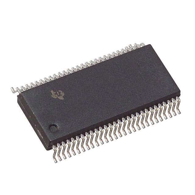
| 描述 | IC TRANSCVR TRI-ST 16BIT 56SSOP总线收发器 16bit Regisrered |
| 产品分类 | |
| 品牌 | Texas Instruments |
| 产品手册 | |
| 产品图片 |
|
| rohs | 符合RoHS无铅 / 符合限制有害物质指令(RoHS)规范要求 |
| 产品系列 | 逻辑集成电路,总线收发器,Texas Instruments CY74FCT162543CTPVC74FCT |
| 数据手册 | |
| 产品型号 | CY74FCT162543CTPVC |
| 产品种类 | 总线收发器 |
| 传播延迟时间 | 5.1 ns |
| 低电平输出电流 | 24 mA |
| 供应商器件封装 | 56-SSOP |
| 元件数 | 2 |
| 其它名称 | 296-33192-5 |
| 功能 | 16-Bit Latched Transceiver |
| 包装 | 管件 |
| 单位重量 | 694.800 mg |
| 商标 | Texas Instruments |
| 安装类型 | 表面贴装 |
| 安装风格 | SMD/SMT |
| 封装 | Tube |
| 封装/外壳 | 56-BSSOP(0.295",7.50mm 宽) |
| 封装/箱体 | SSOP-56 |
| 工作温度 | -40°C ~ 85°C |
| 工厂包装数量 | 20 |
| 最大功率耗散 | 1 W |
| 最大工作温度 | + 85 C |
| 最小工作温度 | - 40 C |
| 极性 | Non-Inverting |
| 标准包装 | 20 |
| 每元件位数 | 8 |
| 每芯片的通道数量 | 16 |
| 电压-电源 | 4.5 V ~ 5.5 V |
| 电流-输出高,低 | 24mA,24mA |
| 电源电压-最大 | 5.5 V |
| 电源电压-最小 | 4.5 V |
| 电路数量 | 2 |
| 系列 | CY74FCT162543T |
| 输入电平 | TTL |
| 输出电平 | TTL |
| 输出类型 | 3-State |
| 逻辑类型 | Registered Transceiver |
| 逻辑系列 | FCT |
| 高电平输出电流 | - 24 mA |


- 商务部:美国ITC正式对集成电路等产品启动337调查
- 曝三星4nm工艺存在良率问题 高通将骁龙8 Gen1或转产台积电
- 太阳诱电将投资9.5亿元在常州建新厂生产MLCC 预计2023年完工
- 英特尔发布欧洲新工厂建设计划 深化IDM 2.0 战略
- 台积电先进制程称霸业界 有大客户加持明年业绩稳了
- 达到5530亿美元!SIA预计今年全球半导体销售额将创下新高
- 英特尔拟将自动驾驶子公司Mobileye上市 估值或超500亿美元
- 三星加码芯片和SET,合并消费电子和移动部门,撤换高东真等 CEO
- 三星电子宣布重大人事变动 还合并消费电子和移动部门
- 海关总署:前11个月进口集成电路产品价值2.52万亿元 增长14.8%


PDF Datasheet 数据手册内容提取
Data sheet acquired from Cypress Semiconductor Corporation. CY74FCT16543T Data sheet modified to remove devices not offered. CY74FCT162543T CY74FCT162H543T 16-Bit Latched Transceivers SCCS059B - August 1994 - Revised September 2001 Features Functional Description • I supports partial-power-down mode operation The CY74FCT16543T and CY74FCT162543T are 16-bit, off • Edge-rate control circuitry for significantly improved high-speed,lowpowerlatchedtransceiversthatareorganizedastwo noise characteristics independent8-bitD-typelatchedtransceiverscontainingtwosetsof • Typical output skew < 250 ps eightD-typelatcheswithseparateLatchEnable(LEAB,LEAB)and Output Enable (OEAB, OEAB) controls for each set to permit • ESD > 2000V independentcontrolofinputtingandoutputtingineitherdirectionof • TSSOP (19.6-mil pitch) and SSOP (25-mil pitch) dataflow.FordataflowfromAtoB,forexample,theA-to-Binput packages Enable(CEAB)mustbeLOWinordertoenterdatafromAortotake • Industrial temperature range of−40˚C to +85˚C datafromBasindicatedinthetruthtable.WithCAEBLOW,aLOW • V = 5V± 10% signalontheA-to-BLatchEnable(LEAB)makestheA-to-Blatches CC transparent; a subsequent LOW-to-HIGH transition of the LEAB CY74FCT16543T Features: signalputstheAlatchesinthestoragemodeandtheiroutputsno • 64 mA sink current, 32 mA source current longerchangewiththeAinputs.WithCEABandOEABbothLOW, • Typical V (ground bounce) <1.0V at V = 5V, thethree-stateBoutputbuffersareactiveandreflectthedatapresent OLP CC T = 25˚C attheoutputoftheAlatches.ControlofdatafromBtoAissimilar, A butusesCEAB,LEAB,andOEABinputsflow-throughpinoutand CY74FCT162543T Features: small shrink packaging and in simplifying board design. • Balanced 24 mA output drivers This device is fully specified for partial-power-down • Reduced system switching noise applications using I . The I circuitry disables the outputs, off off • Typical V (ground bounce) <0.6V at V = 5V, preventing damaging current backflow through the device OLP CC T = 25˚C when it is powered down. A CY74FCT162H543T Features: The CY74FCT16543T is ideally suited for driving high-capacitance loads and low-impedance backplanes. • Bus hold retains last active state The CY74FCT162543T has 24-mA balanced output drivers • Eliminates the need for external pull-up or pull-down resistors withcurrentlimitingresistorsintheoutputs.Thisreducesthe need for external terminating resistors and provides for minimal undershoot and reduced ground bounce. The CY74FCT162543T is ideal for driving transmission lines. TheCY74FCT162H543Tisa24-mAbalancedoutputpartthat has “bus hold” on the data inputs. The device retains the input’slaststatewhenevertheinputgoestohighimpedance. This eliminates the need for pull-up/down resistors and prevents floating inputs. Copyright © 2001, Texas Instruments Incorporated
CY74FCT16543T CY74FCT162543T CY74FCT162H543T LogicBlockDiagrams PinConfiguration 1OEBA Top View 1CEBA SSOP/TSSOP 1LEBA 1OEAB 1OEAB 1 56 1OEBA 1CEAB 11CLEEAABB 23 5554 11LCEEBBAA 1LEAB GND 4 53 GND 1A1 C 1A1 5 52 1B1 D 1B1 1A2 6 51 1B2 VCC 7 50 VCC C 1A3 8 49 1B3 D 1A4 9 48 1B4 1A5 10 47 1B5 GND 11 46 GND 1A6 12 45 1B6 TO7OTHERCHANNELS 1A7 13 44 1B7 FCT16543T-1 1A8 14 43 1B8 2OEBA 2A1 15 42 2B1 2CEBA 2A2 16 41 2B2 2LEBA 2A3 17 40 2B3 GND 18 39 GND 2OEAB 2A4 19 38 2B4 2CEAB 2A5 20 37 2B5 2LEAB 2A6 21 36 2B6 C VCC 22 35 VCC 2A1 D 2B1 2A7 23 34 2B7 2A8 24 33 2B8 C GND 25 32 GND 2CEAB 26 31 2CEBA D 2LEAB 27 30 2LEBA 2OEAB 28 29 2OEBA TO 7OTHERCHANNELS FCT16543T-2 FCT16543T-3 Pin Description Function Table[1] Name Description Latch Output Inputs Status Buffers OEAB A-to-B Output Enable Input (Active LOW) CEAB LEAB OEAB A to B B OEBA B-to-A Output Enable Input (Active LOW) H X X Storing High Z CEAB A-to-B Enable Input (Active LOW) X H X Storing X CEBA B-to-A Enable Input (Active LOW) X X H X High Z LEAB A-to-B Latch Enable Input (Active LOW) L L L Transparent Current A LEBA B-to-A Latch Enable Input (Active LOW) Inputs A A-to-BDataInputsorB-to-AThree-StateOutputs[9] L H L Storing Previous A B B-to-ADataInputsorA-to-BThree-StateOutputs[9] Inputs[2] Maximum Ratings[3, 4] (Above which the useful life may be impaired. For user Power Dissipation..........................................................1.0W guidelines, not tested.) Static Discharge Voltage............................................>2001V Storage Temperature .....................Com’l −55°C to +125°C (per MIL-STD-883, Method 3015) Ambient Temperature with Operating Range Power Applied.................................Com’l −55°C to +125°C DC Input Voltage.................................................−0.5V to +7.0V Ambient Range Temperature V DC Output Voltage..............................................−0.5V to +7.0V CC Industrial −40°C to +85°C 5V± 10% DC Output Current (Maximum Sink Current/Pin)...........................−60 to +120 mA 2
CY74FCT16543T CY74FCT162543T CY74FCT162H543T Electrical Characteristics Over the Operating Range Parameter Description Test Conditions Min. Typ.[5] Max. Unit V Input HIGH Voltage 2.0 V IH V Input LOW Voltage 0.8 V IL V Input Hysteresis[6] 100 mV H V Input Clamp Diode Voltage V =Min., I =−18 mA −0.7 −1.2 V IK CC IN I Input HIGH Current V =Max., V=V ±1 µA IH CC I CC I Input LOW Current V =Max., V=GND ±1 µA IL CC I I High Impedance Output Cur- V =Max., V =2.7V ±1 µA OZH CC OUT rent (Three-State Output pins) I High Impedance Output Cur- V =Max., V =0.5V ±1 µA OZL CC OUT rent (Three-State Output pins) I Short Circuit Current[7] V =Max., V =GND −80 −140 −200 mA OS CC OUT I Output Drive Current[7] V =Max., V =2.5V −50 −180 mA O CC OUT I Power-Off Disable V =0V, V ≤4.5V[8] ±1 µA OFF CC OUT Notes: 1. A-to-B data flow shown; B-to-A flow control is the same, except usingCEBA, LEBA, and OEBA. 2. Data prior toLEAB LOW-to-HIGH Transition H = HIGH Voltage Level. L = LOW Voltage Level. X = Don’t Care. Z = High Impedance. 3. Operationbeyondthelimitssetforthmayimpairtheusefullifeofthedevice.Unlessotherwisenoted,theselimitsareovertheoperatingfree-airtemperature range. 4. Unused inputs must always be connected to an appropriate logic voltage level, preferably either VCC or ground. 5. Typical values are at VCC= 5.0V, TA= +25˚C ambient. 6. This parameter is specified but not tested. 7. Notmorethanoneoutputshouldbeshortedatatime.Durationofshortshouldnotexceedonesecond.Theuseofhigh-speedtestapparatusand/orsample and hold techniques are preferable in order to minimize internal chip heating and more accurately reflect operational values. Otherwise prolonged shorting ofahighoutputmayraisethechiptemperaturewellabovenormalandtherebycauseinvalidreadingsinotherparametrictests.Inanysequenceofparameter tests, IOS tests should be performed last. 8. Tested at +25˚C. 9. On the 74FCT162H543T, these pins have bus hold. 3
CY74FCT16543T CY74FCT162543T CY74FCT162H543T Output Drive Characteristics for CY74FCT16543T Parameter Description Test Conditions Min. Typ.[5] Max. Unit V Output HIGH Voltage V =Min., I =−3 mA 2.5 3.5 V OH CC OH V =Min., I =−15 mA 2.4 3.5 CC OH V =Min., I =−32 mA 2.0 3.0 CC OH V Output LOW Voltage V =Min., I =64 mA 0.2 0.55 V OL CC OL Output Drive Characteristics for CY74FCT162543T, CY74FCT162H543T Parameter Description Test Conditions Min. Typ.[5] Max. Unit I Output LOW Current[7] V =5V, V =V or V , V =1.5V 60 115 150 mA ODL CC IN IH IL OUT I Output HIGH Current[7] V =5V, V =V or V , V =1.5V −60 −115 −150 mA ODH CC IN IH IL OUT V Output HIGH Voltage V =Min., I =−24 mA 2.4 3.3 V OH CC OH V Output LOW Voltage V =Min., I =24 mA 0.3 0.55 V OL CC OL Capacitance[6](T = +25˚C, f = 1.0 MHz) A Parameter Description Test Conditions Typ.[5] Max. Unit C Input Capacitance V = 0V 4.5 6.0 pF IN IN C Output Capacitance V = 0V 5.5 8.0 pF OUT OUT Power Supply Characteristics Parameter Description Test Conditions Typ.[5] Max. Unit I QuiescentPowerSupplyCurrent V =Max. V ≤0.2V, 5 500 µA CC CC IN V ≥V −0.2V IN CC ∆I QuiescentPowerSupplyCurrent V =Max. V =3.4V[10] 0.5 1.5 mA CC CC IN (TTL inputs HIGH) I Dynamic Power Supply V =Max., One Input V =V or 60 100 µA/MHz CCD CC IN CC Current[11] Toggling, 50% Duty Cycle, V =GND IN Outputs Open,OE=GND I Total Power Supply Current[12] V =Max., f =10 MHz, V =V or 0.6 1.5 mA C CC 1 IN CC 50% Duty Cycle, Outputs V =GND IN Open, One Bit Toggling, V =3.4V or 0.9 2.3 mA OE=GND IN V =GND IN V =Max., f =2.5 MHz, V =V or 2.4 4.5[13] mA CC 1 IN CC 50% Duty Cycle, Outputs V =GND IN Open, Sixteen Bits Toggling, V =3.4V or 6.4 16.5[13] mA OE=GND IN V =GND IN Notes: 10. Per TTL driven input (VIN=3.4V); all other inputs at VCC or GND. 11. This parameter is not directly testable, but is derived for use in Total Power Supply calculations. 12. IICC == IIQCUCI+E∆SICCECNDTH +N ITIN+PICUCTDS(+f0 /I2D Y+N fA1MNI1C) ICC = Quiescent Current with CMOS input levels ∆ICC = Power Supply Current for a TTL HIGH input (VIN=3.4V) DH = Duty Cycle for TTL inputs HIGH NT = Number of TTL inputs at DH ICCD = Dynamic Current caused by an input transition pair (HLH or LHL) f0 = Clock frequency for registered devices, otherwise zero f1 = Input signal frequency N1 = Number of inputs changing at f1 All currents are in milliamps and all frequencies are in megahertz. 13. Values for these conditions are examples of the ICC formula. These limits are specified but not tested. 4
CY74FCT16543T CY74FCT162543T CY74FCT162H543T Switching Characteristics Over the Operating Range[14] CY74FCT16543T CY74FCT16543AT CY74FCT162543T CY74FCT162543AT Fig. Parameter Description Min. Max. Min. Max. Unit No.[15] t Propagation Delay 1.5 8.5 1.5 6.5 ns 1, 3 PLH t Transparent Mode PHL A to B or B to A t Propagation Delay 1.5 12.5 1.5 8.0 ns 1, 5 PLH t LEBA to A,LEAB to B PHL t Output Enable Time 1.5 12.0 1.5 9.0 ns 1, 7, 8 PZH t OEBA orOEAB to A or B PZL CEBA orCEAB to A or B t Output Disable Time 1.5 9.0 1.5 7.5 ns 1, 7, 8 PHZ t OEBA orOEAB to A or B PLZ CEBA orCEAB to A or B t Set-up Time HIGH or LOW 2.0 — 2.0 — ns 4 SU A or B toLEAB orLEBA t Hold Time HIGH or LOW 2.0 — 2.0 — ns 4 H A or B toLEAB orLEBA t LEBA orLEAB Pulse Width LOW 4.0 — 4.0 — ns 5 W t Output Skew[16] — 0.5 — 0.5 ns — SK(O) CY74FCT16543CT CY74FCT162543CT CY74FCT162H543CT Fig. Parameter Description Min. Max. Unit No.[15] t Propagation Delay 1.5 5.1 ns 1, 3 PLH t Transparent Mode PHL A to B or B to A t Propagation Delay 1.5 5.6 ns 1, 5 PLH t LEBA to A,LEAB to B PHL t Output Enable Time 1.5 7.8 ns 1, 7, 8 PZH t OEBA orOEAB to A or B PZL CEBA orCEAB to A or B t Output Disable Time 1.5 6.5 ns 1, 7, 8 PHZ t OEBA orOEAB to A or B PLZ CEBA orCEAB to A or B t Set-up Time HIGH or LOW 2.0 — ns 4 SU A or B toLEAB orLEBA t Hold Time HIGH or LOW 2.0 — ns 4 H A or B toLEAB orLEBA t LEBA orLEAB Pulse Width LOW 4.0 — ns 5 W t Output Skew[16] — 0.5 ns — SK(O) Notes: 14. Minimum limits are specified but not tested on Propagation Delays. 15. See “Parameter Measurement Information” in the General Information section. 16. Skew between any two outputs of the same package switching in the same directional. This parameter is ensured by design. 5
CY74FCT16543T CY74FCT162543T CY74FCT162H543T Ordering Information CY74FCT16543 Speed Package Operating (ns) Ordering Code Name Package Type Range 5.1 CY74FCT16543CTPVC/PVCT O56 56-Lead (300-Mil) SSOP Industrial 6.5 CY74FCT16543ATPACT Z56 56-Lead (240-Mil) TSSOP Industrial 8.5 CY74FCT16543TPVC/PVCT O56 56-Lead (300-Mil) SSOP Industrial Ordering Information CY74FCT162543 Speed Package Operating (ns) Ordering Code Name Package Type Range 5.1 74FCT162543CTPACT Z56 56-Lead (240-Mil) TSSOP Industrial CY74FCT162543CTPVC O56 56-Lead (300-Mil) SSOP 74FCT162543CTPVCT O56 56-Lead (300-Mil) SSOP 6.5 74FCT162543ATPACT Z56 56-Lead (240-Mil) TSSOP Industrial 8.5 CY74FCT162543TPVC/PVCT O56 56-Lead (300-Mil) SSOP Industrial Ordering Information CY74FCT162H543T Speed Package Operating (ns) Ordering Code Name Package Type Range 5.1 74FCT162H543CTPACT Z56 56-Lead (240-Mil) TSSOP Industrial 6
CY74FCT16543T CY74FCT162543T CY74FCT162H543T Package Diagrams 56-LeadShrunkSmallOutlinePackageO56 56-LeadThinShrunkSmallOutline PackageZ56 7
PACKAGE OPTION ADDENDUM www.ti.com 27-Sep-2007 PACKAGING INFORMATION OrderableDevice Status(1) Package Package Pins Package EcoPlan(2) Lead/BallFinish MSLPeakTemp(3) Type Drawing Qty 74FCT162543ATPACT ACTIVE TSSOP DGG 56 2000 Green(RoHS& CUNIPDAU Level-1-260C-UNLIM noSb/Br) 74FCT162543CTPACT ACTIVE TSSOP DGG 56 2000 Green(RoHS& CUNIPDAU Level-1-260C-UNLIM noSb/Br) 74FCT162543CTPVCG4 ACTIVE SSOP DL 56 20 Green(RoHS& CUNIPDAU Level-1-260C-UNLIM noSb/Br) 74FCT162543CTPVCT ACTIVE SSOP DL 56 1000 Green(RoHS& CUNIPDAU Level-1-260C-UNLIM noSb/Br) 74FCT162543ETPACT OBSOLETE TSSOP DGG 56 TBD CallTI CallTI 74FCT162543ETPVCT OBSOLETE SSOP DL 56 TBD CallTI CallTI 74FCT162543TPVCG4 ACTIVE SSOP DL 56 20 Green(RoHS& CUNIPDAU Level-1-260C-UNLIM noSb/Br) 74FCT162543TPVCTG4 ACTIVE SSOP DL 56 1000 Green(RoHS& CUNIPDAU Level-1-260C-UNLIM noSb/Br) 74FCT162H543CTPACT ACTIVE TSSOP DGG 56 2000 Green(RoHS& CUNIPDAU Level-1-260C-UNLIM noSb/Br) 74FCT16543ATPACTE4 ACTIVE TSSOP DGG 56 2000 Green(RoHS& CUNIPDAU Level-1-260C-UNLIM noSb/Br) 74FCT16543ATPACTG4 ACTIVE TSSOP DGG 56 2000 Green(RoHS& CUNIPDAU Level-1-260C-UNLIM noSb/Br) 74FCT16543CTPVCG4 ACTIVE SSOP DL 56 20 Green(RoHS& CUNIPDAU Level-1-260C-UNLIM noSb/Br) 74FCT16543CTPVCTG4 ACTIVE SSOP DL 56 1000 Green(RoHS& CUNIPDAU Level-1-260C-UNLIM noSb/Br) 74FCT16543TPVCG4 ACTIVE SSOP DL 56 20 Green(RoHS& CUNIPDAU Level-1-260C-UNLIM noSb/Br) 74FCT16543TPVCTG4 ACTIVE SSOP DL 56 1000 Green(RoHS& CUNIPDAU Level-1-260C-UNLIM noSb/Br) CY74FCT162543CTPVC ACTIVE SSOP DL 56 20 Green(RoHS& CUNIPDAU Level-1-260C-UNLIM noSb/Br) CY74FCT162543ETPAC OBSOLETE TSSOP DGG 56 TBD CallTI CallTI CY74FCT162543ETPVC OBSOLETE SSOP DL 56 TBD CallTI CallTI CY74FCT162543TPVC ACTIVE SSOP DL 56 20 Green(RoHS& CUNIPDAU Level-1-260C-UNLIM noSb/Br) CY74FCT162543TPVCT ACTIVE SSOP DL 56 1000 Green(RoHS& CUNIPDAU Level-1-260C-UNLIM noSb/Br) CY74FCT16543ATPACT ACTIVE TSSOP DGG 56 2000 Green(RoHS& CUNIPDAU Level-1-260C-UNLIM noSb/Br) CY74FCT16543CTPVC ACTIVE SSOP DL 56 20 Green(RoHS& CUNIPDAU Level-1-260C-UNLIM noSb/Br) CY74FCT16543CTPVCT ACTIVE SSOP DL 56 1000 Green(RoHS& CUNIPDAU Level-1-260C-UNLIM noSb/Br) CY74FCT16543ETPAC OBSOLETE TSSOP DGG 56 TBD CallTI CallTI CY74FCT16543ETPACT OBSOLETE TSSOP DGG 56 TBD CallTI CallTI CY74FCT16543ETPVC OBSOLETE SSOP DL 56 TBD CallTI CallTI CY74FCT16543ETPVCT OBSOLETE SSOP DL 56 TBD CallTI CallTI CY74FCT16543TPVC ACTIVE SSOP DL 56 20 Green(RoHS& CUNIPDAU Level-1-260C-UNLIM noSb/Br) Addendum-Page1
PACKAGE OPTION ADDENDUM www.ti.com 27-Sep-2007 OrderableDevice Status(1) Package Package Pins Package EcoPlan(2) Lead/BallFinish MSLPeakTemp(3) Type Drawing Qty CY74FCT16543TPVCT ACTIVE SSOP DL 56 1000 Green(RoHS& CUNIPDAU Level-1-260C-UNLIM noSb/Br) FCT162543ATPACTE4 ACTIVE TSSOP DGG 56 2000 Green(RoHS& CUNIPDAU Level-1-260C-UNLIM noSb/Br) FCT162543ATPACTG4 ACTIVE TSSOP DGG 56 2000 Green(RoHS& CUNIPDAU Level-1-260C-UNLIM noSb/Br) FCT162543CTPACTE4 ACTIVE TSSOP DGG 56 2000 Green(RoHS& CUNIPDAU Level-1-260C-UNLIM noSb/Br) FCT162543CTPACTG4 ACTIVE TSSOP DGG 56 2000 Green(RoHS& CUNIPDAU Level-1-260C-UNLIM noSb/Br) FCT162543CTPVCTG4 ACTIVE SSOP DL 56 1000 Green(RoHS& CUNIPDAU Level-1-260C-UNLIM noSb/Br) FCT162H543CTPACTE4 ACTIVE TSSOP DGG 56 2000 Green(RoHS& CUNIPDAU Level-1-260C-UNLIM noSb/Br) FCT162H543CTPACTG4 ACTIVE TSSOP DGG 56 2000 Green(RoHS& CUNIPDAU Level-1-260C-UNLIM noSb/Br) (1)Themarketingstatusvaluesaredefinedasfollows: ACTIVE:Productdevicerecommendedfornewdesigns. LIFEBUY:TIhasannouncedthatthedevicewillbediscontinued,andalifetime-buyperiodisineffect. NRND:Notrecommendedfornewdesigns.Deviceisinproductiontosupportexistingcustomers,butTIdoesnotrecommendusingthispartin anewdesign. PREVIEW:Devicehasbeenannouncedbutisnotinproduction.Samplesmayormaynotbeavailable. OBSOLETE:TIhasdiscontinuedtheproductionofthedevice. (2)EcoPlan-Theplannedeco-friendlyclassification:Pb-Free(RoHS),Pb-Free(RoHSExempt),orGreen(RoHS&noSb/Br)-pleasecheck http://www.ti.com/productcontentforthelatestavailabilityinformationandadditionalproductcontentdetails. TBD:ThePb-Free/Greenconversionplanhasnotbeendefined. Pb-Free(RoHS):TI'sterms"Lead-Free"or"Pb-Free"meansemiconductorproductsthatarecompatiblewiththecurrentRoHSrequirements forall6substances,includingtherequirementthatleadnotexceed0.1%byweightinhomogeneousmaterials.Wheredesignedtobesoldered athightemperatures,TIPb-Freeproductsaresuitableforuseinspecifiedlead-freeprocesses. Pb-Free(RoHSExempt):ThiscomponenthasaRoHSexemptionforeither1)lead-basedflip-chipsolderbumpsusedbetweenthedieand package, or 2) lead-based die adhesive used between the die and leadframe. The component is otherwise considered Pb-Free (RoHS compatible)asdefinedabove. Green(RoHS&noSb/Br):TIdefines"Green"tomeanPb-Free(RoHScompatible),andfreeofBromine(Br)andAntimony(Sb)basedflame retardants(BrorSbdonotexceed0.1%byweightinhomogeneousmaterial) (3) MSL, Peak Temp. -- The Moisture Sensitivity Level rating according to the JEDEC industry standard classifications, and peak solder temperature. Important Information and Disclaimer:The information provided on this page represents TI's knowledge and belief as of the date that it is provided. TI bases its knowledge and belief on information provided by third parties, and makes no representation or warranty as to the accuracy of such information. Efforts are underway to better integrate information from third parties. TI has taken and continues to take reasonable steps to provide representative and accurate information but may not have conducted destructive testing or chemical analysis on incomingmaterialsandchemicals.TIandTIsuppliersconsidercertaininformationtobeproprietary,andthusCASnumbersandotherlimited informationmaynotbeavailableforrelease. InnoeventshallTI'sliabilityarisingoutofsuchinformationexceedthetotalpurchasepriceoftheTIpart(s)atissueinthisdocumentsoldbyTI toCustomeronanannualbasis. Addendum-Page2
PACKAGE MATERIALS INFORMATION www.ti.com 11-Mar-2008 TAPE AND REEL INFORMATION *Alldimensionsarenominal Device Package Package Pins SPQ Reel Reel A0(mm) B0(mm) K0(mm) P1 W Pin1 Type Drawing Diameter Width (mm) (mm) Quadrant (mm) W1(mm) 74FCT162543ATPACT TSSOP DGG 56 2000 330.0 24.4 8.6 15.6 1.8 12.0 24.0 Q1 74FCT162543CTPACT TSSOP DGG 56 2000 330.0 24.4 8.6 15.6 1.8 12.0 24.0 Q1 74FCT162543CTPVCT SSOP DL 56 1000 330.0 32.4 11.35 18.67 3.1 16.0 32.0 Q1 74FCT162H543CTPACT TSSOP DGG 56 2000 330.0 24.4 8.6 15.6 1.8 12.0 24.0 Q1 CY74FCT162543TPVCT SSOP DL 56 1000 330.0 32.4 11.35 18.67 3.1 16.0 32.0 Q1 CY74FCT16543ATPACT TSSOP DGG 56 2000 330.0 24.4 8.6 15.6 1.8 12.0 24.0 Q1 CY74FCT16543CTPVCT SSOP DL 56 1000 330.0 32.4 11.35 18.67 3.1 16.0 32.0 Q1 CY74FCT16543TPVCT SSOP DL 56 1000 330.0 32.4 11.35 18.67 3.1 16.0 32.0 Q1 PackMaterials-Page1
PACKAGE MATERIALS INFORMATION www.ti.com 11-Mar-2008 *Alldimensionsarenominal Device PackageType PackageDrawing Pins SPQ Length(mm) Width(mm) Height(mm) 74FCT162543ATPACT TSSOP DGG 56 2000 346.0 346.0 41.0 74FCT162543CTPACT TSSOP DGG 56 2000 346.0 346.0 41.0 74FCT162543CTPVCT SSOP DL 56 1000 346.0 346.0 49.0 74FCT162H543CTPACT TSSOP DGG 56 2000 346.0 346.0 41.0 CY74FCT162543TPVCT SSOP DL 56 1000 346.0 346.0 49.0 CY74FCT16543ATPACT TSSOP DGG 56 2000 346.0 346.0 41.0 CY74FCT16543CTPVCT SSOP DL 56 1000 346.0 346.0 49.0 CY74FCT16543TPVCT SSOP DL 56 1000 346.0 346.0 49.0 PackMaterials-Page2
MECHANICAL DATA MTSS003D – JANUARY 1995 – REVISED JANUARY 1998 DGG (R-PDSO-G**) PLASTIC SMALL-OUTLINE PACKAGE 48 PINS SHOWN 0,27 0,50 0,08 M 0,17 48 25 6,20 8,30 6,00 7,90 0,15 NOM Gage Plane 0,25 1 24 0°–8° A 0,75 0,50 Seating Plane 0,15 1,20 MAX 0,10 0,05 PINS ** 48 56 64 DIM A MAX 12,60 14,10 17,10 A MIN 12,40 13,90 16,90 4040078/F 12/97 NOTES: A. All linear dimensions are in millimeters. B. This drawing is subject to change without notice. C. Body dimensions do not include mold protrusion not to exceed 0,15. D. Falls within JEDEC MO-153 • POST OFFICE BOX 655303 DALLAS, TEXAS 75265
MECHANICAL DATA MSSO001C – JANUARY 1995 – REVISED DECEMBER 2001 DL (R-PDSO-G**) PLASTIC SMALL-OUTLINE PACKAGE 48 PINS SHOWN 0.025 (0,635) 0.0135 (0,343) 0.005 (0,13) M 0.008 (0,203) 48 25 0.010 (0,25) 0.005 (0,13) 0.299 (7,59) 0.291 (7,39) 0.420 (10,67) 0.395 (10,03) Gage Plane 0.010 (0,25) 1 24 0°–(cid:1)8° 0.040 (1,02) A 0.020 (0,51) Seating Plane 0.004 (0,10) 0.110 (2,79) MAX 0.008 (0,20) MIN PINS ** 28 48 56 DIM 0.380 0.630 0.730 A MAX (9,65) (16,00) (18,54) 0.370 0.620 0.720 A MIN (9,40) (15,75) (18,29) 4040048/E 12/01 NOTES: A. All linear dimensions are in inches (millimeters). B. This drawing is subject to change without notice. C. Body dimensions do not include mold flash or protrusion not to exceed 0.006 (0,15). D. Falls within JEDEC MO-118 • POST OFFICE BOX 655303 DALLAS, TEXAS 75265
PACKAGE OPTION ADDENDUM www.ti.com 6-Feb-2020 PACKAGING INFORMATION Orderable Device Status Package Type Package Pins Package Eco Plan Lead/Ball Finish MSL Peak Temp Op Temp (°C) Device Marking Samples (1) Drawing Qty (2) (6) (3) (4/5) 74FCT162543ATPACT ACTIVE TSSOP DGG 56 2000 Green (RoHS NIPDAU Level-1-260C-UNLIM -40 to 85 FCT162543A & no Sb/Br) 74FCT162543CTPACT ACTIVE TSSOP DGG 56 2000 Green (RoHS NIPDAU Level-1-260C-UNLIM -40 to 85 FCT162543C & no Sb/Br) 74FCT16543ATPACTG4 ACTIVE TSSOP DGG 56 2000 Green (RoHS NIPDAU Level-1-260C-UNLIM -40 to 85 FCT16543A & no Sb/Br) CY74FCT162543CTPVC ACTIVE SSOP DL 56 20 Green (RoHS NIPDAU Level-1-260C-UNLIM -40 to 85 FCT162543C & no Sb/Br) CY74FCT162543TPVC ACTIVE SSOP DL 56 20 Green (RoHS NIPDAU Level-1-260C-UNLIM -40 to 85 FCT162543 & no Sb/Br) CY74FCT162543TPVCT ACTIVE SSOP DL 56 1000 Green (RoHS NIPDAU Level-1-260C-UNLIM -40 to 85 FCT162543 & no Sb/Br) CY74FCT16543ATPACT ACTIVE TSSOP DGG 56 2000 Green (RoHS NIPDAU Level-1-260C-UNLIM -40 to 85 FCT16543A & no Sb/Br) CY74FCT16543CTPVC ACTIVE SSOP DL 56 20 Green (RoHS NIPDAU Level-1-260C-UNLIM -40 to 85 FCT16543C & no Sb/Br) CY74FCT16543CTPVCT ACTIVE SSOP DL 56 1000 Green (RoHS NIPDAU Level-1-260C-UNLIM -40 to 85 FCT16543C & no Sb/Br) CY74FCT16543TPVC ACTIVE SSOP DL 56 20 Green (RoHS NIPDAU Level-1-260C-UNLIM -40 to 85 FCT16543 & no Sb/Br) (1) The marketing status values are defined as follows: ACTIVE: Product device recommended for new designs. LIFEBUY: TI has announced that the device will be discontinued, and a lifetime-buy period is in effect. NRND: Not recommended for new designs. Device is in production to support existing customers, but TI does not recommend using this part in a new design. PREVIEW: Device has been announced but is not in production. Samples may or may not be available. OBSOLETE: TI has discontinued the production of the device. (2) RoHS: TI defines "RoHS" to mean semiconductor products that are compliant with the current EU RoHS requirements for all 10 RoHS substances, including the requirement that RoHS substance do not exceed 0.1% by weight in homogeneous materials. Where designed to be soldered at high temperatures, "RoHS" products are suitable for use in specified lead-free processes. TI may reference these types of products as "Pb-Free". RoHS Exempt: TI defines "RoHS Exempt" to mean products that contain lead but are compliant with EU RoHS pursuant to a specific EU RoHS exemption. Green: TI defines "Green" to mean the content of Chlorine (Cl) and Bromine (Br) based flame retardants meet JS709B low halogen requirements of <=1000ppm threshold. Antimony trioxide based flame retardants must also meet the <=1000ppm threshold requirement. (3) MSL, Peak Temp. - The Moisture Sensitivity Level rating according to the JEDEC industry standard classifications, and peak solder temperature. Addendum-Page 1
PACKAGE OPTION ADDENDUM www.ti.com 6-Feb-2020 (4) There may be additional marking, which relates to the logo, the lot trace code information, or the environmental category on the device. (5) Multiple Device Markings will be inside parentheses. Only one Device Marking contained in parentheses and separated by a "~" will appear on a device. If a line is indented then it is a continuation of the previous line and the two combined represent the entire Device Marking for that device. (6) Lead/Ball Finish - Orderable Devices may have multiple material finish options. Finish options are separated by a vertical ruled line. Lead/Ball Finish values may wrap to two lines if the finish value exceeds the maximum column width. Important Information and Disclaimer:The information provided on this page represents TI's knowledge and belief as of the date that it is provided. TI bases its knowledge and belief on information provided by third parties, and makes no representation or warranty as to the accuracy of such information. Efforts are underway to better integrate information from third parties. TI has taken and continues to take reasonable steps to provide representative and accurate information but may not have conducted destructive testing or chemical analysis on incoming materials and chemicals. TI and TI suppliers consider certain information to be proprietary, and thus CAS numbers and other limited information may not be available for release. In no event shall TI's liability arising out of such information exceed the total purchase price of the TI part(s) at issue in this document sold by TI to Customer on an annual basis. Addendum-Page 2
PACKAGE MATERIALS INFORMATION www.ti.com 10-Aug-2016 TAPE AND REEL INFORMATION *Alldimensionsarenominal Device Package Package Pins SPQ Reel Reel A0 B0 K0 P1 W Pin1 Type Drawing Diameter Width (mm) (mm) (mm) (mm) (mm) Quadrant (mm) W1(mm) 74FCT162543ATPACT TSSOP DGG 56 2000 330.0 24.4 8.6 15.6 1.8 12.0 24.0 Q1 74FCT162543CTPACT TSSOP DGG 56 2000 330.0 24.4 8.6 15.6 1.8 12.0 24.0 Q1 CY74FCT162543TPVCT SSOP DL 56 1000 330.0 32.4 11.35 18.67 3.1 16.0 32.0 Q1 CY74FCT16543ATPACT TSSOP DGG 56 2000 330.0 24.4 8.6 15.6 1.8 12.0 24.0 Q1 CY74FCT16543CTPVCT SSOP DL 56 1000 330.0 32.4 11.35 18.67 3.1 16.0 32.0 Q1 PackMaterials-Page1
PACKAGE MATERIALS INFORMATION www.ti.com 10-Aug-2016 *Alldimensionsarenominal Device PackageType PackageDrawing Pins SPQ Length(mm) Width(mm) Height(mm) 74FCT162543ATPACT TSSOP DGG 56 2000 367.0 367.0 45.0 74FCT162543CTPACT TSSOP DGG 56 2000 367.0 367.0 45.0 CY74FCT162543TPVCT SSOP DL 56 1000 367.0 367.0 55.0 CY74FCT16543ATPACT TSSOP DGG 56 2000 367.0 367.0 45.0 CY74FCT16543CTPVCT SSOP DL 56 1000 367.0 367.0 55.0 PackMaterials-Page2
None
PACKAGE OUTLINE DGG0056A TSSOP - 1.2 mm max height SCALE 1.200 SMALL OUTLINE PACKAGE C 8.3 SEATING PLANE TYP 7.9 A PIN 1 ID 0.1 C AREA 54X 0.5 56 1 14.1 2X 13.9 13.5 NOTE 3 28 29 0.27 B 6.2 56X 0.17 1.2 MAX 6.0 0.08 C A B (0.15) TYP 0.25 SEE DETAIL A GAGE PLANE 0.15 0.75 0 - 8 0.05 0.50 DETAIL A TYPICAL 4222167/A 07/2015 NOTES: 1. All linear dimensions are in millimeters. Any dimensions in parenthesis are for reference only. Dimensioning and tolerancing per ASME Y14.5M. 2. This drawing is subject to change without notice. 3. This dimension does not include mold flash, protrusions, or gate burrs. Mold flash, protrusions, or gate burrs shall not exceed 0.15 mm per side. 4. Reference JEDEC registration MO-153. www.ti.com
EXAMPLE BOARD LAYOUT DGG0056A TSSOP - 1.2 mm max height SMALL OUTLINE PACKAGE 56X (1.5) SYMM 1 56 56X (0.3) 54X (0.5) (R0.05) TYP SYMM 28 29 (7.5) LAND PATTERN EXAMPLE SCALE:6X SOOPLEDNEINRG MASK METAL MSOELTDAEL RU NMDAESRK SOOPLEDNEINRG MASK 0.05 MAX 0.05 MIN ALL AROUND ALL AROUND NON SOLDER MASK SOLDER MASK DEFINED DEFINED SOLDER MASK DETAILS 4222167/A 07/2015 NOTES: (continued) 5. Publication IPC-7351 may have alternate designs. 6. Solder mask tolerances between and around signal pads can vary based on board fabrication site. www.ti.com
EXAMPLE STENCIL DESIGN DGG0056A TSSOP - 1.2 mm max height SMALL OUTLINE PACKAGE 56X (1.5) SYMM 1 56 56X (0.3) 54X (0.5) (R0.05) TYP SYMM 28 29 (7.5) SOLDER PASTE EXAMPLE BASED ON 0.125 mm THICK STENCIL SCALE:6X 4222167/A 07/2015 NOTES: (continued) 7. Laser cutting apertures with trapezoidal walls and rounded corners may offer better paste release. IPC-7525 may have alternate design recommendations. 8. Board assembly site may have different recommendations for stencil design. www.ti.com
IMPORTANTNOTICEANDDISCLAIMER TI PROVIDES TECHNICAL AND RELIABILITY DATA (INCLUDING DATASHEETS), DESIGN RESOURCES (INCLUDING REFERENCE DESIGNS), APPLICATION OR OTHER DESIGN ADVICE, WEB TOOLS, SAFETY INFORMATION, AND OTHER RESOURCES “AS IS” AND WITH ALL FAULTS, AND DISCLAIMS ALL WARRANTIES, EXPRESS AND IMPLIED, INCLUDING WITHOUT LIMITATION ANY IMPLIED WARRANTIES OF MERCHANTABILITY, FITNESS FOR A PARTICULAR PURPOSE OR NON-INFRINGEMENT OF THIRD PARTY INTELLECTUAL PROPERTY RIGHTS. These resources are intended for skilled developers designing with TI products. You are solely responsible for (1) selecting the appropriate TI products for your application, (2) designing, validating and testing your application, and (3) ensuring your application meets applicable standards, and any other safety, security, or other requirements. These resources are subject to change without notice. TI grants you permission to use these resources only for development of an application that uses the TI products described in the resource. Other reproduction and display of these resources is prohibited. No license is granted to any other TI intellectual property right or to any third party intellectual property right. TI disclaims responsibility for, and you will fully indemnify TI and its representatives against, any claims, damages, costs, losses, and liabilities arising out of your use of these resources. TI’s products are provided subject to TI’s Terms of Sale (www.ti.com/legal/termsofsale.html) or other applicable terms available either on ti.com or provided in conjunction with such TI products. TI’s provision of these resources does not expand or otherwise alter TI’s applicable warranties or warranty disclaimers for TI products. Mailing Address: Texas Instruments, Post Office Box 655303, Dallas, Texas 75265 Copyright © 2020, Texas Instruments Incorporated