ICGOO在线商城 > 集成电路(IC) > PMIC - 稳压器 - 线性 > MAX1726EUK33+T

 Datasheet下载
- 型号: MAX1726EUK33+T
- 制造商: Maxim
- 库位|库存: xxxx|xxxx
- 要求:
| 数量阶梯 | 香港交货 | 国内含税 |
| +xxxx | $xxxx | ¥xxxx |
查看当月历史价格
查看今年历史价格
MAX1726EUK33+T产品简介:
ICGOO电子元器件商城为您提供MAX1726EUK33+T由Maxim设计生产,在icgoo商城现货销售,并且可以通过原厂、代理商等渠道进行代购。 MAX1726EUK33+T价格参考。MaximMAX1726EUK33+T封装/规格:PMIC - 稳压器 - 线性, Linear Voltage Regulator IC Positive Fixed 1 Output 3.3V 20mA SOT-23-5。您可以下载MAX1726EUK33+T参考资料、Datasheet数据手册功能说明书,资料中有MAX1726EUK33+T 详细功能的应用电路图电压和使用方法及教程。
Maxim Integrated的MAX1726EUK33+T是一款线性稳压器(LDO),属于电源管理集成电路(PMIC)的一部分。该器件输出电压为3.3V,具有低噪声、低压差和高电源抑制比(PSRR)等特点,适用于对电源稳定性和噪声敏感的应用场景。

主要应用场景包括:

1. 便携式电子设备:如智能手机、平板电脑、手持仪表等,用于为微处理器、传感器或射频模块提供稳定电源。
2. 通信设备:在无线基站、路由器或光模块中,为低功耗射频芯片或模拟前端提供干净电源。
3. 工业控制系统:如PLC、工业传感器和测量仪器,适用于需要高稳定性和抗干扰能力的工业环境。
4. 汽车电子系统:如车载信息娱乐系统、驾驶辅助模块等,满足汽车环境中对电源可靠性的要求。
5. 医疗设备:用于便携式或可穿戴医疗设备,如血糖仪、心率监测仪等,确保低噪声供电以提高测量精度。

该器件采用小型TSOT封装,适合空间受限的设计,同时具备良好的热稳定性和负载瞬态响应能力,是一款高性价比的电源解决方案。
| 参数 | 数值 |
| 产品目录 | 集成电路 (IC)半导体 |
| 描述 | IC REG LDO 3.3V 20MA SOT23-5低压差稳压器 12V Ultra-Low-IQ |
| 产品分类 | |
| 品牌 | Maxim Integrated |
| 产品手册 | |
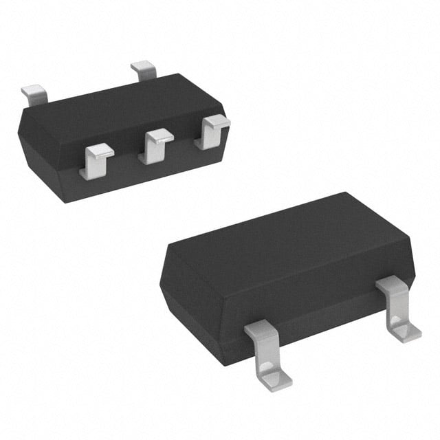
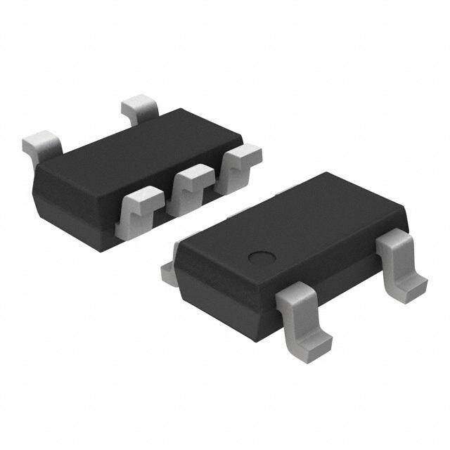
| 产品图片 |
|
| rohs | 符合RoHS无铅 / 符合限制有害物质指令(RoHS)规范要求 |
| 产品系列 | 电源管理 IC,低压差稳压器,Maxim Integrated MAX1726EUK33+T- |
| 数据手册 | |
| 产品型号 | MAX1726EUK33+T |
| 产品培训模块 | http://www.digikey.cn/PTM/IndividualPTM.page?site=cn&lang=zhs&ptm=25703http://www.digikey.cn/PTM/IndividualPTM.page?site=cn&lang=zhs&ptm=25705 |
| 产品种类 | 低压差稳压器 |
| 供应商器件封装 | SOT-23-5 |
| 其它名称 | MAX1726EUK33+TDKR |
| 包装 | Digi-Reel® |
| 商标 | Maxim Integrated |
| 回动电压—最大值 | 600 mV at 20 mA |
| 安装类型 | 表面贴装 |
| 安装风格 | SMD/SMT |
| 封装 | Reel |
| 封装/外壳 | SC-74A,SOT-753 |
| 封装/箱体 | SOT-23-5 |
| 工作温度 | -40°C ~ 85°C |
| 工厂包装数量 | 2500 |
| 应用说明 | |
| 最大功率耗散 | 0.571 W |
| 最大工作温度 | + 85 C |
| 最大输入电压 | 12 V |
| 最小工作温度 | - 40 C |
| 最小输入电压 | + 2.5 V |
| 标准包装 | 1 |
| 电压-跌落(典型值) | 0.3V @ 20mA |
| 电压-输入 | 最高 12V |
| 电压-输出 | 3.3V |
| 电压调节准确度 | 1.5 % |
| 电流-输出 | 20mA |
| 电流-限制(最小值) | - |
| 稳压器拓扑 | 正,固定式 |
| 稳压器数 | 1 |
| 系列 | MAX1726 |
| 线路调整率 | 0.01 % / V |
| 负载调节 | 0.015 % / mA |
| 输入偏压电流—最大 | 0.02 mA |
| 输出电压 | 3.3 V |
| 输出电流 | 80 mA |
| 输出端数量 | 1 Output |
| 输出类型 | Fixed |
| 零件号别名 | MAX1726 |


- 商务部:美国ITC正式对集成电路等产品启动337调查
- 曝三星4nm工艺存在良率问题 高通将骁龙8 Gen1或转产台积电
- 太阳诱电将投资9.5亿元在常州建新厂生产MLCC 预计2023年完工
- 英特尔发布欧洲新工厂建设计划 深化IDM 2.0 战略
- 台积电先进制程称霸业界 有大客户加持明年业绩稳了
- 达到5530亿美元!SIA预计今年全球半导体销售额将创下新高
- 英特尔拟将自动驾驶子公司Mobileye上市 估值或超500亿美元
- 三星加码芯片和SET,合并消费电子和移动部门,撤换高东真等 CEO
- 三星电子宣布重大人事变动 还合并消费电子和移动部门
- 海关总署:前11个月进口集成电路产品价值2.52万亿元 增长14.8%


PDF Datasheet 数据手册内容提取
MAX1725/MAX1726 12V, Ultra-Low IQ, Low-Dropout Linear Regulators General Description Features The MAX1725/MAX1726 are ultra-low supply current, (cid:1) 2µA Supply Current low-dropout linear regulators intended for low-power applications that demand the longest possible battery (cid:1) Reverse-Battery Protection life. Unlike inferior PNP-based designs, the MAX1725/ (cid:1) +2.5V to +12V Input Voltage Range MAX1726s’ PMOS pass elements maintain an ultra-low (cid:1) Fixed 1.8V, 2.5V, 3.3V, and 5V Output Voltages 2µA supply current throughout their entire operating range and in dropout. Despite their ultra-low power (MAX1726) consumption, the MAX1725/MAX1726 have tight output (cid:1) Adjustable 1.5V to 5V Output Voltages (MAX1725) accuracy (1.5%) and require just 1µF output capacitance to achieve good load-transient response. (cid:1) 20mA Guaranteed Output Current These regulators have a wide input voltage range (cid:1) 1.5% Output Voltage Accuracy (+2.5V to +12V), making them excellent choices for (cid:1) Small 1µF Output Capacitor systems powered from two lithium-ion (Li+) cells and 9V batteries. Other features include reverse-battery protec- (cid:1) Short-Circuit Protection tion, short-circuit protection, and thermal protection. (cid:1) Thermal Protection The MAX1725 provides an adjustable 1.5V to 5V output (cid:1) Tiny 5-Pin SOT23 Package using an external resistor-divider. The MAX1726 pro- vides factory preset 1.8V, 2.5V, 3.3V, or 5V output volt- Ordering Information ages (see the Ordering Information). Both devices are available in a tiny 5-pin SOT23 package. PIN- TOP PART TEMP RANGE PACKAGE MARK ________________________Applications MAX1725EUK+T -40°C to +85°C 5 SOT23 ADNK Smoke Detectors MAX1726EUK18+T -40°C to +85°C 5 SOT23 ADNL Remote Transmitters MAX1726EUK25+T -40°C to +85°C 5 SOT23 ADNM MAX1726EUK25/V+T -40°C to +85°C 5 SOT23 AFMN Smart Battery Packs MAX1726EUK33+T -40°C to +85°C 5 SOT23 ADNN Industrial Control Systems MAX1726EUK50+T -40°C to +85°C 5 SOT23 ADNO Microcontroller Power +Denotes a lead(Pb)-free/RoHS-compliant package. Real-Time Clock Backup Power /V denotes an automotive-qualified part. PDAs and Handy-Terminals Note:See the Selector Guide for the output options as they relate to the part number suffix. Battery-Powered Alarms Typical Operating Circuit Selector Guide OUTPUT VOLTAGE PART (V) 2.5V TO 1V2IVN IN OUT O1.U5VTP TUOT 5V MAX1725EUK+T Adj 1.5 to 5.0 MAX1726EUK18+T Fixed 1.8 MAX1726 MAX1726EUK25+T Fixed 2.5 MAX1726EUK25/V+T Fixed 2.5 ON SHDN MAX1726EUK33+T Fixed 3.3 OFF GND MAX1726EUK50+T Fixed 5.0 Pin Configuration appears at end of data sheet. For pricing, delivery, and ordering information,please contact Maxim Direct at 1-888-629-4642, or visit Maxim’s website at www.maximintegrated.com. 19-1680; Rev 2; 11/12
MAX1725/MAX1726 12V, Ultra-Low IQ, Low-Dropout Linear Regulators ABSOLUTE MAXIMUM RATINGS IN to GND................................................................-14V to +14V OUT Short Circuit...........................................................Indefinite SHDNto GND..............................................-0.3V to (VIN+ 0.3V) Continuous Power Dissipation (TA= +70°C) (-0.3V to + 0.3V when VIN< 0V) 5-Pin SOT23 (derate 7.1mW/°C above +70°C)............571mW OUT, FB (MAX1725 only) to GND...................-0.3V to +6V when Junction Temperature......................................................+150°C VIN>5.7V; -0.3V to (VIN+ 0.3V) when 0V < Operating Temperature Range...........................-40°C to +85°C VIN< 5.7V; -0.3V to +0.3Vwhen VIN< 0V Storage Temperature Range.............................-65°C to +150°C OUT Continuous Current...................................................200mA Lead Temperature (soldering, 10s).................................+300°C Soldering Temperature (reflow).......................................+260°C Stresses beyond those listed under “Absolute Maximum Ratings” may cause permanent damage to the device. These are stress ratings only, and functional operation of the device at these or any other conditions beyond those indicated in the operational sections of the specifications is not implied. Exposure to absolute maximum rating conditions for extended periods may affect device reliability. PACKAGE THERMAL CHARACTERISTICS (Note 1) Junction-to-Ambient Thermal Resistance (θJA)...............140°C/W Note 1: Package thermal resistances were obtained using the method described in JEDEC specification JESD51-7, using a four-layer board. For detailed information on package thermal considerations, refer to www.maximintegrated.com/thermal-tutorial. ELECTRICAL CHARACTERISTICS (Circuit of Figure 1, VIN= VOUT+ 1V, SHDN= IN, IOUT= 1mA, TA= -40°C to +85°C, unless otherwise noted. Typical values are at TA= +25°C.) (Note 2) PARAMETER SYMBOL CONDITIONS MIN TYP MAX UNITS Input Voltage Range VIN (Note 3) 2.5 12 V Supply Current IIN VIN= 12V 2 4.5 µA Shutdown Supply Current IIN(SHDN) VSHDN= 0V, VIN= 12V, VOUT= 0V 0.7 2 µA OUT Voltage Range VOUT MAX1725 only 1.5 5 V FB Voltage VFB MAX1725 only (Note 4) 1.245 V TA= +25°C -1.5 1.5 OUT Voltage Accuracy (Note 4) TA= 0°C to +85°C -2 +2 % TA= -40°C to +85°C -3 +3 Line Regulation ∆VLNR VIN= 2.5V or (VOUT+ 0.5V) to 12V 0.01 0.3 %/V Load Regulation ∆VLDR oIOr U3TV= (m 1imn)A to 20mA, VIN= (VOUT+ 1V) 0.015 0.15 %/mA Maximum OUT Current IOUT VIN= (VOUT+ 1V) or 3V (Note 5) 20 80 mA Dropout Voltage (Note 5) ∆VDO VIOOUUTT=< 2 20.m5VA, nfoort VaOpUpTlic≥a2b.l5eV fo, IrO VUOTU=T 1<0 1m.9AV for 300 600 mV Foldback Current Limit ISC VIN= 12V, VOUT= 0V 40 mA VIH 2 SHDNInput Threshold VIN= 2.5V to 12V V VIL 0.5 TA= +25°C -50 +50 SHDNInput Bias Current ISHDN VSHDN= 0V to 12V nA TA= +85°C 0.1 FB Input Bias Current TA= +25°C -20 2 +20 (MAX1725 only) IFB VFB= 1.25V TA= +85°C 1.5 nA INReverse Leakage Current VIN= -12V, VSHDN= 0V 0.01 10 µA Thermal-Shutdown Threshold Temperature rising 150 °C Thermal-Shutdown Hysteresis 15 °C 2 Maxim Integrated
MAX1725/MAX1726 12V, Ultra-Low IQ, Low-Dropout Linear Regulators ELECTRICAL CHARACTERISTICS (continued) (Circuit of Figure 1, VIN= VOUT+ 1V, SHDN= IN, IOUT= 1mA, TA= -40°C to +85°C, unless otherwise noted. Typical values are at TA= +25°C.) (Note 2) PARAMETER SYMBOL CONDITIONS MIN TYP MAX UNITS OUT Line-Transient Overshoot/Undershoot ∆VIN= ±0.25V, tR= tF= 5µs 15 mV OUT Load-Transient Overshoot/Undershoot IOUTfrom 1mA to 10mA, tR= tF= 1µs 200 mV OUT Noise en f = 10Hz to 100kHz 350 µVRMS Note 2: Limits are 100% production tested at +25°C. All temperature limits are guaranteed by design. Note 3: Guaranteed by OUT line-regulation testing. Note 4: OUT accuracy from nominal voltage. The MAX1725 is tested at VOUT= 1.5V, 2.5V, and 5V. Note 5: When VOUTfalls to 4% below its value at VIN= VOUT+ 1V. Typical Operating Characteristics (VOUT= +3.3V, IOUT= 1mA, TA= +25°C, unless otherwise noted.) SUPPLY CURRENT vs. INPUT VOLTAGE SUPPLY CURRENT vs. LOAD CURRENT SUPPLY CURRENT vs. TEMPERATURE µA) 45 MAX1725/26 toc01 µA) 45 VIN = 5V MAX1725/26 toc02 µA) 45 VIN = 5V MAX1725/26 toc03 URRENT ( 3 URRENT ( 3 URRENT ( 3 C C C UPPLY 2 UPPLY 2 UPPLY 2 S S S 1 1 1 0 0 0 4 5 6 7 8 9 10 11 12 0 5 10 15 20 -40 -20 0 20 40 60 80 INPUT VOLTAGE (V) LOAD CURRENT (mA) TEMPERATURE (°C) NORMALIZED OUTPUT VOLTAGE OUTPUT VOLTAGE vs. INPUT VOLTAGE OUTPUT VOLTAGE vs. LOAD CURRENT vs. TEMPERATURE VOLTAGE (%DEVIATION) ----0000....08264 ILONAODM = I1NmALA OUTPUT = 3.3V MAX1725/26 toc04 VOLTAGE (% DEVIATION)-00000.....802624 NVIONM = I4N.A5LV OUTPUT = 3.3V MAX1725/26 toc05 ED OUTPUT VOLTAGE (%) 000...3120000 IOUT = 1mA MAX1725/26 toc06 OUTPUT --11..20 ILOAD = 20mA OUTPUT --00..64 NORMALIZ--00..1200 -1.4 -0.8 -0.30 4 5 6 7 8 9 10 11 12 0 2 4 6 8 10 12 14 16 18 20 -40 -20 0 20 40 60 80 INPUT VOLTAGE (V) LOAD CURRENT (mA) TEMPERATURE (°C) Maxim Integrated 3
MAX1725/MAX1726 12V, Ultra-Low IQ, Low-Dropout Linear Regulators Typical Operating Characteristics (continued) (VOUT= +3.3V, IOUT= 1mA, TA= +25°C, unless otherwise noted.) POWER-SUPPLY REJECTION RATIO DROPOUT VOLTAGE vs. LOAD CURRENT vs. FREQUENCY LINE-TRANSIENT RESPONSE V) 235000 TA = +85°C MAX1725/26 toc07 876000 RVCVIOLON UU= =TT 3 =5=.3 V 31k.µΩ3FV MAX1725/26 toc08 CIOOUUTT = = 1 1mµAF MAX1725/26 toc09 UT VOLTAGE (m 210500 TA = +25°C PSRR (dB) 5400 200mV/VdIiNv ROPO 100 30 VOUT D 20 20mV/div 50 TA = -40°C 10 0 0 0 5 10 15 20 0.01 0.1 1 10 100 100µs/div LOAD CURRENT (mA) FREQUENCY (kHz) LOAD TRANSIENT TURN-ON/TURN-OFF RESPONSE IOUT IOUT = 1CmOAU T- =2 01mµAF MAX1725/26 toc10 ICOOUUTT = = 1 1mµAF MAX1725/26 toc11 20mA/div VSHDN 2V/div VOUT 100mV/div VOUT 1V/div 400µs/div 4ms Pin Description Detailed Description The MAX1725/MAX1726 are low-dropout, low-quiescent- PIN current linear regulators designed primarily for battery- NAME FUNCTION MAX1725 MAX1726 powered applications (Figure 1). The MAX1725 provides an adjustable output voltage from 1.5V to 5V using an 1 1 IN Supply Voltage Input external resistor-divider. The MAX1726 supplies preset output voltages of 1.8V, 2.5V, 3.3V, or 5V. These devices 2 2 GND Ground consist of a +1.245V error amplifier, MOSFET driver, 3 3 OUT Voltage Output and p-channel pass transistor (Figure 2). 4 — FB Feedback Voltage Input — 4 GND Ground 5 5 SHDN Active-Low Shutdown Input 4 Maxim Integrated
MAX1725/MAX1726 12V, Ultra-Low IQ, Low-Dropout Linear Regulators The error amplifier compares 1.245V to the selected sistor gate is driven higher, allowing less current to feedback voltage and amplifies the difference. If the pass to the output. The output voltage is fed back feedback voltage is lower than 1.245V, the pass-tran- through either an internal resistor voltage-divider con- sistor gate is pulled lower, allowing more current to nected to OUT (MAX1726) or an external resistor net- pass, and thus increasing the output voltage. If the work connected to FB (MAX1725). Additional features feedback voltage is higher than 1.245V, the pass-tran- include an output currentlimiter, reverse-battery protec- tion, a thermal sensor, and shutdown logic. Internal P-Channel Pass Transistor INPUT OUTPUT The MAX1725/MAX1726 feature a p-channel MOSFET 2.5V TO 12V 1.5V TO 5V IN OUT pass transistor. This provides advantages over similar CIN COUT designs using PNP pass transistors, including longer 1µF 1µF battery life. The p-channel MOSFET requires no base MAX1725 R1 drive, which reduces quiescent current considerably. PNP-based regulators waste considerable current in ON dropout when the pass transistor saturates; they also SHDN FB OFF GND use high base-drive currents under large loads. The R2 MAX1725/MAX1726 do not suffer from these prob- 1.2MΩ lems, and consume only 2µA of quiescent current throughout their load range (see the Typical Operating Characteristics). Figure 1. Typical Application Circuit IN OUT MAX1725 MAX1726 1.245V BIAS THERMAL CIRCUITRY SHUTDOWN (MAX1726 ONLY) SHDN FB (MAX1725 ONLY) GND Figure 2. Functional Diagram Maxim Integrated 5
MAX1725/MAX1726 12V, Ultra-Low IQ, Low-Dropout Linear Regulators Shutdown noise rejection and transient response. A higher-value To enter shutdown, drive the SHDN pin below 0.5V. input capacitor (10µF) may be necessary if large, fast When the MAX1725/MAX1726 are shut down, the output transients are anticipated and the device is located sev- pass transistor shuts off, the output falls to ground, and eral inches from the power source. For stable operation supply current drops from 2µA to 0.7µA. Connect SHDN to IN for normal operation. If reverse-battery protection is needed,drive SHDNthrough a 100kΩresistor. ⎛ R1⎞ V = V ⎜1+ ⎟ Thermal-Overload Protection OUT FB ⎝ R2⎠ Thermal-overload protection limits total power dissipa- over the full temperature range, use a minimum of 1µF tion in the MAX1725/MAX1726. When the junction tem- on the output. perature exceeds TJ = +150°C, the thermal sensor signals the shutdown logic, turning off the pass transistor and allowing the IC to cool. The thermal sensor turns R1 = R2 ⎛⎜VOUT −1⎞⎟ the pass transistor on again after the IC’s junction tem- ⎝ V ⎠ FB perature cools by 15°C, resulting in a pulsed output during continuous thermal-overload conditions. Output-Voltage Selection Thermal-overload protection is designed to protect the For fixed 1.8V, 2.5V, 3.3V, or 5V output voltages, use devices in the event of fault conditions. For continuous the MAX1726. operation, do not exceed the absolute maximum junction The MAX1725 features an adjustable output voltage temperature rating of TJ= +150°C. from 1.5V to 5V, using two external resistors connected as a voltage-divider to FB (Figure 1). The MAX1725 is Foldback Current Limiting optimized for operation with R2 = 1.2MΩ. The output The MAX1725/MAX1726 also include a foldback current voltage is set by the following equation: limiter. When the output is shorted to ground, the output PMOS drive is limited so that the output current does where typically VFB = 1.245V. To simplify resistor selec- not exceed 40mA (typ). The output can be shorted to tion: ground indefinitely without damaging the part. Choose R2 = 1.2MΩfor best accuracy. Reverse-Battery Protection Power-Supply Rejection and Operation The MAX1725/MAX1726 have a unique protection from Sources Other than Batteries scheme that limits the reverse supply current to less The MAX1725/MAX1726 are designed to deliver low than 10µA when VIN is forced below ground. The cir- dropout voltages and low quiescent currents in battery- cuitry monitors the polarity of the input, disconnecting powered systems. Power-supply rejection is 60dB at low the internal circuitry and parasitic diodes when the battery frequencies and rolls off above 100Hz. At high frequen- is reversed. This feature prevents the device, battery, cies, the output capacitor is the major contributor to the and load from overheating and electrical stress. For rejection of power-supply noise (see the Power-Supply reverse-battery protection, drive SHDN through a Rejection Ratio vs. Frequency graph in the Typical 100kΩresistor. Operating Characteristics). Applications Information When operating from sources other than batteries, improve supply-noise rejection and transient response Capacitor Selection and by increasing the value of the input and output capaci- Regulator Stability tors, and by using passive filtering techniques (see the For general purposes, use a 1µF capacitor on the Supply and Load Transient Response graph in the MAX1725/MAX1726 input and output. Larger input Typical Operating Characteristics). capacitor values and lower ESR provide better supply- 6 Maxim Integrated
MAX1725/MAX1726 12V, Ultra-Low IQ, Low-Dropout Linear Regulators Chip Information Package Information For the latest package outline information and land patterns (foot- TRANSISTOR COUNT: 112 prints), go to www.maximintegrated.com/packages. Note that a “+”, “#”, or “-” in the package code indicates RoHS status only. Package drawings may show a different suffix character, but the Pin Configuration drawing pertains to the package regardless of RoHS status. PACKAGE PACKAGE LAND OUTLINE NO. TYPE CODE PATTERN NO. TOP VIEW + 5 SOT23 U5+1 21-0057 90-0174 IN 1 5 SHDN MAX1725 GND 2 MAX1726 OUT 3 4 FB (GND) SOT23 ( ) ARE FOR MAX1726 ONLY. Maxim Integrated 7
MAX1725/MAX1726 12V, Ultra-Low IQ, Low-Dropout Linear Regulators Revision History REVISION REVISION PAGES DESCRIPTION NUMBER DATE CHANGED Added MAX1726EUK26/V+ and “+” lead(Pb)-free designations to Ordering 2 11/12 1 Information Maxim Integrated cannot assume responsibility for use of any circuitry other than circuitry entirely embodied in a Maxim Integrated product. No circuit patent licenses are implied. Maxim Integrated reserves the right to change the circuitry and specifications without notice at any time. The parametric values (min and max limits) shown in the Electrical Characteristics table are guaranteed. Other parametric values quoted in this data sheet are provided for guidance. 8 ________________________________Maxim Integrated 160 Rio Robles, San Jose, CA 95134 USA 1-408-601-1000 © 2012 Maxim Integrated Products, Inc. Maxim Integrated and the Maxim Integrated logo are trademarks of Maxim Integrated Products, Inc.
Mouser Electronics Authorized Distributor Click to View Pricing, Inventory, Delivery & Lifecycle Information: M axim Integrated: MAX1725EUK+T MAX1726EUK18+T MAX1726EUK25+T MAX1726EUK33+T MAX1726EUK50+T MAX1726EUK18-T MAX1726EUK25-T MAX1726EUK50+TG48 MAX1726EUK33-T