ICGOO在线商城 > 射频/IF 和 RFID > RF 前端(LNA + PA) > CC2591RGVR
 Datasheet下载
- 型号: CC2591RGVR
- 制造商: Texas Instruments
- 库位|库存: xxxx|xxxx
- 要求:
| 数量阶梯 | 香港交货 | 国内含税 |
| +xxxx | $xxxx | ¥xxxx |
查看当月历史价格
查看今年历史价格
CC2591RGVR产品简介:
ICGOO电子元器件商城为您提供CC2591RGVR由Texas Instruments设计生产,在icgoo商城现货销售,并且可以通过原厂、代理商等渠道进行代购。 CC2591RGVR价格参考。Texas InstrumentsCC2591RGVR封装/规格:RF 前端(LNA + PA), RF Front End 2.4GHz 802.15.4, Zigbee® 16-VQFN (4x4)。您可以下载CC2591RGVR参考资料、Datasheet数据手册功能说明书,资料中有CC2591RGVR 详细功能的应用电路图电压和使用方法及教程。
Texas Instruments(德州仪器)的CC2591RGVR是一款集成低噪声放大器(LNA)和功率放大器(PA)的RF前端器件,主要用于2.4GHz频段的无线通信系统。该器件可显著提升射频信号的发射功率和接收灵敏度,适用于需要远距离、高可靠性无线连接的应用场景。

典型应用场景包括:
- Zigbee 和 IEEE 802.15.4 网络:用于智能家居、工业监控和自动抄表系统,增强节点间的通信距离与稳定性。
- 低功耗蓝牙(Bluetooth Low Energy)系统:适用于可穿戴设备、无线传感器和健康监测设备,延长通信范围并降低功耗。
- 无线传感器网络(WSN):在楼宇自动化、环境监测和安防系统中,实现更广覆盖和更强抗干扰能力。
- 家庭自动化与物联网(IoT)设备:如智能照明、温控器和远程控制装置,提升系统整体无线性能。

CC2591RGVR采用小型化VQFN封装(RGV),便于集成到紧凑型PCB设计中,并兼容TI的CC24xx和CC25xx系列无线SoC,简化系统开发。其高集成度和优异的射频性能使其成为2.4GHz短距离无线应用中的理想前端解决方案。
| 参数 | 数值 |
| 产品目录 | |
| 描述 | IC RF FRONT END 2.4GHZ 16QFN射频前端 2.4 GHz 射频前端 |
| 产品分类 | RF 前端 (LNA + PA)集成电路 - IC |
| 品牌 | Texas Instruments |
| 产品手册 | http://www.ti.com/litv/swrs070a |
| 产品图片 |
|
| rohs | 符合RoHS无铅 / 符合限制有害物质指令(RoHS)规范要求 |
| 产品系列 | RF集成电路,射频前端,Texas Instruments CC2591RGVR- |
| 数据手册 | |
| 产品型号 | CC2591RGVR |
| RF类型 | 802.15.4/ZigBee |
| 产品培训模块 | http://www.digikey.cn/PTM/IndividualPTM.page?site=cn&lang=zhs&ptm=26085 |
| 产品目录页面 | |
| 产品种类 | 射频前端 |
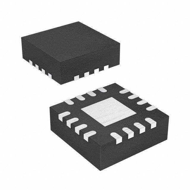
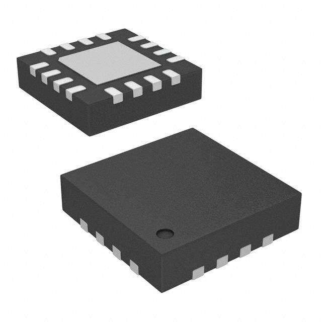
| 供应商器件封装 | 16-VQFN(4x4) |
| 其它名称 | 296-25327-2 |
| 制造商产品页 | http://www.ti.com/general/docs/suppproductinfo.tsp?distId=10&orderablePartNumber=CC2591RGVR |
| 包装 | 带卷 (TR) |
| 商标 | Texas Instruments |
| 噪声系数 | 4.8 dB |
| 安装风格 | SMD/SMT |
| 封装 | Reel |
| 封装/外壳 | 16-VQFN 裸露焊盘 |
| 封装/箱体 | VQFN-16 |
| 工作电源电压 | 2 V to 3.6 V |
| 工作频率 | 2.4 GHz |
| 工厂包装数量 | 2500 |
| 最大工作温度 | + 85 C |
| 最小工作温度 | - 40 C |
| 标准包装 | 2,500 |
| 特性 | - |
| 电源电流 | 3.4 mA |
| 类型 | 802.15.4, Zigbee |
| 系列 | CC2591 |
| 配用 | /product-detail/zh/CC2591EMK/296-24111-ND/1896371 |
| 频率 | 2.4GHz |

.jpg)


- 商务部:美国ITC正式对集成电路等产品启动337调查
- 曝三星4nm工艺存在良率问题 高通将骁龙8 Gen1或转产台积电
- 太阳诱电将投资9.5亿元在常州建新厂生产MLCC 预计2023年完工
- 英特尔发布欧洲新工厂建设计划 深化IDM 2.0 战略
- 台积电先进制程称霸业界 有大客户加持明年业绩稳了
- 达到5530亿美元!SIA预计今年全球半导体销售额将创下新高
- 英特尔拟将自动驾驶子公司Mobileye上市 估值或超500亿美元
- 三星加码芯片和SET,合并消费电子和移动部门,撤换高东真等 CEO
- 三星电子宣布重大人事变动 还合并消费电子和移动部门
- 海关总署:前11个月进口集成电路产品价值2.52万亿元 增长14.8%


PDF Datasheet 数据手册内容提取
Product Sample & Technical Tools & Support & Folder Buy Documents Software Community CC2591 SWRS070B–MARCH2008–REVISEDSEPTEMBER2014 CC2591 2.4-GHz RF Front End 1 Device Overview 1.1 Features 1 • SeamlessInterfaceto2.4-GHzLow-PowerRF • DigitalControlofLNAGainbyHGMPin DevicesfromTexasInstruments • 100-nAinPowerDown(EN=PAEN=0) • OutputPowerupto22dBm • LowTransmitCurrentConsumption • FewExternalComponents (100mAat3Vfor20-dBmOut,PAE=33%) – IntegratedSwitches • Low-ReceiveCurrentConsumption – IntegratedMatchingNetwork – 3.4mAforHigh-GainMode – IntegratedBalun – 1.7mAforLow-GainMode – IntegratedInductors • 4.8-dBLNANoiseFigure,IncludingT/RSwitch – IntegratedPA andExternalAntennaMatch – IntegratedLNA • RoHSCompliant4×4-mmQFN-16Package • 2-Vto3.6-VOperation 1.2 Applications • All2.4-GHzISMBandSystems • IEEE802.15.4andZigBee®Systems • WirelessSensorNetworks • WirelessConsumerSystems • WirelessIndustrialSystems • WirelessAudioSystems 1.3 Description CC2591 is a cost-effective and high-performance RF front end for low-power and low-voltage 2.4-GHz wireless applications. The device is a range extender for all existing and future 2.4-GHz low-power RF transceivers, transmitters, and System-on-Chip products from TI. CC2591 increases the link budget by providing a power amplifier for increased output power, and an LNA with low noise figure for improved receiver sensitivity. The device provides a small size, high output power RF design with its 4-mm × 4-mm QFN-16 package. The device contains PA, LNA, switches, RF-matching, and balun for simple design of high-performancewirelessapplications. DeviceInformation(1) PARTNUMBER PACKAGE BODYSIZE CC2591RGV RGV(16) 4.00mm×4.00mm (1) Formoreinformation,seeSection7,MechanicalPackagingandOrderableInformation. 1 AnIMPORTANTNOTICEattheendofthisdatasheetaddressesavailability,warranty,changes,useinsafety-criticalapplications, intellectualpropertymattersandotherimportantdisclaimers.PRODUCTIONDATA.
CC2591 SWRS070B–MARCH2008–REVISEDSEPTEMBER2014 www.ti.com 1.4 Functional Block Diagram Figure1-1showsthefunctionalblockdiagramofthedevice. PA BALUN 4 RF_P 11 ANT 3 RXTX LNA 2 RF_N Logic 5 PAEN Bias 6 EN 15 7 BIAS HGM Figure1-1.FunctionalBlockDiagram 2 DeviceOverview Copyright©2008–2014,TexasInstrumentsIncorporated SubmitDocumentationFeedback ProductFolderLinks:CC2591
CC2591 www.ti.com SWRS070B–MARCH2008–REVISEDSEPTEMBER2014 Table of Contents 1 DeviceOverview......................................... 1 4.6 Typical Characteristics............................... 8 1.1 Features.............................................. 1 5 Applications,Implementation,andLayout......... 9 ........................................... ....................... 1.2 Applications 1 5.1 CC2591EMEvaluationModule 9 ............................................ ........ 1.3 Description 1 5.2 ControllingtheOutputPowerfromCC2591 10 1.4 FunctionalBlockDiagram............................ 2 6 DeviceandDocumentationSupport............... 14 2 Revision History......................................... 3 6.1 DeviceSupport...................................... 14 3 TerminalConfigurationandFunctions.............. 4 6.2 DocumentationSupport............................. 15 ......................................... .......................................... 3.1 PinAttributes 5 6.3 Trademarks 15 4 Specifications ............................................ 6 6.4 ElectrostaticDischargeCaution..................... 16 .......................... ............................... 4.1 AbsoluteMaximumRatings 6 6.5 ExportControlNotice 16 ..................................... ............................................. 4.2 Handling Ratings 6 6.6 Glossary 16 4.3 RecommendedOperatingConditions................ 6 7 MechanicalPackagingandOrderable ............................. Information.............................................. 17 4.4 ElectricalCharacteristics 6 .............................. 4.5 ThermalResistanceCharacteristicsforRGV 7.1 PackagingInformation 17 .............................................. Package 7 2 Revision History NOTE:Pagenumbersforpreviousrevisionsmaydifferfrompagenumbersinthecurrentversion. ChangesfromRevisionA(June2008)toRevisionB Page • ChangedformatofdatasheettothelatestTIstandards........................................................................ 1 Copyright©2008–2014,TexasInstrumentsIncorporated RevisionHistory 3 SubmitDocumentationFeedback ProductFolderLinks:CC2591
CC2591 SWRS070B–MARCH2008–REVISEDSEPTEMBER2014 www.ti.com 3 Terminal Configuration and Functions TheCC2591pinoutanddescriptionareshowninFigure3-1andTable3-1,respectively. S A A N I B L _ _ D D D S D D V A N V A BI G A 16 15 14 13 AVDD_PA1 1 12 GND RF_N ANT 2 11 QFN-16 4x4mm RXTX 3 10 AVDD_PA2 RF_P GND 4 9 5 6 7 8 N N M D E E G N A H G P Figure3-1.PINANDI/OCONFIGURATION(TOPVIEW) NOTE The exposed die attach pad must be connected to a solid ground plane as this is the primarygroundconnectionforthechip.Inductanceinviastothepadshouldbeminimized.It ishighlyrecommendedtofollowthereferencelayout.Changeswillaltertheperformance. For best performance, minimize the length of the ground vias, by using a 4-layer PCB with groundplaneaslayer2whenCC2591ismountedontolayer1. 4 TerminalConfigurationandFunctions Copyright©2008–2014,TexasInstrumentsIncorporated SubmitDocumentationFeedback ProductFolderLinks:CC2591
CC2591 www.ti.com SWRS070B–MARCH2008–REVISEDSEPTEMBER2014 3.1 Pin Attributes Table3-1.PinAttributes TERMINAL TYPE DESCRIPTION NO. NAME Theexposeddieattachpadmustbeconnectedtoasolidgroundplane.See — GND Ground CC2591EMreferencedesignforrecommendedlayout. 1 2.0V–3.6VPower.PCBtracetothispinservesasinductiveloadtoPA.See AVDD_PA1 Power CC2591EMreferencedesignforrecommendedlayout. 2 RF_N RF RFinterfacetowardsCC24xxorCC25xxdevice. RXTXswitchingvoltagewhenconnectedtoCC24xxdevices.SeeTable5-2and 3 RXTX Analog/Control Table5-3fordetails. 4 RF_P RF RFinterfacetowardsCC24xxorCC25xxdevice 5 PAEN DigitalInput Digitalcontrolpin.SeeTable5-2andTable5-3fordetails. 6 EN DigitalInput Digitalcontrolpin.SeeTable5-2andTable5-3fordetails. Digitalcontrolpin. 7 HGM DigitalInput HGM=1→DeviceinHighGainMode HGM=0→DeviceinLowGainMode(RXonly) Secondarygroundconnections.Shouldbeshortedtothedieattachpadonthetop 8,9,12,14 GND Ground PCBlayer. 2.0V–3.6VPower.PCBtracetothispinservesasinductiveloadtoPA.See 10 AVDD_PA2 Power CC2591EMreferencedesignforrecommendedlayout. 11 ANT RF Antennainterface. 2V–3.6VPower.PCBtracetothispinservesasinductiveloadtoLNA.See 13 AVDD_LNA Power CC2591EMreferencedesignforrecommendedlayout. 15 BIAS Analog Biasinginput.ResistorbetweenthisnodeandgroundsetsbiascurrenttoPAs. 16 AVDD_BIAS Power 2V–3.6VPower. Copyright©2008–2014,TexasInstrumentsIncorporated TerminalConfigurationandFunctions 5 SubmitDocumentationFeedback ProductFolderLinks:CC2591
CC2591 SWRS070B–MARCH2008–REVISEDSEPTEMBER2014 www.ti.com 4 Specifications 4.1 Absolute Maximum Ratings(1)(2) Undernocircumstancesmusttheabsolutemaximumratingsbeviolated.Stressexceedingoneormoreofthelimitingvalues maycausepermanentdamagetothedevice. PARAMETER VALUE UNIT Supplyvoltage Allsupplypinsmusthavethesamevoltage –0.3to3.6 V Voltageonanydigitalpin –0.3toV +0.3,max3.6 DD InputRFlevel 10 dBm (1) Stressesbeyondthoselistedunderabsolutemaximumratingsmaycausepermanentdamagetothedevice.Thesearestressratings only,andfunctionaloperationofthedeviceattheseoranyotherconditionsbeyondthoseindicatedunderrecommendedoperating conditionsisnotimplied.Exposuretoabsolute-maximum-ratedconditionsforextendedperiodsmayaffectdevicereliability. (2) AllvoltagevaluesarewithrespecttoV ,unlessotherwisenoted. SS 4.2 Handling Ratings MIN MAX UNIT T Storagetemperaturerange –50 150 °C stg HumanBodyModel(HBM),perANSI/ESDA/JEDEC Electrostaticdischarge(ESD) JS001(1) –600 600 V V ESD performance: ChargedDeviceModel(CDM), perJESD22-C101(2) –500 500 V (1) JEDECdocumentJEP155statesthat500-VHBMallowssafemanufacturingwithastandardESDcontrolprocess. (2) JEDECdocumentJEP157statesthat250-VCDMallowssafemanufacturingwithastandardESDcontrolprocess. 4.3 Recommended Operating Conditions TheoperatingconditionsforCC2591arelistedbelow. PARAMETER MIN MAX UNIT Ambienttemperaturerange –40 85 °C Operatingsupplyvoltage 2 3.6 V Operatingfrequencyrange 2400 2483.5 MHz 4.4 Electrical Characteristics T =25°C,V =3V,f =2440MHz(unlessotherwisenoted).MeasuredonCC2591EMreferencedesignincludingexternal C DD RF matchingcomponents. PARAMETER TESTCONDITIONS MIN TYP MAX UNIT Receivecurrent,High-GainMode HGM=1 3.4 4 Receivecurrent,Low-GainMode HGM=0 1.7 2 mA Transmitcurrent P =0.5dBm 112 IN Transmitcurrent Noinputsignal 40 50 Power-downcurrent EN=PAEN=0 0.1 0.3 μA High-inputlevel(controlpins) EN,PAEN,HGM,RXTX 1.3 V DD V Low-inputlevel(controlpins) EN,PAEN,HGM,RXTX 0.3 Powerdown-Receivemodeswitching 12 μs time Powerdown-Transmitmodeswitching 1 μs time RFReceive Gain,High-GainMode HGM=1 11 dB Gain,Low-GainMode HGM=0 1 dB Gainvariation,2400–2483.5MHz,High- HGM=1 1.3 dB GainMode Gainvariation,2.0V–3.6V,High-Gain HGM=1 1.5 dB Mode 6 Specifications Copyright©2008–2014,TexasInstrumentsIncorporated SubmitDocumentationFeedback ProductFolderLinks:CC2591
CC2591 www.ti.com SWRS070B–MARCH2008–REVISEDSEPTEMBER2014 Electrical Characteristics (continued) T =25°C,V =3V,f =2440MHz(unlessotherwisenoted).MeasuredonCC2591EMreferencedesignincludingexternal C DD RF matchingcomponents. PARAMETER TESTCONDITIONS MIN TYP MAX UNIT Gainvariation,-40°C–85°C,High-Gain HGM=1 3 dB Mode HGM=1,includinginternalT/Rswitchandexternal Noisefigure,High-GainMode 4.8 dB antennamatch Input1-dBcompression,High-GainMode HGM=1 –17 dBm InputIP3,High-GainMode HGM=1 –2 dBm Inputreflectioncoefficient,S11 HGM=1,measuredatantennaport –11 dB RFTransmit Gain 22 dB Outputpower,P P =0.5dBm 20.6 dBm OUT IN Maximumoutputpower P =5dBm 22 dBm IN PowerAddedEfficiency,PAE P =0.5dBm 34% IN Output1-dBcompression 19 dBm OutputIP3 32 dBm Outputpowervariationoverfrequency 2400–2483.5MHz,P =0.5dBm 0.5 dB IN Outputpowervariationoverpowersupply 2V–3.6V,P =0.5dBm 3.5 dB IN Outputpowervariationovertemperature -40°C–85°C,P =0.5dBm 1.5 dB IN P =0.5dBm.Thesecondharmoniccanbereduced IN Secondharmonicpower tobelowregulatorylimitsbyusinganexternalLCfilter –15 dBm andantenna. P =0.5dBm.Thethirdharmoniccanbereducedto IN Thirdharmonicpower belowregulatorylimitsbyusinganexternalLCfilter –30 dBm andantenna. 4.5 Thermal Resistance Characteristics for RGV Package NAME DESCRIPTION °C/W(1) (2) AIRFLOW(m/s)(3) RΘ Junction-to-case(top) 52.8 0.00 JC-top RΘ Junction-to-board 20.4 0.00 JB RΘ Junction-to-freeair 41.9 0.00 JA Psi Junction-to-packagetop 1.4 0.00 JT Psi Junction-to-board 20.5 0.00 JB RΘ Junction-to-case(bottom) 8.3 0.00 JC-bottom (1) °C/W=degreesCelsiusperwatt. (2) ThesevaluesarebasedonaJEDEC-defined2S2Psystem(withtheexceptionoftheThetaJC[RΘ ]value,whichisbasedona JC JEDEC-defined1S0Psystem)andwillchangebasedonenvironmentaswellasapplication.Formoreinformation,seethese EIA/JEDECstandards: • JESD51-2,IntegratedCircuitsThermalTestMethodEnvironmentalConditions-NaturalConvection(StillAir) • JESD51-3,LowEffectiveThermalConductivityTestBoardforLeadedSurfaceMountPackages • JESD51-7,HighEffectiveThermalConductivityTestBoardforLeadedSurfaceMountPackages • JESD51-9,TestBoardsforAreaArraySurfaceMountPackageThermalMeasurements (3) m/s=meterspersecond. Copyright©2008–2014,TexasInstrumentsIncorporated Specifications 7 SubmitDocumentationFeedback ProductFolderLinks:CC2591
CC2591 SWRS070B–MARCH2008–REVISEDSEPTEMBER2014 www.ti.com 4.6 Typical Characteristics 12 5.4 13 11 5.3 12 11 10 HGM 5.2 HGM 10 9 5.1 9 8 5 dB 8 B Gain−d 67 NF HGM 44..89 Figu−re ain−dB 567 e G 5 4.7 ois 4 N 4 4.6 3 LGM 3 4.5 2 1 2 LGM 4.4 0 1 4.3 -1 0 4.2 -2 -40 -20 0 20 40 60 80 2400 2410 2420 2430 2440 2450 2460 2470 2480 f−Frequency−MHz T−Temperature−oC Figure4-1.LNAGainandNoiseFigurevsFrequency Figure4-2.LNAGainvsTemperature 12 11 10 HGM 9 8 B 7 d − 6 n Gai 5 4 3 2 LGM 1 0 -1 2 2.2 2.4 2.6 2.8 3 3.2 3.4 3.6 Power Supply−V Figure4-3.LNAGainvsPowerSupply 8 Specifications Copyright©2008–2014,TexasInstrumentsIncorporated SubmitDocumentationFeedback ProductFolderLinks:CC2591
CC2591 www.ti.com SWRS070B–MARCH2008–REVISEDSEPTEMBER2014 5 Applications, Implementation, and Layout NOTE Information in the following applications sections is not part of the TI component specification, and TI does not warrant its accuracy or completeness. TI’s customers are responsible for determining suitability of components for their purposes. Customers should validateandtesttheirdesignimplementationtoconfirmsystemfunctionality. 5.1 CC2591EM Evaluation Module VDD VDD C11/C12 C101/C102 =TLINEinductor VDD VDD C161 C131/C132 TL11 TL101 TL131 S 1 2 A A A A N AVDD_BI AVDD_P AVDD_P AVDD_L RRRFFF___PPP LDB182G4520C-110 SMA RRXRXXTTTXXX Balun C2 SMA L111 L112 ANT CC2591 RRFRFF___NNN C111 PAEN PAEN EN EN S HGM HGM A BI RXTX R151 Figure5-1.CC2591EMEvaluationModule Copyright©2008–2014,TexasInstrumentsIncorporated Applications,Implementation,andLayout 9 SubmitDocumentationFeedback ProductFolderLinks:CC2591
CC2591 SWRS070B–MARCH2008–REVISEDSEPTEMBER2014 www.ti.com Table5-1.ListofMaterials(SeeCC2591EMReferenceDesign) DEVICE FUNCTION VALUE L112 Partofantennamatch. 1.5nH:LQW15AN1N5B00fromMurata L111 DCblock. 1nF:GRM1555C1H102JA01fromMurata C111 Partofantennamatch. 1pF:GRM1555C1H1R0BZ01fromMurata C161 Decouplingcapacitor. 1nF:GRM1555C1H102JA01fromMurata 10pF||1nF.Thesmallestcapclosest.SeeCC2591EM referencedesign(SWRU190)forplacement. C11/C12 Decoupling.WillaffectPAresonance. 10pF:GRM1555C1H100JZ01fromMurata 1nF:GRM1555C1H102JA01fromMurata 18pF||1nF.Thesmallestcapclosest.SeeCC2591EM referencedesign(SWRU190)forplacement. C101/C102 Decoupling.WillaffectPAresonance. 18pF:GRM1555C1H180JZ01fromMurata 1nF:GRM1555C1H102JA01fromMurata 10pF||1nF.Thesmallestcapclosest.SeeCC2591EM referencedesign(SWRU190)forplacement. C131/C132 Decoupling.WillaffectPAresonance. 10pF:GRM1555C1H100JZ01fromMurata 1nF:GRM1555C1H102JA01fromMurata C2 Decouplingofexternalbalun 1nF:GRM1555C1H102JA01fromMurata TL11 Transmissionline.WillaffectPAresonance. SeeCC2591EMreferencedesign. TL101 Transmissionline.WillaffectPAresonance. SeeCC2591EMreferencedesign. TL131 Transmissionline.WillaffectLNAresonance. SeeCC2591EMreferencedesign. R151 Biasresistor 4.3kΩ:RK73H1ETTP4301FfromKoa 5.2 Controlling the Output Power from CC2591 The output power of CC2591 is controlled by controlling the input power. The CC2591 PA is designed to workincompression(classAB),andthebestefficiencyisreachedwhenastronginputsignalisapplied. 5.2.1 Input Levels on Control Pins The four digital control pins (PAEN, EN, HGM, RXTX) have built-in level-shifting functionality, meaning that if the CC2591 is operating from a 3.6-V supply voltage, the control pins will still sense 1.6-V - 1.8-V signalsaslogical‘1’. An example of the above would be that RXTX is connected directly to the RXTX pin on CC24xx, but the global supply voltage is 3.6 V. The RXTX pin on CC24xx will switch between 0 V (RX) and 1.8 V(TX), whichisstillahighenoughvoltagetocontrolthemodeofCC2591. Theinputvoltagesshouldhowevernothavelogical ‘1’levelthatishigherthanthesupply. 5.2.2 Connecting CC2591 to a CC24xx Device Table5-2.ControlLogicforConnectingCC2591toaCC24xxDevice PAEN=EN RXTX HGM MODEOFOPERATION 0 X X PowerDown 1 0 0 RXLowGainMode 1 0 1 RXHighGainMode 1 1 X TX 10 Applications,Implementation,andLayout Copyright©2008–2014,TexasInstrumentsIncorporated SubmitDocumentationFeedback ProductFolderLinks:CC2591
CC2591 www.ti.com SWRS070B–MARCH2008–REVISEDSEPTEMBER2014 VDD VDD C11/C12 C101/C102 =TLINEinductor VDD VDD C161 C131/C132 TL11 TL101 TL131 CC243x S 1 2 A A A A N AVDD_BI AVDD_P AVDD_P AVDD_L RFRRFF___PPP RF_P RXRRXXTTTXXX TXRX_SWITCH C112 L111 CC2591 RRFRFF___NNN RF_N ANT PAEN L112 C113 C111 RREG_OUT(CC243x) EN S HGM A BI R151 Connectedto Alternativiely VDD/GND/MCU/RXTX fromMCU Figure5-2.CC2591+CC24xxApplicationCircuit Copyright©2008–2014,TexasInstrumentsIncorporated Applications,Implementation,andLayout 11 SubmitDocumentationFeedback ProductFolderLinks:CC2591
CC2591 SWRS070B–MARCH2008–REVISEDSEPTEMBER2014 www.ti.com 5.2.3 Connecting CC2591 to the CC2500, CC2510, or CC2511 Device Table5-3.ControlLogicforConnectingCC2591toaCC2500/10/11Devices PAEN EN RXTX HGM MODEOFOPERATION 0 0 NC X PowerDown 0 1 NC 0 RXLGM 0 1 NC 1 RXHGM 1 0 NC X TX 1 1 NC X Notallowed VDD VDD C11/C12 C101/C102 =TLINEinductor VDD VDD C161 C131/C132 TL11 TL101 TL131 CC2500 CC2510 S 1 2 A CC2511 A A A N AVDD_BI AVDD_P AVDD_P AVDD_L RRRFFF___PPP RF_P RRXRXXTTTXXX NC C112 L111 CC2591 ANT RRFRFF___NNN RF_N PAEN GDO0 L112 C113 C111 EN GDO2 S HGM A BI R151 Alternatively Connectedto fromMCU VDD/GND/MCU Figure5-3.CC2591+CC2500/10/11DeviceApplicationCircuit 12 Applications,Implementation,andLayout Copyright©2008–2014,TexasInstrumentsIncorporated SubmitDocumentationFeedback ProductFolderLinks:CC2591
CC2591 www.ti.com SWRS070B–MARCH2008–REVISEDSEPTEMBER2014 5.2.4 Connecting CC2591 to a CC2520 Device Table5-4.ControlLogicforConnectingCC2591toaCC2520Device PAEN EN RXTX HGM MODEOFOPERATION 0 0 NC X PowerDown 0 1 NC 0 RXLGM 0 1 NC 1 RXHGM 1 0 NC X TX 1 1 NC X Notallowed VDD VDD C11/C12 C101/C102 =TLINEinductor VDD VDD C161 C131/C132 TL11 TL101 TL131 CC2520 S 1 2 A A A A N AVDD_BI AVDD_P AVDD_P AVDD_L RRRFFF___PPP L41 C41 RF_P RRXRXXTTTXXX NC C1 C112 L111 ANT CC2591 RRFRFF___NNN L21 RF_N L112 C113 C111 PAEN PA_EN EN LNA_EN AS HGM C21 BI R151 Alternatively Connectedto fromMCU VDD/GND/MCU Figure5-4.CC2591+CC2520ApplicationCircuit Copyright©2008–2014,TexasInstrumentsIncorporated Applications,Implementation,andLayout 13 SubmitDocumentationFeedback ProductFolderLinks:CC2591
CC2591 SWRS070B–MARCH2008–REVISEDSEPTEMBER2014 www.ti.com 6 Device and Documentation Support 6.1 Device Support 6.1.1 Development Support TI offers an extensive line of development tools, including tools to evaluate the performance of the processors, generate code, develop algorithm implementations, and fully integrate and debug software and hardware modules. The tool's support documentation is electronically available within the Code ComposerStudio™IntegratedDevelopmentEnvironment(IDE). ThefollowingproductssupportdevelopmentoftheCC2591deviceapplications: Software Development Tools: Code Composer Studio™ Integrated Development Environment (IDE): including Editor C/C++/Assembly Code Generation, and Debug plus additional development tools Scalable, Real-Time Foundation Software (DSP/BIOS™), which provides the basic run-time target softwareneededtosupportanyCC2591deviceapplication. HardwareDevelopmentTools: ExtendedDevelopmentSystem(XDS™)Emulator For a complete listing of development-support tools for the CC2591 platform, visit the Texas Instruments website at www.ti.com. For information on pricing and availability, contact the nearest TI field sales office orauthorizeddistributor. 6.1.2 Device Nomenclature To designate the stages in the product development cycle, TI assigns prefixes to the part numbers of all microprocessors (MPUs) and support tools. Each device has one of three prefixes: X, P, or null (no prefix) (for example, CC2591). These prefixes represent evolutionary stages of product development from engineeringprototypes(TMDX)throughfullyqualifiedproductiondevicesandtools(TMDS). Devicedevelopmentevolutionaryflow: X Experimental device that is not necessarily representative of the final device's electrical specificationsandmaynotuseproductionassemblyflow. P Prototype device that is not necessarily the final silicon die and may not necessarily meet finalelectricalspecifications. null Productionversionofthesilicondiethatisfullyqualified. Supporttooldevelopmentevolutionaryflow: XandPdevicesareshippedagainstthefollowingdisclaimer: "Developmentalproductisintendedforinternalevaluationpurposes." Production devices have been characterized fully, and the quality and reliability of the device have been demonstratedfully.TI'sstandardwarrantyapplies. Predictions show that prototype devices (X or P) have a greater failure rate than the standard production devices. Texas Instruments recommends that these devices not be used in any production system because their expected end-use failure rate still is undefined. Only qualified production devices are to be used. TI device nomenclature also includes a suffix with the device family name. This suffix indicates the package type (for example, RGV) and the temperature range (for example, blank is the default commercial temperature range). provides a legend for reading the complete device name for any CC2591 device. For orderable part numbers of CC2591 devices in the RGV package types, see the Package Option Addendumofthisdocument,theTIwebsite(www.ti.com),orcontactyourTIsalesrepresentative. 14 DeviceandDocumentationSupport Copyright©2008–2014,TexasInstrumentsIncorporated SubmitDocumentationFeedback ProductFolderLinks:CC2591
CC2591 www.ti.com SWRS070B–MARCH2008–REVISEDSEPTEMBER2014 6.2 Documentation Support ThefollowingdocumentsdescribetheCC2591processor.Copiesofthesedocumentsareavailableonthe Internetatwww.ti.com. SWRA351 AntennaQuickGuide SWRA120 DesignNoteOverview SWRA350 YAGI2.4GHzPCBAntenna SWRA161 AntennaSelectionGuide SWRA328 CC-Antenna-DKDocumentationandAntennaMeasurementsSummary SWRA229 UsingCC2591RFFrontEndwithCC2520 SWRA308 UsingCC2591FrontEndwithCC2530andCC2531 SWRA290 TIMACandZ-StackModificationsforusingCC2591RFFrontEndwithCC2 SWRA236 DesignStepsandResultsforChangingPCBLayerThickness SWRA230 TI-MACmodificationsforusingCC2591PA/LNAwithMSP430F2618+CC2520 SWRA208 TI-MACandZ-StackmodificationsforusingCC2591RFFrontEndw/CC2430 SWRA212 UsingCC2591RFFrontEndwithCC2430 SWRC171 CC2530-CC2591EMReferenceDesign SPRU137 CC2520SoftwareExamplesUser'sGuide SPRU178 CC2430SoftwareExamplesUser’sGuide 6.2.1 Community Resources The following links connect to TI community resources. Linked contents are provided "AS IS" by the respective contributors. They do not constitute TI specifications and do not necessarily reflect TI's views; seeTI'sTermsofUse. TIE2E™OnlineCommunity TI's Engineer-to-Engineer (E2E) Community. Created to foster collaboration among engineers. At e2e.ti.com, you can ask questions, share knowledge, exploreideasandhelpsolveproblemswithfellowengineers. TIEmbeddedProcessorsWiki Texas Instruments Embedded Processors Wiki. Established to help developers get started with Embedded Processors from Texas Instruments and to foster innovation and growth of general knowledge about the hardware and software surrounding thesedevices. 6.3 Trademarks E2EisatrademarkofTexasInstruments. ZigBeeisaregisteredtrademarkofZigBeeAlliance. Copyright©2008–2014,TexasInstrumentsIncorporated DeviceandDocumentationSupport 15 SubmitDocumentationFeedback ProductFolderLinks:CC2591
CC2591 SWRS070B–MARCH2008–REVISEDSEPTEMBER2014 www.ti.com 6.4 Electrostatic Discharge Caution This integrated circuit can be damaged by ESD. Texas Instruments recommends that all integrated circuits be handled with appropriateprecautions.Failuretoobserveproperhandlingandinstallationprocedurescancausedamage. ESDdamagecanrangefromsubtleperformancedegradationtocompletedevicefailure.Precisionintegratedcircuitsmaybemore susceptibletodamagebecauseverysmallparametricchangescouldcausethedevicenottomeetitspublishedspecifications. 6.5 Export Control Notice Recipient agrees to not knowingly export or re-export, directly or indirectly, any product or technical data (as defined by the U.S., EU, and other Export Administration Regulations) including software, or any controlled product restricted by other applicable national regulations, received from disclosing party under nondisclosure obligations (if any), or any direct product of such technology, to any destination to which such export or re-export is restricted or prohibited by U.S. or other applicable laws, without obtaining prior authorization from U.S. Department of Commerce and other competent Government authorities to the extentrequiredbythoselaws. 6.6 Glossary SLYZ022—TIGlossary. Thisglossarylistsandexplainsterms,acronyms,anddefinitions. 16 DeviceandDocumentationSupport Copyright©2008–2014,TexasInstrumentsIncorporated SubmitDocumentationFeedback ProductFolderLinks:CC2591
CC2591 www.ti.com SWRS070B–MARCH2008–REVISEDSEPTEMBER2014 7 Mechanical Packaging and Orderable Information 7.1 Packaging Information The following pages include mechanical packaging and orderable information. This information is the most current data available for the designated devices. This data is subject to change without notice and revisionofthisdocument.Forbrowser-basedversionsofthisdatasheet,refertotheleft-handnavigation. Copyright©2008–2014,TexasInstrumentsIncorporated MechanicalPackagingandOrderableInformation 17 SubmitDocumentationFeedback ProductFolderLinks:CC2591
PACKAGE OPTION ADDENDUM www.ti.com 24-Aug-2018 PACKAGING INFORMATION Orderable Device Status Package Type Package Pins Package Eco Plan Lead/Ball Finish MSL Peak Temp Op Temp (°C) Device Marking Samples (1) Drawing Qty (2) (6) (3) (4/5) CC2591RGVR NRND VQFN RGV 16 2500 Green (RoHS CU NIPDAU Level-2-260C-1 YEAR -40 to 85 CC2591 & no Sb/Br) CC2591RGVRG4 NRND VQFN RGV 16 2500 Green (RoHS CU NIPDAU Level-2-260C-1 YEAR -40 to 85 CC2591 & no Sb/Br) CC2591RGVT NRND VQFN RGV 16 250 Green (RoHS CU NIPDAU Level-2-260C-1 YEAR -40 to 85 CC2591 & no Sb/Br) CC2591RGVTG4 NRND VQFN RGV 16 250 Green (RoHS CU NIPDAU Level-2-260C-1 YEAR -40 to 85 CC2591 & no Sb/Br) HPA00420RGVR NRND VQFN RGV 16 2500 Green (RoHS CU NIPDAU Level-2-260C-1 YEAR -40 to 85 CC2591 & no Sb/Br) HPA01083RGVR NRND VQFN RGV 16 2500 Green (RoHS CU NIPDAU Level-2-260C-1 YEAR -40 to 85 CC2591 & no Sb/Br) (1) The marketing status values are defined as follows: ACTIVE: Product device recommended for new designs. LIFEBUY: TI has announced that the device will be discontinued, and a lifetime-buy period is in effect. NRND: Not recommended for new designs. Device is in production to support existing customers, but TI does not recommend using this part in a new design. PREVIEW: Device has been announced but is not in production. Samples may or may not be available. OBSOLETE: TI has discontinued the production of the device. (2) RoHS: TI defines "RoHS" to mean semiconductor products that are compliant with the current EU RoHS requirements for all 10 RoHS substances, including the requirement that RoHS substance do not exceed 0.1% by weight in homogeneous materials. Where designed to be soldered at high temperatures, "RoHS" products are suitable for use in specified lead-free processes. TI may reference these types of products as "Pb-Free". RoHS Exempt: TI defines "RoHS Exempt" to mean products that contain lead but are compliant with EU RoHS pursuant to a specific EU RoHS exemption. Green: TI defines "Green" to mean the content of Chlorine (Cl) and Bromine (Br) based flame retardants meet JS709B low halogen requirements of <=1000ppm threshold. Antimony trioxide based flame retardants must also meet the <=1000ppm threshold requirement. (3) MSL, Peak Temp. - The Moisture Sensitivity Level rating according to the JEDEC industry standard classifications, and peak solder temperature. (4) There may be additional marking, which relates to the logo, the lot trace code information, or the environmental category on the device. (5) Multiple Device Markings will be inside parentheses. Only one Device Marking contained in parentheses and separated by a "~" will appear on a device. If a line is indented then it is a continuation of the previous line and the two combined represent the entire Device Marking for that device. Addendum-Page 1
PACKAGE OPTION ADDENDUM www.ti.com 24-Aug-2018 (6) Lead/Ball Finish - Orderable Devices may have multiple material finish options. Finish options are separated by a vertical ruled line. Lead/Ball Finish values may wrap to two lines if the finish value exceeds the maximum column width. Important Information and Disclaimer:The information provided on this page represents TI's knowledge and belief as of the date that it is provided. TI bases its knowledge and belief on information provided by third parties, and makes no representation or warranty as to the accuracy of such information. Efforts are underway to better integrate information from third parties. TI has taken and continues to take reasonable steps to provide representative and accurate information but may not have conducted destructive testing or chemical analysis on incoming materials and chemicals. TI and TI suppliers consider certain information to be proprietary, and thus CAS numbers and other limited information may not be available for release. In no event shall TI's liability arising out of such information exceed the total purchase price of the TI part(s) at issue in this document sold by TI to Customer on an annual basis. Addendum-Page 2
PACKAGE MATERIALS INFORMATION www.ti.com 26-Feb-2019 TAPE AND REEL INFORMATION *Alldimensionsarenominal Device Package Package Pins SPQ Reel Reel A0 B0 K0 P1 W Pin1 Type Drawing Diameter Width (mm) (mm) (mm) (mm) (mm) Quadrant (mm) W1(mm) CC2591RGVR VQFN RGV 16 2500 330.0 12.4 4.3 4.3 1.5 8.0 12.0 Q2 CC2591RGVT VQFN RGV 16 250 180.0 12.4 4.3 4.3 1.5 8.0 12.0 Q2 PackMaterials-Page1
PACKAGE MATERIALS INFORMATION www.ti.com 26-Feb-2019 *Alldimensionsarenominal Device PackageType PackageDrawing Pins SPQ Length(mm) Width(mm) Height(mm) CC2591RGVR VQFN RGV 16 2500 350.0 350.0 43.0 CC2591RGVT VQFN RGV 16 250 210.0 185.0 35.0 PackMaterials-Page2
None
None
None
IMPORTANTNOTICEANDDISCLAIMER TIPROVIDESTECHNICALANDRELIABILITYDATA(INCLUDINGDATASHEETS),DESIGNRESOURCES(INCLUDINGREFERENCE DESIGNS),APPLICATIONOROTHERDESIGNADVICE,WEBTOOLS,SAFETYINFORMATION,ANDOTHERRESOURCES“ASIS” ANDWITHALLFAULTS,ANDDISCLAIMSALLWARRANTIES,EXPRESSANDIMPLIED,INCLUDINGWITHOUTLIMITATIONANY IMPLIEDWARRANTIESOFMERCHANTABILITY,FITNESSFORAPARTICULARPURPOSEORNON-INFRINGEMENTOFTHIRD PARTYINTELLECTUALPROPERTYRIGHTS. TheseresourcesareintendedforskilleddevelopersdesigningwithTIproducts.Youaresolelyresponsiblefor(1)selectingtheappropriate TIproductsforyourapplication,(2)designing,validatingandtestingyourapplication,and(3)ensuringyourapplicationmeetsapplicable standards,andanyothersafety,security,orotherrequirements.Theseresourcesaresubjecttochangewithoutnotice.TIgrantsyou permissiontousetheseresourcesonlyfordevelopmentofanapplicationthatusestheTIproductsdescribedintheresource.Other reproductionanddisplayoftheseresourcesisprohibited.NolicenseisgrantedtoanyotherTIintellectualpropertyrightortoanythird partyintellectualpropertyright.TIdisclaimsresponsibilityfor,andyouwillfullyindemnifyTIanditsrepresentativesagainst,anyclaims, damages,costs,losses,andliabilitiesarisingoutofyouruseoftheseresources. TI’sproductsareprovidedsubjecttoTI’sTermsofSale(www.ti.com/legal/termsofsale.html)orotherapplicabletermsavailableeitheron ti.comorprovidedinconjunctionwithsuchTIproducts.TI’sprovisionoftheseresourcesdoesnotexpandorotherwisealterTI’sapplicable warrantiesorwarrantydisclaimersforTIproducts. MailingAddress:TexasInstruments,PostOfficeBox655303,Dallas,Texas75265 Copyright©2019,TexasInstrumentsIncorporated