ICGOO在线商城 > 射频/IF 和 RFID > RF 前端(LNA + PA) > AD9863BCPZ-50
 Datasheet下载
- 型号: AD9863BCPZ-50
- 制造商: Analog
- 库位|库存: xxxx|xxxx
- 要求:
| 数量阶梯 | 香港交货 | 国内含税 |
| +xxxx | $xxxx | ¥xxxx |
查看当月历史价格
查看今年历史价格
AD9863BCPZ-50产品简介:
ICGOO电子元器件商城为您提供AD9863BCPZ-50由Analog设计生产,在icgoo商城现货销售,并且可以通过原厂、代理商等渠道进行代购。 AD9863BCPZ-50价格参考¥188.88-¥188.88。AnalogAD9863BCPZ-50封装/规格:RF 前端(LNA + PA), RF Front End WLL,WLAN 64-LFCSP-VQ(9x9)。您可以下载AD9863BCPZ-50参考资料、Datasheet数据手册功能说明书,资料中有AD9863BCPZ-50 详细功能的应用电路图电压和使用方法及教程。
AD9863BCPZ-50 是由 Analog Devices Inc.(ADI)公司推出的一款高性能射频前端器件,集成了低噪声放大器(LNA)和功率放大器(PA),适用于多种无线通信应用。

该器件主要应用于无线基站、无线接入系统、点对点微波通信、蜂窝通信系统(如GSM、CDMA、WCDMA)、WiMAX 和 LTE 基站等射频通信设备中。其高集成度设计有助于减少电路板空间,提高系统可靠性。

AD9863BCPZ-50 支持宽频带工作,适用于多频段和多标准无线设备。其内部的LNA具有低噪声系数和高增益,有助于提升接收机的灵敏度;而PA则提供较高的输出功率和良好的效率,适合用于发射通道的信号放大。

此外,该芯片也可用于测试设备、工业控制、军事通信和广播系统等对射频性能要求较高的场合。

总之,AD9863BCPZ-50 凭借其高性能和集成化设计,广泛应用于现代通信系统中的射频前端模块,尤其适合对尺寸和性能有较高要求的无线基础设施设备。
| 参数 | 数值 |
| 产品目录 | |
| 描述 | IC FRONT-END MIXED-SGNL 64-LFCSP模数转换器 - ADC 12-Bit Mixed-Signal Front-End Processor |
| 产品分类 | RF 前端 (LNA + PA)集成电路 - IC |
| 品牌 | Analog Devices |
| 产品手册 | |
| 产品图片 |
|
| rohs | 符合RoHS无铅 / 符合限制有害物质指令(RoHS)规范要求 |
| 产品系列 | 数据转换器IC,模数转换器 - ADC,Analog Devices AD9863BCPZ-50- |
| 数据手册 | |
| 产品型号 | AD9863BCPZ-50 |
| RF类型 | WLL,WLAN |
| 产品目录页面 | |
| 产品种类 | 模数转换器 - ADC |
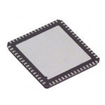
| 供应商器件封装 | 64-LFCSP-VQ(9x9) |
| 信噪比 | 67 dB |
| 其它名称 | AD9863BCPZ50 |
| 分辨率 | 12 bit |
| 包装 | 托盘 |
| 商标 | Analog Devices |
| 安装风格 | SMD/SMT |
| 封装 | Tray |
| 封装/外壳 | 64-VFQFN 裸露焊盘,CSP |
| 封装/箱体 | LFCSP-64 |
| 工作电源电压 | 3.3 V |
| 工厂包装数量 | 260 |
| 最大工作温度 | + 85 C |
| 最小工作温度 | - 40 C |
| 标准包装 | 1 |
| 特性 | 12 位 ADC,12 位 DAC |
| 电压参考 | Internal, External |
| 系列 | AD9863 |
| 结构 | Pipeline |
| 视频文件 | http://www.digikey.cn/classic/video.aspx?PlayerID=1364138032001&width=640&height=505&videoID=2245193150001 |
| 转换速率 | 50 MS/s |
| 输入类型 | Differential |
| 通道数量 | 2 Channel |
| 频率 | - |


- 商务部:美国ITC正式对集成电路等产品启动337调查
- 曝三星4nm工艺存在良率问题 高通将骁龙8 Gen1或转产台积电
- 太阳诱电将投资9.5亿元在常州建新厂生产MLCC 预计2023年完工
- 英特尔发布欧洲新工厂建设计划 深化IDM 2.0 战略
- 台积电先进制程称霸业界 有大客户加持明年业绩稳了
- 达到5530亿美元!SIA预计今年全球半导体销售额将创下新高
- 英特尔拟将自动驾驶子公司Mobileye上市 估值或超500亿美元
- 三星加码芯片和SET,合并消费电子和移动部门,撤换高东真等 CEO
- 三星电子宣布重大人事变动 还合并消费电子和移动部门
- 海关总署:前11个月进口集成电路产品价值2.52万亿元 增长14.8%

PDF Datasheet 数据手册内容提取
Mixed-Signal Front-End (MxFE™) Baseband Transceiver for Broadband Applications Data Sheet AD9863 FEATURES FUNCTIONAL BLOCK DIAGRAM Receive path includes dual 12-bit, 50 MSPS analog-to-digital VIN+A converters with internal or external reference Transmit path includes dual 12-bit, 200 MSPS digital-to- VIN–A ADC DMAUTXA Rx DATA VIN+B AND analog converters with 1×, 2×, or 4× interpolation and ADC LATCH VIN–B programmable gain control I/O Internal clock distribution block includes a programmable I/O ICNOTNETRRFOACLE INTERFACE phase-locked loop and timing generation circuitry, LOW-PASS CONFIGURATION FLEXIBLE INTERPOLATION BLOCK I/O BUS allowing single-reference clock operation FILTER [0:23] IOUT+A 24-pin flexible I/O data interface allows various interleaved DAC DATA or noninterleaved data transfers in half-duplex mode and IOUT–A LATCH AND interleaved data transfers in full-duplex mode IOUT+B DEMUX Tx DATA DAC Configurable through register programmability or IOUT–B optionally limited programmability through mode pins ADC CLOCK CLKIN1 CLOCK Independent Rx and Tx power-down control pins GENERATION 64-lead LFCSP package (9 mm × 9 mm footprint) DAC CLOCK BLOCK PLL CLKIN2 APPLICATIONS AD9863 03604-0-070 Broadband access Figure 1. Broadband LAN Communications (modems) GENERAL DESCRIPTION The AD9863 is a member of the MxFE family—a group of In half-duplex systems, the interface supports 24-bit parallel integrated converters for the communications market. The transfers or 12-bit interleaved transfers. In full-duplex systems, AD9863 integrates dual 12-bit analog-to-digital converters the interface supports a 12-bit interleaved ADC bus and a (ADC) and dual 12-bit digital-to-analog converters (TxDAC®). 12-bit interleaved TxDAC bus. The flexible I/O bus reduces pin The AD9863 ADCs are optimized for ADC sampling of 50 MSPS count, also reducing the required package size on the AD9863 and less. The dual TxDACs operate at speeds up to 200 MHz and the device to which it connects. and include a bypassable 2× or 4× interpolation filter. The The AD9863 can use either mode pins or a serial programma- AD9863 is optimized for high performance, low power, and ble interface (SPI) to configure the interface bus, operate the small form factor to provide a cost-effective solution for the ADC in a low power mode, configure the TxDAC interpolation broadband communications market. rate, and control ADC and TxDAC power-down. The SPI The AD9863 uses a single input clock pin (CLKIN) or two provides more programmable options for both the TxDAC path independent clocks for the Tx path and the Rx path. The ADC (for example, coarse and fine gain control and offset control for and TxDAC clocks are generated within a timing generation channel matching) and the ADC path (for example, the internal block that provides user programmable options such as divide duty cycle stabilizer and twos complement data format). circuits, PLL multipliers, and switches. The AD9863 is packaged in a 64-lead LFCSP (low profile, fine A flexible, bidirectional 24-bit I/O bus accommodates a variety pitched, chip scale package). The 64-lead LFCSP footprint is of custom digital back ends or open market DSPs. only 9 mm × 9 mm and is less than 0.9 mm high, fitting into such tightly spaced applications as PCMCIA cards. Rev. B Document Feedback Information furnished by Analog Devices is believed to be accurate and reliable. However, no responsibility is assumed by Analog Devices for its use, nor for any infringements of patents or other One Technology Way, P.O. Box 9106, Norwood, MA 02062-9106, U.S.A. rights of third parties that may result from its use. Specifications subject to change without notice. No license is granted by implication or otherwise under any patent or patent rights of Analog Devices. Tel: 781.329.4700 ©2003–2017 Analog Devices, Inc. All rights reserved. Trademarks and registered trademarks are the property of their respective owners. Technical Support www.analog.com
AD9863 Data Sheet TABLE OF CONTENTS Features .............................................................................................. 1 Pin Configuration and Function Descriptions ..............................8 Applications ....................................................................................... 1 Typical Performance Characteristics ........................................... 10 Functional Block Diagram .............................................................. 1 Terminology .................................................................................... 17 General Description ......................................................................... 1 Theory of Operation ...................................................................... 18 Revision History ........................................................................... 2 System Block ............................................................................... 18 Tx Path Specifications ...................................................................... 3 Rx Path Block .............................................................................. 18 Rx Path Specifications ...................................................................... 4 Tx Path Block .............................................................................. 20 Power Specifications ......................................................................... 5 Digital Block................................................................................ 23 Digital Specifications ........................................................................ 5 Programmable Registers ............................................................ 33 Timing Specifications ....................................................................... 6 Clock Distribution Block .......................................................... 36 Absolute Maximum Ratings ............................................................ 7 Outline Dimensions ....................................................................... 40 Thermal Resistance ...................................................................... 7 Ordering Guide .......................................................................... 40 ESD Caution .................................................................................. 7 REVISION HISTORY 4/2017—Rev. A to Rev. B Changes to Figure 3 and Table 8 ..................................................... 8 Updated Outline Dimensions ....................................................... 42 Changes to Ordering Guide .......................................................... 42 4/2005—Rev. 0 to Rev. A Changes to Ordering Guide .......................................................... 40 11/2003—Revision 0: Initial Version Rev. B | Page 2 of 40
Data Sheet AD9863 Tx PATH SPECIFICATIONS FDAC = 200 MSPS; 4× interpolation; RSET = 4.02 kΩ; differential load resistance of 100 Ω1; TxPGA = 20 dB; AVDD = DVDD = 3.3 V, unless otherwise noted. Table 1. Parameter Temp Test Level Min Typ Max Unit Tx PATH GENERAL Resolution Full IV 12 Bits Maximum DAC Update Rate Full IV 200 MHz Maximum Full-Scale Output Current Full IV 20 mA Full-Scale Error Full V 1% Gain Mismatch Error 25°C IV −3.5 +3.5 % FS Offset Mismatch Error Full IV −0.1 +0.1 % FS Reference Voltage Full V 1.23 V Output Capacitance Full V 5 pF Phase Noise (1 kHz Offset, 6 MHz Tone) 25°C V −115 dBc/Hz Output Voltage Compliance Range Full IV −1.0 +1.0 V TxPGA Gain Range Full V 20 dB TxPGA Step Size Full V 0.10 dB Tx PATH DYNAMIC PERFORMANCE (I = 20 mA; F = 1 MHz) OUTFS OUT SNR Full IV 70.8 71.6 dB SINAD Full IV 64.3 71 dB THD Full IV −79 −66.3 dBc SFDR, Wide Band (DC to Nyquist) Full IV 68.5 77 dBc SFDR, Narrow Band (1 MHz Window) Full IV 72.8 81 dBc 1 See Figure 2 for description of the TxDAC termination scheme. TxDAC 50 50 03604-0-071 Figure 2. Diagram Showing Termination of 100 Ω Differential Load for Some TxDAC Measurements Rev. B | Page 3 of 40
AD9863 Data Sheet RX PATH SPECIFICATIONS F = 50 MSPS; internal reference; differential analog inputs, ADC_AVDD = DVDD = 3.3 V, unless otherwise noted. ADC Table 2. Parameter Temp Test Level Min Typ Max Unit Rx PATH GENERAL Resolution Full V 12 Bits Maximum ADC Sample Rate Full IV 50 MSPS Gain Mismatch Error Full V ±0.2 % FS Offset Mismatch Error Full V ±0.1 % FS Reference Voltage Full V 1.0 V Reference Voltage (REFT–REFB) Error Full IV −30 ±6 +30 mV Input Resistance (Differential) Full V 2 kΩ Input Capacitance Full V 5 pF Input Bandwidth Full V 30 MHz Differential Analog Input Voltage Range Full V 2 V p-p differential Rx PATH DC ACCURACY Integral Nonlinearity (INL) 25°C V ±0.75 LSB Differential Nonlinearity (DNL) 25°C V ±0.75 LSB Aperture Delay 25°C V 2.0 ns Aperture Uncertainty (Jitter) 25°C V 1.2 ps rms Input Referred Noise 25°C V 250 µV AD9863 Rx PATH DYNAMIC PERFORMANCE (V = –0.5 dBFS; F = 10 MHz) IN IN SNR Full V 67 dBc SINAD Full V 65.5 dBc THD (Second to Ninth Harmonics) Full IV −73 −66.6 dBc SFDR, Wide Band (DC to Nyquist) Full IV 68.3 74 dBc Crosstalk Between ADC Inputs Full V 80 dB Rev. B | Page 4 of 40
Data Sheet AD9863 POWER SPECIFICATIONS Analog and digital supplies = 3.3 V; F = F = 50 MHz; PLL 4× setting; normal timing mode. CLKIN1 CLKIN2 Table 3. Parameter Temp Test Level Min Typ Max Unit POWER SUPPLY RANGE Analog Supply Voltage (AVDD) Full IV 2.7 3.6 V Digital Supply Voltage (DVDD) Full IV 2.7 3.6 V Driver Supply Voltage (DRVDD) Full IV 2.7 3.6 V ANALOG SUPPLY CURRENTS Tx Path (20 mA Full-Scale Outputs) Full V 70 mA Tx Path (2 mA Full-Scale Outputs) Full V 20 mA Rx Path (50 MSPS) Full V 103 mA Rx Path (50 MSPS, Low Power Mode) Full V 69 mA Rx Path (20 MSPS, Low Power Mode) Full V 55 mA Tx Path, Power-Down Mode Full V 2 mA Rx Path, Power-Down Mode Full V 5 mA PLL Full V 12 mA DIGITAL SUPPLY CURRENTS Tx Path, 1× Interpolation, Full V 20 mA 50 MSPS DAC Update for Both DACs, Half-Duplex 24 Mode Tx Path, 2× Interpolation, Full V 50 mA 100 MSPS DAC Update for Both DACs, Half-Duplex 24 Mode Tx Path, 4× Interpolation, Full V 80 mA 200 MSPS DAC Update for Both DACs, Half-Duplex 24 Mode Rx Path Digital, Half-Duplex 24 Mode Full V 15 mA DIGITAL SPECIFICATIONS Table 4. Parameter Temp Test Level Min Typ Max Unit LOGIC LEVELS Input Logic High Voltage, VIH Full IV DRVDD − 0.7 V Input Logic Low Voltage, V Full IV 0.4 V IL Output Logic High Voltage, VOH (1 mA Load) Full IV DRVDD − 0.6 V Output Logic Low Voltage, V (1 mA Load) Full IV 0.4 V OL DIGITAL PIN Input Leakage Current Full IV 12 µA Input Capacitance Full IV 3 pF Minimum RESET Low Pulse Width Full IV 5 Input clock cycles Digital Output Rise/Fall Time Full IV 2.8 4 ns Rev. B | Page 5 of 40
AD9863 Data Sheet TIMING SPECIFICATIONS Table 5. Parameter Temp Test Level Min Typ Max Unit INPUT CLOCK CLKIN2 Clock Rate (PLL Bypassed) Full IV 1 200 MHz PLL Input Frequency Full IV 16 200 MHz PLL Ouput Frequency Full IV 32 350 MHz TxPATH DATA Setup Time Full V 5 ns (see Clock (HD24 Mode, Time Required Before Data Latching Edge) Distribution Block section) Hold Time Full V −1.5 ns (see Clock (HD24 Mode, Time Required After Data Latching Edge) Distribution Block section) Latency 1× Interpolation (Data In Until Peak Output Response) Full V 7 DAC clock cycles Latency 2× Interpolation (Data In Until Peak Output Response) Full V 35 DAC clock cycles Latency 4× Interpolation (Data In Until Peak Output Response) Full V 83 DAC clock cycles RxPATH DATA Output Delay (HD24 Mode, tOD) Full V −1.5 ns ( see Clock Distribution Block section) Latency Full V 5 ADC clock cycles Table 6. Explanation of Test Levels Level Description I 100% production tested. II 100% production tested at 25°C and guaranteed by design and characterization at specified temperatures. III Sample tested only. IV Parameter is guaranteed by design and characterization testing. V Parameter is a typical value only. VI 100% production tested at 25°C and guaranteed by design and characterization for industrial temperature range. Rev. B | Page 6 of 40
Data Sheet AD9863 ABSOLUTE MAXIMUM RATINGS Table 7. THERMAL RESISTANCE Parameter Rating 64-lead LFCSP (4-layer board): Electrical θJA = 24.2 (paddle soldered to ground plan, 0 LPM air) AVDD Voltage 3.9 V max θ = 30.8 (paddle not soldered to ground plan, 0 LPM air) JA DRVDD Voltage 3.9 V max Stresses at or above those listed under Absolute Maximum Analog Input Voltage −0.3 V to AVDD + 0.3 V Ratings may cause permanent damage to the product. This is a Digital Input Voltage −0.3 V to DVDD − 0.3 V stress rating only; functional operation of the product at these Digital Output Current 5 mA max or any other conditions above those indicated in the operational Environmental section of this specification is not implied. Operation beyond Operating Temperature Range −40°C to +85°C the maximum operating conditions for extended periods may (Ambient) affect product reliability. Maximum Junction Temperature 150°C ESD CAUTION Lead Temperature 300°C (Soldering, 10 sec) Storage Temperature Range −65°C to +150°C (Ambient) Rev. B | Page 7 of 40
AD9863 Data Sheet PIN CONFIGURATION AND FUNCTION DESCRIPTIONS SPI_CSTxPWRDWNRxPWRDWNADC_AVDDREFTADC_AVSSVIN+AVIN–AVREFVIN–BVIN+BADC_AVSSREFBADC_AVDDPLL_AVDDPLL_AVSS 4321098765432109 6666655555555554 SPI_DIO 1 48 CLKIN1 SPI_CLK 2 47 CLKIN2 SPI_SDO 3 46 RESET ADC_LO_PWR 4 45 L0 DVDD 5 44 L1 DVSS 6 43 L2 AVDD 7 AD9863 42 L3 IOUT–A 8 TOP VIEW 41 L4 IOUT+A 9 (Not to Scale) 40 L5 AGND 10 39 L6 REFIO 11 38 L7 FSADJ 12 37 L8 AGND 13 36 L9 IOUT+B 14 35 L10 IOUT–B 15 34 L11 AVDD 16 33 IFACE1 7890123456789012 1112222222222333 CE2CE3U11U10U9U8U7U6U5U4U3U2U1U0VDDVSS AA RR IFIF DD N1.O TETOXEP TSOHSEE GDRPOAUDN. DTH PEL AEXNPEO.SEDPAD MUST BE SECURELY CONNECTED 03604-0-072 Figure 3. Pin Configuration Table 8. Pin Function Descriptions Pin No. Name1 Description2, 3 1 SPI_DIO SPI: Serial Port Data Input. (Interp1) No SPI: Tx Interpolation Pin, MSB. 2 SPI_CLK SPI: Serial Port Shift Clock. (Interp0) No SPI: Tx Interpolation Pin, LSB. 3 SPI_SDO SPI: 4-Wire Serial Port Data Output. (FD/HD) No SPI: Configures Full-Duplex or Half-Duplex Mode. 4 ADC_LO_PWR ADC Low Power Mode Enable. Defined at power-up. 5, 31 DVDD, DRVDD Digital Supply. 6, 32 DVSS, DRVDD Digital Ground. 7, 16, 50, 51, 61 AVDD Analog Supply. 8, 9 IOUT−A, IOUT+A DAC A Differential Output. 10, 13, 49, 53, 59 AGND, AVSS Analog Ground. 11 REFIO Tx DAC Band Gap Reference Decoupling Pin. 12 FSADJ Tx DAC Full-Scale Adjust Pin. 14, 15 IOUT+B, IOUT−B DAC B Differential Output. 17 IFACE2 SPI: Buffered CLKIN. Can be configured as system clock output. (12/24) No SPI: Buffered CLKIN for FD; 12/24 configuration pin for HD24 or HD12. 18 IFACE3 Clock Output. 19 to 30 U11 to U0 Upper Data Bit 11 to Upper Data Bit 0. 33 IFACE1 SPI: TxSYNC for FD; Tx/Rx for HD24, HD12, or clone. No SPI: FD >> TxSYNC; HD24 or HD12: Tx/Rx. Clone mode requires a serial port interface. 34 to 45 L11 to L0 Lower Data Bit 11 to Lower Data Bit 0. 46 RESET Chip Reset When Low. 47 CLKIN2 Clock Input 2. 48 CLKIN1 Clock Input 1. 52 REFB ADC Bottom Reference. 54, 55 VIN+B, VIN−B ADC B Differential Input. Rev. B | Page 8 of 40
Data Sheet AD9863 Pin No. Name1 Description2, 3 56 VREF ADC Band Gap Reference. 57, 58 VIN−A, VIN+A ADC A Differential Input. 60 REFT ADC Top Reference. 62 RxPWRDWN Rx Analog Power-Down Control. 63 TxPWRDWN Tx Analog Power-Down Control. 64 SPI_CS SPI: Serial Port Chip Select. At power-up or reset, this must be high. No SPI: Tie low to disable SPI and use mode pins. This pin must be tied low. EPAD Exposed Pad. The exposed pad must be securely connected to the ground plane. 1 Underlined pin names and descriptions apply when the device is configured without a serial port interface, referred to as No SPI mode. 2 Some pin descriptions depend on whether a serial port is used (SPI mode) or not (No SPI mode), indicated by the labels SPI and No SPI. 3 Some pin descriptions depend on the interface configuration: full-duplex (FD), half-duplex interleaved data (HD12), half-duplex parallel data (HD24), and a half-duplex interface similar to the AD9860 and AD9862 data interface called clone mode (Clone). Clone mode requires a serial port interface. Rev. B | Page 9 of 40
AD9863 Data Sheet TYPICAL PERFORMANCE CHARACTERISTICS 0 0 –10 –10 –20 –20 –30 –30 S) S) BF 40 BF 40 d d E ( –50 E ( –50 D D TU –60 TU –60 LI LI MP –70 MP –70 A A –80 –80 –90 –90 ––110100 03604-0-001 ––110100 03604-0-004 0 5 10 15 20 25 0 5 10 15 20 25 FREQUENCY (MHz) FREQUENCY (MHz) Figure 4. AD9863 Rx Path Single-Tone FFT of Rx Channel B Path Figure 7. AD9863 Rx Path Dual-Tone FFT of Rx Channel A Path Digitizing 2 MHz Tone Digitizing 1 MHz and 2 MHz Tones 0 0 –10 –10 –20 –20 –30 –30 BFS) 40 BFS) 40 DE (d –50 DE (d –50 MPLITU ––6700 MPLITU ––6700 A A –80 –80 –90 –90 ––110100 03604-0-002 ––110100 03604-0-005 0 5 10 15 20 25 0 5 10 15 20 25 FREQUENCY (MHz) FREQUENCY (MHz) Figure 5. AD9863 Rx Path Single-Tone FFT of Rx Channel B Path Figure 8. AD9863 Rx Path Dual-Tone FFT of Rx Channel A Path Digitizing 5 MHz Tone Digitizing 5 MHz and 8 MHz Tones 0 0 –10 –10 –20 –20 –30 –30 BFS) 40 BFS) 40 DE (d –50 DE (d –50 MPLITU ––6700 MPLITU ––6700 A A –80 –80 –90 –90 ––110100 03604-0-003 ––110100 03604-0-006 0 5 10 15 20 25 0 5 10 15 20 25 FREQUENCY (MHz) FREQUENCY (MHz) Figure 6. AD9863 Rx Path Single-Tone FFT of Rx Channel B Path Figure 9. AD9863 Rx Path Dual-Tone FFT of Rx Channel A Path Digitizing 24 MHz Tone Digitizing 20 MHz and 25 MHz Tones Rev. B | Page 10 of 40
Data Sheet AD9863 0 0 –10 –10 –20 –20 –30 –30 S) S) BF 40 BF 40 d d E ( –50 E ( –50 D D U U T –60 T –60 LI LI P P M –70 M –70 A A –80 –80 –90 –90 ––110100 03604-0-007 ––110100 03604-0-010 0 5 10 15 20 25 0 5 10 15 20 25 FREQUENCY (MHz) FREQUENCY (MHz) Figure 10. AD9863 Rx Path Single-Tone FFT of Rx Channel B Path Figure 13. AD9863 Rx Path Dual-Tone FFT of Rx Channel A Path Digitizing 76 MHz Tone Digitizing 70 MHz and 72 MHz Tones 74 74 12.0 11.8 11.6 71 71 11.4 SNR (dBc) 68 LOW POWER @ 25MSPS SINAD (dBc) 68 LOW POWER @ 25MSPS 111110...208 ENOB (Bits) NORMAL POWER @ 50MSPS 10.6 65 65 10.4 62 ULTRALOW POWER @ 16MSPS 03604-0-008 62 NORMALU PLTORWAELRO @W P50OMWSEPRS @ 16MSPS 1100..20 03604-0-011 0 5 10 15 20 25 0 5 10 15 20 25 INPUT FREQUENCY (MHz) INPUT FREQUENCY (MHz) Figure 11. AD9863 Rx Path at 50 MSPS, 10 MHz Input Tone Figure 14. AD9863 Rx Path at 50 MSPS, 10 MHz Input Tone SNR Performance vs. Input Frequency SINAD Performance vs. Input Frequency 80 –50 75 –55 NORMAL POWER @ 50MSPS 70 –60 SFDR (dBc) 65 ULTRALOW POWERL O@W 1 6PMOSWPESR @ 25MSPS THD (dBc) –65 NORMAL POWER @ 50MSPS 60 –70 55 –75 50 03604-0-009 –80 ULTRALOW POWER @ 16MSPS LOW POWER @ 25MSPS 03604-0-012 0 5 10 15 20 25 0 5 10 15 20 25 INPUT FREQUENCY (MHz) INPUT FREQUENCY (MHz) Figure 12. AD9863 Rx Path at 50 MSPS, 10 MHz Input Tone Figure 15. AD9863 Rx Path at 50 MSPS, 10 MHz Input Tone SFDR Performance vs. Input Frequency THD Performance vs. Input Frequency Rev. B | Page 11 of 40
AD9863 Data Sheet 80 90 –90 70 80 –80 60 70 –70 SFDR SNR (dBc) 345000 SNR SFDR (dBFS) 5600 THD ––6500 THD (dBFS) 40 –40 20 100 03604-0-013 2300 ––3200 03604-0-016 0 –5 –10 –15 –20 –25 –30 –35 –40 –45 –50 0 –5 –10 –15 –20 –25 –30 –35 –40 INPUT AMPLITUDE (dBFS) INPUT AMPLITUDE (dBFS) Figure 16. AD9863 Rx Path at 50 MSPS, 10 MHz Input Tone Figure 19. AD9863 Rx Path at 50 MSPS, 10 MHz Input Tone SNR Performance vs. Input Amplitude THD and SFDR Performance vs. Input Amplitude 74 74 12.0 11.8 72 11.6 71 11.4 70 SNR (dBc) 68 SINAD (dBc) 68 AVE +85°C 111011...802 ENOB (Bits) 66 10.6 65 AVE–40°C 10.4 6642 AAVVEE ++2855°°CC 03604-0-014 62 AVE +25°C AVE–40°C 1100..20 03604-0-017 3.6 3.3 3.0 2.7 2.7 3.0 3.3 3.6 INPUT AMPLITUDE (dBFS) INPUT FREQUENCY (MHz) Figure 17. AD9863 Rx Path at 50 MSPS, 10 MHz Input Tone Figure 20. AD9863 Rx Path at 50 MSPS, 10 MHz Input Tone SNR Performance vs. ADC_AVDD and Temperature SINAD Performance vs. ADC_AVDD and Temperature –70.0 78 –70.5 77 –71.0 AVE–40°C 76 –71.5 AVE +85°C AVE +25°C 75 THD (dBc)–––777322...050 SFDR (dBc) 74 AVE +25°C AVE +85°C 73 AVE–40°C –73.5 72 –74.0 ––7754..05 03604-0-015 7701 03604-0-018 2.7 3.0 3.3 3.6 2.7 3.0 3.3 3.6 INPUT AMPLITUDE (dBFS) INPUT AMPLITUDE (dBFS) Figure 18. AD9863 Rx Path Single-Tone THD Performance vs. Figure 21. AD9863 Rx Path Single-Tone SFDR Performance vs. ADC_AVDD and Temperature ADC_AVDD and Temperature Rev. B | Page 12 of 40
Data Sheet AD9863 0 0 –10 –10 –20 –20 –30 –30 Bc) 40 Bc) 40 d d E ( –50 E ( –50 D D U U LIT –60 LIT –60 P P M –70 M –70 A A –80 –80 –90 –90 ––110100 03604-0-019 ––110100 03604-0-022 0 5 10 15 20 25 0 5 10 15 20 25 FREQUENCY (MHz) FREQUENCY (MHz) Figure 22. AD9863 Tx Path 1 MHz Single-Tone Output FFT of Tx Path Figure 25. AD9863 Tx Path 5 MHz Single-Tone Output FFT of Tx Channel A with 20 mA Full-Scale Output into 33 Ω Differential Load with 20 mA Full-Scale Output into 33 Ω Differential Load –50 50 74 72 –60 60 SNR c) 70 B THD (dBc)––8700 THD 7800 SFDR (dBc) R/SINAD (d 68 SINAD N S 66 SFDR –90 90 64 –100 100 03604-0-020 62 03604-0-023 0 5 10 15 20 25 0 5 10 15 20 25 OUTPUT FREQUENCY (MHz) OUTPUT FREQUENCY (MHz) Figure 23. AD9863 Tx Path THD/SFDR vs. Output Frequency of Tx Channel A, Figure 26. AD9863 Tx Path SINAD/SNR vs. Output Frequency of Tx Path with 20 mA Full-Scale Output into 60 Ω Differential Load with 20 mA Full-Scale Output into 60 Ω Differential Load –50 –50 –55 –60 –60 2mA, 600Ω 20mA, 60Ω –65 Bc)–70 Bc)–70 HD (d 20mA, 33Ω MD (d–75 2mA, 600Ω T–80 I–80 –85 20mA, 33Ω –90 –90 –100 03604-0-021 –1–0905 20mA, 60Ω 03604-0-024 0 5 10 15 20 25 0 5 10 15 20 25 OUTPUT FREQUENCY (MHz) OUTPUT FREQUENCY (MHz) Figure 24. AD9863 Tx Path THD vs. Output Frequency of Tx Channel A Figure 27. AD9863 Tx Path Dual-Tone (0.5 MHz Spacing) IMD vs. Output Frequency Rev. B | Page 13 of 40
AD9863 Data Sheet Figure 28 to Figure 33 use the same input data to the Tx path, a 64-carrier OFDM signal over a 20 MHz bandwidth, centered at 20 MHz. The two center carriers are removed from the signal to observe the in-band intermodulation distortion (IMD) from the DAC output. –20 –20 –30 –30 –40 –40 –50 –50 c) c) B B d –60 d –60 E ( E ( D D U –70 U –70 T T LI LI P –80 P –80 M M A A –90 –90 –100 –100 ––111200 03604-0-025 ––111200 03604-0-028 7.5 12.5 17.5 22.5 27.5 32.5 18.75 19.25 19.75 20.25 20.75 21.25 FREQUENCY (MHz) FREQUENCY (MHz) Figure 28. AD9863 Tx Path FFT, 64-Carrier (Two Center Carriers Removed) Figure 31. AD9863 Tx Path FFT, In-Band IMD Products of OFDM Signal over 20 MHz Bandwidth, Centered at 20 MHz, with OFDM Signal in Figure 28 20 mA Full-Scale Output into 60 Ω Differential Load –20 –20 –30 –30 –40 –40 –50 –50 c) c) B B d –60 d –60 E ( E ( D D U –70 U –70 T T LI LI P –80 P –80 M M A A –90 –90 –100 –100 ––111200 03604-0-026 ––111200 03604-0-029 7.5 8.0 8.5 9.0 9.5 10.0 10.5 11.0 11.5 12.0 12.5 27.5 28.0 28.5 29.0 29.5 30.0 30.5 31.0 31.5 32.0 32.5 FREQUENCY (MHz) FREQUENCY (MHz) Figure 29. AD9863 Tx Path FFT, Lower-Band IMD Products of Figure 32. AD9863 Tx Path FFT, Lower-Band IMD Products of OFDM Signal in Figure 28 OFDM Signal in Figure 28 –20 –20 –30 –30 –40 –40 –50 –50 c) c) B B d –60 d –60 E ( E ( D D U –70 U –70 T T LI LI P –80 P –80 M M A A –90 –90 –100 –100 ––111200 03604-0-027 ––111200 03604-0-030 0 10 20 30 40 50 60 70 80 0 10 20 30 40 50 60 70 80 FREQUENCY (MHz) FREQUENCY (MHz) Figure 30. AD9863 Tx Path FFT of OFDM Signal in Figure 28 with Figure 33. AD9863 Tx Path FFT of OFDM Signal in 1x Interpolation Figure 28 with 2x Interpolation Rev. B | Page 14 of 40
Data Sheet AD9863 Figure 34 to Figure 39 use the same input data to the Tx path, a 256-carrier OFDM signal over a 1.75 MHz bandwidth, centered at 7 MHz. The four center carriers are removed from the signal to observe the in-band intermodulation distortion (IMD) from the DAC output. –30 –30 –40 –40 –50 –50 –60 –60 c) c) B B d –70 d –70 E ( E ( UD –80 UD –80 T T LI LI P –90 P –90 M M A A –100 –100 –110 –110 ––112300 03604-0-031 ––112300 03604-0-034 6.0 6.2 6.4 6.6 6.8 7.0 7.2 7.4 7.6 7.8 8.0 6.97 6.98 6.99 7.00 7.01 7.02 7.03 FREQUENCY (MHz) FREQUENCY (MHz) Figure 34. AD9863 Tx Path FFT, 256-Carrier (Four Center Carriers Removed) Figure 37. AD9863 Tx Path FFT, In-Band IMD Products of OFDM Signal over 1.75 MHz Bandwidth, Centered at 7 MHz, with OFDM Signal in Figure 34 20 mA Full-Scale Output into 60 Ω Differential Load –30 –30 –40 –40 –50 –50 –60 –60 c) c) B B d –70 d –70 E ( E ( UD –80 UD –80 T T LI LI P –90 P –90 M M A A –100 –100 –110 –110 ––112300 03604-0-032 ––113200 03604-0-035 6.06 6.08 6.10 6.12 6.14 6.16 6.18 7.81 7.83 7.85 7.87 7.89 7.91 7.93 FREQUENCY (MHz) FREQUENCY (MHz) Figure 35. AD9863 Tx Path FFT, Lower-Band IMD Products of Figure 38. AD9863 Tx Path FFT, Upper-Band IMD Products of OFDM Signal in Figure 34 OFDM Signal in Figure 34 –30 –30 –40 –40 –50 –50 –60 –60 c) c) B B d –70 d –70 E ( E ( UD –80 UD –80 T T LI LI P –90 P –90 M M A A –100 –100 –110 –110 ––112300 03604-0-033 ––112300 03604-0-036 0 5 10 15 20 25 0 5 10 15 20 25 FREQUENCY (MHz) FREQUENCY (MHz) Figure 36. AD9863 Tx Path FFT of OFDM Signal in Figure 34, Figure 39. AD9863 Tx Path FFT of OFDM Signal in Figure 34, with 1× Interpolation with 2× Interpolation Rev. B | Page 15 of 40
AD9863 Data Sheet Figure 40 to Figure 45 use the same input data to the Tx path, a 256-carrier OFDM signal over a 23 MHz bandwidth, centered at 23 MHz. The four center carriers are removed from the signal to observe the in-band intermodulation distortion (IMD) from the DAC output. –30 –30 –40 –40 –50 –50 c) –60 c) –60 B B d d E ( –70 E ( –70 D D U U LIT –80 LIT –80 P P M M A –90 A –90 –100 –100 ––111200 03604-0-037 ––112100 03604-0-040 9 14 19 24 29 34 6.97 6.98 6.99 7.00 7.01 7.02 7.03 FREQUENCY (MHz) FREQUENCY (MHz) Figure 40. AD9863 Tx Path FFT, 256-Carrier (Four Center Carriers Removed) Figure 43. AD9863 Tx Path FFT, In-Band IMD Products of OFDM Signal over 23 MHz Bandwidth, Centered at 7 MHz, with OFDM Signal in Figure 40 20 mA Full-Scale Output into 60 Ω Differential Load –30 –30 –40 –40 –50 –50 c) –60 c) –60 B B d d E ( –70 E ( –70 D D U U LIT –80 LIT –80 P P M M A –90 A –90 –100 –100 ––111200 03604-0-038 ––112100 03604-0-041 10.5 10.7 10.9 11.1 11.3 11.5 11.7 11.9 12.1 12.3 12.5 33.5 33.7 33.9 34.1 34.3 34.5 34.7 34.9 35.1 35.3 35.5 FREQUENCY (MHz) FREQUENCY (MHz) Figure 41. AD9863 Tx Path FFT, Lower-Band IMD Products of Figure 44. AD9863 Tx Path FFT, Upper-Band IMD Products of OFDM Signal in Figure 40 OFDM Signal in Figure 40 –30 –30 –40 –40 –50 –50 c) –60 c) –60 B B d d E ( –70 E ( –70 D D U U LIT –80 LIT –80 P P M M A –90 A –90 –100 –100 ––111200 03604-0-039 ––111200 03604-0-042 0 10 20 30 40 50 60 70 80 90 0 10 20 30 40 50 60 70 80 90 FREQUENCY (MHz) FREQUENCY (MHz) Figure 42. AD9863 Tx Path FFT of OFDM Signal in Figure 40, Figure 45. AD9863 Tx Path FFT of OFDM Signal in Figure 40, with 1× Interpolation with 2× Interpolation Rev. B | Page 16 of 40
Data Sheet AD9863 TERMINOLOGY Input Bandwidth Harmonic Distortion, Second The analog input frequency at which the spectral power of the The ratio of the rms signal amplitude to the rms value of the fundamental frequency (as determined by the FFT analysis) is second harmonic component, reported in dBc. reduced by 3 dB. Harmonic Distortion, Third Aperture Delay The ratio of the rms signal amplitude to the rms value of the The delay between the 50% point of the rising edge of the third harmonic component, reported in dBc. CLKIN1 signal and the instant at which the analog input is Integral Nonlinearity actually sampled. The deviation of the transfer function from a reference line Aperture Uncertainty (Jitter) measured in fractions of an LSB using a “best straight line” The sample-to-sample variation in aperture delay. determined by a least square curve fit. Crosstalk Minimum Conversion Rate Coupling onto one channel being driven by a −0.5 dBFS The encode rate at which the SNR of the lowest analog signal signal when the adjacent interfering channel is driven by a frequency drops by no more than 3 dB below the guaranteed limit. full-scale signal. Maximum Conversion Rate Differential Analog Input Voltage Range The encode rate at which parametric testing is performed. The peak-to-peak differential voltage that must be applied to Output Propagation Delay the converter to generate a full-scale response. Peak differen- The delay between a differential crossing of CLK+ and CLK− and tial voltage is computed by observing the voltage on a single the time when all output data bits are within valid logic levels. pin and subtracting the voltage from the other pin, which is 180° out of phase. Peak-to-peak differential is computed by Power Supply Rejection Ratio rotating the input phase 180° and taking the peak measure- The ratio of a change in input offset voltage to a change in ment again. Then the difference is computed between both power supply voltage. peak measurements. Signal-to-Noise and Distortion (SINAD) Differential Nonlinearity The ratio of the rms signal amplitude (set 1 dB below full scale) The deviation of any code width from an ideal 1 LSB step. to the rms value of the sum of all other spectral components, including harmonics, but excluding dc. Effective Number of Bits (ENOB) The effective number of bits is calculated from the measured Signal-to-Noise Ratio (without Harmonics) SNR based on the following equation: The ratio of the rms signal amplitude (set at 1 dB below full scale) to the rms value of the sum of all other spectral SNR −1.76dB ENOB= MEASURED components, excluding the first five harmonics and dc. 6.02 Spurious-Free Dynamic Range (SFDR) Pulse Width/Duty Cycle The ratio of the rms signal amplitude to the rms value of the peak Pulse width high is the minimum amount of time that a signal spurious spectral component. The peak spurious component may must be left in the logic high state to achieve rated performance; or may not be a harmonic. It also may be reported in dBc (for pulse width low is the minimum time a signal must be left in example, degrades as signal level is lowered) or dBFS (for example, the low state, logic low. always related back to converter full scale). SFDR does not include Full-Scale Input Power harmonic distortion components. Expressed in dBm, full-scale input power is computed using the Worst Other Spur following equation: The ratio of the rms signal amplitude to the rms value of the Power =10logVF2ULLSCALE−RMS ZINPUT worst spurious component (excluding the second and third FULLSCALE 0.001 harmonics) reported in dBc. Gain Error Gain error is the difference between the measured and ideal full-scale input voltage range of the ADC. Rev. B | Page 17 of 40
AD9863 Data Sheet THEORY OF OPERATION SYSTEM BLOCK The differential input stage is dc self-biased and allows differential or single-ended inputs. The output-staging block The AD9863 is targeted to cover the mixed-signal front end needs aligns the data, carries out the error correction, and passes the of multiple wireless communications systems. It features a receive data to the output buffers. path that consists of dual 12-bit receive ADCs and a transmit path that consists of dual 12-bit transmit DACs (TxDAC). The AD9863 The latency of the Rx path is about 5 clock cycles. integrates additional functionality typically required in most Rx Path Analog Input Equivalent Circuit systems, such as power scalability, Tx gain control, and clock The Rx path analog inputs of the AD9863 incorporate a novel multiplication circuitry. structure that merges the function of the input sample-and-hold The AD9863 minimizes both size and power consumption to amplifiers (SHAs) and the first pipeline residue amplifiers into a address the needs of a range of applications from the low power single, compact switched capacitor circuit. By eliminating one portable market to the high performance base station market. amplifier in the pipeline, this structure achieves considerable The part is provided in a 64-lead lead frame chip scale package noise and power savings over a conventional implementation (LFCSP) that has a footprint of only 9 mm × 9 mm. Power that uses separate amplifiers. consumption can be optimized to suit the particular application Figure 46 illustrates the equivalent analog inputs of the AD9863 beyond just a speed grade option by incorporating power-down (a switched capacitor input). Bringing CLK to logic high opens controls, low power ADC modes, TxDAC power scaling, and a Switch S3 and closes Switch S1 and Switch S2; this is the sample half-duplex mode, which automatically disables the unused mode of the input circuit. The input source connected to VIN+ digital path. and VIN− must charge capacitor C during this time. Bringing H The AD9863 uses two 12-bit buses to transfer Rx path data and CLK to a logic low opens Switch S2, and then Switch S1 opens, Tx path data. These two buses support 24-bit parallel data followed by the closing of Switch S3. This puts the input circuit transfers or 12-bit interleaved data transfers. The bus is into hold mode. configurable through either external mode pins or internal S1 CH registers settings. The registers allow many more options for VIN+ + configuring the entire device. RIN CIN The following sections discuss the various blocks of the AD9863: VCM S3 S2 RIN CH RRxeg Pisattehr sB, laoncdk ,C Tlxo cPka tDhi sBtlroibcuk,t iDonig Bitlaol cBkl.o ck, Programmable VIN– CIN – 03604-0-073 Rx PATH BLOCK Figure 46. Differential Input Architecture Rx Path General Description The structure of the input SHA places certain requirements on The AD9863 Rx path consists of two 12-bit, 50 MSPS analog-to- the input drive source. The differential input resistors are digital converters (ADCs). The dual ADC paths share the same typically 2 kΩ each. The combination of the pin capacitance, clocking and reference circuitry to provide optimal matching C , and the hold capacitance, C , is typically less than 5 pF. The IN H characteristics. Each of the ADCs consists of a 9-stage differential input source must be able to charge or discharge this capaci- pipelined switched capacitor architecture with output error tance to 12-bit accuracy in one-half of a clock cycle. When the correction logic. SHA goes into sample mode, the input source must charge or discharge capacitor C from the voltage already stored on it to The pipelined architecture permits the first stage to operate on a H the new voltage. In the worst case, a full-scale voltage step on new input sample, while the remaining stages operate on preceding the input source must provide the charging current through the samples. Sampling occurs on the falling edge of the input clock. R of Switch S1 (typically 100 Ω) to a settled voltage within Each stage of the pipeline, excluding the last, consists of a low ON one-half of the ADC sample period. This situation corresponds resolution flash ADC and a residual multiplier to drive the next to driving a low input impedance. On the other hand, when the stage of the pipeline. The residual multiplier uses the flash ADC source voltage equals the value previously stored on C , the output to control a switched capacitor digital-to-analog converter H hold capacitor requires no input current and the equivalent (DAC) of the same resolution. The DAC output is subtracted from input impedance is extremely high. the stage’s input signal, and the residual is amplified (multiplied) to drive the next pipeline stage. The residual multiplier stage is also called a multiplying DAC (MDAC). One bit of redundancy is used in each stage to facilitate digital correction of flash errors. The last stage simply consists of a flash ADC. Rev. B | Page 18 of 40
Data Sheet AD9863 Rx Path Application Section For example, the default 1 V VREF reference accepts a 2 V p-p Adding series resistance between the output of the signal source differential input swing, and the offset voltage must be and the VIN pins reduces the drive requirements placed on the REFT = AVDD/2 + 0.5 V signal source. Figure 47 shows this configuration. REFB = AVDD/2 − 0.5 V AD9863 AD9863 RSERIES REFT VIN+ 0.1µF CSHUNT TO ADCs 0.1µF RSERIES VIN– 03604-0-074 REFB0.1µF 10µF Figure 47. Typical Input VREF The bandwidth of the particular application limits the size of this 10µF 0.1µF 0.5V resistor. For applications with signal bandwidths less than 10 MHz, the user may insert series input resistors and a shunt capacitor to pshroudnut ccea paa lcoiwta-npcaes sb efitlwteere fno rt hthe eV iInNpu pti nsisg ncaanl. lIonw aedrd tihtieo anc, alodaddin g a 03604-0-075 impedance. The value of this capacitance depends on the source Figure 48. Typical Rx Path Decoupling resistance and the required signal bandwidth. An external reference may be used for systems that require a The Rx input pins are self-biased to provide this midsupply, different input voltage range, high accuracy gain matching common-mode bias voltage, so it is recommended to ac couple between multiple devices, or improvements in temperature drift the signal to the inputs using dc blocking capacitors. In systems and noise characteristics. When an external reference is desired, the that must use dc coupling, use an op amp to comply with the internal Rx band gap reference must be powered down using the input requirements of the AD9863. The inputs accept a signal VREF register [Register 0x05, Bit 4], with the external reference with a 2 V p-p differential input swing centered about one-half driving the voltage level on the VREF pin. The external voltage of the supply voltage (AVDD/2). If the dc bias is supplied exter- level must be one-half of the desired peak-to-peak differential nally, the internal input bias circuit must be powered down by voltage swing. The result is that the differential voltage writing to registers Rx_A dc bias [Register 0x03, Bit 6] and references are driven to new voltages: Rx_B dc bias [Register 0x04, Bit 7]. REFT = AVDD/2 +V /2 V REF The ADCs in the AD9863 are designed to sample differential REFB = AVDD/2 − VREF/2 V input signals. The differential input provides improved noise If an external reference is used, it is recommended not to exceed immunity and better THD and SFDR performance for the Rx a differential offset voltage greater than 1 V for the reference. path. In systems that use single-ended signals, these inputs can Clock Input and Considerations be digitized, but it is recommended that a single-ended-to- Typical high speed ADCs use both clock edges to generate a variety differential conversion be performed. A single-ended-to- of internal timing signals and, as a result, may be sensitive to clock differential conversion can be performed by using a transformer duty cycle. Commonly, a 5% tolerance is required on the clock duty coupling circuit (typically for signals above 10 MHz) or by cycle to maintain dynamic performance characteristics. The using an operational amplifier, such as the AD8138 (typically AD9863 contains clock duty cycle stabilizer circuitry (DCS). for signals below 10 MHz). The DCS retimes the internal ADC clock (nonsampling edge) ADC Voltage References and provides the ADC with a nominal 50% duty cycle. Input The AD9863 12-bit ADCs use internal references that are designed clock rates of over 40 MHz can use the DCS so that a wide to provide for a 2 V p-p differential input range. The internal band range of input clock duty cycles can be accommodated. gap reference generates a stable 1 V reference level and is decoupled Conversely, DCS must not be used for Rx sampling below through the VREF pin. REFT and REFB are the differential 40 MSPS. Maintaining a 50% duty cycle clock is particularly references generated based on the voltage level of VREF. Figure 48 important in high speed applications when proper sample-and- shows the proper decoupling of the reference pins VREF, REFT, hold times for the converter are required to maintain high and REFB when using the internal reference. Decoupling performance. The DCS can be enabled by writing highs to the capacitors must be placed as close to the reference pins as Rx_A/Rx_B CLK duty register bits [Register 0x06/Register possible. 0x07, Bit 4]. External references REFT and REFB are centered at AVDD/2 The duty cycle stabilizer uses a delay-locked loop to create the with a differential voltage equal to the voltage at VREF (by nonsampling edge. As a result, any changes to the sampling default 1 V when using the internal reference), allowing a peak- frequency require approximately 2 µs to 3 µs to allow the DLL to-peak differential voltage swing of 2× VREF. to adjust to the new rate and settle. High speed, high resolution ADCs are sensitive to the quality of the clock input. Rev. B | Page 19 of 40
AD9863 Data Sheet The degradation in SNR at a given full-scale input frequency Either of the ADCs in the AD9863 Rx path can be placed in (f ), due to aperture jitter (t ), can be calculated with the standby mode independently by writing to the appropriate SPI INPUT A following equation: register bits in Register 3, Register 4, and Register 5. The minimum standby power is achieved when both channels are placed in full SNR degradation = 20 log [(½)πF t )] INA power-down mode using the appropriate SPI register bits in In the equation, the rms aperture jitter, t , represents the root- A Register 3, Register 4, and Register 5. Under this condition, the sum-square of all jitter sources, which includes the clock input, internal references are powered down. When either or both of the analog input signal, and ADC aperture jitter specification. channel paths are enabled after a power-down, the wake-up time is Undersampling applications are particularly sensitive to jitter. directly related to the recharging of the REFT and REFB The clock input is a digital signal that must be treated as an decoupling capacitors and the duration of the power-down. analog signal with logic level threshold voltages, especially in Typically, it takes approximately 5 ms to restore full operation with cases where aperture jitter may affect the dynamic range of the fully discharged 0.1 µF and 10 µF decoupling capacitors on REFT AD9863. Power supplies for clock drivers must be separated and REFB. from the ADC output driver supplies to avoid modulating the 120 clock signal with digital noise. Low jitter crystal-controlled oscillators make the best clock sources. If the clock is generated NORMAL 100 from another type of source (by gating, dividing, or other meth- ods), it must be retimed by the original clock at the last step. A) m 80 Power Dissipation and Standby Mode T ( N E LOW POWER The power dissipation of the AD9863 Rx path is proportional to RR 60 U C its sampling rate. The Rx path portion of the digital (DRVDD) D power dissipation is determined primarily by the strength of the AVD 40 ULTRALOW POWER digital drivers and the load on each output bit. The digital drive curreInDtR VcDaDn = b Ve DcRaVlDcDu l×a tCedLO bADy × fCLOCK × N 200 03604-0-043 0 5 10 15 20 25 30 35 40 45 50 where N is the number of bits changing and C is the average LOAD Rx PATH SAMPLING RATE (MHz) load on the digital pins that changed. Figure 49. Typical Rx Path Analog Supply Current vs. Sample Rate, The analog circuitry is optimally biased so that each speed VDD = 3.3 V for Normal, Low, and Ultralow Power Modes grade provides excellent performance while affording reduced Tx PATH BLOCK power consumption. Each speed grade dissipates a baseline The AD9863 transmit (Tx) path includes dual interpolating 12-bit power at low sample rates, which increases with clock fre- current output DACs that can be operated independently or can quency. The baseline power dissipation for either speed grade be coupled to form a complex spectrum in an image reject transmit can be reduced by asserting the ADC_LO_PWR pin, which architecture. Each channel includes two FIR filters, making the reduces internal ADC bias currents by half, in some cases AD9863 capable of 1×, 2×, or 4× interpolation. High speed input resulting in degraded performance. and output data rates can be achieved within the limitations listed To further reduce power consumption of the ADC, the in Table 9. ADC_LO_PWR pin can be combined with a serial programmable register setting to configure an ultralow power mode. The ultralow Table 9. AD9863 Tx Path Maximum Data Rate power mode reduces power consumption by a fourth of the normal Input Data DAC Rate per Sampling power consumption. The ultralow power mode can be used at Interpolation 24-Bit Interface Channel Rate slower sampling frequencies or if reduced performance is Rate Mode (MSPS) (MSPS) acceptable. To configure the ultralow power mode, assert the 1× FD, HD12, Clone 80 80 ADC_LO_PWR pin during power-up and write the following HD24 160 160 register settings: 2× FD, HD12, Clone 80 160 Register 0x08 (MSB) 0000 1100 HD24 80 160 Register 0x09 (MSB) 0111 0000 4× FD, HD12, Clone 50 200 Register 0x0A (MSB) 0111 0000 HD24 50 200 Figure 49 shows the typical analog power dissipation (ADC_AVDD = 3.3 V) for the ADC vs. sampling rate for the normal power, low power, and ultralow power modes. Rev. B | Page 20 of 40
Data Sheet AD9863 By using the dual DAC outputs to form a complex signal, an OFFSET external analog quadrature modulator, such as the Analog DAC Devices AD8349, can enable an image rejection architecture. + (Note: the AD9863 evaluation board includes a quadrature + IOUT+A TxDAC PGA + modulator in the Tx path that accommodates the AD8345, IOUT–A + AD8346, and AD8349 footprints.) To optimize the image rejection capability as well as LO REFERENCE feedthrough suppression in this architecture, the AD9863 offers BIAS programmable (via the SPI port), fine (trim) gain and offset adjustment for each DAC. + IOUT+B TxDAC PGA + Also included in the AD9863 are a phase-locked loop (PLL) + IOUT–B clock multiplier and a 1.2 V band gap voltage reference. With + tmhue lPtiLpLli eedn ainbtleerdn, aal clylo acnkd a pgepnlieerda ttoes t halel CneLcKeIsNsa2r yin ipnutetr ins al OFDFASCET 03604-0-076 synchronization clocks. Each 12-bit DAC provides two Figure 50. TxDAC Output Structure Block Diagram complementary current outputs whose full-scale currents can The fine gain control provides improved balance of QAM be determined from a single external resistor. modulated signals, resulting in improved modulation accuracy and image rejection. An external pin, TxPWRDWN, can be used to power down the Tx path when not in use, optimizing system power consumption. The independent DAC A and DAC B offset control adds a small Using the TxPWRDWN pin disables clocks and some analog dc current to either IOUT+ or IOUT– (not both). The selection circuitry, saving both digital and analog power. The power- of which IOUT this offset current is directed toward is down mode leaves the biases enabled to facilitate a quick recov- programmable via register setting. Offset control can be used ery time, typically <10 µs. In addition, a sleep mode is available for suppression of a LO leakage signal that typically results at that turns off the DAC output current but leaves all other the output of the modulator. circuits active for a modest power savings. An SPI-compliant If the AD9863 is dc-coupled to an external modulator, this serial port is used to program the many features of the AD9863. feature can be used to cancel the output offset on the AD9863 as Note that in power-down mode, the SPI port is still active. well as the input offset on the modulator. The reference DAC Equivalent Circuits circuitry is shown in Figure 51. The AD9863 Tx path, consisting of dual 12-bit DACs, is shown in 1.2V Figure 50. The DACs integrate a high performance TxDAC core, a REFERENCE DAC A AND DAC B REFERENCE BIASES programmable gain control through a programmable gain amplifier (TxPGA), coarse gain control, and offset adjustment and IOUTFSMAX REFIO fine gain control to compensate for system mismatches. Coarse CURRENT SOURCE ARRAY gain applies a gross scaling to either DAC by 1×, (1/2)×, or (1/11)×. The TxPGA provides gain control from 0 dB to –20 dB in steps of FSADJ IREF a0d.1j udsBtm anendt ios fc ±on4%tro flolerd e avciah tchhea 8n-nbeilt iTs xcPoGntAro slleetdti nthgr. oAu gfihn ea g6a-in 0.1µF RSET≥ 4kΩ 03604-0-077 bit fine gain register. By default, coarse gain is 1×, the TxPGA is Figure 51. Reference Circuitry set to 0 dB, and the fine gain is set to 0%. Referring to the transfer function of the following equation, The TxDAC core of the AD9863 provides dual, differential, I is the maximum current output of the DAC with the OUTFSMAX complementary current outputs generated from the 12-bit data. default gain setting (0 dB) and is based on a reference current, The 12-bit dual DACs support update rates up to 200 MSPS. I . I is set by the internal 1.2 V reference and the external REF REF The differential outputs (IOUT+ and IOUT–) of each dual DAC R resistor. SET are complementary, meaning that they always add up to the I = 64 × (REFIO/R ) OUTFSMAX SET full-scale current output of the DAC, I . Optimum ac OUTFS Typically, R is 4 kΩ, which sets I to 20 mA, the performance is achieved when the differential current interface SET OUTFSMAX optimal dynamic setting for the TxDACs. Increasing R by a drives balanced loads or a transformer. SET factor of 2 proportionally decreases I by a factor of 2. OUTFSMAX I of each DAC can be rescaled either simultaneously, OUTFSMAX using the TxPGA gain register, or independently, using the DAC A/DAC B coarse gain registers. Rev. B | Page 21 of 40
AD9863 Data Sheet The TxPGA function provides 20 dB of simultaneous gain The PLL locks with VCO speeds as low as 32 MHz up to range for both DACs, and it is controlled by writing to the SPI 350 MHz, but optimal phase noise with respect to VCO speed is register TxPGA gain for a programmable full-scale output of achieved by running it in the range of 64 MHz to 200 MHz. 10% to 100% of IOUTFSMAX. The gain curve is linear in dB, with steps Power Dissipation of about 0.1 dB. Internally, the gain is controlled by changing the The AD9863 Tx path power is derived from three voltage supplies: main DAC bias currents with an internal TxPGA DAC whose AVDD, DVDD, and DRVDD. output is heavily filtered via an on-chip R-C filter to provide continuous gain transitions. Note that the settling time and IDRVDD and IDVDD are very dependent on the input data bandwidth of the TxPGA DAC can be improved by a factor of 2 by rate, the interpolation rate, and the activation of the internal writing to the TxPGA fast update register. digital modulator. IAVDD has the same type of sensitivity to data, interpolation rate, and the modulator function, but to a Each DAC has independent coarse gain control. Coarse gain much lesser degree (<10%). control can be used to accommodate different I from the dual OUTFS DACs. The coarse full-scale output control can be adjusted by using Sleep/Power-Down Modes the DAC A/DAC B coarse gain registers to 1/2 or 1/11 of the The AD9863 provides multiple methods for programming power nominal full-scale current. saving modes. The externally controlled TxPWRDWN or SPI Fine gain controls and dc offset controls can be used to programmed sleep mode and the full power-down mode are the compensate for mismatches (for system level calibration), main options. allowing improved matching characteristics of the two Tx TxPWRDWN is used to disable all clocks and much of the analog channels and aiding in suppressing LO feedthrough. This is circuitry in the Tx path when asserted. In this mode, the biases especially useful in image rejection architectures. The 10-bit dc remain active, therefore reducing the time required for re-enabling offset control of each DAC can be used independently to pro- the Tx path. The time of recovery from power-down for this mode vide an offset of up to ±12% of IOUTFSMAX to either differential is typically less than 10 µs. pin, thus allowing calibration of any system offset. The fine gain Sleep mode, when activated, turns off the DAC output currents, but control with 5-bit resolution allows the I of each DAC to OUTFSMAX the rest of the chip remains functioning. When coming out of sleep be varied over a ±4% range, allowing compensation of any DAC mode, the AD9863 immediately returns to full operation. or system gain mismatches. Fine gain control is set through the A full power-down mode can be enabled through the SPI register, DAC A/DAC B fine gain registers, and the offset control of each which turns off all Tx path related analog and digital circuitry in DAC is accomplished using the DAC A/DAC B offset registers. the AD9863. When returning from full power-down mode, Clock Input Configuration enough clock cycles must be allowed to flush the digital filters of The quality of the clock and data input signals is important in random data acquired during the power-down cycle. achieving optimum performance. The external clock driver Interpolation Stage circuitry provides the AD9863 with a low jitter clock input that Interpolation filters are available for use in the AD9863 transmit meets the min/max logic levels while providing fast edges. When a path, providing 1× (bypassed), 2×, or 4× interpolation. driver is used to buffer the clock input, it must be placed very close The interpolation filters effectively increase the Tx data rate while to the AD9863 clock input, thereby negating any transmission line suppressing the original images. The interpolation filters digitally effects such as reflections due to mismatch. shift the worst-case image further away from the desired signal, Programmable PLL thus reducing the requirements on the analog output CLKIN2 can function either as an input data rate clock (PLL reconstruction filter. enabled) or as a DAC data rate clock (PLL disabled). There are two 2× interpolation filters available in the Tx path. An The PLL clock multiplier and distribution circuitry produce the interpolation rate of 4× is achieved using both interpolation filters; necessary internal timing to synchronize the rising edge trig- an interpolation rate of 2× is achieved by enabling only the first 2× gered latches for the enabled interpolation filters and DACs. interpolation filter. This circuitry consists of a phase detector, charge pump, voltage The first interpolation filter provides 2× interpolation using a controlled oscillator (VCO), and clock distribution block, all 39-tap filter. It suppresses out-of-band signals by 60 dB or more under SPI port control. The charge pump, phase detector, and and has a flat pass-band response (less than 0.1 dB ripple) VCO are powered from PLL_AVDD, while the clock distribu- extending to 38% of the input Tx data rate (19% of the DAC update tion circuits are powered from the DVDD supply. rate, f ). The maximum input data rate is 80 MSPS per channel DAC To ensure optimum phase noise performance from the PLL when using 2× interpolation. clock multiplier circuits, PLL_AVDD must originate from a The second interpolation filter provides an additional 2× interpola- clean analog supply. The speed of the VCO within the PLL also tion for an overall 4× interpolation. The second filter is a 15-tap has an effect on phase noise. filter, which suppresses out-of-band signals by 60 dB or more. Rev. B | Page 22 of 40
Data Sheet AD9863 The flat pass-band response (less than 0.1 dB attenuation) is 38% of Flexible I/O Interface Options the Tx input data rate (9.5% of f ). The maximum input data rate DAC The AD9863 can accommodate various data interface transfer per channel is 50 MSPS per channel when using 4× interpolation. options (flexible I/O). The AD9863 uses two 12-bit buses, an Latch/Demultiplexer upper bus (U12) and a lower bus (L12), to transfer the dual- Data for the dual-channel Tx path can be latched in parallel channel 12-bit ADC data and dual-channel 12-bit DAC data by through two ports in half-duplex operations (HD24 mode) or means of interleaved data, parallel data, or a mix of both. Table 10 through a single port by interleaving the data (FD, HD12, and clone shows the different I/O configurations of the modes depending modes). See the Flexible I/O Interface Options section in the on half-duplex or full-duplex operation. Table 11 and Table 12 Digital Block description that follows and the Clock Distribution summarize the pin configurations vs. the modes. Block section for further descriptions of each mode. DIGITAL BLOCK The AD9863 digital block allows the device to be configured in various timing and operation modes. The following sec- tions discuss the flexible I/O interfaces, the clock distribution block, and the programming of the device through mode pins or SPI registers. Table 10. Flexible Data Interface Modes Mode Concurrent Tx + Rx Mode Name Tx Only Mode (Half-Duplex) Rx Only Mode (Half-Duplex) (Full-Duplex) General Notes HD24 AD9863 AD9863 Rx data rate Tx_A DATA Rx_A DATA = 1 × ADC sample rate U[0:11] L[0:11] Tx_B DATA Rx_B DATA Two 12-bit parallel Rx data ILF[A0C:1E11] Tx/Rx DBIGAICTAKL IUF[A0C:1E11] Tx/Rx DBIGAICTAKL N/A Tx bduatsae sr ate OUTPUT CLOCK END OUTPUT CLOCK END IFACE2 IFACE2 = 1 × ADC sample rate OUTPUT CLOCK OUTPUT CLOCK IFACE3 IFACE3 Two 12-bit parallel Tx data 03604-0-078 03604-0-082 buses HD12 AD9863 AD9863 Rx data rate Tx_A/B DATA RxSYNC = 2 × ADC sample rate U[0:11] U[11] TxSYNC Rx_A/B DATA One 12-bit interleaved Rx IFALC[1E11] Tx/Rx DBIGAICTAKL ILF[A0C:1E11] Tx/Rx DBIGAICTAKL N/A Tx ddaattaa rbautes OUTPUT CLOCK END OUTPUT CLOCK END IFACE2 IFACE2 = 2 × ADC sample rate OUTPUT CLOCK OUTPUT CLOCK IFACE3 IFACE3 One 12-bit interleaved Tx 03604-0-079 03604-0-083 data bus FD AD9863 AD9863 AD9863 Rx data rate Tx_A/B DATA Tx_A/B DATA = 2 × ADC sample rate U[0:11] U[0:11] U[0:11] Rx_A/B DATA Rx_A/B DATA One 12-bit interleaved Rx L[0:11] TxSYNC DIGITAL L[0:11] DIGITAL L[0:11] TxSYNC DIGITAL data bus IFACE1 BACK IFACE1 BACK IFACE1 BACK Tx data rate OUTPUT CLOCK END OUTPUT CLOCK END OUTPUT CLOCK END IFACE2 IFACE2 IFACE2 = 2 × ADC sample rate OUTPUT CLOCK OUTPUT CLOCK OUTPUT CLOCK IFACE3 IFACE3 IFACE3 One 12-bit interleaved Tx 03604-0-080 03604-0-084 03604-0-086 data bus Clone AD9863 AD9863 Rx data rate Tx_A/B DATA Rx_A DATA = 1 × ADC sample rate U[0:11] U[0:11] TxSYNC Rx_B DATA Two 12-bit parallel Rx data L[11] Tx/Rx DIGITAL L[0:11] Tx/Rx DIGITAL buses IFACE1 BACK IFACE1 BACK Tx data rate OUTPUT CLOCK END OUTPUT CLOCK END IFACE2 IFACE2 N/A = 2 × ADC sample rate OUTPUT CLOCK OUTPUT CLOCK IFACE3 IFACE3 One 12-bit interleaved Tx 03604-0-081 03604-0-085 data bus Requires SPI interface to configure; similar to AD9862 data interface Rev. B | Page 23 of 40
AD9863 Data Sheet Table 11 describes AD9863 pin function (when mode pins are used) relative to I/O mode and for half-duplex modes, whether transmitting or receiving. Table 11. AD9863 Pin Function vs. Interface Mode (No SPI Cases)1 Mode Name U12 Bus L12 Bus IFACE1 IFACE2 IFACE3 FD Interleaved Tx data Interleaved Rx data TxSYNC Buffered Rx Clock Buffered Tx clock HD12 Interleaved Tx data MSB = TxSYNC Tx/Rx = tied high 12/24 pin control tied high Buffered Tx clock (Tx/Rx = High) Others = three-state HD12 MSB = RxSYNC Interleaved Rx data Tx/Rx = tied low 12/24 pin control tied high Buffered Rx clock (Tx/Rx = Low) Others = three-state HD24 Tx_A data Tx_B data Tx/Rx = tied high 12/24 pin control tied low Buffered Tx clock (Tx/Rx = High) HD24 Rx_B data Rx_A data Tx/Rx = tied low 12/24 pin control tied low Buffered Rx clock (Tx/Rx = Low) Clone Mode x x x x x (Tx/Rx = High) Clone Mode x x x x x (Tx/Rx = Low) 1 Clone mode not available without SPI. Table 12 describes AD9863 pin function (when SPI programming is used) relative to flexible I/O mode and for half-duplex modes, whether transmitting or receiving. Table 12. AD9863 Pin Function vs. Interface Mode (Configured through the SPI Registers) Mode Name U12 Bus L12 Bus IFACE1 IFACE2 IFACE3 FD Interleaved Tx data Interleaved Rx data TxSYNC Buffered system Buffered Tx clock clock HD12, Tx Mode Interleaved Tx data MSB = TxSYNC Tx/Rx = tied high Optional buffered Buffered Tx clock (Tx/Rx = High) others = three-state system clock HD12, Rx Mode MSB = RxSYNC Interleaved Tx data Tx/Rx = tied low Optional buffered Buffered Rx clock (Tx/Rx = Low) Other = three-state system clock HD24, Tx Mode Tx_A data Tx_B data Tx/Rx = tied high Optional buffered Buffered Tx clock (Tx/Rx = High) system clock HD24, Rx Mode Rx_B data Rx_A data Tx/Rx = tied low Optional buffered Buffered Rx clock (Tx/Rx = Low) system clock Clone Mode, Interleaved Tx data MSB = TxSYNC Tx/Rx = tied high Optional buffered Buffered Tx clock Tx Mode Others = three-state system clock (Tx/Rx = High) Clone Mode, Rx_B data Rx_A data Tx/Rx = tied low Optional buffered Buffered Rx clock Rx Mode system clock (Tx/Rx = Low) Summary of Flexible I/O Modes The following notes provide a general description of the FD mode configuration. For more information, refer to Table 15. FD Mode Note the following about the Tx path in FD mode: The full-duplex (FD) mode can be configured by using mode • Interpolation rate of 2× or 4× can be programmed with pins or with SPI programming. Using the SPI allows additional mode pins or SPI. configuration flexibility of the device. • Max DAC update rate = 200 MSPS. FD mode is the only mode that supports full-duplex, receive, Max Tx input data rate = 80 MSPS/channel (160 MSPS and transmit concurrent operations. The upper 12-bit bus interleaved). (U12) is used to accept interleaved Tx data, and the lower 12-bit bus (L12) is used to output interleaved Rx data. Either the Rx • TxSYNC is used to direct Tx input data. path or the Tx path (or both) can be independently powered TxSYNC = high indicates channel Tx_A data. down using either (or both) the RxPwrDwn and TxPwrDwn TxSYNC = low indicates channel Tx_B data. pins. FD mode requires interpolation of 2× or 4×. • Buffered Tx clock output (from IFACE3 pin) equals 2× the DAC update rate; one rising edge per interleaved Tx sample. Rev. B | Page 24 of 40
Data Sheet AD9863 Note the following about the Rx path in FD mode: HD24 mode supports half-duplex only operations and can interface to a single 24-bit data bus (two parallel 12-bit buses). • ADC CLK Div register can be used to divide down the Both the U12 and L12 buses are used on the AD9863. The logic clock driving the ADC, which accepts up to 50 MHz. level of the Tx/Rx selector (controlled through IFACE1 pin) is • Max ADC sampling rate = 50 MSPS. used to configure the buses as Rx outputs (during Rx operation) • The Rx path output data rate is 2× the ADC sample rate or as Tx inputs (during Tx operation). A single pin is used to (interleaved). output the clocks for Rx and Tx data latching (from the IFACE3 pin) switching, depending on which path is enabled. • Rx_A output when IFACE2 logic level = low. Rx_B output when IFACE2 logic level = high. The following notes provide a general description of the HD24 mode configuration. For more information, refer to Table 15. HD12 Mode Note the following about the Tx path in HD24 mode: The half-duplex, 12-bit interleaved output mode, HD12, can be configured using mode pins or the SPI. • Interpolation rate of 1×, 2×, or 4× can be programmed with mode pins or SPI. HD12 mode supports half-duplex only operations and can interface to a single 12-bit data bus with independent Rx and Tx • Max DAC update rate = 200 MSPS. synchronization pins (RxSYNC and TxSYNC). Both the U12 Max Tx input data rate = 160 MSPS/channel with bypassed and L12 buses are used on the AD9863, but the logic level of the interpolation filters, 100 MSPS for 2× interpolation, or Tx/Rx selector (controlled through IFACE1 pin) is used to 50 MSPS for 4× interpolation. disable and three-state the unused bus, allowing U12 and L12 to • Tx_A DAC data is accepted from the U12 bus; Tx_B DAC be tied together. The MSB of the unused bus acts as the RxSYNC data is accepted from the L12 bus. (during Rx operation) or TxSYNC (during Tx operation). A Note the following about the Rx path in HD24 mode: single pin is used to output the clocks for Rx and Tx data latching (from the IFACE3 pin) switching, depending on which • ADC CLK Div register can be used to divide down the path is enabled. HD12 mode requires interpolation of 2× or 4×. clock driving the ADC, which accepts up to 50 MHz. The following notes provide a general description of the HD12 • Max ADC sampling rate = 50 MSPS. mode configuration. For more information, refer to Table 15. • The Rx_A output data is output on L12 bus; the Rx_B Note the following about the Tx path in HD12 mode: output data is output on U12 bus. • Interpolation rate of 2× or 4× can be programmed with Clone Mode mode pins or SPI. Clone mode is an interface mode that provides a similar interface • Interleaved Tx data accepted on U12 bus, L12 bus MSB to the AD9860 when used in half-duplex mode. This mode acts as TxSYNC. requires SPI to configure. • Max DAC update rate = 200 MSPS. Clone mode provides a parallel Rx data output (24 bits) while in Rx Max Tx input data rate = 80 MSPS/channel (160 MSPS mode, and it accepts interleaved Tx data (12-bit) while in Tx mode. interleaved). Both the U12 and L12 buses are used on the AD9863. The logic level of the Tx/Rx selector (controlled through the IFACE1 pin) is • TxSYNC is used to direct Tx input data. used to configure the buses for Rx outputs (during Rx operation) or TxSYNC = high indicates channel Tx_A data. as Tx inputs (during Tx operation). A single pin is used to output TxSYNC = low indicates channel Tx_B data. the clocks for Rx and Tx data latching (from the IFACE3 pin), Note the following about the Rx path in HD12 mode: depending on which path is enabled. Clone mode requires • ADC CLK Div register can be used to divide down the interpolation of 2× or 4×. clock driving the ADC, which accepts up to 50 MHz. The following notes provide a general description of the clone • Max ADC sampling rate = 50 MSPS. mode configuration. For more information, refer to Table 15. • Output data rate = 2× ADC sample rate. Note the following about the Tx path in clone mode: • Interleaved Rx data output from L12 bus. • Interpolation rate of 2× or 4× can be programmed with mode pins or SPI. • Rx_A output when IFACE2 (or RxSYNC) logic level = low. Rx_B output when IFACE2 (or RxSYNC) logic level = high. • Max DAC update rate = 200 MSPS. Max Tx input data rate = 80 MSPS/channel (160 MSPS HD24 Mode interleaved). The half-duplex, 24-bit parallel output mode, HD24, can be configured using mode pins or through SPI programming. Rev. B | Page 25 of 40
AD9863 Data Sheet • TxSYNC is used to direct Tx input data. Configuring with Mode Pins TxSYNC = high indicates channel Tx_A data. The flexible interface can be configured with or without the TxSYNC = low indicates channel Tx_B data. SPI, although more options and flexibility are available when • Buffered Tx clock output (from IFACE3 pin) uses one using the SPI to program the AD9863. Mode pins can be used rising edge per interleaved Tx sample. to power down sections of the device, reduce overall power consumption, configure the flexible I/O interface, and Note the following about the Rx path in clone mode: program the interpolation setting. The SPI register map, • ADC CLK Div register can be used to divide down the which provides many more options, is presented in the clock driving the ADC, which accepts up to 50 MHz. Configuring with SPI section. • Max ADC sampling rate = 50 MSPS. Mode Pins/Power-Up Configuration Options • Output data rate = ADC sample rate, that is, two 12-bit Mode pins provide various options that are configurable at parallel outputs per one buffer Rx clock output cycle. power-up. Control pins also provide options for power-down modes. The logic value of the configuration mode pins are • The Rx_A output data is output on L12 bus; the Rx_B latched when the device is brought out of reset (upon the rising output data is output on U12 bus. edge of RESET). The mode pin names and functions are listed in Table 13. Table 14 provides a detailed description of the mode pins. Table 13. Mode Pin Names and Functions Pin Name Duration Function RxPWRDWN Permanent When high, digital clocks to the Rx block are disabled. Analog circuitry that requires <10 µs to power up is powered off. TxPWRDWN Permanent When high, digital clocks to Tx block are disabled (PLL remains powered). Analog circuitry that requires <10 µs to power up is powered off. Tx/Rx (IFACE1) Permanent only for When high, digital clocks to the Tx block are disabled (PLL remains powered to maintain HD Flex I/O interface output clock with an optional SPI shutoff). Tx analog circuitry remains powered up unless Tx_PwrDwn is asserted. When low, digital clocks to Rx block are disabled. Rx analog circuitry remains powered up unless Rx_PwrDwn is asserted. ADC_LO_PWR Defined at reset or When enabled, this bit scales the ADC power-down by 40%. power-up SPI_Bus_Enable Defined at reset or This function is controlled through the SPI_CS pin. This pin must remain low to maintain (SPI_CS) power-up mode pin functionality (the SPI port remains nonfunctional). This pin must be high when coming out of reset to enable the SPI. FD/HD Defined at reset or Configures the flex I/O for FD or HD mode. This control applies only if the SPI bus is disabled. power-up 12/24 Defined at reset or If the flex I/O bus is in HD mode, this bit is used to configure parallel or interleaved data Only valid for HD power-up mode. This control applies only if the SPI bus is disabled. mode Interp0 and Defined at reset or The Interp1 and Interp0 bits configure the PLL and the interpolation rate to 1× [00], 2× [01], Interp1 power-up or 4× [10]. This control applies only if the SPI bus is disabled. Rev. B | Page 26 of 40
Data Sheet AD9863 Table 14. Mode Pin Names and Descriptions Pin Name Description ADC_LO_PWR ADC Low Power Mode Option. ADC_LO_PWR is latched during the rising edge of RESET. Logic low results in ADC operation at nominal power mode. Logic high results in the ADC consuming 40% less power than the nominal power mode. FD/HD (SDO) For flex I/O configuration, this control applies only if the SPI bus is disabled. FD/HD (SDO) is latched during the rising edge of RESET. Logic low setting identifies that the DUT flex I/O port will be configured for half-duplex operation. 12/24 (IFACE2) is also latched during the rising edge of RESET to identify interleaved data mode or parallel data mode. Logic low indicates that the flex I/O will configure itself for parallel data mode. Logic high indicates that the flex I/O will configure itself for interleaved data mode. 12/ 24 For flex I/O configuration, the 12/24 pin control applies only if the SPI bus is disabled and the device is configured for HD mode. 12/24 is latched during the rising edge of RESET. 12/24 (IFACE2) is used to identify interleaved data mode or parallel data modes. Logic low indicates that the flex I/O will configure itself for HD24 mode. Logic high indicates that the flex I/O will configure itself for HD12 mode. SPI_Bus_Enable (SPI_CS) SPI_CS is latched during the rising edge of RESET. Logic low results in the SPI being disabled; SPI_DIO, SPI_CLK, and SPI_SDO act as mode pins configuration pins. Logic high results in the SPI being fully operational; some mode pins will be disabled. Interp0 and Interp1 Interpolation/PLL Factor Configuration. This control applies only if the SPI bus is disabled. SPI_DIO (Interp1) and SPI_CLK (Interp0) configure the Tx path for 1× [00], 2× [01], or 4× [10] interpolation and also enable the PLL of the same multiplication factor. RxPWRDWN Power-Down Control. RxPWRDWN logic level controls the power-down function of the Rx path. Logic low results in the Rx path operating at normal power levels. Logic high disables the ADC clock and disables some bias circuitry to reduce power consumption. TxPWRDWN Power-Down Control. TxPWRDWN logic level controls the power-down function of the Tx path. Logic low results in the Tx path operating at normal power levels. Logic high disables the DAC clocks and disables some bias circuitry to reduce power consumption. Tx/Rx Power-Down Control. Tx/Rx pin enables the appropriate Tx or Rx path in the half-duplex mode. Logic low disables the Tx path and enables the Rx path. Logic high disables the Rx path and enables the Tx path. Rev. B | Page 27 of 40
AD9863 Data Sheet Configuring with SPI The flexible interface can be configured with register settings. Using the register allows more device programmability. Table 15 shows the required register writes to configure the AD9863 for FD, optional FD, HD24, optional HD24, HD12, optional HD12, and clone modes. Note that for modes that use interleaved data buses, enabling 2× or 4× interpolation is required. Table 15. Registers for Configuring SPI Register Address Setting Description FD, Mode 1 Register 0x01 [7:5] [000] Clk_Mode. Configures timing mode. Register 0x14 [4] High SPIFD/HD. Configures FD mode. Register 0x14 [2] High SpiB12/24. Configures FD mode. Register 0x13 [1:0] [01] or [10] Interpolation Control. Configures 2× or 4× interpolation. Optional FD, Mode 2 Register 0x01 [7:5] [001] Clk_Mode. Configures timing mode. Register 0x14 [4] High SPIFD/HD. Configures FD mode. Register 0x14 [2] High SpiB12/24. Configures FD mode. Register 0x13 [1:0] [01] or [10] Interpolation Control. Configures 2× or 4× interpolation. HD24, Mode 4 Register 0x01 [7:5] [000] Clk_Mode. Configures timing mode. Register 0x14 [4] Low SPIFD/HD. Configures HD mode. Register 0x14 [2] Low SpiB12/24. Configures HD24 mode. Register 0x13 [1:0] [00], [01], or [10] Interpolation Control. Configures 1×, 2×, or 4× interpolation. Optional HD24, Mode 5 Register 0x01 [7:5] [011] Clk_Mode. Configures timing mode. Register 0x14 [4] Low SPIFD/HD. Configures HD mode. Register 0x14 [2] Low SpiB12/24. Configures HD24 mode. Register 0x13 [1:0] [00], [01], or [10] Interpolation Control. Configures 1×, 2×, or 4× interpolation. HD12, Mode 7 Register 0x01 [7:5] [000] Clk_Mode. Configures timing mode. Register 0x14 [4] Low SPIFD/HD. Configures HD mode. Register 0x14 [2] High SpiB12/24. Configures HD12 mode. Register 0x13 [1:0] [01] or [10] Interpolation Control. Configures 2× or 4× interpolation. Optional HD12, Mode 8 Register 0x01 [7:5] [101] Clk_Mode. Configures timing mode. Register 0x14 [4] Low SPIFD/HD. Configures HD mode. Register 0x14 [2] High SpiB12/24. Configures HD12 mode. Register 0x13 [1:0] [01] or [10] Interpolation Control. Configures 2× or 4× interpolation. Clone, Mode 10 Register 0x01 [7:5] [111] Clk_Mode. Configures timing mode. Register 0x14 [0] High SpiClone. Configures clone mode. Register 0x13 [1:0] [01] or [10] Interpolation Control. Configures 2× or 4× interpolation. Rev. B | Page 28 of 40
Data Sheet AD9863 SPI Register Map Registers 0x00 to 0x29 of the AD9863 provide flexible operation of the device. The SPI allows access to many configurable options. Detailed descriptions of the bit functions are found in Table 17. Table 16. Register Map Reg. Reg. Name Add 7 6 5 4 3 2 1 0 General 0x00 SDIO BiDir LSB first Soft reset Clock Mode 0x01 clk_mode [2:0] Enable Inv clkout IFACE2 (IFACE3) clkout Power-Down 0x02 Tx analog Tx digital Rx digital PLL power- PLL output down disconnect RxA Power- 0x03 Rx_A analog Rx_A DC bias Down RxB Power- 0x04 Rx_B analog Rx_B DC bias Down Rx Power- 0x05 Rx analog bias RxRef DiffRef VREF Down Rx Path 0x06 Rx_A twos Rx_A Clk complement Duty Rx Path 0x07 Rx_B twos Rx_B Clk complement Duty Rx Path 0x08 Rx ultralow Rx ultralow power power control control Rx path 0x09 Rx ultralow Rx ultralow Rx ultralow power control power control power control Rx Path 0x0A Rx ultralow Rx ultralow Rx ultralow power control power control power control Tx Path 0B DAC A offset [9:2] Tx Path 0C DAC A offset [1:0] DAC A offset direction Tx Path 0D DAC A coarse gain control DAC A fine gain [5:0] Tx Path 0E DAC B offset [9:2] Tx Path 0F DAC B offset [1:0] DAC B offset direction Tx Path 10 DAC B coarse gain control DAC B fine gain [5:0] Tx Path 11 TxPGA gain [7:0] Tx Path 12 TxPGA slave TxPGA fast enable update I/O 13 Tx twos Rx twos Tx inverse Interpolation control [1:0] Configuration complement complement sample I/O 14 Dig loop on SpiFD/HD SpiTx/Rx SpiB12/24 SPI IO SpiClone Configuration control Clock 15 PLL bypass ADC clock div Alt timing PLL Div5 PLL multiplier [2:0] mode Clock 16 PLL to IFACE2 PLL slow Rev. B | Page 29 of 40
AD9863 Data Sheet Table 17. Register Bit Descriptions Register Bit Description Register 0x00: General Bit 7: SDIO BiDir (Bidirectional) Default setting is low, which indicates that the SPI serial port uses dedicated input and output lines (4-wire interface), SDIO pins and SDO pins, respectively. Setting this bit high configures the serial port to use the SDIO pin as a bidirectional data pin. Bit 6: LSB First Default setting is low, which indicates MSB first SPI port access mode. Setting this bit high configures the SPI port access to LSB first mode. Bit 5: Soft Reset Writing a high to this register resets all the registers to their default values and forces the PLL to relock to the input clock. The soft reset bit is a one-shot register and is cleared immediately after the register write is completed. Register 0x01: Clock Mode Bit 7 to Bit 5: Clk_Mode These bits represent the clocking interface for the various modes. Setting 000 is default. Setting 111 is used for clone mode. Refer to the Summary of Flexible I/O Modes section for a definition of clone mode. Setting Mode 000 Standard FD, HD12, HD24 Clock (Modes 1, 4, 7) 001 Optional FD timing (Mode 2) 010 Not used 011 Optional HD24 timing (Mode 5) 100 Not used 101 Optional HD12 timing (Mode 8) 110 Not used 111 Clone Mode (Mode 10) Bit 2: Enable IFACE2 clkout Enables the IFACE2 port to be an output clock. Also inverts the IFACE2 output clock in full-duplex mode. Bit 1: Inv clkout (IFACE3) Inverts the output clock on IFACE3. Register 0x02: Power-Down Bit 7 to Bit 5: Tx Analog Three options are available to reduce analog power consumption for the Tx channels. The first two (Power-Down) options disable the analog output from Tx Channel A or B independently, and the third option disables the output of both channels and reduces the power consumption of some of the addi- tional analog support circuitry for maximum power savings. With all three options, the DAC bias current is not powered down, so recovery times are fast (typically a few clock cycles). The list below explains the different modes and settings used to configure them. Power-down option bits setting [7:5] Power-down Tx A channel analog output [1 0 0] Power-down Tx B channel analog output [0 1 0] Power-down Tx A and Tx B analog outputs [1 1 1] Bit 4: Tx Digital (Power-Down) Default is low, which enables the digital section of the transmit path to operate as programmed through other registers. By setting this bit high, the digital blocks are not clocked to reduce power consumption. When enabled, the Tx outputs are static, holding their last update values. Bit 3: Rx Digital (Power-Down) Setting this bit high powers down the digital section of the receive path of the chip. Typically, any unused digital blocks are automatically powered down. Bit 2: PLL Power-Down Setting this register bit high forces the CLKIN2 PLL multiplier to a power-down state. This mode can be used to conserve power or to bypass the internal PLL. To operate the AD9863 when the PLL is bypassed, CLKIN2 must be supplied with a clock equal to the fastest Tx path clock. Bit 1: PLL Output Disconnect Setting this register bit high disconnects the PLL output from the clock path. If the PLL is enabled, it locks or stays locked as normal. Register 0x03/04: Rx Power-Down Bit 7: Rx_A Analog/ Either ADC or both ADCs can be powered down by setting the appropriate register bit high. The Rx_B Analog (Power-Down) entire analog circuitry of the Rx channel is powered down, including the differential references, input buffer, and the internal digital block. The band gap reference remains active for quick recovery. Bit 6: Rx_A DC Bias/ Setting either of these bits high powers down the input common-mode bias network for the Rx_B DC Bias (Power-Down) respective channel and requires an input signal to be properly dc-biased. By default, these bits are low, and the Rx inputs are self-biased to approximately AVDD/2 and accept an ac-coupled input. Register 0x05: Rx Power-Down Bit 7: Rx Analog Bias (Power- Setting this bit high powers down all analog bias circuits related to the receive path (including the Down) differential reference buffer). Because bias circuits are powered down, there is an additional power Rev. B | Page 30 of 40
Data Sheet AD9863 Register Bit Description saving, but also a longer recovery time relative to other Rx power-down options. Bit 6: RxREF (Power-Down) Setting this register bit high powers down internal ADC reference circuits. Powering down these circuits provides additional power saving over other power-down modes. The Rx path wake-up time depends on the recovery of these references, typically of the order of a few milliseconds. Bit 5: DiffRef (Power-Down) Setting this bit high powers down the ADC’s differential references, REFT and REFB. Recovery time depends on the value of the REFT and REFB decoupling capacitors. Bit 4: VREF (Power-Down) Setting this register bit high powers down the ADC reference circuit, VREF. Powering down the Rx band gap reference allows an external reference to drive the VREF pin setting full-scale range of the Rx paths. Registers 0x06/0x07: Rx Path Bit 5: Rx_A Twos Complement/ Default data format for the Rx data is straight binary. Setting this bit high generates twos Rx_B Twos Complement complement data. Bit 4: Rx_A Clk Duty/Rx_B Clk Setting either of these bits high enables the respective channels of the on-chip duty cycle stabilizer Duty (DCS) circuit to generate the internal clock for the Rx block. This option is useful for adjusting for high speed input clocks with skewed duty cycles. The DCS mode can be used with ADC sampling frequencies over 40 MHz. Registers 0x08/0x09/0x0A: Rx Path Rx Ultralow Power Control Bits Set all bits high, in combination with asserting the ADC_LO_PWR pin, to reduce the power consumption of the Rx path by a fourth of normal Rx path power consumption. Registers 0x0B/0x0C/0x0E/0x0F: Tx Path DAC A/DAC B Offset These 10-bit, twos complement registers control a dc current offset that is combined with the Tx A or Tx B output signal. An offset current of up to ±12% IOUTFS (2.4 mA for a 20 mA full-scale output) can be applied to either differential pin on each channel. The offset current can be used to compensate for offsets that are present in an external mixer stage, reducing LO leakage at its output. The default setting is 0x00, no offset current. The offset current magnitude is set by using the lower nine bits. Setting the MSB high adds the offset current to the selected differential pin, while setting the MSB low subtracts the offset value. DAC A/DAC B Offset Direction This bit determines to which differential output pin the offset current is applied for the selected channel. Setting this bit low applies the offset to the negative differential pin. Setting this bit high applies the offset to the positive differential pin. Register 0x0D/0x10: Tx Path Bit 7, Bit 6: DAC A/DAC B Coarse These register bits scale the full-scale output current (IOUTFS) of either Tx channel independently. Gain Control IOUT of the Tx channels is a function of the RSET resistor, the TxPGA setting, and the coarse gain control setting. 00 Output current scaling by 1/11 01 Output current scaling by ½ 10 No output current scaling 11 No output current scaling Bit 5 to Bit 0: DAC A/DAC B Fine The DAC output curve can be adjusted fractionally through the gain trim control. Gain trim of up to Gain ±4% can be achieved on each channel individually. The gain trim register bits are a twos complement attention control word. MSB, LSB 100000 Maximum positive gain adjustment 111111 Minimum positive gain adjustment 000000 No adjustment (default) 000001 Minimum negative gain adjustment 011111 Maximum negative gain adjustment Register 0x11: Tx Path Bit 0 to Bit 7: TxPGA Gain This 8-bit, straight binary (Bit 0 is the LSB, Bit 7 is the MSB) register control for the Tx programmable gain amplifier (TxPGA). The TxPGA provides a 20 dB continuous gain range with 0.1 dB steps (linear in dB) simultaneously to both Tx channels. By default, this register setting is 0xFF. MSB, LSB 0000 0000 Minimum gain scaling –20 dB 1111 1111 Maximum gain scaling 0 dB Register 0x12: Tx Path Bit 6: TxPGA Slave Enable The TxPGA gain is controlled through register TxPGA gain setting and, by default, is updated immediately after the register write. If this bit is set, the TxPGA gain update is synchronized with the falling edge of a signal applied to the TxPwrDwn pin and is enabled during the wake-up from power-down. Rev. B | Page 31 of 40
AD9863 Data Sheet Register Bit Description Bit 4: TxPGA Fast Update (Mode) The TxPGA fast bit controls the update speed of the TxPGA. When fast update mode is enabled, the TxPGA provides fast gain settling within a few clock cycles, which may introduce spurious signals at the output of the Tx path. The default setting for this bit is low, and the TxPGA gives a smooth transition between gain settings. Fast mode is enabled when this bit is set high. Register 0x13: I/O Configuration Bit 7: Tx Twos Complement The default data format for Tx data is straight binary. Set this bit high when providing twos complement Tx data. Bit 6: Rx Twos Complement The default data format for Rx data is straight binary. Set this bit high when providing twos complement Rx data. Bit 5: Tx Inverse Sample By default, the transmit data is sampled on the rising edge of the CLKOUT. Setting this bit high changes this, and the transmit data are sampled on the falling edge. Bit 1, Bit 0: Interpolation Control These register bits control the interpolation rate of the transmit path. The default settings are both bits low, indicating that both interpolation filters are bypassed. The MSB and LSB are Address Bit 1 and Address Bit 0, respectively. Setting binary 01 provides an interpolation rate of 2×; binary 10 provides an interpolation rate of 4×. Register 0x14: I/O Configuration Bit 5: Dig Loop On When enabled, this bit enables a digital loop-back mode. The digital loop-back mode provides a means of testing digital interfaces and functionality at the system level. In digital loop-back mode, the full-duplex interface must be enabled. (Refer to the Flexible I/O Interface Options section.) The device accepts data from the digital input bus according to the FD mode timing, and the data is processed by using the Tx digital path (including any enabled interpolation filter). The processed data is then output from the Rx path bus. Bit 4: SPIFD/HD Control bit to configure full-duplex (high) or half-duplex (low) interface mode. This register, in combination with the SpiB12/24 register, configures the interface mode of FD, HD12, or HD24. The register setting is ignored for clone mode operation. By default, this register is set high, and the device is in FD mode. Bit 3: SpiTx/Rx Control bit for transmit or receive mode for the half-duplex clock modes. High represents Tx and low represents Rx. Bit 2: SpiB12/24 Control bit for 12-bit or 24-bit modes. High represents 12-bit mode and low represents 24-bit mode. Bit 1: SPI IO Control Use in conjunction with SpiTx/Rx [Register14, Bit 3] to override external Tx/Rx pin operation. Bit 0: SpiClone Set high when in clone mode (see Flexible I/O Interface Options section for definition of clone mode). Clk_mode must also be set to Binary 111, such as [Register 01[7:5] = 111. Register 0x15: Clock Bit 7: PLL_Bypass Setting this bit high bypasses the PLL. When bypassed, the PLL remains active. Bit 5: ADC Clock Div By default the ADCs are driven directly from CLKIN1 in normal timing operation or from the PLL output clock in the alternative timing operation. This bit is used to divide the source of the ADC clock prior to the ADCs. The default setting is low and performs no division. Setting this bit high divides the clock by 2. Bit 4: Alt Timing Mode Table 5 describes two timing modes: the normal timing operation mode and the alternative timing operation mode. The default configuration is normal timing mode, and the CLKIN1 drives the Rx path. In alternative timing mode, the PLL output is used to drive the Rx path. The alternative operation mode is configured by setting this bit high. Bit 3: PLL Div5 The output of the PLL can be divided by 5 by setting this bit high. By default, the PLL directly drives the Tx digital path with no division of its output. Bit 2 to Bit 0: PLL Multiplier These bits control the PLL multiplication factor. A default setting is Binary 000, which configures the PLL to 1× multiplication factor. This register, in combination with the PLL Div5 register, sets the PLL output frequency. The programmable multiplication factors are 000 1× 001 2× 010 4× 011 8× 100 16× 101 to 111 not used Register 0x16: Clock Bit 5: PLL to IFACE2 Setting this bit high switches the IFACE2 output signal to the PLL output clock. It is valid only if Register 0x01, Bit 2 is enabled or if full-duplex mode is configured. Bit 2: PLL Slow Changes the PLL loop bandwidth; changes profile of the phase noise generated from the PLL clock. Rev. B | Page 32 of 40
Data Sheet AD9863 PROGRAMMABLE REGISTERS The AD9863 contains internal registers that are used to configure The first eight SCLK rising edges of each communication cycle the device. A serial port interface provides read/write access to are used to write the instruction byte into the AD9863. The the internal registers. Single-byte or dual-byte transfers are remaining SCLK edges are for Phase 2 of the communication supported, as well as MSB first or LSB first transfer formats. The cycle. Phase 2 is the actual data transfer between the AD9863 AD9863’s serial interface port can be configured as a single pin and the system controller. Phase 2 of the communication cycle I/O (SDIO) or as two unidirectional pins for in/out (SDIO/SDO). is a transfer of one or two data bytes as determined by the The serial port is a flexible, serial communications port, allowing instruction byte. Normally, using one communication cycle in a easy interface to many industry-standard microcontrollers and multibyte transfer is the preferred method; however, single byte microprocessors. communication cycles are useful to reduce CPU overhead when General Operation of the Serial Interface register access requires only one byte. An example of this is to write the AD9863 power-down bits. By default, the serial port accepts data in MSB first mode and All data input to the AD9863 is registered on the rising edge of uses four pins: SEN, SCLK, SDIO, and SDO, by default. SEN is a SCLK. All data is driven out of the AD9863 on the falling edge serial clock enable pin; SCLK is the serial clock pin; SDIO is a of SCLK. bidirectional data line; and SDO is a serial output pin. Instruction Byte SEN is an active low control gating read and write cycles. When SEN is high, SDO and SDIO go into a high impedance state. The instruction byte contains the information shown in Table 18, and the bits are described in detail after the table. SCLK is used to synchronize SPI reads and writes at a maximum bit rate of 30 MHz. Input data is registered on the Table 18. Instruction Byte rising edge, and output data transitions are registered on the MSB D6 D5 D4 D3 D2 D1 LSB falling edge. During write operations, the registers are updated R/W 2/1 A5 A4 A3 A2 A1 A0 after the 16th rising clock edge (and 24th rising clock edge for Byte the dual-byte case). Incomplete write operations are ignored. SDIO is an input data only pin by default. Optionally, a 3-pin R/W—Bit 7 of the instruction byte determines whether a read interface may be configured using the SDIO for both input and or write data transfer will occur after the instruction byte write. output operations and three-stating the SDO pin. Refer to the Logic high indicates a read operation. Logic low indicates a SDIO BiDir bit in Register 0x00 shown in Table 17. write operation. SDO is a serial output data pin used for readback operations in 2/1 Byte —Bit 6 of the instruction byte determines the number 4-wire mode and is three-stated when SDIO is configured for of bytes to be transferred during the data transfer cycle of the bidirectional operation. communication cycle. Logic high indicates a 2-byte transfer. There are two phases to a communication cycle with the AD9863. Logic low indicates a 1-byte transfer. Phase 1 is the instruction cycle, which is the writing of an A5, A4, A3, A2, A1, A0—Bit 5 to Bit 0 of the instruction byte instruction byte into the AD9863, coincident with the first eight determine which register is accessed during the data transfer SCLK rising edges. The instruction byte provides the AD9863 portion of the communication cycle. For 2-byte transfers, this serial port controller with information regarding the data address is the starting byte address. The second byte address is transfer cycle, which is Phase 2 of the communication cycle. automatically decremented when the interface is configured for The Phase 1 instruction byte defines whether the upcoming MSB-first transfers. For LSB-first transfers, the address of the data transfer is read or write, the number of bytes in the data second byte is automatically incremented. transfer (one or two), and the starting register address for the first byte of the data transfer. Table 19. Serial Port Interface Timing Maximum SCLK Frequency (f ) 40 MHz SCLK Minimum SCLK High Pulse Width (t ) 12.5 ns PWH Minimum SCLK Low Pulse Width (t ) 12.5 ns PWL Maximum Clock Rise/Fall Time 1 ms Data to SCLK timing (t ) 12.5 ns DS Data Hold Time (t ) 0 ns DH Rev. B | Page 33 of 40
AD9863 Data Sheet Write Operations The SPI write operation uses the instruction header to config- Note the differences between LSB- and MSB-first modes: both ure a 1-byte or 2-byte register write using the 2/1 byte setting. the instruction header and data are reversed, and the second The instruction byte followed by the register data is written data byte register location is different. In the default MSB-first serially into the device through the SDIO pin on rising edges mode, the second data byte is written to a decremented of the interface clock, SCLK. The data can be transferred MSB register address. In LSB-first mode, the second data byte is first or LSB first, depending on the setting of the LSB-first written to an incremented register address. register bit. The write operation is the same, regardless of SDIO BiDir register setting. Figure 52 to Figure 54 are examples of writing data into the device. Figure 52 shows a 1-byte write in MSB-first mode; Figure 53 shows a 2-byte write in MSB-first mode; and Figure 54 shows a 2-byte write in LSB-first mode. tDS tHI tCLK tH tS tDH tLO SEN SCLK DON'T CARE DON'T CARE SDIO DON'T CARE R/W 2/1 A5INSTRAU4CTIOAN3 HEADAE2R A1 A0 D7 D6 D5REGDI4STER DD3ATAD2 D1 D0 DON'T CARE 03604-0-087 Figure 52. 1-Byte Serial Register Write in MSB-First Mode tS tHI tH tLO tDH SEN tDS tCLK SCLK DON'T CARE DON'T CARE SDIO DON'T CARE RIN/WSTR2U/1CTIAO5N HAE4ADEAR3 (RAE2GISTAE1R NA)0 D7 D6REDG5ISTDE4R (ND) 3DADTA2 D1 D0 D7 D6REDG5ISTEDR4 (ND–31) DDA2TAD1 D0 DON'T CARE 03604-0-088 Figure 53. 2-Byte Serial Register Write in MS-First Mode tS tDtSDH tLO tHI tCLK tH SEN SCLK DON'T CARE DON'T CARE SDIO DON'T CARE IAN0STRAU1CTAIO2N HAE3ADEAR4 (RAE5GIS2T/E1R RN/)W D0 D1REDG2ISTDE3R (ND) 4DATDA5 D6 D7 D0 D1REDG2ISTEDR3 (ND+41) DDA5TAD6 D7 DON'T CARE 03604-0-089 Figure 54. 2-Byte Serial Register Write in LSB-First Mode Rev. B | Page 34 of 40
Data Sheet AD9863 Read Operations The readback of registers can be a single or dual data byte Three-wire operation can be configured by setting the SDIO BiDir operation. The readback can be configured to use 3-wire or 4-wire register. In 3-wire mode, the SDIO pin will become an output and can be formatted with MSB first or LSB first. The pin after receiving the 8-bit instruction header with a readback instruction header is written to the device either MSB or LSB first request. (depending on the mode) followed by the 8-bit output data, Figure 55 shows 4-wire SPI read with MSB first; Figure 56 appropriately MSB or LSB justified. By default, the output data is shows 3-wire read with MSB first; and Figure 57 shows 4-wire sent to the dedicated output pin (SDO). read with LSB first. tS tDS tHI tCLK tH tDH tLO tDV SEN SCLK DON'T CARE DON'T CARE SDIO DON'T CARE R/W 2/1 A5 A4 A3 A2 A1 A0 DON'T CARE INSTRUCTION HEADER SDO DON'T CARE D7 D6 ODU5TPUDT 4REGISDT3ER DDA2TA D1 D0 DON'T CARE 03604-0-090 Figure 55. 1-Byte Serial Register Readback in MSB First Mode, SDIO BiDir Bit Set Logic Low (Default, 4-Wire Mode) tS tDS tHI tCLK tH SEN tDH tLO tDV SCLK DON'T CARE DON'T CARE SDIO DON'T CARE R/W 2/1 A5INSTRAU4CTIOAN3 HEADAE2R A1 A0 D7 D6 ODU5TPUDT 4REGISDT3ER DDA2TA D1 D0 DON'T CARE 03604-0-091 Figure 56. 1-Byte Serial Register Readback in MSB First Mode, SDIO BiDir Bit Set Logic High (Default, 3-Wire Mode) tS tDS tHI tCLK tH SEN tDH tLO tDV SCLK DON'T CARE DON'T CARE SDIO DON'T CARE A0 A1 A2 A3 A4 A5 2/1 R/W DON'T CARE INSTRUCTION HEADER SDO DON'T CARE D0 D1 ODU2TPUTD 3REGISDT4ER DADT5A D6 D7 DON'T CARE 03604-0-092 Figure 57. 1-Byte Serial Register Readback in LSB First Mode, SDIO BiDir Bit Set Logic Low (Default, 4-Wire Mode) Rev. B | Page 35 of 40
AD9863 Data Sheet CLOCK DISTRIBUTION BLOCK Theory/Description Table 20. PLL Input and Output Minimum and Maximum The AD9863 uses a PLL clock multiplier circuit and an internal Clock Rates distribution block to generate all required clocks for various CLKIN2 Input PLL Output Clock timing configurations. The AD9863 has two independent input PLL Setting (Min/Max) (MHz) (Min/Max) (MHz) clocks, CLKIN1 and CLKIN2. The CLKIN1 is primarily used to 1× (PLL Bypassed) 1 /200 1 /200 drive the Rx ADCs path. The CLKIN2 is primarily used to drive 1× (PLL Enabled) 32 /200 32 /200 the TxDACs path. There are many options for configuring the 2× 16 /100 32 /200 clock distribution block, which are programmed through 4× 16 /50 64 /200 internal register settings. The Clock Distribution Block Diagram 8× 16 /25 128 /200 section describes the timing block diagram breakdown, followed 1/5 ×1 32 /200 6.4 /40 by the data timing for the different data interface options. 2/5 ×1 16 /175 6.4 /70 4/5 ×1 16 /87.5 12.8 /70 The clock distribution block contains a PLL, which includes an 8/5 ×1 16 /43.75 25.6 /70 optional output divide-by-5 circuit, an ADC divide-by-2 circuit, 16/5 ×1 16 /21.875 51.2 /70 multiplexers, and other digital logic. There are two main methods of configuring the Rx path timing 1 Indicates PLL output divide-by-5 circuit enabled. of the AD9863: normal timing mode and alternate timing mode, which are controlled through Register 0x15, Bit 4. In Clock Distribution Block Diagram normal timing mode, the Rx path clock is driven directly from The clock distribution block diagram is shown in Figure 58. the CLKIN1 input, and the Tx path is driven by a clock derived An output clock formatter configures the output synchronization from CLKIN2 multiplied by the on-chip PLL. In alternative signals, IFACE1, IFACE2, and IFACE3. These interface pin signals timing mode, the CLKIN2 drives the PLL circuitry, and the PLL depend on clock mode setting, data I/O configuration, and other output clock drives both the Rx path clock and Tx path clock. operational settings. Clock mode and data I/O configuration are Because alternate timing mode uses the PLL to derive the Rx defined in register settings of clk_mode, SpiFD/HD, and SpiB12/24. path clock, the ADC performance may degrade slightly. This Table 21 shows the configuration of the IFACE1, IFACE2, and degradation is due to the phase noise from the PLL, although IFACE3 pins relative to clock mode. For half-duplex cases, the typically it is only noticeable in undersampling applications IFACE1 pin is an input that identifies if the device is in Rx or Tx when the input signal is above the first Nyquist zone of the ADC. operation mode. The clock mode is used to specify the timing The PLL can provide 1×, 2×, 4×, 8×, and 16× multiplication or for each data interface operation mode, presented in detail in can be bypassed and powered down through register PLL the Flexible I/O Interface Options section. The T and R bypass [Register 0x15, Bit 7] and through register PLL power- extensions after half-duplex Modes 4 and 5, Modes 7 and 8, and down [Register 0x02, Bit 2]. The PLL requires a minimum input Mode 10 in Table 21 indicate that the device is in transmit or clock frequency of 16 MHz and needs to provide a minimum receive operation mode. The default clock mode setting PLL output clock of 32 MHz. This limit applies to the PLL [Register 0x01, Bit 5 to Bit 7, Clk_Mode] of 000 configures output prior to the optional divide-by-5 circuitry. For clock clock Mode 1 for the full-duplex operation, Mode 4 for half- frequencies below these limits, the PLL must be bypassed. The duplex 24 operation, and Mode 7 for half-duplex 12 operation. PLL maximum output frequency before the divide-by-5 circuitry Mode 2, Mode 5, Mode 8, and Mode 10 are optional timing is 350 MHz. Table 20 shows the input and output clock rates for configurations for the AD9863 and can be programmed all the multiplication settings. through Register 0x01 Clk_Mode. Rev. B | Page 36 of 40
Data Sheet AD9863 50MHz MAX CLKIN1 1, 2 Rx Rx PATH DIGITAL 4 BLOCK IFACE2 1 OUTPUT CLOCK 1, 2, 4, 8, 16 1, 5 FORMATTER CLKIN2 Tx IFACE3 Tx PATH 3 DIGITAL BLOCK 5 6 2 1. ALTERNATE TIMING MODE: REG 0x15, BIT 4 2. PLL MULTIPLICATION SETTING: REG 0x15, BITS 2–0 3456.... PRPINLLxTL LPE OBARYUTPHPT CAP DOUSINVSTTI DDPREAIOV TBILDH,Y E:T 2 RxB:E/ YRRG xE5 0;GI NxR V01Ex5 GI1,F 5B A0,I CxTB1E I75T3, , 5 BCILTK 3 MODE, INV IFACE2, FD/HD, 12/24 03604-0-093 Figure 58. Clock Distribution Block Diagram Table 21. Interface Pins (IFACE1, IFACE2, IFACE3) Configuration Definition for Flexible Interface Operation Clock Mode Pin 1 2 4T 4R 5T 5R 7T 7R 8T 8R 10T 10R Full-Duplex Half-Duplex, 24-Bit Half-Duplex, 12-Bit Clone Mode CLKIN1, Internally Internally Tied Internally Tied CLKIN2 Independent Tied Independent Independent Independent Together Together Together IFACE1 TxSync Tx/Rx Tx/Rx Tx/Rx IFACE2 Optional Buff_CLKIN1 RxSync Optional CLKOUT Optional CLKOUT CLKOUT IFACE3 Tx Rx Tx Rx Tx Rx Tx Rx Tx Rx Tx Clock Clock Clock Clock Clock Clock Clock Clock Clock Clock Clock The Tx clock output frequency depends on whether the data is An optional CLKOUT from IFACE2 is available as a stable in interleaved or parallel (noninterleaved) configuration. Modes system clock running at the CLKIN1 frequency or the TxDAC 1, 2, 7, 8, and 10 use Tx interleaved data and require either 2× update rate, which is equal to CLKIN2 × PLL setting. Setting or 4× interpolation to be enabled. the enable IFACE2 clkout register [Register 0x01, Bit 2] enables DAC update rate = CLKIN2 × PLL setting. the IFACE2 optional clock output. In FD mode the IFACE2 pin always acts as a clock output; the enable IFACE2 pin can be Noninterleaved Tx data clock frequency = CLKIN2 × PLL used to invert the IFACE2 output. setting × 1/(interpolation rate). Configuration Interleaved Tx data clock frequency = 2 × CLKIN2 × PLL The AD9863 timing for the transmit path and for the receive setting × 1/(interpolation rate). path depend on the mode setting and various programmable The Rx clock does not depend on whether the data is options. The registers that affect the output clock timing and interleaved or parallel, but it does depends on the configuration data input/output timing are Clk_Mode [2:0], enable IFACE2 of the timing mode: normal or alternative. clkout, inv clkout (IFACE3), Tx inverse sample, interpolation Normal timing mode, Rx clock frequency = CLKIN1 × control, PLL bypass, ADC clock div, alt timing mode, PLL Div5, ADC div factor (if enabled). PLL multiplier, and PLL to IFACE2. The Clk_Mode register is presented previously. Alternative timing mode, Rx clock frequency = CLKIN2 × PLL setting × ADC div factor (if enabled). Table 22 shows the other register bits that are used to configure the output clock timing and data latching options available in the AD9863. Rev. B | Page 37 of 40
AD9863 Data Sheet Table 22. Serial Registers Related to the Clock Distribution Block Register Address, Register Name Bit(s) Function Enable IFACE2 clkout Register 0x01, Bit 2 0: There is no clock output from IFACE2 pin, except in FD mode. 1: The IFACE2 pin outputs a continuous reference clock from the PLL output. In FD mode, this inverts the IFACE2 output. Inv clkout (IFACE3) Register 0x01, Bit 1 0: The IFACE3 clock output is not inverted. 1: The IFACE3 clock output is inverted. Tx Inverse Sample Register 0x13, Bit 5 0: The Tx path data is latched relative to the output Tx clock rising edge. 1: The Tx path data is latched relative to the output Tx clock falling edge. Interpolation Control Register 0x13, Bit 1:0 Sets interpolation of 1×, 2×, or 4× for the Tx path. PLL_Bypass Register 0x15, Bit 7 0: PLL block is used to generate system clock. 1: PLL block bypasses generate system clock. ADC Clock Div Register 0x15, Bit 5 0: ADC clock rate equals the Rx path frequency. 1: ADC clock is one-half the Rx path frequency. Alt Timing Mode Register 0x15, Bit 4 0: CLKIN1 is used to drive the Rx path clock. 1: PLL block output is used to drive the Rx path clock. PLL Div5 Register 0x15, Bit 3 0: PLL block output clock is not divided down. 1: PLL block output clock is divided by 5. PLL Multiplier Register 0x15, Bit 2:0 Sets multiplication factor of the PLL block to 1× (000), 2× (001), 4× (010), 8× (011), or 16x (100). PLL to IFACE2 Register 0x16, Bit 5 0: If enable IFACE2 clkout register is set, IFACE2 outputs buffered CLKIN. 1: If enable IFACE2 clkout register is set, IFACE2 outputs buffered PLL output clock. Transmit (Tx) timing requires specific setup and hold times to Table 23. Typical Tx Data Latch Timing Relative to properly latch data through the data interface bus. These timing IFACE3 Falling Edge parameters are specified relative to an internally generated Mode No. Mode Name t (ns) t (ns) SETUP HOLD output reference clock. The AD9863 has two interface clocks 1 FD 5 –2.5 provided through the IFACE3 and IFACE2 pins. The transmit 2 Optional FD 5 –2.5 timing specifications and setup and hold times provide a 4 HD24 5 –1.5 minimum required window of valid data. 5 Optional HD24 5 –1.5 Setup time (t ) is the time required for data to initially settle SETUP 7 HD12 5 –2.5 to a valid logic level prior to the relative output timing edge. 8 Optional HD12 5 –2.5 Hold time (t ) is the time after the output timing edge that HOLD 10 Clone 5 –1.5 valid data must remain on the data bus to be properly latched. Figure 59 shows t and t relative to IFACE3 falling edge. SETUP HOLD Receive (Rx) path data is output after a reference output clock Note that in some cases negative time is specified, for example, edge. The time delay of the Rx data relative to a reference with t timing, which means that the hold time edge occurs HOLD output clock is called the output delay, t . The AD9863 has two OD before the relative output clock edge. possible interface clocks provided through the IFACE3 and tSETUP IFACE2 pins. Figure 60 shows tOD relative to the IFACE3 rising tHOLD edge. Note that in some cases negative time is specified, which means that the output data transition occurs prior to the relative IFACE3 (CLKOUT) Tx DATA 03604-0-094 output clock edge. tOD Table 23 shows tyFpiigcuarle s5e9t.u Tpx Daantda Thimolidn gt iDmiaegsr afomr the AD9863 in IFACE3 (CRLxK DOAUTTA) 03604-0-095 the various mode configurations. Figure 60. Rx Data Timing Diagram Rev. B | Page 38 of 40
Data Sheet AD9863 Table 24 shows typical output delay times for the AD9863 in the various mode configurations. Table 24. AD9863 Rx Data Latch Timing Mode No. Mode Name t Data Delay [ns] Relative to: OD 1 FD +2.5 ns Relative to IFACE2 rising edge +1 ns Relative to IFACE3 rising edge 2 Optional FD +1 ns Relative To IFACE3 rising edge +2 ns IFACE2 (RxSYNC) relative to LSB 4 HD24 −1.5 ns Relative to IFACE3 rising edge 5 Optional HD24 −0.5 ns Relative to IFACE3 rising edge 7 HD12 −1.5 ns Relative to IFACE3 rising edge 8 Optional HD12 +0.5 ns Relative to IFACE3 rising edge +0 ns U12 (RxSYNC) relative to LSB 10 Clone +1.5 ns Relative to IFACE3 rising edge Configuration Without Serial Port Interface (Using Mode Pins) The AD9863 can be configured using mode pins if a serial port interface is not available. This section applies only to configuring the AD9863 without an SPI. Refer to the Configuring with Mode Pins section of the data sheet for more information. When using the mode pin option, the pins shown in Table 25 are used to configure the AD9863. Table 25. Using Mode Pin (SPI Disabled) to Configure Timing (SPI_CS, Pin 64, Must be Tied Low) Interpolation FD/HD 12/20 Interp1, Interp0 Clock Mode Setting PLL Setting Pin 3 Pin 17 Pin 1, Pin 2 Mode 1 (FD) 2× 2× 1 N/A1 0, 1 4× 4× 1, 0 Mode 4 (HD24) 1× Bypassed 0 0 0, 0 2× 2× 0, 1 4× 4× 1, 0 Mode 7 (HD12) 2× 2× 0 1 0, 1 4× 4× 1, 0 1 Pin 17 (IFACE2) is an output clock in FD mode. Rev. B | Page 39 of 40
AD9863 Data Sheet OUTLINE DIMENSIONS DETAIL A 9.10 (JEDEC 95) 9.00 SQ 0.30 8.90 0.25 PIN 1 0.18 INDICATOR PIN 1 4948 641 I(NSDEEIC DAETTAOIRL AAR)EA OPTIONS 0.50 7.25 BSC EXPOSED 7.10 SQ PAD 6.95 33 16 TOP VIEW 0.50 32 BOTTOM VIEW 17 0.25 MIN 0.40 7.50 REF 0.30 0.80 0.75 SIDE VIEW 0.05 MAX FTOHER EPXRPOOPSEERD C POANDN, ERCETFIEORN TOOF 0.70 0.02 NOM THE PIN CONFIGURATION AND FUNCTION DESCRIPTIONS COPLANARITY SECTION OF THIS DATA SHEET. SEATING 0.08 PKG-004351 PLANE COMPLIANT TO JEDEC S0.T2A0N RDEAFRDS MO-220-WMMD-4. 03-24-2017-B Figure 61. 64-Lead Lead Frame Chip Scale Package [LFCSP] 9 mm × 9 mm Body and 0.75 mm Package Height (CP-64-12) Dimensions shown in millimeters ORDERING GUIDE Model1 Temperature Range Package Description Package Option AD9863BCPZ-50 −40°C to +85°C 64-Lead LFCSP CP-64-12 AD9863BCPZRL-50 −40°C to +85°C 64-Lead LFCSP CP-64-12 1 Z = Pb-free part. ©2003–2017 Analog Devices, Inc. All rights reserved. Trademarks and registered trademarks are the property of their respective owners. D03604-0-4/17(B) Rev. B | Page 40 of 40