ICGOO在线商城 > 传感器,变送器 > 运动传感器 - IMU(惯性测量装置) > BMI055
 Datasheet下载
- 型号: BMI055
- 制造商: BOSCH
- 库位|库存: xxxx|xxxx
- 要求:
| 数量阶梯 | 香港交货 | 国内含税 |
| +xxxx | $xxxx | ¥xxxx |
查看当月历史价格
查看今年历史价格
BMI055产品简介:
ICGOO电子元器件商城为您提供BMI055由BOSCH设计生产,在icgoo商城现货销售,并且可以通过原厂、代理商等渠道进行代购。 BMI055价格参考。BOSCHBMI055封装/规格:运动传感器 - IMU(惯性测量装置), Accelerometer, Gyroscope, 6 Axis Sensor I²C, SPI Output。您可以下载BMI055参考资料、Datasheet数据手册功能说明书,资料中有BMI055 详细功能的应用电路图电压和使用方法及教程。
Bosch Sensortec的BMI055是一款高性能的惯性测量单元(IMU),集成了12位三轴加速度计和16位三轴陀螺仪,具有高精度、低功耗和小尺寸的特点。该传感器广泛应用于对运动检测和姿态控制要求较高的场景。

主要应用场景包括:
1. 智能手机与平板电脑:用于屏幕自动旋转、手势识别、步数计数等,提升用户交互体验。
2. 可穿戴设备:如智能手表、健身追踪器,实现精准的动作捕捉和运动状态监测,支持多种运动模式识别。
3. 无人机:提供稳定的姿态感知与飞行控制数据,增强飞行稳定性与操控精度。
4. 虚拟现实(VR)与增强现实(AR)设备:通过快速响应头部或手部运动,实现低延迟的沉浸式体验。
5. 游戏控制器:用于体感操作,提升游戏互动性与真实感。
6. 工业电子设备:如机器人、导航系统,用于姿态调整、振动监测和运动控制。

BMI055采用紧凑的14引脚LGA封装,适合空间受限的便携式设备,同时具备出色的抗冲击性和温度稳定性,可在复杂环境中可靠运行。其灵活的接口(I²C/SPI)便于集成到多种系统中,是消费电子和工业领域理想的运动传感解决方案。
| 参数 | 数值 |
| 产品目录 | |
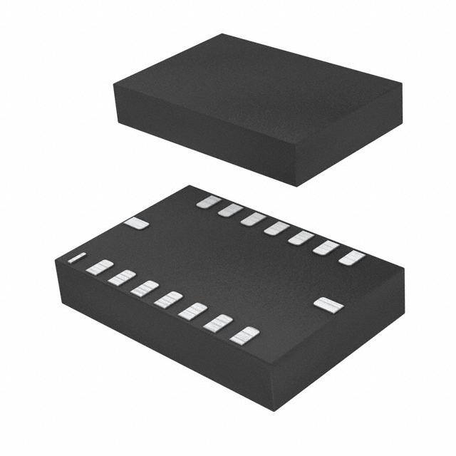
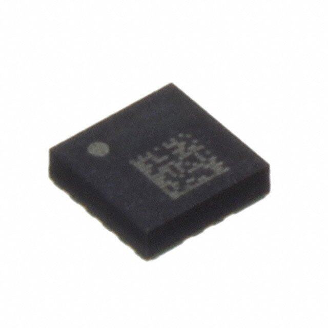
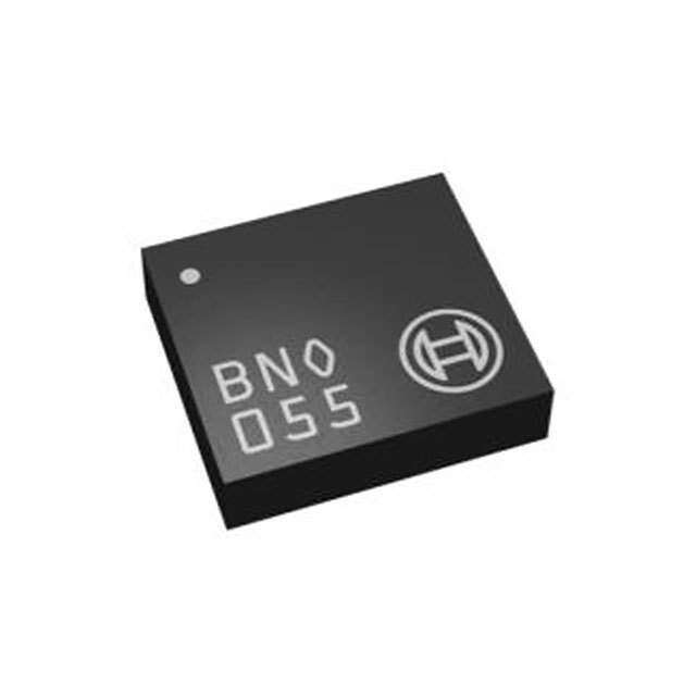
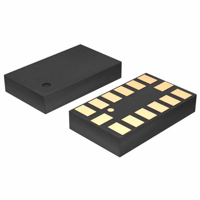
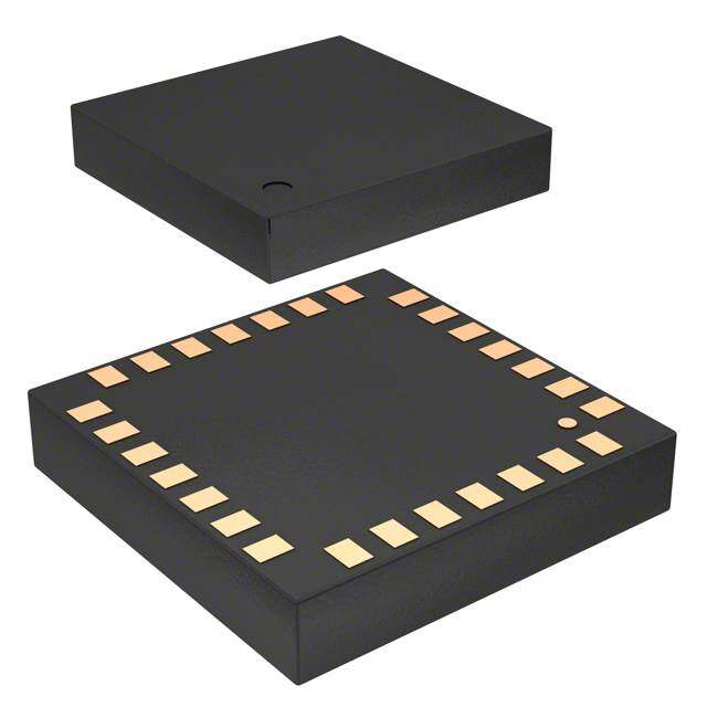
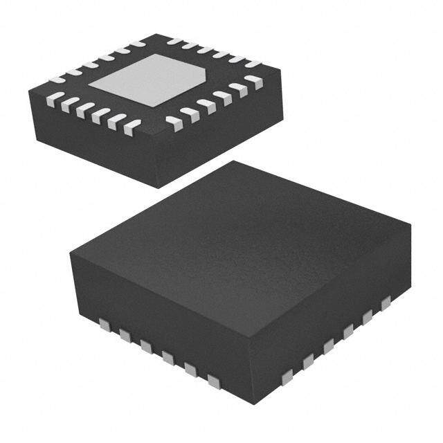
| 描述 | 6-AXIS ACCELEROMETER DIGITAL I/FIMU-惯性测量单元 6-Axis Inertia 3x4.5mm LGA-16 |
| 产品分类 | 加速计运动与定位传感器 |
| 品牌 | Bosch Sensortec |
| 产品手册 | |
| 产品图片 |
|
| rohs | 符合RoHS无铅 / 符合限制有害物质指令(RoHS)规范要求 |
| 产品系列 | IMU-惯性测量单元,Bosch Sensortec BMI055- |
| 数据手册 | |
| 产品型号 | BMI055 |
| 产品种类 | IMU-惯性测量单元 |
| 传感轴 | X, Y, Z |
| 供应商器件封装 | 16-QFN(3x4) |
| 其它名称 | 828-1043-1 |
| 加速 | 2 g, 4 g, 8 g, 16 g |
| 加速度范围 | ±2g, 4g, 8g, 16g |
| 商标 | Bosch Sensortec |
| 安装类型 | 表面贴装 |
| 封装 | Reel |
| 封装/外壳 | 16-VFQFN |
| 封装/箱体 | LGA-16 |
| 工厂包装数量 | 5000 |
| 带宽 | 8Hz ~ 1kHz |
| 接口 | I²C, SPI |
| 数字输出-位数 | 16 bit |
| 数字输出-总线接口 | I2C, SPI |
| 最大工作温度 | + 85 C |
| 最小工作温度 | - 40 C |
| 标准包装 | 1 |
| 灵敏度 | 1024LSB/g,512LSB/g,256LSB/g,128LSB/g |
| 电压-电源 | 2.4 V ~ 3.6 V |
| 电源电压-最大 | 3.6 V |
| 电源电压-最小 | 1.2 V |
| 电源电流 | 130 uA |
| 轴 | X,Y,Z |
| 输出类型 | I²C, SPI |
| 零件号别名 | 0273.141.134-1NV 828-1043-1-ND 828-1043-2-ND 828-1043-6-ND |


- 商务部:美国ITC正式对集成电路等产品启动337调查
- 曝三星4nm工艺存在良率问题 高通将骁龙8 Gen1或转产台积电
- 太阳诱电将投资9.5亿元在常州建新厂生产MLCC 预计2023年完工
- 英特尔发布欧洲新工厂建设计划 深化IDM 2.0 战略
- 台积电先进制程称霸业界 有大客户加持明年业绩稳了
- 达到5530亿美元!SIA预计今年全球半导体销售额将创下新高
- 英特尔拟将自动驾驶子公司Mobileye上市 估值或超500亿美元
- 三星加码芯片和SET,合并消费电子和移动部门,撤换高东真等 CEO
- 三星电子宣布重大人事变动 还合并消费电子和移动部门
- 海关总署:前11个月进口集成电路产品价值2.52万亿元 增长14.8%

PDF Datasheet 数据手册内容提取
Data sheet BMI055 Small, versatile 6DoF sensor module Bosch Sensortec BMI055: Data sheet Document revision 1.2 Document release date July 24th, 2014 Document number BST-BMI055-DS000-08 Technical reference code(s) 0 273 141 134 Notes Data and descriptions within this document are subject to change without notice. Product photos and pictures are for illustration purposes only and may differ from the real product’s appearance.
BMI055 Page 2 Data sheet BMI055 Basic Description Key features 2 inertial sensors in one device an advanced triaxial 16bit gyroscope and a versatile, leading edge triaxial 12bit accelerometer for reduced PCB space and simplified signal routing Small package LGA package 16 pins footprint 3.0 x 4.5 mm², height 0.95mm Common voltage supplies V voltage range: 2.4V to 3.6V DD Digital interface SPI (4-wire, 3-wire), I²C, 4 interrupt pins V voltage range: 1.2V to 3.6V DDIO Smart operation and integration Gyroscope and accelerometer can be operated individually Consumer electronics suite MSL1, RoHS compliant, halogen-free Operating temperature: -40°C ... +85°C 9DoF software compatible Accelerometer features Programmable functionality Acceleration ranges ±2g/±4g/±8g/±16g Low-pass filter bandwidths 1kHz - <8Hz On-chip FIFO Integrated FIFO with a depth of 32 frames On-chip interrupt controller Motion-triggered interrupt-signal generation for - new data - any-motion (slope) detection - tap sensing (single tap / double tap) - orientation- & motion inactivity recognition - flat/low-g/high-g detection On-chip temperature sensor factory trimmed, 8-bit, typical slope 0.5K/LSB. Ultra-low power IC 130µA current consumption, 1.3ms wake-up time, advanced features for system power management Gyroscope features Programmable functionality Ranges switchable from ±125°/s to ±2000°/s Low-pass filter bandwidths 230Hz - 12Hz Fast and slow offset controller (FOC and SOC) On-chip FIFO Integrated FIFO with a depth of 100 frames On-chip interrupt controller Motion-triggered interrupt-signal generation for - new data - any-motion (slope) detection - high rate Low power IC < 5mA current consumption, 30ms start-up time wake-up time in fast power-up mode only 10ms BST-BMI055-DS000-08 | Revision 1.2 | July 2014 Bosch Sensortec ©Bosch Sensortec GmbH reserves all rights even in the event of industrial property rights. We reserve all rights of disposal such as copying and passing on to third parties. BOSCH and the symbol are registered trademarks of Robert Bosch GmbH, Germany. Note: Specifications within this document are preliminary and subject to change without notice.
BMI055 Page 3 Data sheet Typical applications Advanced gaming & HMI Advanced gesture recognition Indoor navigation Image stabilization Display profile switching Advanced system power management for mobile applications Menu scrolling, tap / double tap sensing Pedometer / step counting Free-fall detection E-compass tilt compensation Drop detection for warranty logging General description The BMI055 is an inertial measurement unit (IMU) for the detection of movements and rotations in 6 degrees of freedom (6DoF). It reflects the full functionality of a triaxial, low-g acceleration sensor and at the same time it is capable to measure angular rates. Both – acceleration and angular rate – in three perpendicular room dimensions, the x-, y- and z-axis. The BMI055 is designed to meet all requirements for consumer applications such as gaming and pointing devices, HMI and image stabilization (DSC and camera-phone). It also senses tilt, motion, inactivity and shock vibration in cell phones, handhelds, computer peripherals, man- machine interfaces, virtual reality features and game controllers. An evaluation circuitry (ASIC) converts the output of the micro-electromechanical sensing structures (MEMS), developed, produced and tested in BOSCH facilities. The corresponding chip-sets are packed into one single LGA 3.0mm x 4.5mm x 0.95mm housing. For optimum system integration the BMI055 is fitted with digital bi-directional SPI and I2C interfaces. To provide maximum performance and reliability each device is tested and ready-to-use calibrated. Package and interfaces of the BMI055 have been defined to match a multitude of hardware requirements. Since the sensor features a small footprint, a flat package and very low power consumption it is ingeniously suited for mobile-phone and tablet PC applications. The BMI055 offers a variable V voltage range from 1.2V to 3.6V and can be programmed to DDIO optimize functionality, performance and power consumption in customer specific applications. In addition it features on-chip interrupt controllers enabling motion-based applications without use of a microcontroller. BST-BMI055-DS000-08 | Revision 1.2 | July 2014 Bosch Sensortec ©Bosch Sensortec GmbH reserves all rights even in the event of industrial property rights. We reserve all rights of disposal such as copying and passing on to third parties. BOSCH and the symbol are registered trademarks of Robert Bosch GmbH, Germany. Note: Specifications within this document are preliminary and subject to change without notice.
BMI055 Page 4 Data sheet Index of Contents BASIC DESCRIPTION ................................................................................................................... 2 1. SPECIFICATION ...................................................................................................................... 11 1.1 ELECTRICAL SPECIFICATION ............................................................................................... 11 1.2 ELECTRICAL AND PHYSICAL CHARACTERISTICS, MEASUREMENT PERFORMANCE .................... 12 2. ABSOLUTE MAXIMUM RATINGS .......................................................................................... 17 3. BLOCK DIAGRAM ................................................................................................................... 18 4. BASIC POWER MANAGEMENT ............................................................................................. 19 5. FUNCTIONAL DESCRIPTION ACCELEROMETER .............................................................. 20 5.1 POWER MODES ACCELEROMETER ...................................................................................... 20 5.2 IMU DATA ACCELEROMETER .............................................................................................. 24 5.2.1 ACCELERATION DATA ....................................................................................................................24 5.2.2 TEMPERATURE SENSOR ................................................................................................................25 5.3 SELF-TEST ACCELEROMETER ............................................................................................. 25 5.4 OFFSET COMPENSATION ACCELEROMETER ......................................................................... 26 5.4.1 SLOW COMPENSATION ..................................................................................................................28 5.4.2 FAST COMPENSATION ....................................................................................................................28 5.4.3 MANUAL COMPENSATION .............................................................................................................. 29 5.4.4 INLINE CALIBRATION ..................................................................................................................... 29 5.5 NON-VOLATILE MEMORY ACCELEROMETER ......................................................................... 30 5.6 INTERRUPT CONTROLLER ACCELEROMETER ....................................................................... 30 5.6.1 GENERAL FEATURES .....................................................................................................................31 5.6.2 MAPPING TO PHYSICAL INTERRUPT PINS (INTTYPE TO INT PIN#) .....................................................32 5.6.3 ELECTRICAL BEHAVIOR (INT PIN# TO OPEN-DRIVE OR PUSH-PULL) ..................................................32 5.6.4 NEW DATA INTERRUPT...................................................................................................................33 5.6.5 SLOPE / ANY-MOTION DETECTION ..................................................................................................33 5.6.6 ORIENTATION RECOGNITION ..........................................................................................................37 5.6.7 FLAT DETECTION ...........................................................................................................................41 5.6.8 LOW-G INTERRUPT ........................................................................................................................42 5.6.9 HIGH-G INTERRUPT .......................................................................................................................42 5.6.10 NO-MOTION / SLOW MOTION DETECTION .......................................................................................43 5.7 SOFTRESET ACCELEROMETER ........................................................................................... 44 6. REGISTER DESCRIPTION ACCELEROMETER ................................................................... 45 6.1 GENERAL REMARKS ACCELEROMETER ............................................................................... 45 6.2 REGISTER MAP ACCELEROMETER ...................................................................................... 46 ACC REGISTER 0X00 (BGW_CHIPID) ................................................................................... 47 BST-BMI055-DS000-08 | Revision 1.2 | July 2014 Bosch Sensortec ©Bosch Sensortec GmbH reserves all rights even in the event of industrial property rights. We reserve all rights of disposal such as copying and passing on to third parties. BOSCH and the symbol are registered trademarks of Robert Bosch GmbH, Germany. Note: Specifications within this document are preliminary and subject to change without notice.
BMI055 Page 5 Data sheet ACC REGISTER 0X01 IS RESERVED ......................................................................................... 47 ACC REGISTER 0X02 (ACCD_X_LSB) ................................................................................... 47 ACC REGISTER 0X03 (ACCD_X_MSB) .................................................................................. 48 ACC REGISTER 0X04 (ACCD_Y_LSB) ................................................................................... 48 ACC REGISTER 0X05 (ACCD_Y_MSB) .................................................................................. 49 ACC REGISTER 0X06 (ACCD_Z_LSB) ................................................................................... 49 ACC REGISTER 0X07 (ACCD_Z_MSB) .................................................................................. 50 ACC REGISTER 0X08 (ACCD_TEMP) .................................................................................... 50 ACC REGISTER 0X09 (INT_STATUS_0) ................................................................................ 51 ACC REGISTER 0X0A (INT_STATUS_1) ................................................................................ 52 ACC REGISTER 0X0B (INT_STATUS_2) ................................................................................ 52 ACC REGISTER 0X0C (INT_STATUS_3) ................................................................................ 53 ACC REGISTER 0X0D IS RESERVED ........................................................................................ 54 ACC REGISTER 0X0E (FIFO_STATUS) .................................................................................. 54 ACC REGISTER 0X0F (PMU_RANGE) ................................................................................... 54 ACC REGISTER 0X10 (PMU_BW) .......................................................................................... 55 ACC REGISTER 0X11 (PMU_LPW) ........................................................................................ 55 ACC REGISTER 0X12 (PMU_LOW_POWER)......................................................................... 56 ACC REGISTER 0X13 (ACCD_HBW) ...................................................................................... 57 ACC REGISTER 0X14 (BGW_SOFTRESET) .......................................................................... 57 ACC REGISTER 0X15 IS RESERVED ......................................................................................... 58 ACC REGISTER 0X16 (INT_EN_0) ......................................................................................... 58 ACC REGISTER 0X17 (INT_EN_1) ......................................................................................... 58 ACC REGISTER 0X18 (INT_EN_2) ......................................................................................... 59 ACC REGISTER 0X19 (INT_MAP_0) ....................................................................................... 59 ACC REGISTER 0X1A (INT_MAP_1) ...................................................................................... 60 ACC REGISTER 0X1B (INT_MAP_2) ...................................................................................... 61 ACC REGISTER 0X1C IS RESERVED ........................................................................................ 61 ACC REGISTER 0X1D IS RESERVED ........................................................................................ 61 ACC REGISTER 0X1E (INT_SRC) .......................................................................................... 61 ACC REGISTER 0X1F IS RESERVED ......................................................................................... 62 ACC REGISTER 0X20 (INT_OUT_CTRL) ................................................................................ 62 ACC REGISTER 0X21 (INT_RST_LATCH) .............................................................................. 62 ACC REGISTER 0X22 (INT_0) ................................................................................................ 63 ACC REGISTER 0X23 (INT_1) ................................................................................................ 63 BST-BMI055-DS000-08 | Revision 1.2 | July 2014 Bosch Sensortec ©Bosch Sensortec GmbH reserves all rights even in the event of industrial property rights. We reserve all rights of disposal such as copying and passing on to third parties. BOSCH and the symbol are registered trademarks of Robert Bosch GmbH, Germany. Note: Specifications within this document are preliminary and subject to change without notice.
BMI055 Page 6 Data sheet ACC REGISTER 0X24 (INT_2) ................................................................................................ 64 ACC REGISTER 0X25 (INT_3) ................................................................................................ 64 ACC REGISTER 0X26 (INT_4) ................................................................................................ 65 ACC REGISTER 0X27 (INT_5) ................................................................................................ 65 ACC REGISTER 0X28 (INT_6) ................................................................................................ 66 ACC REGISTER 0X29 (INT_7) ................................................................................................ 67 ACC REGISTER 0X2A (INT_8) ................................................................................................ 67 ACC REGISTER 0X2B (INT_9) ................................................................................................ 68 ACC REGISTER 0X2C (INT_A) ............................................................................................... 68 ACC REGISTER 0X2D (INT_B) ............................................................................................... 69 ACC REGISTER 0X2E (INT_C) ............................................................................................... 69 ACC REGISTER 0X2F (INT_D) ............................................................................................... 70 ACC REGISTER 0X30 (FIFO_CONFIG_0) .............................................................................. 70 ACC REGISTER 0X31 IS RESERVED ......................................................................................... 71 ACC REGISTER 0X32 (PMU_SELF_TEST) ............................................................................ 71 ACC REGISTER 0X33 (TRIM_NVM_CTRL) ............................................................................ 72 ACC REGISTER 0X34 (BGW_SPI3_WDT) .............................................................................. 72 ACC REGISTER 0X35 IS RESERVED ......................................................................................... 73 ACC REGISTER 0X36 (OFC_CTRL) ....................................................................................... 73 ACC REGISTER 0X37 (OFC_SETTING) ................................................................................. 74 ACC REGISTER 0X38 (OFC_OFFSET_X) .............................................................................. 74 ACC REGISTER 0X39 (OFC_OFFSET_Y) .............................................................................. 75 ACC REGISTER 0X3A (OFC_OFFSET_Z) .............................................................................. 76 ACC REGISTER 0X3B (TRIM_GP0) ........................................................................................ 76 ACC REGISTER 0X3C (TRIM_GP1) ........................................................................................ 77 ACC REGISTER 0X3D IS RESERVED ........................................................................................ 77 ACC REGISTER 0X3E (FIFO_CONFIG_1) .............................................................................. 77 ACC REGISTER 0X3F (FIFO_DATA) ...................................................................................... 78 7. FUNCTIONAL DESCRIPTION GYRO ..................................................................................... 79 7.1 POWER MODES GYROSCOPE ............................................................................................. 79 7.1.1 ADVANCED POWER-SAVING MODES ............................................................................................... 80 7.2 IMU DATA GYRO .............................................................................................................. 82 7.2.1 RATE DATA ...................................................................................................................................82 7.3 ANGULAR RATE READ-OUT ............................................................................................... 83 BST-BMI055-DS000-08 | Revision 1.2 | July 2014 Bosch Sensortec ©Bosch Sensortec GmbH reserves all rights even in the event of industrial property rights. We reserve all rights of disposal such as copying and passing on to third parties. BOSCH and the symbol are registered trademarks of Robert Bosch GmbH, Germany. Note: Specifications within this document are preliminary and subject to change without notice.
BMI055 Page 7 Data sheet 7.4 SELF-TEST GYRO .............................................................................................................. 83 7.5 OFFSET COMPENSATION GYROSCOPE ................................................................................ 84 7.5.1 SLOW COMPENSATION ..................................................................................................................84 7.5.2 FAST COMPENSATION ....................................................................................................................84 7.5.3 MANUAL COMPENSATION ...............................................................................................................85 7.5.4 INLINE CALIBRATION ......................................................................................................................85 7.6 NON-VOLATILE MEMORY GYROSCOPE ................................................................................. 85 7.7 INTERRUPT CONTROLLER GYRO ........................................................................................ 86 7.7.1 GENERAL FEATURES .................................................................................................................... 86 7.7.2 MAPPING TO PHYSICAL INTERRUPT PINS (INTTYPE TO INT PIN#)......................................................88 7.7.3 ELECTRICAL BEHAVIOR (INT PIN# TO OPEN-DRIVE OR PUSH-PULL) ..................................................88 7.7.4 NEW DATA INTERRUPT ...................................................................................................................88 7.7.5 ANY-MOTION DETECTION / INTERRUPT ...........................................................................................88 7.7.6 HIGH-RATE INTERRUPT ................................................................................................................ 90 8. REGISTER DESCRIPTION GYROSCOPE ............................................................................. 92 8.1 GENERAL REMARKS .......................................................................................................... 92 8.2 REGISTER MAP GYROSCOPE .............................................................................................. 93 GYR REGISTER 0X00 (CHIP_ID) ............................................................................................ 94 GYR REGISTER 0X01 IS RESERVED ......................................................................................... 94 GYR REGISTER 0X02 (RATE_X_LSB) ................................................................................... 94 GYR REGISTER 0X03 (RATE_X_MSB) .................................................................................. 95 GYR REGISTER 0X04 (RATE_Y_LSB) ................................................................................... 95 GYR REGISTER 0X05 (RATE_Y_MSB) .................................................................................. 96 GYR REGISTER 0X06 (RATE_Z_LSB) .................................................................................... 96 GYR REGISTER 0X07 (RATE_Z_MSB) ................................................................................... 97 GYR REGISTER 0X08 RESERVED ............................................................................................ 97 GYR REGISTER 0X09 (INT_STATUS_0) ................................................................................ 97 GYR REGISTER 0X0A (INT_STATUS_1) ................................................................................ 98 GYR REGISTER 0X0B (INT_STATUS_2) ................................................................................ 98 GYR REGISTER 0X0C (INT_STATUS_3) ................................................................................ 99 GYR REGISTER 0X0D IS RESERVED ........................................................................................ 99 GYR REGISTER 0X0E (FIFO_STATUS) .................................................................................. 99 GYR REGISTER 0X0F (RANGE) ........................................................................................... 100 GYR REGISTER 0X10 (BW) .................................................................................................. 100 GYR REGISTER 0X11 (LPM1) ............................................................................................... 101 GYR REGISTER 0X12 (LPM2)............................................................................................... 102 GYR REGISTER 0X13 (RATE_HBW) .................................................................................... 103 GYR REGISTER 0X14 (BGW_SOFTRESET) ........................................................................ 104 BST-BMI055-DS000-08 | Revision 1.2 | July 2014 Bosch Sensortec ©Bosch Sensortec GmbH reserves all rights even in the event of industrial property rights. We reserve all rights of disposal such as copying and passing on to third parties. BOSCH and the symbol are registered trademarks of Robert Bosch GmbH, Germany. Note: Specifications within this document are preliminary and subject to change without notice.
BMI055 Page 8 Data sheet GYR REGISTER 0X15 (INT_EN_0) ....................................................................................... 104 GYR REGISTER 0X16 (INT_EN_1) ....................................................................................... 105 GYR REGISTER 0X17 (INT_MAP_0) ..................................................................................... 105 GYR REGISTER 0X18 (INT_MAP_1) ..................................................................................... 106 GYR REGISTER 0X19 (INT_MAP_2)..................................................................................... 106 GYR REGISTER 0X1A ........................................................................................................... 107 GYR REGISTER 0X1B ........................................................................................................... 107 GYR REGISTER 0X1C .......................................................................................................... 108 GYR REGISTER 0X1D IS RESERVED. ..................................................................................... 108 GYR REGISTER 0X1E ........................................................................................................... 108 GYR REGISTER 0X1F AND 0X20 ARE RESERVED .................................................................... 109 GYR REGISTER 0X21 (INT_RST_LATCH) ............................................................................ 109 GYR REGISTER 0X22 (HIGH_TH_X) ...................................................................................... 109 GYR REGISTER 0X23 (HIGH_DUR_X) ................................................................................... 110 GYR REGISTER 0X24 (HIGH_TH_Y) ..................................................................................... 110 GYR REGISTER 0X25 (HIGH_DUR_Y) ................................................................................... 111 GYR REGISTER 0X26 (HIGH_TH_Z) ..................................................................................... 111 GYR REGISTER 0X27 (HIGH_DUR_Z) ................................................................................... 112 GYR REGISTER 0X28 TO 0X30 ARE RESERVED ...................................................................... 112 GYR REGISTER 0X31 (SOC) ................................................................................................ 112 GYR REGISTER 0X32 (A_FOC) ............................................................................................ 113 GYR REGISTER 0X33 (TRIM_NVM_CTRL) .......................................................................... 114 GYR REGISTER 0X34 (BGW_SPI3_WDT) ............................................................................ 114 GYR REGISTER 0X35 IS RESERVED ....................................................................................... 115 GYR REGISTER 0X36 (OFC1) .............................................................................................. 115 GYR REGISTER 0X37 (OFC2) .............................................................................................. 115 GYR REGISTER 0X38 (OFC3) .............................................................................................. 116 GYR REGISTER 0X39 (OFC4) .............................................................................................. 117 GYR REGISTER 0X3A (TRIM_GP0) ...................................................................................... 117 GYR REGISTER 0X3B (TRIM_GP1) ...................................................................................... 118 GYR REGISTER 0X3C (BIST) ............................................................................................... 118 GYR REGISTER 0X3D (FIFO_CONFIG_0) ............................................................................ 119 GYR REGISTER 0X3E (FIFO_CONFIG_1) ............................................................................ 119 9. DIGITAL INTERFACE OF THE DEVICE ............................................................................... 121 BST-BMI055-DS000-08 | Revision 1.2 | July 2014 Bosch Sensortec ©Bosch Sensortec GmbH reserves all rights even in the event of industrial property rights. We reserve all rights of disposal such as copying and passing on to third parties. BOSCH and the symbol are registered trademarks of Robert Bosch GmbH, Germany. Note: Specifications within this document are preliminary and subject to change without notice.
BMI055 Page 9 Data sheet 9.1 SERIAL PERIPHERAL INTERFACE (SPI) .............................................................................. 122 9.2 INTER-INTEGRATED CIRCUIT (I²C) .................................................................................... 126 9.2.1 SPI AND I²C ACCESS RESTRICTIONS .......................................................................................... 129 10. FIFO OPERATION ............................................................................................................... 130 10.1 FIFO OPERATING MODES ............................................................................................. 130 10.2 FIFO DATA READOUT ................................................................................................... 131 10.2.1 DATA READOUT ACCELEROMETER .............................................................................................131 10.2.2 DATA READOUT GYROSCOPE ....................................................................................................132 10.2.3 EXTERNAL FIFO SYNCHRONIZATION (EFS) FOR THE GYROSCOPE ..............................................132 10.2.4 INTERFACE SPEED REQUIREMENTS FOR GYROSCOPE FIFO USE .................................................133 10.3 FIFO FRAME COUNTER AND OVERRUN FLAG ................................................................. 133 10.4 FIFO INTERRUPTS ........................................................................................................ 134 11. PIN-OUT AND CONNECTION DIAGRAM .......................................................................... 135 11.1 PIN-OUT ....................................................................................................................... 135 11.2 CONNECTION DIAGRAM 4 WIRE SPI ................................................................................ 136 11.3 CONNECTION DIAGRAM 3-WIRE SPI ............................................................................... 137 11.4 CONNECTION DIAGRAM I2C ............................................................................................ 138 12. PACKAGE ............................................................................................................................ 139 12.1 OUTLINE DIMENSIONS ................................................................................................... 139 12.2 SENSING AXES ORIENTATION ......................................................................................... 140 12.3 LANDING PATTERN RECOMMENDATION ........................................................................... 142 12.4 MARKING ..................................................................................................................... 143 12.4.1 MASS PRODUCTION SAMPLES ....................................................................................................143 12.4.2 ENGINEERING SAMPLES ............................................................................................................143 12.5 SOLDERING GUIDELINES ................................................................................................ 144 12.6 HANDLING INSTRUCTIONS .............................................................................................. 145 12.7 TAPE AND REEL SPECIFICATION...................................................................................... 145 12.7.1 ORIENTATION WITHIN THE REEL ................................................................................................ 146 12.8 ENVIRONMENTAL SAFETY .............................................................................................. 146 12.8.1 HALOGEN CONTENT ................................................................................................................. 146 12.8.2 INTERNAL PACKAGE STRUCTURE............................................................................................... 146 13. LEGAL DISCLAIMER .......................................................................................................... 147 13.1 ENGINEERING SAMPLES................................................................................................. 147 13.2 PRODUCT USE .............................................................................................................. 147 13.3 APPLICATION EXAMPLES AND HINTS ............................................................................... 147 BST-BMI055-DS000-08 | Revision 1.2 | July 2014 Bosch Sensortec ©Bosch Sensortec GmbH reserves all rights even in the event of industrial property rights. We reserve all rights of disposal such as copying and passing on to third parties. BOSCH and the symbol are registered trademarks of Robert Bosch GmbH, Germany. Note: Specifications within this document are preliminary and subject to change without notice.
BMI055 Page 10 Data sheet 14. DOCUMENT HISTORY AND MODIFICATION ................................................................... 148 BST-BMI055-DS000-08 | Revision 1.2 | July 2014 Bosch Sensortec ©Bosch Sensortec GmbH reserves all rights even in the event of industrial property rights. We reserve all rights of disposal such as copying and passing on to third parties. BOSCH and the symbol are registered trademarks of Robert Bosch GmbH, Germany. Note: Specifications within this document are preliminary and subject to change without notice.
BMI055 Page 11 Data sheet 1. Specification If not stated otherwise, the given values are over lifetime and full performance temperature and voltage ranges, minimum/maximum values are ±3. 1.1 Electrical specification Table 1: Electrical parameter specification OPERATING CONDITIONS Parameter Symbol Condition Min Typ Max Unit Supply Voltage V 2.4 3.0 3.6 V Internal Domains DD Supply Voltage V 1.2 2.4 3.6 V I/O Domain DDIO Voltage Input V SPI & I²C 0.3V - Low Level IL,a DDIO Voltage Input V SPI & I²C 0.7V - High Level IH,a DDIO Voltage Output V I = 3mA, SPI & I²C 0.23V Low Level OL,a OL DDIO - Voltage Output V I = 3mA, SPI 0.8V - High Level OH OH DDIO Operating T -40 +85 °C Temperature A BST-BMI055-DS000-08 | Revision 1.2 | July 2014 Bosch Sensortec ©Bosch Sensortec GmbH reserves all rights even in the event of industrial property rights. We reserve all rights of disposal such as copying and passing on to third parties. BOSCH and the symbol are registered trademarks of Robert Bosch GmbH, Germany. Note: Specifications within this document are preliminary and subject to change without notice.
BMI055 Page 12 Data sheet 1.2 Electrical and physical characteristics, measurement performance Table 2: Electrical characteristics accelerometer OPERATING CONDITIONS ACCELEROMETER Parameter Symbol Condition Min Typ Max Units g ±2 g FS2g Selectable g ±4 g FS4g Acceleration Range via serial digital g ±8 g FS8g interface g ±16 g FS16g Total Supply Current in I see1 130 µA DD Normal Mode Total Supply Current in I 2.1 µA DDsum see1 Suspend Mode Total Supply Current in I see1 1.0 µA Deep Suspend DDdsum Mode Total Supply I see1 Current in DDlp1 6.5 µA sleep duration ≥ 25ms Low-power Mode 1 Total Supply I see1 Current in DDlp2 66 µA sleep duration ≥ 25ms Low-power Mode 2 Total Supply Current in I see1 62 µA DDsbm Standby Mode from Low-power Mode 1 or Suspend Mode or Wake-Up Time 1 t 1.3 ms w,up1 Deep Suspend Mode bw = 1kHz from Low-power Mode Wake-Up Time 2 t 2 or Stand-by Mode 1 ms w,up2 bw = 1kHz Start-Up Time t POR, bw = 1kHz 3 ms s,up Non-volatile memory (NVM) n 15 Cycles NVM write-cycles 1 Conditions of current consumption if not specified otherwise: T =25°C, BW_Accel=1kHz, V = A DD V = 2.4V, digital protocol on, no streaming data DDIO BST-BMI055-DS000-08 | Revision 1.2 | July 2014 Bosch Sensortec ©Bosch Sensortec GmbH reserves all rights even in the event of industrial property rights. We reserve all rights of disposal such as copying and passing on to third parties. BOSCH and the symbol are registered trademarks of Robert Bosch GmbH, Germany. Note: Specifications within this document are preliminary and subject to change without notice.
BMI055 Page 13 Data sheet OUTPUT SIGNAL ACCELEROMETER Parameter Symbol Condition Min Typ Max Units Sensitivity S g , T =25°C 1024 LSB/g 2g FS2g A S g , T =25°C 512 LSB/g 4g FS4g A S g , T =25°C 256 LSB/g 8g FS8g A S g , T =25°C 128 LSB/g 16g FS16g A Sensitivity TCS g , ±0.02 %/K FS2g Temperature Drift Nominal V supplies DD Sensitivity S g , T =25°C, 0.05 %/V VDD FS2g A Supply Volt. Drift V ≤ V ≤ V DD_min DD DD_max Zero-g Offset (x,z) Off g , T =25°C, nominal ±70 mg x,z FS2g A V supplies, over life- DD time Zero-g Offset (y) Off g , T =25°C, nominal ±70 mg y FS2g A V supplies, over life- DD time Zero-g Offset TCO g , ±1 mg/K FS2g Temperature Drift Nominal V supplies DD Zero-g Offset Off g , T =25°C, 0.5 mg/V VDD FS2g A Supply Volt. Drift V ≤ V ≤ V DD_min DD DD_max Bandwidth bw 2nd order filter, 8 Hz 8 bandwidth bw 16 Hz 16 programmable bw 31 Hz 31 bw 63 Hz 63 bw 125 Hz 125 bw 250 Hz 250 bw 500 Hz 500 bw 1,000 Hz 1000 Nonlinearity NL best fit straight line, ±0.5 %FS g FS2g Output Noise n g , T =25°C 150 µg/Hz rms FS2g A Density Nominal V supplies DD Normal mode Temperature Sensor T -40 85 °C S Measurement Range Temperature Sensor dT 0.5 K/LSB S Slope Temperature Sensor OT ±2 K S Offset BST-BMI055-DS000-08 | Revision 1.2 | July 2014 Bosch Sensortec ©Bosch Sensortec GmbH reserves all rights even in the event of industrial property rights. We reserve all rights of disposal such as copying and passing on to third parties. BOSCH and the symbol are registered trademarks of Robert Bosch GmbH, Germany. Note: Specifications within this document are preliminary and subject to change without notice.
BMI055 Page 14 Data sheet MECHANICAL CHARACTERISTICS ACCELEROMETER Parameter Symbol Condition Min Typ Max Units relative contribution Cross Axis S between any two of the 1 % Sensitivity three axes relative to package Alignment Error E ±0.5 ° A outline Table 3: Electrical characteristics gyroscope OPERATING CONDITIONS GYROSCOPE Parameter Symbol Condition Min Typ Max Unit R 125 °/s FS125 R 250 °/s FS250 Selectable Range R 500 °/s FS500 via serial digital interface R 1,000 °/s FS1000 R 2,000 °/s FS2000 Supply Current in I see2 5 mA Normal Mode DD Supply Current in Fast Power-up I see2 2.5 mA DDfpm Mode Supply Current in see2, digital and analog I 25 µA Suspend Mode DDsum (only IF active) Supply Current in Deep Suspend I see2 <5 µA DDdsum Mode to ±1º/s of final Start-up time t 30 ms su value;from power-off From suspend- and Wake-up time t 30 ms wusm deep suspend-modes From fast power-up Wake-up time t 10 ms wufpm mode Non-volatile memory (NVM) n 15 cycles NVM write-cycles 2 Conditions of current consumption if not specified otherwise: T =25°C, BW_Gyro=1kHz, A V =2.4V, V =1.8V, digital protocol on, no streaming data DD DDIO BST-BMI055-DS000-08 | Revision 1.2 | July 2014 Bosch Sensortec ©Bosch Sensortec GmbH reserves all rights even in the event of industrial property rights. We reserve all rights of disposal such as copying and passing on to third parties. BOSCH and the symbol are registered trademarks of Robert Bosch GmbH, Germany. Note: Specifications within this document are preliminary and subject to change without notice.
BMI055 Page 15 Data sheet OUTPUT SIGNAL GYROSCOPE Parameter Symbol Condition Min Typ Max Unit Sensitivity Ta=25°C, R 16.4 LSB/°/s FS2000 Ta=25°C, R 32.8 LSB/°/s FS1000 Ta=25°C, R 65.6 LSB/°/s FS500 Ta=25°C, R 131.2 LSB/°/s FS250 Ta=25°C, R 262.4 LSB/°/s FS125 Sensitivity tolerance Ta=25°C, R ±1 % FS2000 Sensitivity Change TCS Nominal V supplies ±0.03 %/K DD over Temperature -40°C ≤ T ≤ +85°C A R FS2000 Sensitivity SVDD TA=25°C, <0.4 %/V Supply Volt. Drift V ≤ V ≤ V DD_min DD DD_max Nonlinearity NL best fit straight line ±0.05 %FS R R FS1000, FS2000 g- Sensitivity Sensitivity to 0.1 °/s/g acceleration stimuli in all three axis (frequency <20kHz) Zero-rate Offset Off Nominal V supplies ±1 °/s x DD T =25°C, slow and fast y and z A offset cancellation off Zero- Offset TCO Nominal V supplies ±0.015 °/s per K DD Change over -40°C ≤ T ≤ +85°C A Temperature R FS2000 T =25°C, Zero- Offset Off A <0.1 °/s /V VDD V ≤ V ≤ V Supply Volt. Drift DD_min DD DD_max Output Noise n rms, BW=47Hz 0.1 °/s rms (@ 0.014°/s/√Hz) BST-BMI055-DS000-08 | Revision 1.2 | July 2014 Bosch Sensortec ©Bosch Sensortec GmbH reserves all rights even in the event of industrial property rights. We reserve all rights of disposal such as copying and passing on to third parties. BOSCH and the symbol are registered trademarks of Robert Bosch GmbH, Germany. Note: Specifications within this document are preliminary and subject to change without notice.
BMI055 Page 16 Data sheet unfiltered 230 116 64 Bandwidth BW f Hz -3dB 47 32 23 12 2000 1000 Data rate 400 Hz (set of x,y,z rate) 200 100 Data rate tolerance ±0.3 % (set of x,y,z rate) Cross Axis Sensitivity to stimuli in ±1 % Sensitivity non-sense-direction BST-BMI055-DS000-08 | Revision 1.2 | July 2014 Bosch Sensortec ©Bosch Sensortec GmbH reserves all rights even in the event of industrial property rights. We reserve all rights of disposal such as copying and passing on to third parties. BOSCH and the symbol are registered trademarks of Robert Bosch GmbH, Germany. Note: Specifications within this document are preliminary and subject to change without notice.
BMI055 Page 17 Data sheet 2. Absolute maximum ratings Table 4: Absolute maximum ratings Parameter Condition Min Max Units Voltage at Supply Pin V Pin -0.3 4.25 V DD V Pin -0.3 4.25 V DDIO Voltage at any Logic Pin Non-Supply Pin -0.3 V +0.3 V DDIO Passive Storage Temp. Range ≤ 65% rel. H. -50 +150 °C None-volatile memory (NVM) T = 85°C, 10 y Data Retention after 15 cycles Duration ≤ 200µs 10,000 g Duration ≤ 1.0ms 2,000 g Mechanical Shock Free fall 1.8 m onto hard surfaces HBM, at any Pin 2 kV ESD CDM 500 V MM 200 V Note: Stress above these limits may cause damage to the device. Exceeding the specified electrical limits may affect the device reliability or cause malfunction. BST-BMI055-DS000-08 | Revision 1.2 | July 2014 Bosch Sensortec ©Bosch Sensortec GmbH reserves all rights even in the event of industrial property rights. We reserve all rights of disposal such as copying and passing on to third parties. BOSCH and the symbol are registered trademarks of Robert Bosch GmbH, Germany. Note: Specifications within this document are preliminary and subject to change without notice.
BMI055 Page 18 Data sheet 3. Block diagram Figure 1 shows the basic building blocks of the BMI055: Figure 1: Block diagram of the BMI055 BST-BMI055-DS000-08 | Revision 1.2 | July 2014 Bosch Sensortec ©Bosch Sensortec GmbH reserves all rights even in the event of industrial property rights. We reserve all rights of disposal such as copying and passing on to third parties. BOSCH and the symbol are registered trademarks of Robert Bosch GmbH, Germany. Note: Specifications within this document are preliminary and subject to change without notice.
BMI055 Page 19 Data sheet 4. Basic power management The BMI055 has two distinct power supply pins: • V is the main power supply for the internal blocks DD • V is a separate power supply pin mainly used for the supply of the interface DDIO There are no limitations on the voltage levels of both pins relative to each other, as long as each of them lies within its operating range. Furthermore, the device can be completely switched off (V = 0V) while keeping the V supply on (V > 0V) or vice versa. DD DDIO DDIO When the V supply is switched off, all interface pins (CSB, SDI, SCK, PS) must be kept DDIO close to GND potential. IO The device contains a power-on reset (POR) generator. It resets the logic part and the register values after powering-on V and V . Please note, that all application specific settings which DD DDIO are not equal to the default settings (refer to 6.2 register map accelerometer and to 8.2 register map gyroscope), must be re-set to its designated values after POR. In case the I²C interface shall be used, a direct electrical connection between V supply and DDIO the PS pin is needed in order to ensure reliable protocol selection. For SPI interface mode the PS pin must be directly connected to GND . IO BST-BMI055-DS000-08 | Revision 1.2 | July 2014 Bosch Sensortec ©Bosch Sensortec GmbH reserves all rights even in the event of industrial property rights. We reserve all rights of disposal such as copying and passing on to third parties. BOSCH and the symbol are registered trademarks of Robert Bosch GmbH, Germany. Note: Specifications within this document are preliminary and subject to change without notice.
BMI055 Page 20 Data sheet 5. Functional description accelerometer Note: Default values for registers can be found in chapter 6. 5.1 Power modes accelerometer The accelerometer has six different power modes. Besides normal mode, which represents the fully operational state of the device, there are five energy saving modes: deep-suspend mode, suspend mode, standby mode, low-power mode 1 and low-power mode 2. The possible transitions between the power modes are illustrated in figure 2: DDEEEEPP-- SSUUSSPPEENNDD MMooddee NNOORRMMAALL SSTTAANNDDBBYY SSUUSSPPEENNDD MMooddee MMooddee MMooddee LLooww PPoowweerr LLooww PPoowweerr MMooddee 11 MMooddee 22 Figure 2: Power mode transition diagram After power-up accelerometer is in normal mode so that all parts of the device are held powered-up and data acquisition is performed continuously. In deep-suspend mode the device reaches the lowest possible power consumption. Only the interface section is kept alive. No data acquisition is performed and the content of the configuration registers is lost. Deep suspend mode is entered (left) by writing ‘1’ (‘0’) to the (ACC 0x11) deep_suspend bit while (ACC 0x11) suspend bit is set to ‘0’. The I2C watchdog timer remains functional. The (ACC 0x11) deep_ suspend bit, the (ACC 0x34) spi3 bit, (ACC 0x34) i2c_wdt_en bit and the (ACC 0x34) i2c_wdt_sel bit are functional in deep-suspend mode. Equally the interrupt level and driver configuration registers (ACC 0x20) int1_lvl, (ACC 0x20) BST-BMI055-DS000-08 | Revision 1.2 | July 2014 Bosch Sensortec ©Bosch Sensortec GmbH reserves all rights even in the event of industrial property rights. We reserve all rights of disposal such as copying and passing on to third parties. BOSCH and the symbol are registered trademarks of Robert Bosch GmbH, Germany. Note: Specifications within this document are preliminary and subject to change without notice.
BMI055 Page 21 Data sheet int1_od, (ACC 0x20) int2_lvl, and (ACC 0x20) int2_od are accessible. Still it is possible to enter normal mode by performing a softreset as described in chapter 5.7. Please note, that all application specific settings which are not equal to the default settings (refer to 6.2 register map accelerometer), must be re-set to its designated values after leaving deep-suspend mode. In suspend mode the whole analog part is powered down. No data acquisition is performed. While in suspend mode the latest acceleration data and the content of all configuration registers are kept. Writing to and reading from registers is supported except from the (0x3E) fifo_config_1, (0x30) fifo_config_0 and (0x3F) fifo_data register. It is possible to enter normal mode by performing a softreset as described in chapter 5.7. Suspend mode is entered (left) by writing ´1´ (´0´) to the (ACC 0x11) suspend bit after bit (ACC 0x12) lowpower_mode has been set to ‘0’. Although write access to registers is supported at the full interface clock speed (SCL or SCK), a waiting period must be inserted between two consecutive write cycles (please refer also to section 9.2.1). In standby mode the analog part is powered down, while the digital part remains largely operational. No data acquisition is performed. Reading and writing registers is supported without any restrictions. The latest acceleration data and the content of all configuration registers are kept. Standby mode is entered (left) by writing ´1´ (´0´) to the (ACC 0x11) suspend bit after bit (ACC 0x12) lowpower_mode has been set to ‘1’. It is also possible to enter normal mode by performing a softreset as described in chapter 5.7. In low-power mode 1, the device is periodically switching between a sleep phase and a wake- up phase. The wake-up phase essentially corresponds to operation in normal mode with complete power-up of the circuitry. The sleep phase essentially corresponds to operation in suspend mode. Low-power mode is entered (left) by writing ´1´ (´0´) to the (ACC 0x11) lowpower_en bit with bit (ACC 0x12) lowpower_mode set to ‘0’. Read access to registers is possible except from the (0x3F) fifo_data register. However, unless the register access is synchronised with the wake-up phase, the restrictions of the suspend mode apply. Low-power mode 2 is very similar to low-power mode 1, but register access is possible at any time without restrictions. It consumes more power than low-power mode 1. In low-power mode 2 the device is periodically switching between a sleep phase and a wake-up phase. The wake- up phase essentially corresponds to operation in normal mode with complete power-up of the circuitry. The sleep phase essentially corresponds to operation in standby mode. Low-power mode is entered (left) by writing ´1´ (´0´) to the (ACC 0x11) lowpower_en bit with bit (ACC 0x12) lowpower_mode set to ‘1’. The timing behaviour of the low-power modes 1 and 2 depends on the setting of the (ACC 0x12) sleeptimer_en bit. When (ACC 0x12) sleeptimer_en is set to ‘0’, the event-driven time- base mode (EDT) is selected. In EDT the duration of the wake-up phase depends on the number of samples required by the enabled interrupt engines. If an interrupt is detected, the device stays in the wake-up phase as long as the interrupt condition endures (non-latched interrupt), or until the latch time expires (temporary interrupt), or until the interrupt is reset (latched interrupt). If no interrupt is detected, the device enters the sleep phase immediately after the required number of acceleration samples have been taken and an active interface access cycle has ended. The EDT mode is recommended for power-critical applications which do not use the FIFO. Also, EDT mode is compatible with legacy BST sensors. Figure 3 shows the timing diagram for low-power modes 1 and 2 when EDT is selected. BST-BMI055-DS000-08 | Revision 1.2 | July 2014 Bosch Sensortec ©Bosch Sensortec GmbH reserves all rights even in the event of industrial property rights. We reserve all rights of disposal such as copying and passing on to third parties. BOSCH and the symbol are registered trademarks of Robert Bosch GmbH, Germany. Note: Specifications within this document are preliminary and subject to change without notice.
BMI055 Page 22 Data sheet t State ACTIVE Active phase e e e e e e ettle mple ettle ampl ampl ampl ampl ampl ettleampl S a S S S S S S SS Sleep phase S t t SLEEP SLEEP t Figure 3: Timing Diagram for low-power mode 1/2, EDT When (ACC 0x12) sleeptimer_en is set to ‘1’, the equidistant-sampling mode (EST) is selected. The use of the EST mode is recommended when the FIFO is used since it ensures that equidistant samples are sampled into the FIFO regardless of whether the active phase is extended by active interrupt engines or interface activity. In EST mode the sleep time t is SLEEP defined as shown in figure 4. The FIFO sampling time t is the sum of the sleep time t SAMPLE SLEEP and the sensor data sampling time t . Since interrupt engines can extend the active phase to SSMP exceed the sleep time t , equidistant sampling is only guaranteed if the bandwidth has been SLEEP chosen such that 1/(2 * bw) = n * t where n is an integer. If this condition is infringed, SLEEP equidistant sampling is not possible. Once the sleep time has elapsed the device will store the next available sample in the FIFO. This set-up condition is not recommended as it may result in timing jitter. Sampled into FIFO State Active phase e e e e e e e ettle mple ettle ampl ampl ampl ampl ampl ettleampl ettleampl S a S S S S S S SS SS Sleep phase S t t t SLEEP SLEEP SLEEP t SSMP t t t SAMPLE SAMPLE SAMPLE t Figure 4: Timing Diagram for low-power mode 1/2, EST The sleep time for lower-power mode 1 and 2 is set by the (ACC 0x11) sleep_dur bits as shown BST-BMI055-DS000-08 | Revision 1.2 | July 2014 Bosch Sensortec ©Bosch Sensortec GmbH reserves all rights even in the event of industrial property rights. We reserve all rights of disposal such as copying and passing on to third parties. BOSCH and the symbol are registered trademarks of Robert Bosch GmbH, Germany. Note: Specifications within this document are preliminary and subject to change without notice.
BMI055 Page 23 Data sheet in the following table: Table 5: Sleep phase duration settings Sleep Phase (ACC 0x11) Duration sleep_dur t sleep 0000b 0.5ms 0001b 0.5ms 0010b 0.5ms 0011b 0.5ms 0100b 0.5ms 0101b 0.5ms 0110b 1ms 0111b 2ms 1000b 4ms 1001b 6ms 1010b 10ms 1011b 25ms 1100b 50ms 1101b 100ms 1110b 500ms 1111b 1s The current consumption of the accelerometer in low-power mode 1 (I ) and low-power DDlp1 mode 2 (I ) can be estimated according to the following formulae: DDlp2 t I t I I sleep DDsum active DD . DDlp1 t t sleep active t I t I I sleep DDsbm active DD DDlp2 t t sleep active When estimating the length of the wake-up phase t , the corresponding typical wake-up time, active t or t and t (given in table 6) have to be considered: w,up1 w,up2 ut If bandwidth is >=31.25 Hz: t = t + t – 0.9 ms (or t = t + t – 0.9 ms) active ut w,up1 active ut w,up2 else: t = 4 t + t – 0.9 ms (or t = 4 t + t – 0.9 ms) active ut w,up1 active ut w,up2 During the wake-up phase all analog modules are held powered-up, while during the sleep phase most analog modules are powered down. Consequently, a wake-up time of more than t (t ) ms is needed to settle the analog modules so that reliable acceleration data are w,up1 w,up2 generated. BST-BMI055-DS000-08 | Revision 1.2 | July 2014 Bosch Sensortec ©Bosch Sensortec GmbH reserves all rights even in the event of industrial property rights. We reserve all rights of disposal such as copying and passing on to third parties. BOSCH and the symbol are registered trademarks of Robert Bosch GmbH, Germany. Note: Specifications within this document are preliminary and subject to change without notice.
BMI055 Page 24 Data sheet 5.2 IMU data accelerometer 5.2.1 Acceleration data The width of acceleration data is 12 bits given in two´s complement representation. The 12 bits for each axis are split into an MSB upper part (one byte containing bits 11 to 4) and an LSB lower part (one byte containing bits 3 to 0 of acceleration and a (ACC 0x02, 0x04, 0x06) new_data flag). Reading the acceleration data registers shall always start with the LSB part. In order to ensure the integrity of the acceleration data, the content of an MSB register is locked by reading the corresponding LSB register (shadowing procedure). When shadowing is enabled, the MSB must always be read in order to remove the data lock. The shadowing procedure can be disabled (enabled) by writing ´1´ (´0´) to the bit shadow_dis. With shadowing disabled, the content of both MSB and LSB registers is updated by a new value immediately. Unused bits of the LSB registers may have any value and should be ignored. The (ACC 0x02, 0x04, 0x06) new_data flag of each LSB register is set if the data registers have been updated. The flag is reset if either the corresponding MSB or LSB part is read. Two different streams of acceleration data are available, unfiltered and filtered. The unfiltered data is sampled with 2kHz. The sampling rate of the filtered data depends on the selected filter bandwidth and is always twice the selected bandwidth (BW = ODR/2). Which kind of data is stored in the acceleration data registers depends on bit (ACC 0x13) data_high_bw. If (ACC 0x13) data_high_bw is ´0´ (´1´), then filtered (unfiltered) data is stored in the registers. Both data streams are offset-compensated. The bandwidth of filtered acceleration data is determined by setting the (ACC 0x10) bw bit as followed: Table 6: Bandwidth configuration Update Time bw Bandwidth t ut 00xxx *) - 01000 7.81Hz 64ms 01001 15.63Hz 32ms 01010 31.25Hz 16ms 01011 62.5Hz 8ms 01100 125Hz 4ms 01101 250Hz 2ms 01110 500Hz 1ms 01111 1000Hz 0.5ms 1xxxx *) - *) Note: Settings 00xxx result in a bandwidth of 7.81 Hz; settings 1xxxx result in a bandwidth of 1000 Hz. It is recommended to actively set an application specific and an appropriate bandwidth and to use the range from ´01000b´ to ´01111b´ only in order to be compatible with future products. BST-BMI055-DS000-08 | Revision 1.2 | July 2014 Bosch Sensortec ©Bosch Sensortec GmbH reserves all rights even in the event of industrial property rights. We reserve all rights of disposal such as copying and passing on to third parties. BOSCH and the symbol are registered trademarks of Robert Bosch GmbH, Germany. Note: Specifications within this document are preliminary and subject to change without notice.
BMI055 Page 25 Data sheet The accelerometer supports four different acceleration measurement ranges. A measurement range is selected by setting the (ACC 0x0F) range bits as follows: Table 7: Range selection Acceleration Range measurement Resolution range 0011 ±2g 0.98mg/LSB 0101 ±4g 1.95mg/LSB 1000 ±8g 3.91mg/LSB 1100 ±16g 7.81mg/LSB others reserved - 5.2.2 Temperature Sensor The width of temperature data is 8 bits given in two´s complement representation. Temperature values are available in the (ACC 0x08) temp register. The slope of the temperature sensor is 0.5K/LSB, its center temperature is 23°C [(ACC 0x08) temp = 0x00]. 5.3 Self-test accelerometer This feature permits to check the sensor functionality by applying electrostatic forces to the sensor core instead of external accelerations. By actually deflecting the seismic mass, the entire signal path of the sensor can be tested. Activating the self-test results in a static offset of the acceleration data; any external acceleration or gravitational force applied to the sensor during active self-test will be observed in the output as a superposition of both acceleration and self-test signal. Before the self-test is enabled the g-range should be set to 8 g. The self-test is activated individually for each axis by writing the proper value to the (ACC 0x32) self_test_axis bits (´01b´ for x-axis, ´10b´ for y-axis, ´11b´ for z-axis, ´00b´ to deactivate self-test). It is possible to control the direction of the deflection through bit (ACC 0x32) self_test_sign. The excitation occurs in negative (positive) direction if (ACC 0x32) self_test_sign = ´0b´ (´1b´). The amplitude of the deflection has to be set high by writing (ACC 0x32) self_test_amp=´1b´. After the self-test is enabled, the user should wait 50ms before interpreting the acceleration data. In order to ensure a proper interpretation of the self-test signal it is recommended to perform the self-test for both (positive and negative) directions and then to calculate the difference of the resulting acceleration values. Table 8 shows the minimum differences for each axis. The actually measured signal differences can be significantly larger. BST-BMI055-DS000-08 | Revision 1.2 | July 2014 Bosch Sensortec ©Bosch Sensortec GmbH reserves all rights even in the event of industrial property rights. We reserve all rights of disposal such as copying and passing on to third parties. BOSCH and the symbol are registered trademarks of Robert Bosch GmbH, Germany. Note: Specifications within this document are preliminary and subject to change without notice.
BMI055 Page 26 Data sheet Table 8: Self-test difference values x-axis signal y-axis signal z-axis signal resulting minimum 800 mg 800 mg 400 mg difference signal It is recommended to perform a reset of the device after a self-test has been performed. If the reset cannot be performed, the following sequence must be kept to prevent unwanted interrupt generation: disable interrupts, change parameters of interrupts, wait for at least 50ms, enable desired interrupts. 5.4 Offset compensation accelerometer Offsets in measured signals can have several causes but they are always unwanted and disturbing in many cases. Therefore, the accelerometer offers an advanced set of four digital offset compensation methods which are closely matched to each other. These are slow, fast, and manual compensation as well as inline calibration. The compensation is performed with filtered data, and is then applied to both, unfiltered and filtered data. If necessary the result of this computation is saturated to prevent any overflow errors (the smallest or biggest possible value is set, depending on the sign). However, the registers used to read and write compensation values have a width of 8 bits. BST-BMI055-DS000-08 | Revision 1.2 | July 2014 Bosch Sensortec ©Bosch Sensortec GmbH reserves all rights even in the event of industrial property rights. We reserve all rights of disposal such as copying and passing on to third parties. BOSCH and the symbol are registered trademarks of Robert Bosch GmbH, Germany. Note: Specifications within this document are preliminary and subject to change without notice.
BMI055 Page 27 Data sheet An overview of the offset compensation principle is given in figure 5: I2C/SPI/NVM mapping 12 bit acceleration data range +-16g +-8g MSB Sign +-4g MSB Sign 8g +-2g MSB Sign 4g 4g MSB Sign 2g 2g 2g MSB Sign 1g 1g 1g 1g 500mg 500mg 500mg 500mg 500mg 250mg 250mg 250mg 250mg 250mg 125mg 125mg 125mg 125mg 125mg Read/ - Write 62.5mg 62.5mg 62.5mg 62.5mg 62.5mg 31.2mg 31.2mg 31.2mg 31.2mg 31.2mg 15.6mg 15.6mg 15.6mg 15.6mg 15.6mg LSB 7.8mg 7.8mg 7.8mg 7.8mg LSB 7.8mg 3.9mg 3.9mg LSB 3.9mg 1.9mg LSB 1.9mg LSB 0.97mg Figure 5: Principle of offset compensation The public offset compensation registers (ACC 0x38) offset_x, (ACC 0x39) offset_y, (ACC 0x3A) offset_z are images of the corresponding registers in the NVM. With each image update (see section 5.5 Non-volatile memory accelerometer for details) the contents of the NVM registers are written to the public registers. The public registers can be over-written by the user at any time. After changing the contents of the public registers by either an image update or manually, all 8bit values are extended to 12bit values for internal computation. In the opposite direction, if an internally computed value changes it is converted to an 8bit value and stored in the public register. Depending on the selected g-range the conversion from 12bit to 8bit values can result in a loss of accuracy of one to several LSB. This is shown in figure 5. In case an internally computed compensation value is too small or too large to fit into the corresponding register, it is saturated in order to prevent an overflow error. By writing ´1´ to the (ACC 0x36) offset_reset bit, all offset compensation registers are reset to zero. BST-BMI055-DS000-08 | Revision 1.2 | July 2014 Bosch Sensortec ©Bosch Sensortec GmbH reserves all rights even in the event of industrial property rights. We reserve all rights of disposal such as copying and passing on to third parties. BOSCH and the symbol are registered trademarks of Robert Bosch GmbH, Germany. Note: Specifications within this document are preliminary and subject to change without notice.
BMI055 Page 28 Data sheet 5.4.1 Slow compensation Slow compensation is based on a 1st order high-pass filter, which continuously drives the average value of the output data stream of each axis to zero. The bandwidth of the high-pass filter is configured with bit (ACC 0x37) cut_off according to table 9. Table 9: Compensation period settings (ACC 0x37) high-pass filter cut_off bandwidth 0b 1 1b 10 Hz The slow compensation can be enabled (disabled) for each axis independently by setting the bits (ACC 0x36) hp_x_en, hp_y_en, hp_z_en to ´1´ (´0´), respectively. Slow compensation should not be used in combination with low-power mode. In low-power mode the conditions (availability of necessary data) for proper function of slow compensation are not fulfilled. 5.4.2 Fast compensation Fast compensation is a one-shot process by which the compensation value is set in such a way that when added to the raw acceleration, the resulting acceleration value of each axis approaches the target value. This is best suited for “end-of-line trimming” with the customer’s device positioned in a well-defined orientation. For fast compensation the g-range has to be switched to 2g. The algorithm in detail: An average of 16 consecutive acceleration values is computed and the difference between target value and computed value is written to (ACC 0x38, 0x39, 0x3A) offset_filt_x/y/z. The public registers (ACC 0x38, 0x39, 0x3A) offset_filt_x/y/z are updated with the contents of the internal registers (using saturation if necessary) and can be read by the user. Fast compensation is triggered for each axis individually by setting the (ACC 0x36) cal_trigger bits as shown in table 10: Table 10: Fast compensation axis selection (ACC 0x36) Selected Axis cal_trigger 00b none 01b x 10b y 11b z Register (ACC 0x36) cal_trigger is a write-only register. Once triggered, the status of the fast correction process is reflected in the status bit (ACC 0x36) cal_rdy. Bit (ACC 0x36) cal_rdy is ‘0’ BST-BMI055-DS000-08 | Revision 1.2 | July 2014 Bosch Sensortec ©Bosch Sensortec GmbH reserves all rights even in the event of industrial property rights. We reserve all rights of disposal such as copying and passing on to third parties. BOSCH and the symbol are registered trademarks of Robert Bosch GmbH, Germany. Note: Specifications within this document are preliminary and subject to change without notice.
BMI055 Page 29 Data sheet while the correction is in progress. Otherwise it is ‘1’. Bit (ACC 0x36) cal_rdy is ´0´ when (ACC 0x36) cal_trigger is not ´00´. For the fast offset compensation, the compensation target can be chosen by setting the bits (ACC 0x37) offset_target_x, (ACC 0x37) offset_target_y, and (ACC 0x37) offset_target_z according to table 11: Table 11: Offset target settings (ACC 0x37) Target value offset_target_x/y/z 00b 0g 01b +1g 10b -1g 11b 0g Fast compensation should not be used in combination with any of the low-power modes. In low- power mode the conditions (availability of necessary data) for proper function of fast compensation are not fulfilled. 5.4.3 Manual compensation The contents of the public compensation registers (ACC 0x38, 0x39, 0x3A) offset_filt_x/y/z can be set manually via the digital interface. It is recommended to write into these registers directly after a new data interrupt has occurred in order not to disturb running offset computations. Writing to the offset compensation registers is not allowed while the fast compensation procedure is running. 5.4.4 Inline calibration For certain applications, it is often desirable to calibrate the offset once and to store the compensation values permanently. This can be achieved by using one of the aforementioned offset compensation methods to determine the proper compensation values and then storing these values permanently in the NVM. See section 5.5 Non-volatile memory accelerometer for details of the storing procedure. Each time the device is reset, the compensation values are loaded from the non-volatile memory into the image registers and used for offset compensation. until they are possibly overwritten using one of the other compensation methods. BST-BMI055-DS000-08 | Revision 1.2 | July 2014 Bosch Sensortec ©Bosch Sensortec GmbH reserves all rights even in the event of industrial property rights. We reserve all rights of disposal such as copying and passing on to third parties. BOSCH and the symbol are registered trademarks of Robert Bosch GmbH, Germany. Note: Specifications within this document are preliminary and subject to change without notice.
BMI055 Page 30 Data sheet 5.5 Non-volatile memory accelerometer The entire memory of the accelerometer consists of three different kinds of registers: hard- wired, volatile, and non-volatile. Part of it can be both read and written by the user. Access to non-volatile memory is only possible through (volatile) image registers. Altogether, there are eight registers (octets) with NVM backup which are accessible by the user. The addresses of the image registers range from (ACC 0x38) to (ACC 0x3C). While the addresses up to (ACC 0x3A) are used for offset compensation (see 5.4 Offset Compensation), addresses (ACC 0x3B) and (ACC 0x3C) are general purpose registers not linked to any sensor-specific functionality. The content of the NVM is loaded to the image registers after a reset (either POR or softreset) or after a user request which is performed by writing ´1´ to the write-only bit (ACC 0x33) nvm_load. As long as the image update is in progress, bit (ACC 0x33) nvm_rdy is ´0´, otherwise it is ´1´. The image registers can be read and written like any other register. Writing to the NVM is a three-step procedure: 1. Write the new contents to the image registers. 2. Write ´1´ to bit (ACC 0x33) nvm_prog_mode in order to unlock the NVM. 3. Write ´1´ to bit (ACC 0x33) nvm_prog_trig and keep ´1´ in bit (ACC 0x33) nvm_prog_mode in order to trigger the write process. Writing to the NVM always renews the entire NVM contents. It is possible to check the write status by reading bit (ACC 0x33) nvm_rdy. While (ACC 0x33) nvm_rdy = ´0´, the write process is still in progress; if (ACC 0x33) nvm_rdy = ´1´, then writing is completed. As long as the write process is ongoing, no change of power mode and image registers is allowed. Also, the NVM write cycle must not be initiated while image registers are updated, in low-power mode, and in suspend mode. Please note that the number of permitted NVM write-cycles is limited as specified in table 2. The number of remaining write-cycles can be obtained by reading bits (ACC 0x33) nvm_remain. 5.6 Interrupt controller accelerometer The accelerometer is equipped with eight programmable interrupt engines. Each interrupt can be independently enabled and configured. If the trigger condition of an enabled interrupt is fulfilled, the corresponding status bit is set to ´1´ and the selected interrupt pin is activated. The accelerometer provides two interrupt pins, INT1 and INT2; interrupts can be freely mapped to any of these pins. The state of a specific interrupt pin is derived from a logic ´or´ combination of all interrupts mapped to it. The interrupt status registers are updated when a new data word is written into the acceleration data registers. If an interrupt is disabled, all active status bits associated with it are immediately reset. BST-BMI055-DS000-08 | Revision 1.2 | July 2014 Bosch Sensortec ©Bosch Sensortec GmbH reserves all rights even in the event of industrial property rights. We reserve all rights of disposal such as copying and passing on to third parties. BOSCH and the symbol are registered trademarks of Robert Bosch GmbH, Germany. Note: Specifications within this document are preliminary and subject to change without notice.
BMI055 Page 31 Data sheet 5.6.1 General features An interrupt is cleared depending on the selected interrupt mode, which is common to all interrupts. There are three different interrupt modes: non-latched, latched, and temporary. The mode is selected by the (ACC 0x21) latch_int bits according to table 12. Table 12: Interrupt mode selection (ACC 0x21) Interrupt mode latch_int 0000b non-latched 0001b temporary, 250ms 0010b temporary, 500ms 0011b temporary, 1s 0100b temporary, 2s 0101b temporary, 4s 0110b temporary, 8s 0111b latched 1000b non-latched 1001b temporary, 250µs 1010b temporary, 500µs 1011b temporary, 1ms 1100b temporary, 12.5ms 1101b temporary, 25ms 1110b temporary, 50ms 1111b latched An interrupt is generated if its activation condition is met. It cannot be cleared as long as the activation condition is fulfilled. In the non-latched mode the interrupt status bit and the selected pin (the contribution to the ´or´ condition for INT1 and/or INT2) are cleared as soon as the activation condition is no more valid. Exceptions to this behavior are the new data, orientation, and flat interrupts, which are automatically reset after a fixed time. In latched mode an asserted interrupt status and the selected pin are cleared by writing ´1´ to bit (ACC 0x21) reset_int. If the activation condition still holds when it is cleared, the interrupt status is asserted again with the next change of the acceleration registers. In the temporary mode an asserted interrupt and selected pin are cleared after a defined period of time. The behavior of the different interrupt modes is shown graphically in figure 6. The timings in this mode are subject to the same tolerances as the bandwidths (see table 2). BST-BMI055-DS000-08 | Revision 1.2 | July 2014 Bosch Sensortec ©Bosch Sensortec GmbH reserves all rights even in the event of industrial property rights. We reserve all rights of disposal such as copying and passing on to third parties. BOSCH and the symbol are registered trademarks of Robert Bosch GmbH, Germany. Note: Specifications within this document are preliminary and subject to change without notice.
BMI055 Page 32 Data sheet internal signal from interrupt engine interrupt output non-latched latch period temporary latched Figure 6: Interrupt modes Several interrupt engines can use either unfiltered or filtered acceleration data as their input. For these interrupts, the source can be selected with the bits in register (ACC 0x1E). These are (ACC 0x1E) int_src_data, (ACC 0x1E) int_src_tap, (ACC 0x1E) int_src_slo_no_mot, (ACC 0x1E) int_src_slope, (ACC 0x1E) int_src_high, and (ACC 0x1E) int_src_low. Setting the respective bits to ´0´ (´1´) selects filtered (unfiltered) data as input. The orientation recognition and flat detection interrupt always use filtered input data. It is strongly recommended to set interrupt parameters prior to enabling the interrupt. Changing parameters of an already enabled interrupt may cause unwanted interrupt generation and generation of a false interrupt history. A safe way to change parameters of an enabled interrupt is to keep the following sequence: disable the desired interrupt, change parameters, wait for at least 10ms, and then re-enable the desired interrupt. 5.6.2 Mapping to physical interrupt pins (inttype to INT Pin#) Registers (ACC 0x19) to (ACC 0x1B) are dedicated to mapping of interrupts to the interrupt pins “INT1” or “INT2”. Setting (ACC 0x19) int1_”inttype” to ´1´ (´0´) maps (unmaps) “inttype” to pin “INT1”. Correspondingly setting (ACC 0x1B) int2_”inttype” to ´1´ (´0´) maps (unmaps) “inttype” to pin “INT2”. Note: “inttype” to be replaced with the precise notation, given in the memory map in chapter 6. Example: For flat interrupt (int1_flat): Setting (ACC 0x19) int1_flat to ´1´ maps int1_flat to pin “INT1”. 5.6.3 Electrical behavior (INT pin# to open-drive or push-pull) Both interrupt pins can be configured to show the desired electrical behavior. The ´active´ level of each interrupt pin is determined by the (ACC 0x20) int1_lvl and (ACC 0x20) int2_lvl bits. If (ACC 0x20) int1_lvl = ´1´ (´0´) / (ACC 0x20) int2_lvl = ´1´ (´0´), then pin “INT1” / pin “INT2” is active ´1´ (´0´). The characteristic of the output driver of the interrupt pins may be configured with bits (ACC 0x20) int1_od and (ACC 0x20) int2_od. By setting bits (ACC 0x20) int1_od / (ACC 0x20) int2_od to ´1´, the output driver shows open-drive characteristic, by setting the configuration bits to ´0´, the output driver shows push-pull characteristic. When open-drive characteristic is selected in the design, external pull-up or pull-down resistor should be applied BST-BMI055-DS000-08 | Revision 1.2 | July 2014 Bosch Sensortec ©Bosch Sensortec GmbH reserves all rights even in the event of industrial property rights. We reserve all rights of disposal such as copying and passing on to third parties. BOSCH and the symbol are registered trademarks of Robert Bosch GmbH, Germany. Note: Specifications within this document are preliminary and subject to change without notice.
BMI055 Page 33 Data sheet according the int_lvl configuration. When open-drive characteristic is selected in the design, external pull-up or pull-down resistor should be applied according the int_lvl configuration. 5.6.4 New data interrupt This interrupt serves for synchronous reading of acceleration data. It is generated after storing a new value of z-axis acceleration data in the data register. The interrupt is cleared automatically when the next data acquisition cycle starts. The interrupt status is ´0´ for at least 50µs. The interrupt mode of the new data interrupt is fixed to non-latched. It is enabled (disabled) by writing ´1´ (´0´) to bit (ACC 0x17) data_en. The interrupt status is stored in bit (ACC 0x0A) data_int. Due to the settling time of the filter, the first interrupt after wake-up from suspend or standby mode will take longer than the update time. 5.6.5 Slope / any-motion detection Slope / any-motion detection uses the slope between successive acceleration signals to detect changes in motion. An interrupt is generated when the slope (absolute value of acceleration difference) exceeds a preset threshold. It is cleared as soon as the slope falls below the threshold. The principle is made clear in figure 7. acceleration a cc(t0) acc(t0−1/(2*bw)) time slope(t0)=acc(t0)−acc(t0−1/(2*bw)) slope slope_th time slope_dur slope_dur INT time Figure 7: Principle of any-motion detection BST-BMI055-DS000-08 | Revision 1.2 | July 2014 Bosch Sensortec ©Bosch Sensortec GmbH reserves all rights even in the event of industrial property rights. We reserve all rights of disposal such as copying and passing on to third parties. BOSCH and the symbol are registered trademarks of Robert Bosch GmbH, Germany. Note: Specifications within this document are preliminary and subject to change without notice.
BMI055 Page 34 Data sheet The threshold is defined through register (ACC 0x28) slope_th. In terms of scaling 1 LSB of (ACC 0x28) slope_th corresponds to 3.91 mg in 2g-range (7.81 mg in 4g-range, 15.6 mg in 8g- range and 31.3 mg in 16g-range). Therefore the maximum value is 996 mg in 2g-range (1.99g in 4g-range, 3.98g in 8g-range and 7.97g in 16g-range). The time difference between the successive acceleration signals depends on the selected bandwidth and equates to 1/(2*bandwidth) (t=1/(2*bw)). In order to suppress false triggers, the interrupt is only generated (cleared) if a certain number N of consecutive slope data points is larger (smaller) than the slope threshold given by (ACC 0x28) slope_th. This number is set by the (ACC 0x27) slope_dur bits. It is N = (ACC 0x27) slope_dur + 1 for (ACC 0x27). Example: (ACC 0x27) slope_dur = 00b, …, 11b = 1decimal, …, 4decimal. 5.6.5.1 Enabling (disabling) for each axis Any-motion detection can be enabled (disabled) for each axis separately by writing ´1´ (´0´) to bits (ACC 0x16) slope_en_x, (ACC 0x16) slope_en_y, (ACC 0x16) slope_en_z. The criteria for any-motion detection are fulfilled and the slope interrupt is generated if the slope of any of the enabled axes exceeds the threshold (ACC 0x28) slope_th for [(ACC 0x27) slope_dur +1] consecutive times. As soon as the slopes of all enabled axes fall or stay below this threshold for [(ACC 0x27) slope_dur +1] consecutive times the interrupt is cleared unless interrupt signal is latched. 5.6.5.2 Axis and sign information of slope / any motion interrupt The interrupt status is stored in bit (ACC 0x09) slope_int. The any-motion interrupt supplies additional information about the detected slope. The axis which triggered the interrupt is given by that one of bits (ACC 0x0B) slope_first_x, (ACC 0x0B) slope_first_y, (ACC 0x0B) slope_first_z that contains a value of ´1´. The sign of the triggering slope is held in bit (ACC 0x0B) slope_sign until the interrupt is retriggered. If (ACC 0x0B) slope_sign = ´0´ (´1´), the sign is positive (negative). 5.6.5.3 Tap sensing Tap sensing has a functional similarity with a common laptop touch-pad or clicking keys of a computer mouse. A tap event is detected if a pre-defined slope of the acceleration of at least one axis is exceeded. Two different tap events are distinguished: A ‘single tap’ is a single event within a certain time, followed by a certain quiet time. A ‘double tap’ consists of a first such event followed by a second event within a defined time frame. Single tap interrupt is enabled (disabled) by writing ´1´ (´0´) to bit (ACC 0x16) s_tap_en. Double tap interrupt is enabled (disabled) by writing ´1´ (´0´) to bit (ACC 0x16) d_tap_en. The status of the single tap interrupt is stored in bit (ACC 0x09) s_tap_int, the status of the double tap interrupt is stored in bit (ACC 0x09) d_tap_int. The slope threshold for detecting a tap event is set by bits (ACC 0x2B) tap_th. The meaning of (ACC 0x2B) tap_th depends on the range setting. 1 LSB of (ACC 0x2B) tap_th corresponds to a slope of 62.5mg in 2g-range, 125mg in 4g-range, 250mg in 8g-range, and 500mg in 16g- range. BST-BMI055-DS000-08 | Revision 1.2 | July 2014 Bosch Sensortec ©Bosch Sensortec GmbH reserves all rights even in the event of industrial property rights. We reserve all rights of disposal such as copying and passing on to third parties. BOSCH and the symbol are registered trademarks of Robert Bosch GmbH, Germany. Note: Specifications within this document are preliminary and subject to change without notice.
BMI055 Page 35 Data sheet In figure 8 the meaning of the different timing parameters is visualized: slope 1st tap 2nd tap tap_th time tap_shock tap_quiet tap_dur tap_shock tap_quiet single tap detection 12.5 ms time double tap detection 12.5 ms time Figure 8: Timing of tap detection The parameters (ACC 0x2A) tap_shock and (ACC 0x2A) tap_quiet apply to both single tap and double tap detection, while (ACC 0x2A) tap_dur applies to double tap detection only. Within the duration of (ACC 0x2A) tap_shock any slope exceeding (ACC 0x2B) tap_th after the first event is ignored. Contrary to this, within the duration of (ACC 0x2A) tap_quiet no slope exceeding (ACC 0x2B) tap_th must occur, otherwise the first event will be cancelled. 5.6.5.4 Single tap detection A single tap is detected and the single tap interrupt is generated after the combined durations of (ACC 0x2A) tap_shock and (ACC 0x2A) tap_quiet, if the corresponding slope conditions are fulfilled. The interrupt is cleared after a delay of 12.5 ms. Do not map single-tap to any INT pin if you do not want to use it. 5.6.5.5 Double tap detection A double tap interrupt is generated if an event fulfilling the conditions for a single tap occurs within the set duration in (ACC 0x2A) tap_dur after the completion of the first tap event. The interrupt is automatically cleared after a delay of 12.5 ms. BST-BMI055-DS000-08 | Revision 1.2 | July 2014 Bosch Sensortec ©Bosch Sensortec GmbH reserves all rights even in the event of industrial property rights. We reserve all rights of disposal such as copying and passing on to third parties. BOSCH and the symbol are registered trademarks of Robert Bosch GmbH, Germany. Note: Specifications within this document are preliminary and subject to change without notice.
BMI055 Page 36 Data sheet 5.6.5.6 Selecting the timing of tap detection For each of parameters (ACC 0x2A) tap_shock and (ACC 0x2A) tap_quiet two values are selectable. By writing ´0´ (´1´) to bit (ACC 0x2A) tap_shock the duration of (ACC 0x2A) tap_shock is set to 50 ms (75 ms). By writing ´0´ (´1´) to bit (ACC 0x2A) tap_quiet the duration of (ACC 0x2A) tap_quiet is set to 30 ms (20 ms). The length of (ACC 0x2A) tap_dur can be selected by setting the (ACC 0x2A) tap_dur bits according to table 13: Table 13: Selection of tap_dur (ACC 0x2A) length of tap_dur tap_dur 000b 50 ms 001b 100 ms 010b 150 ms 011b 200 ms 100b 250 ms 101b 375 ms 110b 500 ms 111b 700 ms 5.6.5.7 Axis and sign information of tap sensing The sign of the slope of the first tap which triggered the interrupt is stored in bit (ACC 0x0B) tap_sign (´0´ means positive sign, ´1´ means negative sign). The value of this bit persists after clearing the interrupt. The axis which triggered the interrupt is indicated by bits (ACC 0x0B) tap_first_x, (ACC 0x0B) tap_first_y, and (ACC 0x0B) tap_first_z. The bit corresponding to the triggering axis contains a ´1´ while the other bits hold a ´0´. These bits are cleared together with clearing the interrupt status. 5.6.5.8 Tap sensing in low power mode In low-power mode, a limited number of samples is processed after wake-up to decide whether an interrupt condition is fulfilled. The number of samples is selected by bits (ACC 0x2B) tap_samp according to table 14. Table 14: Meaning of (ACC 0x2B) tap_samp (ACC 0x2B) Number of Samples tap_samp 00b 2 01b 4 10b 8 11b 16 BST-BMI055-DS000-08 | Revision 1.2 | July 2014 Bosch Sensortec ©Bosch Sensortec GmbH reserves all rights even in the event of industrial property rights. We reserve all rights of disposal such as copying and passing on to third parties. BOSCH and the symbol are registered trademarks of Robert Bosch GmbH, Germany. Note: Specifications within this document are preliminary and subject to change without notice.
BMI055 Page 37 Data sheet 5.6.6 Orientation recognition The orientation recognition feature informs on an orientation change of the sensor with respect to the gravitational field vector ‘g’. The measured acceleration vector components with respect to the gravitational field are defined as shown in figure 9. Figure 9: Definition of vector components Therefore, the magnitudes of the acceleration vectors are calculated as follows: acc_x = 1g x sin x cos acc_y = −1g x sin x sin acc_z = 1g x cos acc_y/acc_x = −tan Depending on the magnitudes of the acceleration vectors the orientation of the device in the space is determined and stored in the three (ACC 0x0C) orient bits. These bits may not be reset in the sleep phase of low-power mode. There are three orientation calculation modes with different thresholds for switching between different orientations: symmetrical, high- asymmetrical, and low-asymmetrical. The mode is selected by setting the (ACC 0x2C) orient_mode bits as given in table 15. Table 15: Orientation mode settings (ACC 0x2C) Orientation Mode orient_mode 00b symmetrical 01b high-asymmetrical 10b low-asymmetrical 11b symmetrical BST-BMI055-DS000-08 | Revision 1.2 | July 2014 Bosch Sensortec ©Bosch Sensortec GmbH reserves all rights even in the event of industrial property rights. We reserve all rights of disposal such as copying and passing on to third parties. BOSCH and the symbol are registered trademarks of Robert Bosch GmbH, Germany. Note: Specifications within this document are preliminary and subject to change without notice.
BMI055 Page 38 Data sheet For each orientation mode the (ACC 0x0C) orient bits have a different meaning as shown in table 16 to table 18: Table 16: Meaning of the (ACC 0x0C) orient bits in symmetrical mode (ACC 0x0C) Name Angle Condition orient |acc_y| < |acc_x| - ‘hyst’ x00 portrait upright 315° < < 45° and acc_x – ‘hyst’’ ≥ 0 |acc_y| < |acc_x| - ‘hyst’ x01 portrait upside down 135° < < 225° and acc_x + ‘hyst’ < 0 |acc_y| ≥ |acc_x| + ‘hyst’ x10 landscape left 45° < < 135° and acc_y < 0 |acc_y| ≥ |acc_x| + ‘hyst’ x11 landscape right 225° < < 315° and acc_y ≥ 0 Table 17: Meaning of the (ACC 0x0C) orient bits in high-asymmetrical mode (ACC 0x0C) Name Angle Condition orient |acc_y| < 2∙|acc_x| - ‘hyst’ x00 portrait upright 297° < < 63° and acc_x – ‘hyst’ ≥ 0 |acc_y| < 2∙|acc_x| - ‘hyst’ x01 portrait upside down 117° < < 243° and acc_x + ‘hyst’ < 0 |acc_y| ≥ 2∙|acc_x| + ‘hyst’ x10 landscape left 63° < < 117° and acc_y < 0 |acc_y| ≥ 2∙|acc_x| + ‘hyst’ x11 landscape right 243° < < 297° and acc_y ≥ 0 Table 18: Meaning of the (ACC 0x0C) orient bits in low-asymmetrical mode (ACC 0x0C) Name Angle Condition orient |acc_y| < 0.5∙|acc_x| - ‘hyst’ x00 portrait upright 333° < < 27° and acc_x – ‘hyst’ ≥ 0 |acc_y| < 0.5∙|acc_x| - ‘hyst’ x01 portrait upside down 153° < < 207° and acc_x + ‘hyst’ < 0 |acc_y| ≥ 0.5∙|acc_x| + ‘hyst’ x10 landscape left 27° < < 153° and acc_y < 0 |acc_y| ≥ 0.5∙|acc_x| + ‘hyst’ x11 landscape right 207° < < 333° and acc_y ≥ 0 In the preceding tables, the parameter ‘hyst’ stands for a hysteresis, which can be selected by setting the (ACC 0x2C) orient_hyst bits. 1 LSB of (ACC 0x2C) orient_hyst always corresponds to 62.5 mg, in any g-range (i.e. increment is independent from g-range setting). It is important to note that by using a hysteresis ≠ 0 the actual switching angles become different from the angles given in the tables since there is an overlap between the different orientations. BST-BMI055-DS000-08 | Revision 1.2 | July 2014 Bosch Sensortec ©Bosch Sensortec GmbH reserves all rights even in the event of industrial property rights. We reserve all rights of disposal such as copying and passing on to third parties. BOSCH and the symbol are registered trademarks of Robert Bosch GmbH, Germany. Note: Specifications within this document are preliminary and subject to change without notice.
BMI055 Page 39 Data sheet The most significant bit of the (ACC 0x0C) orient bits (which is displayed as an ´x´ in the above given tables) contains information about the direction of the z-axis. It is set to ´0´ (´1´) if acc_z ≥ 0 (acc_z < 0). Figure 10 shows the typical switching conditions between the four different orientations for the symmetrical mode i.e. without hysteresis: poprotrrtariat iut purpigrihgtht llaannddssccaappee lleefftt poprotrratriat iut puspisdiede lalnadnsdcsacpaep eri grihgtht ppoorrttrraaiitt uupprriigghhtt ddoowwnn 22 11..55 11 00..55 00 00 4455 9900 113355 118800 222255 227700 331155 336600 --00..55 --11 aacccc__yy//aacccc__xx aacccc__xx//ssiinn((tthheettaa)) --11..55 aacccc__yy//ssiinn((tthheettaa)) --22 phi Figure 10: Typical orientation switching conditions w/o hysteresis The orientation interrupt is enabled (disabled) by writing ´1´ (´0´) to bit (ACC 0x16) orient_en. The interrupt is generated if the value of (ACC 0x0C) orient has changed. It is automatically cleared after one stable period of the (ACC 0x0C) orient value. The interrupt status is stored in the (ACC 0x09) orient_int bit. The register (ACC 0x0C) orient always reflects the current orientation of the device, irrespective of which interrupt mode has been selected. Bit (ACC 0x0C) orient<2> reflects the device orientation with respect to the z-axis. The bits (ACC 0x0C) orient<1:0> reflect the device orientation in the x-y-plane. The conventions associated with register (ACC 0x0C) orient are detailed in chapter 6. 5.6.6.1 Orientation blocking The change of the (ACC 0x0C) orient value and – as a consequence – the generation of the interrupt can be blocked according to conditions selected by setting the value of the (ACC 0x2C) orient_blocking bits as described by table 19. BST-BMI055-DS000-08 | Revision 1.2 | July 2014 Bosch Sensortec ©Bosch Sensortec GmbH reserves all rights even in the event of industrial property rights. We reserve all rights of disposal such as copying and passing on to third parties. BOSCH and the symbol are registered trademarks of Robert Bosch GmbH, Germany. Note: Specifications within this document are preliminary and subject to change without notice.
BMI055 Page 40 Data sheet Table 19: Blocking conditions for orientation recognition (ACC 0x2C) Conditions orient_blocking 00b no blocking theta blocking 01b or acceleration in any axis > 1.5g theta blocking or 10b acceleration slope in any axis > 0.2 g or acceleration in any axis > 1.5g theta blocking or acceleration slope in any axis > 0.4 g 11b or acceleration in any axis > 1.5g and value of orient is not stable for at least 100 ms The theta blocking is defined by the following inequality: blocking_theta tan . 8 The parameter blocking_theta of the above given equation stands for the contents of the (ACC 0x2D) orient_theta bits. It is possible to define a blocking angle between 0° and 44.8°. The internal blocking algorithm saturates the acceleration values before further processing. As a consequence, the blocking angles are strictly valid only for a device at rest; they can be different if the device is moved. Example: To get a maximum blocking angle of 19° the parameter blocking_theta is determined in the following way: (8 * tan(19°) )² = 7.588, therefore, blocking_value = 8dec = 001000b has to be chosen. In order to avoid unwanted generation of the orientation interrupt in a nearly flat position (z ~ 0, sign change due to small movements or noise), a hysteresis of 0.2 g is implemented for the z- axis, i. e. a after a sign change the interrupt is only generated after |z| > 0.2 g. 5.6.6.2 Up-Down Interrupt Suppression Flag Per default an orientation interrupt is triggered when any of the bits in register (ACC 0x0C) orient changes state. The accelerometer can be configured to trigger orientation interrupts only when the device position changes in the x-y-plane while orientation changes with respect to the z-axis are ignored. A change of the orientation of the z-axis, and hence a state change of bit (ACC 0x0C) orient<2> is ignored (considered) when bit (ACC 0x2D) orient_ud_en is set to ‘0’ (‘1’). BST-BMI055-DS000-08 | Revision 1.2 | July 2014 Bosch Sensortec ©Bosch Sensortec GmbH reserves all rights even in the event of industrial property rights. We reserve all rights of disposal such as copying and passing on to third parties. BOSCH and the symbol are registered trademarks of Robert Bosch GmbH, Germany. Note: Specifications within this document are preliminary and subject to change without notice.
BMI055 Page 41 Data sheet 5.6.7 Flat detection The flat detection feature gives information about the orientation of the devices´ z-axis relative to the g-vector, i. e. it recognizes whether the device is in a flat position or not. The flat angle is adjustable by (0x2E) flat_theta from 0° to 44.8°. The flat angle can be set according to following formula: 1 atan flat_theta 8 A hysteresis of the flat detection can be enabled by (0x2F) flat_hy bits. In this case the flat position is set if the angle drops below following threshold: 1 flat _hy flat _hy atan flat_theta1 hyst,ll 8 1024 16 The flat position is reset if the angle exceeds the following threshold: 1 flat _hy flat _hy atan flat_theta1 hyst,ul 8 1024 16 The flat interrupt is enabled (disabled) by writing ´1´ (´0´) to bit (ACC 0x16) flat_en. The flat value is stored in the (ACC 0x0C) flat bit if the interrupt is enabled. This value is ´1´ if the device is in the flat position, it is ´0´ otherwise. The flat interrupt is generated if the flat value has changed and the new value is stable for at least the time given by the (ACC 0x2F) flat_hold_time bits. A flat interrupt may be also generated if the flat interrupt is enabled. The actual status of the interrupt is stored in the (ACC 0x09) flat_int bit. The flat orientation of the sensor can always be determined from reading the (ACC 0x0C) flat bit after interrupt generation. If unlatched interrupt mode is used, the (ACC 0x09) flat_int value and hence the interrupt is automatically cleared after one sample period. If temporary or latched interrupt mode is used, the (ACC 0x09) flat_int value is kept fixed until the latch time expires or the interrupt is reset. The meaning of the (ACC 0x2F) flat_hold_time bits can be seen from table 20. Table 20: Meaning of flat_hold_time (ACC 0x2F) Time flat_hold_time 00b 0 01b 512 ms 10b 1024 ms 11b 2048 ms BST-BMI055-DS000-08 | Revision 1.2 | July 2014 Bosch Sensortec ©Bosch Sensortec GmbH reserves all rights even in the event of industrial property rights. We reserve all rights of disposal such as copying and passing on to third parties. BOSCH and the symbol are registered trademarks of Robert Bosch GmbH, Germany. Note: Specifications within this document are preliminary and subject to change without notice.
BMI055 Page 42 Data sheet 5.6.8 Low-g interrupt This interrupt is based on the comparison of acceleration data against a low-g threshold, which is most useful for free-fall detection. The interrupt is enabled (disabled) by writing ´1´ (´0´) to the (ACC 0x17) low_en bit. There are two modes available, ‘single’ mode and ‘sum’ mode. In ‘single’ mode, the acceleration of each axis is compared with the threshold; in ‘sum’ mode, the sum of absolute values of all accelerations |acc_x| + |acc_y| + |acc_z| is compared with the threshold. The mode is selected by the contents of the (ACC 0x24) low_mode bit: ´0´ means ‘single’ mode, ´1´ means ‘sum’ mode. The low-g threshold is set through the (ACC 0x23) low_th register. 1 LSB of (ACC 0x23) low_th always corresponds to an acceleration of 7.81 mg (i.e. increment is independent from g-range setting). A hysteresis can be selected by setting the (ACC 0x24) low_hy bits. 1 LSB of (ACC 0x24) low_hy always corresponds to an acceleration difference of 125 mg in any g-range (as well, increment is independent from g-range setting). The low-g interrupt is generated if the absolute values of the acceleration of all axes (´and´ relation, in case of single mode) or their sum (in case of sum mode) are lower than the threshold for at least the time defined by the (ACC 0x22) low_dur register. The interrupt is reset if the absolute value of the acceleration of at least one axis (´or´ relation, in case of single mode) or the sum of absolute values (in case of sum mode) is higher than the threshold plus the hysteresis for at least one data acquisition. In bit (ACC 0x09) low_int the interrupt status is stored. The relation between the content of (ACC 0x22) low_dur and the actual delay of the interrupt generation is: delay [ms] = [(ACC 0x22) low_dur + 1] • 2 ms. Therefore, possible delay times range from 2 ms to 512 ms. 5.6.9 High-g interrupt This interrupt is based on the comparison of acceleration data against a high-g threshold for the detection of shock or other high-acceleration events. The high-g interrupt is enabled (disabled) per axis by writing ´1´ (´0´) to bits (ACC 0x17) high_en_x, (ACC 0x17) high_en_y, and (ACC 0x17) high_en_z, respectively. The high-g threshold is set through the (ACC 0x26) high_th register. The meaning of an LSB of (ACC 0x26) high_th depends on the selected g-range: it corresponds to 7.81 mg in 2g-range, 15.63 mg in 4g-range, 31.25 mg in 8g-range, and 62.5 mg in 16g-range (i.e. increment depends from g-range setting). A hysteresis can be selected by setting the (ACC 0x24) high_hy bits. Analogously to (ACC 0x26) high_th, the meaning of an LSB of (ACC 0x24) high_hy is g-range dependent: It corresponds to an acceleration difference of 125 mg in 2g-range, 250 mg in 4g-range, 500 mg in 8g-range, and 1000mg in 16g-range (as well, increment depends from g-range setting). The high-g interrupt is generated if the absolute value of the acceleration of at least one of the enabled axes (´or´ relation) is higher than the threshold for at least the time defined by the (ACC 0x25) high_dur register. The interrupt is reset if the absolute value of the acceleration of all BST-BMI055-DS000-08 | Revision 1.2 | July 2014 Bosch Sensortec ©Bosch Sensortec GmbH reserves all rights even in the event of industrial property rights. We reserve all rights of disposal such as copying and passing on to third parties. BOSCH and the symbol are registered trademarks of Robert Bosch GmbH, Germany. Note: Specifications within this document are preliminary and subject to change without notice.
BMI055 Page 43 Data sheet enabled axes (´and´ relation) is lower than the threshold minus the hysteresis for at least the time defined by the (ACC 0x25) high_dur register. In bit (ACC 0x09) high_int the interrupt status is stored. The relation between the content of (ACC 0x25) high_dur and the actual delay of the interrupt generation is delay [ms] = [(ACC 0x22) low_dur + 1] • 2 ms. Therefore, possible delay times range from 2 ms to 512 ms. The interrupt will be cleared immediately once acceleration is lower than threshold. 5.6.9.1 Axis and sign information of high-g interrupt The axis which triggered the interrupt is indicated by bits (ACC 0x0C) high_first_x, (ACC 0x0C) high_first_y, and (ACC 0x0C) high_first_z. The bit corresponding to the triggering axis contains a ´1´ while the other bits hold a ´0´. These bits are cleared together with clearing the interrupt status. The sign of the triggering acceleration is stored in bit (ACC 0x0C) high_sign. If (ACC 0x0C) high_sign = ´0´ (´1´), the sign is positive (negative). 5.6.10 No-motion / slow motion detection The slow-motion/no-motion interrupt engine can be configured in two modes. In slow-motion mode an interrupt is triggered when the measured slope of at least one enabled axis exceeds the programmable slope threshold for a programmable number of samples. Hence the engine behaves similar to the any-motion interrupt, but with a different set of parameters. In order to suppress false triggers, the interrupt is only generated (cleared) if a certain number N of consecutive slope data points is larger (smaller) than the slope threshold given by (ACC 0x27) slo_no_mot_dur<1:0>. The number is N = (ACC 0x27) slo_no_mot_dur<1:0> + 1. In no-motion mode an interrupt is generated if the slope on all selected axes remains smaller than a programmable threshold for a programmable delay time. Figure 11 shows the timing diagram for the no-motion interrupt. The scaling of the threshold value is identical to that of the slow-motion interrupt. However, in no-motion mode register (ACC 0x27) slo_no_mot_dur defines the delay time before the no-motion interrupt is triggered. Table 21 lists the delay times adjustable with register (ACC 0x27) slo_no_mot_dur. The timer tick period is 1 second. Hence using short delay times can result in considerable timing uncertainty. If bit (ACC 0x18) slo_no_mot_sel is set to ‘1’ (‘0’) the no-motion/slow-motion interrupt engine is configured in the no-motion (slow-motion) mode. Common to both modes, the engine monitors the slopes of the axes that have been enabled with bits (ACC 0x18) slo_no_mot_en_x, (ACC 0x18) slo_no_mot_en_y, and (ACC 0x18) slo_no_mot_en_z for the x-axis, y-axis and z-axis, respectively. The measured slope values are continuously compared against the threshold value defined in register (ACC 0x29) slo_no_mot_th. The scaling is such that 1 LSB of (ACC 0x29) slo_no_mot_th corresponds to 3.91 mg in 2g-range (7.81 mg in 4g-range, 15.6 mg in 8g- range and 31.3 mg in 16g-range). Therefore the maximum value is 996 mg in 2g-range (1.99g in 4g-range, 3.98g in 8g-range and 7.97g in 16g-range). The time difference between the successive acceleration samples depends on the selected bandwidth and equates to 1/(2 * bw). BST-BMI055-DS000-08 | Revision 1.2 | July 2014 Bosch Sensortec ©Bosch Sensortec GmbH reserves all rights even in the event of industrial property rights. We reserve all rights of disposal such as copying and passing on to third parties. BOSCH and the symbol are registered trademarks of Robert Bosch GmbH, Germany. Note: Specifications within this document are preliminary and subject to change without notice.
BMI055 Page 44 Data sheet Table 21: No-motion time-out periods (ACC 0x27) Delay (ACC 0x27) Delay (ACC 0x27) Delay slo_no_mot_dur time slo_no_mot_dur time slo_no_mot_dur Time 0 1 s 16 40 s 32 88 s 1 2 s 17 48 s 33 96 s 2 3 s 18 56 s 34 104 s ... ... 19 64 s. ... ... 14 15 s 20 72 s 62 328 s 15 16 s 21 80 s 63 336 s Note: slo_no_mot_dur values 22 to 31 are not specified acceleration acc(t0+Δt) acc(t ) 0 axisx, y, orz slope slope(t0+Δt)= acc(t0+Δt) -acc(t0) axisx, y, orz slo_no_mot_th -slo_no_mot_th slo_no_mot_dur timer INT time Figure 11: Timing of no-motion interrupt 5.7 Softreset accelerometer A softreset causes all user configuration settings to be overwritten with their default value and the sensor to enter normal mode. A softreset is initiated by means of writing value ‘0xB6’ to register (ACC 0x14)softrset. Subsequently a waiting time of t (max.) is required prior to accessing any configuration w,up1 register. BST-BMI055-DS000-08 | Revision 1.2 | July 2014 Bosch Sensortec ©Bosch Sensortec GmbH reserves all rights even in the event of industrial property rights. We reserve all rights of disposal such as copying and passing on to third parties. BOSCH and the symbol are registered trademarks of Robert Bosch GmbH, Germany. Note: Specifications within this document are preliminary and subject to change without notice.
BMI055 Page 45 Data sheet 6. Register description accelerometer 6.1 General remarks accelerometer The entire communication with the device is performed by reading from and writing to registers. Registers have a width of 8 bits; they are mapped to a common space of 64 addresses from (ACC 0x00) up to (ACC 0x3F). Within the used range there are several registers which are either completely or partially marked as ‘reserved’. Any reserved bit is ignored when it is written and no specific value is guaranteed when read. It is recommended not to use registers at all which are completely marked as ‘reserved’. Furthermore it is recommended to mask out (logical and with zero) reserved bits of registers which are partially marked as reserved. Registers with addresses from (ACC 0x00) up to (ACC 0x0E) are read-only. Any attempt to write to these registers is ignored. There are bits within some registers that trigger internal sequences. These bits are configured for write-only access, e. g. (ACC 0x21) reset_int or the entire (ACC 0x14) softreset register, and read as value ´0´. BST-BMI055-DS000-08 | Revision 1.2 | July 2014 Bosch Sensortec ©Bosch Sensortec GmbH reserves all rights even in the event of industrial property rights. We reserve all rights of disposal such as copying and passing on to third parties. BOSCH and the symbol are registered trademarks of Robert Bosch GmbH, Germany. Note: Specifications within this document are preliminary and subject to change without notice.
BMI055 Page 46 Data sheet 6.2 Register map accelerometer Register Address bit7 bit6 bit5 bit4 bit3 bit2 bit1 bit0 Access Default 0x3F fifo_data_output_register<7:0> ro 0x00 0x3E fifo_mode<1:0> fifo_data_select<1:0> w/r 0x00 0x3D w/r 0xFF 0x3C GP1<7:0> w/r 0x00 0x3B GP0<7:0> w/r 0x00 0x3A offset_z<7:0> w/r 0x00 0x39 offset_y<7:0> w/r 0x00 0x38 offset_x<7:0> w/r 0x00 0x37 offset_target_z<1:0> offset_target_y<1:0> offset_target_x<1:0> cut_off w/r 0x00 0x36 offset_reset cal_trigger<1:0> cal_rdy hp_z_en hp_y_en hp_x_en w/r 0x10 0x35 w/r 0x00 0x34 i2c_wdt_en i2c_wdt_sel spi3 w/r 0x00 0x33 nvm_remain<3:0> nvm_load nvm_rdy nvm_prog_trig nvm_prog_mode w/r 0xF0 0x32 self_test_amp self_test_sign self_test_axis<1:0> w/r 0x00 0x31 w/r 0xFF 0x30 fifo_water_mark_level_trigger_retain<5:0> w/r 0x00 0x2F flat_hold_time<1:0> flat_hy<2:0> w/r 0x11 0x2E flat_theta<5:0> w/r 0x08 0x2D orient_ud_en orient_theta<5:0> w/r 0x48 0x2C orient_hyst<2:0> orient_blocking<1:0> orient_mode<1:0> w/r 0x18 0x2B tap_samp<1:0> tap_th<4:0> w/r 0x0A 0x2A tap_quiet tap_shock tap_dur<2:0> w/r 0x04 0x29 slo_no_mot_th<7:0> w/r 0x14 0x28 slope_th<7:0> w/r 0x14 0x27 slo_no_mot_dur<5:0> slope_dur<1:0> w/r 0x00 0x26 high_th<7:0> w/r 0xC0 0x25 high_dur<7:0> w/r 0x0F 0x24 high_hy<1:0> low_mode low_hy<1:0> w/r 0x81 0x23 low_th<7:0> w/r 0x30 0x22 low_dur<7:0> w/r 0x09 0x21 reset_int latch_int<3:0> w/r 0x00 0x20 int2_od int2_lvl int1_od int1_lvl w/r 0x05 0x1F w/r 0xFF 0x1E int_src_data int_src_tap int_src_slo_no_mot int_src_slope int_src_high int_src_low w/r 0x00 0x1D w/r 0xFF 0x1C w/r 0xFF 0x1B int2_flat int2_orient int2_s_tap int2_d_tap int2_slo_no_mot int2_slope int2_high int2_low w/r 0x00 0x1A int2_data int2_fwm int2_ffull int1_ffull int1_fwm int1_data w/r 0x00 0x19 int1_flat int1_orient int1_s_tap int1_d_tap int1_slo_no_mot int1_slope int1_high int1_low w/r 0x00 0x18 slo_no_mot_sel slo_no_mot_en_z slo_no_mot_en_y slo_no_mot_en_x w/r 0x00 0x17 int_fwm_en int_ffull_en data_en low_en high_en_z high_en_y high_en_x w/r 0x00 0x16 flat_en orient_en s_tap_en d_tap_en slope_en_z slope_en_y slope_en_x w/r 0x00 0x15 w/r 0xFF 0x14 softreset wo 0x00 0x13 data_high_bw shadow_dis w/r 0x00 0x12 lowpower_mode sleeptimer_mode w/r 0x00 0x11 suspend lowpower_en deep_suspend sleep_dur<3:0> w/r 0x00 0x10 bw<4:0> w/r 0x0F 0x0F range<3:0> w/r 0x03 0x0E fifo_overrun fifo_frame_counter<6:0> ro 0x00 0x0D w/r 0xFF 0x0C flat orient<2:0> high_sign high_first_z high_first_y high_first_x ro 0x00 0x0B tap_sign tap_first_z tap_first_y tap_first_x slope_sign slope_first_z slope_first_y slope_first_x ro 0x00 0x0A data_int fifo_wm_int fifo_full_int ro 0x00 0x09 flat_int orient_int s_tap_int d_tap_int slo_no_mot_int slope_int high_int low_int ro 0x00 0x08 temp<7:0> ro 0x00 0x07 acc_z_msb<11:4> ro 0x00 0x06 acc_z_lsb<3:0> new_data_z ro 0x00 0x05 acc_y_msb<11:4> ro 0x00 0x04 acc_y_lsb<3:0> new_data_y ro 0x00 0x03 acc_x_msb<11:4> ro 0x00 0x02 acc_x_lsb<3:0> new_data_x ro 0x00 0x01 ro -- 0x00 chip_id<7:0> ro 0xFA common w/r registers: Application specific settings which are not equal to the default settings, must be re-set to its designated values after POR, soft-reset and wake up from deep suspend. user w/r registers: Initial default content = 0x00. Freely programmable by the user. Remains unchanged after POR, soft-reset and wake up from deep suspend. Figure 12: Register map accelerometer part BST-BMI055-DS000-08 | Revision 1.2 | July 2014 Bosch Sensortec ©Bosch Sensortec GmbH reserves all rights even in the event of industrial property rights. We reserve all rights of disposal such as copying and passing on to third parties. BOSCH and the symbol are registered trademarks of Robert Bosch GmbH, Germany. Note: Specifications within this document are preliminary and subject to change without notice.
BMI055 Page 47 Data sheet ACC Register 0x00 (BGW_CHIPID) The register contains the chip identification code. Name 0x00 BGW_CHIPID Bit 7 6 5 4 Read/Write R R R R Reset n/a n/a n/a n/a Value Content chip_id<7:4> Bit 3 2 1 0 Read/Write R R R R Reset n/a n/a n/a n/a Value Content chip_id<3:0> chip_id<7:0>: Fixed value b’1111’1010 ACC Register 0x01 is reserved ACC Register 0x02 (ACCD_X_LSB) The register contains the least-significant bits of the X-channel acceleration readout value. When reading out X-channel acceleration values, data consistency is guaranteed if the ACCD_X_LSB is read out before the ACCD_X_MSB and shadow_dis=’0’. In this case, after the ACCD_X_LSB has been read, the value in the ACCD_X_MSB register is locked until the ACCD_X_MSB has been read. This condition is inherently fulfilled if a burst-mode read access is performed. Acceleration data may be read from register ACCD_X_LSB at any time except during power-up and in DEEP_SUSPEND mode. Name 0x02 ACCD_X_LSB Bit 7 6 5 4 Read/Write R R R R Reset n/a n/a n/a n/a Value Content acc_x_lsb<3:0> Bit 3 2 1 0 Read/Write R R R R Reset n/a n/a n/a n/a Value Content undefined undefined undefined new_data_x acc_x_lsb<3:0>: Least significant 4 bits of acceleration read-back value; (two’s-complement format) undefined: random data; to be ignored. new_data_x: ‘0’: acceleration value has not been updated since it has been read out last ‘1’: acceleration value has been updated since it has been read out last BST-BMI055-DS000-08 | Revision 1.2 | July 2014 Bosch Sensortec ©Bosch Sensortec GmbH reserves all rights even in the event of industrial property rights. We reserve all rights of disposal such as copying and passing on to third parties. BOSCH and the symbol are registered trademarks of Robert Bosch GmbH, Germany. Note: Specifications within this document are preliminary and subject to change without notice.
BMI055 Page 48 Data sheet ACC Register 0x03 (ACCD_X_MSB) The register contains the most-significant bits of the X-channel acceleration readout value. When reading out X-channel acceleration values, data consistency is guaranteed if the ACCD_X_LSB is read out before the ACCD_X_MSB and shadow_dis=’0’. In this case, after the ACCD_X_LSB has been read, the value in the ACCD_X_MSB register is locked until the ACCD_X_MSB has been read. This condition is inherently fulfilled if a burst-mode read access is performed. Acceleration data may be read from register ACCD_X_MSB at any time except during power-up and in DEEP_SUSPEND mode. Name 0x02 ACCD_X_MSB Bit 7 6 5 4 Read/Write R R R R Reset n/a n/a n/a n/a Value Content acc_x_msb<11:8> Bit 3 2 1 0 Read/Write R R R R Reset n/a n/a n/a n/a Value Content acc_x_msb<7:4> acc_x_msb<11:4>: Most significant 8 bits of acceleration read-back value (two’s-complement format) ACC Register 0x04 (ACCD_Y_LSB) The register contains the least-significant bits of the Y-channel acceleration readout value. When reading out Y-channel acceleration values, data consistency is guaranteed if the ACCD_Y_LSB is read out before the ACCD_Y_MSB and shadow_dis=’0’. In this case, after the ACCD_Y_LSB has been read, the value in the ACCD_Y_MSB register is locked until the ACCD_Y_MSB has been read. This condition is inherently fulfilled if a burst-mode read access is performed. Acceleration data may be read from register ACCD_Y_LSB at any time except during power-up and in DEEP_SUSPEND mode. Name 0x04 ACCD_Y_LSB Bit 7 6 5 4 Read/Write R R R R Reset n/a n/a n/a n/a Value Content acc_y_lsb<3:0> Bit 3 2 1 0 Read/Write R R R R Reset n/a n/a n/a n/a Value Content undefined undefined undefined new_data_y BST-BMI055-DS000-08 | Revision 1.2 | July 2014 Bosch Sensortec ©Bosch Sensortec GmbH reserves all rights even in the event of industrial property rights. We reserve all rights of disposal such as copying and passing on to third parties. BOSCH and the symbol are registered trademarks of Robert Bosch GmbH, Germany. Note: Specifications within this document are preliminary and subject to change without notice.
BMI055 Page 49 Data sheet acc_y_lsb<3:0>: Least significant 4 bits of acceleration read-back value; (two’s-complement format) undefined: random data; to be ignored new_data_y: ‘0’: acceleration value has not been updated since it has been read out last ‘1’: acceleration value has been updated since it has been read out last ACC Register 0x05 (ACCD_Y_MSB) The register contains the most-significant bits of the Y-channel acceleration readout value. When reading out Y-channel acceleration values, data consistency is guaranteed if the ACCD_Y_LSB is read out before the ACCD_Y_MSB and shadow_dis=’0’. In this case, after the ACCD_Y_LSB has been read, the value in the ACCD_Y_MSB register is locked until the ACCD_Y_MSB has been read. This condition is inherently fulfilled if a burst-mode read access is performed. Acceleration data may be read from register ACCD_Y_MSB at any time except during power-up and in DEEP_SUSPEND mode. Name 0x05 ACCD_Y_MSB Bit 7 6 5 4 Read/Write R R R R Reset n/a n/a n/a n/a Value Content acc_y_msb<11:8> Bit 3 2 1 0 Read/Write R R R R Reset n/a n/a n/a n/a Value Content acc_y_msb<7:4> acc_y_msb<11:4>: Most significant 8 bits of acceleration read-back value (two’s-complement format) ACC Register 0x06 (ACCD_Z_LSB) The register contains the least-significant bits of the Z-channel acceleration readout value. When reading out Z-channel acceleration values, data consistency is guaranteed if the ACCD_Z_LSB is read out before the ACCD_Z_MSB and shadow_dis=’0’. In this case, after the ACCD_Z_LSB has been read, the value in the ACCD_Z_MSB register is locked until the ACCD_Z_MSB has been read. This condition is inherently fulfilled if a burst-mode read access is performed. Acceleration data may be read from register ACCD_Z_LSB at any time except during power-up and in DEEP_SUSPEND mode. Name 0x06 ACCD_Z_LSB Bit 7 6 5 4 Read/Write R R R R Reset n/a n/a n/a n/a Value Content acc_z_lsb<3:0> BST-BMI055-DS000-08 | Revision 1.2 | July 2014 Bosch Sensortec ©Bosch Sensortec GmbH reserves all rights even in the event of industrial property rights. We reserve all rights of disposal such as copying and passing on to third parties. BOSCH and the symbol are registered trademarks of Robert Bosch GmbH, Germany. Note: Specifications within this document are preliminary and subject to change without notice.
BMI055 Page 50 Data sheet Bit 3 2 1 0 Read/Write R R R R Reset n/a n/a n/a n/a Value Content undefined undefined undefined new_data_z Acc_z_lsb<3:0>: Least significant 4 bits of acceleration read-back value; (two’s-complement format) undefined: random data; to be ignored new_data_z: ‘0’: acceleration value has not been updated since it has been read out last ‘1’: acceleration value has been updated since it has been read out last ACC Register 0x07 (ACCD_Z_MSB) The register contains the most-significant bits of the Z-channel acceleration readout value. When reading out Z-channel acceleration values, data consistency is guaranteed if the ACCD_Z_LSB is read out before the ACCD_Z_MSB and shadow_dis=’0’. In this case, after the ACCD_Z_LSB has been read, the value in the ACCD_Z_MSB register is locked until the ACCD_Z_MSB has been read. This condition is inherently fulfilled if a burst-mode read access is performed. Acceleration data may be read from register ACCD_Z_MSB at any time except during power-up and in DEEP_SUSPEND mode. Name 0x07 ACCD_Z_MSB Bit 7 6 5 4 Read/Write R R R R Reset n/a n/a n/a n/a Value Content acc_z_msb<11:8> Bit 3 2 1 0 Read/Write R R R R Reset n/a n/a n/a n/a Value Content acc_z_msb<7:4> acc_z_msb<11:4>: Most significant 8 bits of acceleration read-back value (two’s-complement format) ACC Register 0x08 (ACCD_TEMP) The register contains the current chip temperature represented in two’s complement format. A readout value of temp<7:0>=0x00 corresponds to a temperature of 23°C. Name 0x08 ACCD_TEMP BST-BMI055-DS000-08 | Revision 1.2 | July 2014 Bosch Sensortec ©Bosch Sensortec GmbH reserves all rights even in the event of industrial property rights. We reserve all rights of disposal such as copying and passing on to third parties. BOSCH and the symbol are registered trademarks of Robert Bosch GmbH, Germany. Note: Specifications within this document are preliminary and subject to change without notice.
BMI055 Page 51 Data sheet Bit 7 6 5 4 Read/Write R R R R Reset n/a n/a n/a n/a Value Content temp<7:4> Bit 3 2 1 0 Read/Write R R R R Reset n/a n/a n/a n/a Value Content temp<3:0> temp<7:0>: Temperature value (two s-complement format) ACC Register 0x09 (INT_STATUS_0) The register contains interrupt status flags. Each flag is associated with a specific interrupt function. It is set when the associated interrupt triggers. The setting of latch_int<3:0> controls if the interrupt signal and hence the respective interrupt flag will be permanently latched, temporarily latched or not latched. The interrupt function associated with a specific status flag must be enabled. Name 0x09 INT_STATUS_0 Bit 7 6 5 4 Read/Write R R R R Reset n/a n/a n/a n/a Value Content flat_int orient_int s_tap_int d_tap_int Bit 3 2 1 0 Read/Write R R R R Reset n/a n/a n/a n/a Value Content slo_no_mot_int slope_int high_int low_int flat_int: flat interrupt status: ‘0’inactive, ‘1’ active orient_int: orientation interrupt status: ‘0’inactive, ‘1’ active s_tap_int: single tap interrupt status: ‘0’inactive, ‘1’ active d_tap_int double tap interrupt status: ‘0’inactive, ‘1’ active slo_not_mot_int: slow/no-motion interrupt status: ‘0’inactive, ‘1’ active slope_int: slope interrupt status: ‘0’inactive, ‘1’ active high_int: high-g interrupt status: ‘0’inactive, ‘1’ active low_int: low-g interrupt status: ‘0’inactive, ‘1’ active BST-BMI055-DS000-08 | Revision 1.2 | July 2014 Bosch Sensortec ©Bosch Sensortec GmbH reserves all rights even in the event of industrial property rights. We reserve all rights of disposal such as copying and passing on to third parties. BOSCH and the symbol are registered trademarks of Robert Bosch GmbH, Germany. Note: Specifications within this document are preliminary and subject to change without notice.
BMI055 Page 52 Data sheet ACC Register 0x0A (INT_STATUS_1) The register contains interrupt status flags. Each flag is associated with a specific interrupt function. It is set when the associated interrupt engine triggers. The setting of latch_int<3:0> controls if the interrupt signal and hence the respective interrupt flag will be permanently latched, temporarily latched or not latched. The interrupt function associated with a specific status flag must be enabled. Name 0x0A INT_STATUS_1 Bit 7 6 5 4 Read/Write R R R R Reset n/a n/a n/a n/a Value Content data_int fifo_wm_int fifo_full_int reserved Bit 3 2 1 0 Read/Write R R R R Reset n/a n/a n/a n/a Value Content reserved data_int: data ready interrupt status: ‘0’inactive, ‘1’ active fifo_wm_int: FIFO watermark interrupt status: ‘0’inactive, ‘1’ active fifo_full_int: FIFO full interrupt status: ‘0’inactive, ‘1’ active reserved: reserved, write to ‘0’ ACC Register 0x0B (INT_STATUS_2) The register contains interrupt status flags. Each flag is associated with a specific interrupt engine. It is set when the associated interrupt engine triggers. The setting of latch_int<3:0> controls if the interrupt signal and hence the respective interrupt flag will be permanently latched, temporarily latched or not latched. The interrupt function associated with a specific status flag must be enabled. Name 0x0B INT_STATUS_2 Bit 7 6 5 4 Read/Write R R R R Reset n/a n/a n/a n/a Value Content tap_sign tap_first_z tap_first_y tap_first_x Bit 3 2 1 0 Read/Write R R R R Reset n/a n/a n/a n/a Value Content slope_sign slope_first_z slope_first_y slope_first_x BST-BMI055-DS000-08 | Revision 1.2 | July 2014 Bosch Sensortec ©Bosch Sensortec GmbH reserves all rights even in the event of industrial property rights. We reserve all rights of disposal such as copying and passing on to third parties. BOSCH and the symbol are registered trademarks of Robert Bosch GmbH, Germany. Note: Specifications within this document are preliminary and subject to change without notice.
BMI055 Page 53 Data sheet tap_sign: sign of single/double tap triggering signal was ‘0’positive, or ‘1’ negative tap_first_z: single/double tap interrupt: ‘1’ triggered by, or ‘0’not triggered by z-axis tap_first_y: single/double tap interrupt: ‘1’ triggered by, or ‘0’not triggered by y-axis tap_first_x: single/double tap interrupt: ‘1’ triggered by, or ‘0’not triggered by x-axis slope_sign: slope sign of slope tap triggering signal was ‘0’positive, or ‘1’ negative slope_first_z: slope interrupt: ‘1’ triggered by, or ‘0’not triggered by z-axis slope_first_y: slope interrupt: ‘1’ triggered by, or ‘0’not triggered by y-axis slope_first_x: slope interrupt: ‘1’ triggered by, or ‘0’not triggered by x-axis ACC Register 0x0C (INT_STATUS_3) The register contains interrupt status flags. Each flag is associated with a specific interrupt engine. It is set when the associated interrupt engine triggers. With the exception of orient<3:0> the setting of latch_int<3:0> controls if the interrupt signal and hence the respective interrupt flag will be permanently latched, temporarily latched or not latched. The interrupt function associated with a specific status flag must be enabled. Name 0x0C INT_STATUS_3 Bit 7 6 5 4 Read/Write R R R R Reset n/a n/a n/a n/a Value Content flat orient<2:0> Bit 3 2 1 0 Read/Write R R R R Reset n/a n/a n/a n/a Value Content high_sign high_first_z high_first_y high_first_x flat: device is in ‘1’ flat, or ‘0’ non flat position; only valid if (ACC 0x16) flat_en = ‘1’ ‘ orient<2>: Orientation value of z-axis: ´0´ upward looking, or ´1´ downward looking. The flag always reflect the current orientation status, independent of the setting of latch_int<3:0>. The flag is not updated as long as an orientation blocking condition is active. orient<1:0>: orientation value of x-y-plane: ‘00’portrait upright; ‘01’portrait upside down; ‘10’landscape left; ‘11’landscape right; The flags always reflect the current orientation status, independent of the setting of latch_int<3:0>. The flag is not updated as long as an orientation blocking condition is active. high_sign: sign of acceleration signal that triggered high-g interrupt was ‘0’positive, ‘1’ negative high_first_z: high-g interrupt: ‘1’ triggered by, or ‘0’not triggered by z-axis high_first_y: high-g interrupt: ‘1’ triggered by, or ‘0’not triggered by y-axis high_first_x: high-g interrupt: ‘1’ triggered by, or ‘0’not triggered by x-axis BST-BMI055-DS000-08 | Revision 1.2 | July 2014 Bosch Sensortec ©Bosch Sensortec GmbH reserves all rights even in the event of industrial property rights. We reserve all rights of disposal such as copying and passing on to third parties. BOSCH and the symbol are registered trademarks of Robert Bosch GmbH, Germany. Note: Specifications within this document are preliminary and subject to change without notice.
BMI055 Page 54 Data sheet ACC Register 0x0D is reserved ACC Register 0x0E (FIFO_STATUS) The register contains FIFO status flags. Name 0x0E FIFO_STATUS Bit 7 6 5 4 Read/Write R R R R Reset n/a n/a n/a n/a Value Content fifo_overrun fifo_frame_counter<6:4> Bit 3 2 1 0 Read/Write R R R R Reset n/a n/a n/a n/a Value Content fifo_frame_counter<3:0> fifo_overrun: FIFO overrun condition has ‘1’ occurred, or ‘0’not occurred; flag can be cleared by writing to the FIFO configuration register FIFO_CONFIG_1 only fifo_frame_counter<6:4>: Current fill level of FIFO buffer. An empty FIFO corresponds to 0x00. The frame counter can be cleared by reading out all frames from the FIFO buffer or writing to the FIFO configuration register FIFO_CONFIG_1. ACC Register 0x0F (PMU_RANGE) The register allows the selection of the accelerometer g-range. Name 0x0F PMU_RANGE Bit 7 6 5 4 Read/Write R/W R/W R/W R/W Reset 0 0 0 0 Value Content reserved 0 Bit 3 2 1 0 Read/Write R/W R/W R/W R/W Reset 0 0 1 1 Value Content range<3:0> range<3:0>: Selection of accelerometer g-range: ´0011b´ ±2g range; ´0101b´ ±4g range; ´1000b´ ±8g range; ´1100b´ ±16g range; all other settings reserved (do not use) reserved: write ‘0’ BST-BMI055-DS000-08 | Revision 1.2 | July 2014 Bosch Sensortec ©Bosch Sensortec GmbH reserves all rights even in the event of industrial property rights. We reserve all rights of disposal such as copying and passing on to third parties. BOSCH and the symbol are registered trademarks of Robert Bosch GmbH, Germany. Note: Specifications within this document are preliminary and subject to change without notice.
BMI055 Page 55 Data sheet ACC Register 0x10 (PMU_BW) The register allows the selection of the acceleration data filter bandwidth. Name 0x10 PMU_BW Bit 7 6 5 4 Read/Write R/W R/W R/W R/W Reset 0 0 0 0 Value Content reserved bw<4> Bit 3 2 1 0 Read/Write R/W R/W R/W R/W Reset 1 1 1 1 Value Content bw<3:0> bw<4:0>: Selection of data filter bandwidth: ´00xxxb´ 7.81 Hz, ´01000b´ 7.81 Hz, ´01001b´ 15.63 Hz, ´01010b´ 31.25 Hz, ´01011b´ 62.5 Hz, ´01100b´ 125 Hz, ´01101b´ 250 Hz, ´01110b´ 500 Hz, ´01111b´ 1000 Hz, ´1xxxxb´ 1000 Hz reserved: write ‘0’ ACC Register 0x11 (PMU_LPW) Selection of the main power modes and the low power sleep period. Name 0x11 PMU_LPW Bit 7 6 5 4 Read/Write R/W R/W R/W R/W Reset 0 0 0 0 Value Content suspend lowpower_en deep_suspend sleep_dur<3> Bit 3 2 1 0 Read/Write R/W R/W R/W R/W Reset 0 0 0 0 Value Content sleep_dur<2:0> reserved suspend, low_power_en, deep_suspend: Main power mode configuration setting {suspend; lowpower_en; deep_suspend}: {0; 0; 0} NORMAL mode; {0; 0; 1} DEEP_SUSPEND mode; {0; 1; 0} LOW_POWER mode; {1; 0; 0} SUSPEND mode; {all other} illegal Please note that only certain power mode transitions are permitted. BST-BMI055-DS000-08 | Revision 1.2 | July 2014 Bosch Sensortec ©Bosch Sensortec GmbH reserves all rights even in the event of industrial property rights. We reserve all rights of disposal such as copying and passing on to third parties. BOSCH and the symbol are registered trademarks of Robert Bosch GmbH, Germany. Note: Specifications within this document are preliminary and subject to change without notice.
BMI055 Page 56 Data sheet sleep_dur<3:0>: Configures the sleep phase duration in LOW_POWER mode: ´0000b´ to ´0101b´ 0.5 ms, ´0110b´ 1 ms, ´0111b´ 2 ms, ´1000b´ 4 ms, ´1001b´ 6 ms, ´1010b´ 10 ms, ´1011b´ 25 ms, ´1100b´ 50 ms, ´1101b´ 100 ms, ´1110b´ 500 ms, ´1111b´ 1 s Please note, that all application specific settings which are not equal to the default settings (refer to 6.2 register map), must be re-set to its designated values after DEEP_SUSPEND. ACC Register 0x12 (PMU_LOW_POWER) Configuration settings for low power mode. Name 0x12 PMU_LOW_POWER Bit 7 6 5 4 Read/Write R/W R/W R/W R/W Reset 0 0 0 0 Value Content reserved lowpower_mode sleeptimer_mode reserved Bit 3 2 1 0 Read/Write R/W R/W R/W R/W Reset 0 0 0 0 Value Content reserved lowpower_mode: select ‘0’ LPM1, or ‘1´ LPM2 configuration for SUSPEND and LOW_POWER mode. In the LPM1 configuration the power consumption in LOW_POWER mode and SUSPEND mode is significantly reduced when compared to LPM2 configuration, but the FIFO is not accessible and writing to registers must be slowed down. In the LPM2 configuration the power consumption in LOW_POWER mode is reduced compared to NORMAL mode, but the FIFO is fully accessible and registers can be written to at full speed. sleeptimer_mode: when in LOW_POWER mode ‘0’ use event-driven time-base mode (compatible with BMA250), or ‘1´ use equidistant sampling time-base mode. Equidistant sampling of data into the FIFO is maintained in equidistant time-base mode only. reserved: write ‘0’ BST-BMI055-DS000-08 | Revision 1.2 | July 2014 Bosch Sensortec ©Bosch Sensortec GmbH reserves all rights even in the event of industrial property rights. We reserve all rights of disposal such as copying and passing on to third parties. BOSCH and the symbol are registered trademarks of Robert Bosch GmbH, Germany. Note: Specifications within this document are preliminary and subject to change without notice.
BMI055 Page 57 Data sheet ACC Register 0x13 (ACCD_HBW) Acceleration data acquisition and data output format. Name 0x13 ACCD_HBW Bit 7 6 5 4 Read/Write R/W R/W R/W R/W Reset 0 0 (1 in 8-bit 0 0 Value mode) Content data_high_bw shadow_dis reserved Bit 3 2 1 0 Read/Write R/W R/W R/W R/W Reset 0 0 0 0 Value Content reserved data_high_bw: select whether ‘1´ unfiltered, or ‘0’ filtered data may be read from the acceleration data registers. shadow_dis: ‘1´ disable, or ‘0’ the shadowing mechanism for the acceleration data output registers. When shadowing is enabled, the content of the acceleration data component in the MSB register is locked, when the component in the LSB is read, thereby ensuring the integrity of the acceleration data during read-out. The lock is removed when the MSB is read. reserved: write ‘0’ ACC Register 0x14 (BGW_SOFTRESET) Controls user triggered reset of the sensor. Name 0x14 BGW_SOFTRESET Bit 7 6 5 4 Read/Write W W W W Reset 0 0 0 0 Value Content softreset Bit 3 2 1 0 Read/Write W W W W Reset 0 0 0 0 Value Content softreset softreset: 0xB6 triggers a reset. Other values are ignored. Following a delay, all user configuration settings are overwritten with their default state or the setting stored in the NVM, wherever applicable. This register is functional in all operation modes. Please note that all application specific settings which are not equal to the default settings (refer to 6.2 register map), must be reconfigured to their designated values. BST-BMI055-DS000-08 | Revision 1.2 | July 2014 Bosch Sensortec ©Bosch Sensortec GmbH reserves all rights even in the event of industrial property rights. We reserve all rights of disposal such as copying and passing on to third parties. BOSCH and the symbol are registered trademarks of Robert Bosch GmbH, Germany. Note: Specifications within this document are preliminary and subject to change without notice.
BMI055 Page 58 Data sheet ACC Register 0x15 is reserved ACC Register 0x16 (INT_EN_0) Controls which interrupt engines in group 0 are enabled. Name 0x16 INT_EN_0 Bit 7 6 5 4 Read/Write R/W R/W R/W R/W Reset 0 0 0 0 Value Content flat_en orient_en s_tap_en d_tap_en Bit 3 2 1 0 Read/Write R/W R/W R/W R/W Reset 0 0 0 0 Value Content reserved slope_en_z slope_en_y slope_en_x flat_en: flat interrupt: ‘0’disabled, or ‘1’ enabled orient_en: orientation interrupt: ‘0’disabled, or ‘1’ enabled s_tap_en: single tap interrupt: ‘0’disabled, or ‘1’ enabled d_tap_en double tap interrupt: ‘0’disabled, or ‘1’ enabled reserved: write ‘0’ slope_en_z: slope interrupt, z-axis component: ‘0’disabled, or ‘1’ enabled slope_en_y: slope interrupt, y-axis component: ‘0’disabled, or ‘1’ enabled slope_en_x: slope interrupt, x-axis component: ‘0’disabled, or ‘1’ enabled ACC Register 0x17 (INT_EN_1) Controls which interrupt engines in group 1 are enabled. Name 0x17 INT_EN_1 Bit 7 6 5 4 Read/Write R/W R/W R/W R/W Reset 0 0 0 0 Value Content reserved int_fwm_en int_ffull_en data_en Bit 3 2 1 0 Read/Write R/W R/W R/W R/W Reset 0 0 0 0 Value Content low_en high_en_z high_en_y high_en_x reserved: write ‘0’ int_fwm_en: FIFO watermark interrupt: ‘0’disabled, or ‘1’ enabled int_ffull_en: FIFO full interrupt: ‘0’disabled, or ‘1’ enabled BST-BMI055-DS000-08 | Revision 1.2 | July 2014 Bosch Sensortec ©Bosch Sensortec GmbH reserves all rights even in the event of industrial property rights. We reserve all rights of disposal such as copying and passing on to third parties. BOSCH and the symbol are registered trademarks of Robert Bosch GmbH, Germany. Note: Specifications within this document are preliminary and subject to change without notice.
BMI055 Page 59 Data sheet data_en data ready interrupt: ‘0’disabled, or ‘1’ enabled low_en: low-g interrupt: ‘0’disabled, or ‘1’ enabled high_en_z: high-g interrupt, z-axis component: ‘0’disabled, or ‘1’ enabled high_en_y: high-g interrupt, y-axis component: ‘0’disabled, or ‘1’ enabled high_en_x: high-g interrupt, x-axis component: ‘0’disabled, or ‘1’ enabled ACC Register 0x18 (INT_EN_2) Controls which interrupt engines in group 2 are enabled. Name 0x18 INT_EN_2 Bit 7 6 5 4 Read/Write R/W R/W R/W R/W Reset 0 0 0 0 Value Content reserved Bit 3 2 1 0 Read/Write R/W R/W R/W R/W Reset 0 0 0 0 Value Content slo_no_mot_sel slo_no_mot_en_z slo_no_mot_en_y slo_no_mot_en_x reserved: write ‘0’ slo_no_mot_sel: select ‘0’slow-motion, ‘1’ no-motion interrupt function slo_no_mot_en_z: slow/n-motion interrupt, z-axis component: ‘0’disabled, or ‘1’ enabled slo_no_mot_en_y: slow/n-motion interrupt, y-axis component: ‘0’disabled, or ‘1’ enabled slo_no_mot_en_x: slow/n-motion interrupt, x-axis component: ‘0’disabled, or ‘1’ enabled ACC Register 0x19 (INT_MAP_0) Controls which interrupt signals are mapped to the INT1 pin. Name 0x19 INT_MAP_0 Bit 7 6 5 4 Read/Write R/W R/W R/W R/W Reset 0 0 0 0 Value Content int1_flat int1_orient int1_s_tap int1_d_tap Bit 3 2 1 0 Read/Write R/W R/W R/W R/W Reset 0 0 0 0 Value Content int1_slo_no_mot int1_slope int1_high int1_low BST-BMI055-DS000-08 | Revision 1.2 | July 2014 Bosch Sensortec ©Bosch Sensortec GmbH reserves all rights even in the event of industrial property rights. We reserve all rights of disposal such as copying and passing on to third parties. BOSCH and the symbol are registered trademarks of Robert Bosch GmbH, Germany. Note: Specifications within this document are preliminary and subject to change without notice.
BMI055 Page 60 Data sheet int1_flat: map flat interrupt to INT1 pin: ‘0’disabled, or ‘1’ enabled int1_orient: map orientation interrupt to INT1 pin: ‘0’disabled, or ‘1’ enabled int1_s_tap: map single tap interrupt to INT1 pin: ‘0’disabled, or ‘1’ enabled int1_d_tap: map double tap interrupt to INT1 pin: ‘0’disabled, or ‘1’ enabled int1_slo_no_mot: map slow/no-motion interrupt to INT1 pin: ‘0’disabled, or ‘1’ enabled int1_slope: map slope interrupt to INT1 pin: ‘0’disabled, or ‘1’ enabled int1_high: map high-g to INT1 pin: ‘0’disabled, or ‘1’ enabled int1_low: map low-g to INT1 pin: ‘0’disabled, or ‘1’ enabled ACC Register 0x1A (INT_MAP_1) Controls which interrupt signals are mapped to the INT1 and INT2 pins. Name 0x1A INT_MAP_1 Bit 7 6 5 4 Read/Write R/W R/W R/W R/W Reset 0 0 0 0 Value Content int2_data int2_fwm int2_ffull reserved Bit 3 2 1 0 Read/Write R/W R/W R/W R/W Reset 0 0 0 0 Value Content reserved int1_ffull int1_fwm int1_data int2_data: map data ready interrupt to INT2 pin: ‘0’disabled, or ‘1’ enabled int2_fwm: map FIFO watermark interrupt to INT2 pin: ‘0’disabled, or ‘1’ enabled int2_ffull: map FIFO full interrupt to INT2 pin: ‘0’disabled, or ‘1’ enabled reserved: write ‘0’ int1_ffull: map FIFO full interrupt to INT1 pin: ‘0’disabled, or ‘1’ enabled int1_fwm: map FIFO watermark interrupt to INT1 pin: ‘0’disabled, or ‘1’ enabled int1_data: map data ready interrupt to INT1 pin: ‘0’disabled, or ‘1’ enabled BST-BMI055-DS000-08 | Revision 1.2 | July 2014 Bosch Sensortec ©Bosch Sensortec GmbH reserves all rights even in the event of industrial property rights. We reserve all rights of disposal such as copying and passing on to third parties. BOSCH and the symbol are registered trademarks of Robert Bosch GmbH, Germany. Note: Specifications within this document are preliminary and subject to change without notice.
BMI055 Page 61 Data sheet ACC Register 0x1B (INT_MAP_2) Controls which interrupt signals are mapped to the INT2 pin. Name 0x1B INT_MAP_2 Bit 7 6 5 4 Read/Write R/W R/W R/W R/W Reset 0 0 0 0 Value Content int2_flat int2_orient int2_s_tap int2_d_tap Bit 3 2 1 0 Read/Write R/W R/W R/W R/W Reset 0 0 0 0 Value Content int2_slo_no_mot int2_slope int2_high int2_low int2_flat: map flat interrupt to INT2 pin: ‘0’disabled, or ‘1’ enabled int2_orient: map orientation interrupt to INT2 pin: ‘0’disabled, or ‘1’ enabled int2_s_tap: map single tap interrupt to INT2 pin: ‘0’disabled, or ‘1’ enabled int2_d_tap: map double tap interrupt to INT2 pin: ‘0’disabled, or ‘1’ enabled int2_slo_no_mot: map slow/no-motion interrupt to INT2 pin: ‘0’disabled, or ‘1’ enabled int2_slope: map slope interrupt to INT2 pin: ‘0’disabled, or ‘1’ enabled int2_high: map high-g to INT2 pin: ‘0’disabled, or ‘1’ enabled int2_low: map low-g to INT2 pin: ‘0’disabled, or ‘1’ enabled ACC Register 0x1C is reserved ACC Register 0x1D is reserved ACC Register 0x1E (INT_SRC) Contains the data source definition for interrupts with selectable data source. Name 0x1E INT_SRC Bit 7 6 5 4 Read/Write R/W R/W R/W R/W Reset 0 0 0 0 Value Content reserved int_src_data int_src_tap Bit 3 2 1 0 Read/Write R/W R/W R/W R/W Reset 0 0 0 0 Value Content int_src_slo_no_m int_src_slope int_src_high int_src_low BST-BMI055-DS000-08 | Revision 1.2 | July 2014 Bosch Sensortec ©Bosch Sensortec GmbH reserves all rights even in the event of industrial property rights. We reserve all rights of disposal such as copying and passing on to third parties. BOSCH and the symbol are registered trademarks of Robert Bosch GmbH, Germany. Note: Specifications within this document are preliminary and subject to change without notice.
BMI055 Page 62 Data sheet ot reserved: write ‘0’ int_src_data: select ‘0’filtered, or ‘1’ unfiltered data for new data interrupt int_src_tap: select ‘0’filtered, or ‘1’ unfiltered data for single-/double tap interrupt int_src_slo_no_mot: select ‘0’filtered, or ‘1’ unfiltered data for slow/no-motion interrupt int_src_slope: select ‘0’filtered, or ‘1’ unfiltered data for slope interrupt int_src_high: select ‘0’filtered, or ‘1’ unfiltered data for high-g interrupt int_src_low: select ‘0’filtered, or ‘1’ unfiltered data for low-g interrupt ACC Register 0x1F is reserved ACC Register 0x20 (INT_OUT_CTRL) Contains the behavioural configuration (electrical behavior) of the interrupt pins. Name 0x20 INT_OUT_CTRL Bit 7 6 5 4 Read/Write R/W R/W R/W R/W Reset 0 0 0 0 Value Content reserved Bit 3 2 1 0 Read/Write R/W R/W R/W R/W Reset 0 1 0 1 Value Content int2_od int2_lvl int1_od int1_lvl reserved: write ‘0’ int2_od: select ‘0’push-pull, or ‘1’ open drain behavior for INT2 pin int2_lvl: select ‘0’active low, or ‘1’active high level for INT2 pin int1_od: select ‘0’push-pull, or ‘1’ open drain behavior for INT1 pin int1_lvl: select ‘0’active low, or ‘1’active high level for INT1 pin ACC Register 0x21 (INT_RST_LATCH) Contains the interrupt reset bit and the interrupt mode selection. Name 0x21 INT_RST_LATCH Bit 7 6 5 4 Read/Write W R/W R/W R/W Reset 0 0 0 0 Value Content reset_int Reserved BST-BMI055-DS000-08 | Revision 1.2 | July 2014 Bosch Sensortec ©Bosch Sensortec GmbH reserves all rights even in the event of industrial property rights. We reserve all rights of disposal such as copying and passing on to third parties. BOSCH and the symbol are registered trademarks of Robert Bosch GmbH, Germany. Note: Specifications within this document are preliminary and subject to change without notice.
BMI055 Page 63 Data sheet Bit 3 2 1 0 Read/Write R/W R/W R/W R/W Reset 0 0 0 0 Value Content latch_int<3:0> reset_int: write ‘1’ clear any latched interrupts, or ‘0’ keep latched interrupts active reserved: write ‘0’ latch_int<3:0>: ´0000b´ non-latched, ´0001b´ temporary, 250 ms, ´0010b´ temporary, 500 ms, ´0011b´ temporary, 1 s, ´0100b´ temporary, 2 s, ´0101b´ temporary, 4 s, ´0110b´ temporary, 8 s, ´0111b´ latched, ´1000b´ non-latched, ´1001b´ temporary, 250 s, ´1010b´ temporary, 500 s, ´1011b´ temporary, 1 ms, ´1100b´ temporary, 12.5 ms, ´1101b´ temporary, 25 ms, ´1110b´ temporary, 50 ms, ´1111b´ latched ACC Register 0x22 (INT_0) Contains the delay time definition for the low-g interrupt. Name 0x22 INT_0 Bit 7 6 5 4 Read/Write W R/W R/W R/W Reset 0 0 0 0 Value Content low_dur<7:4> Bit 3 2 1 0 Read/Write R/W R/W R/W R/W Reset 1 0 0 1 Value Content low_dur<3:0> low_dur<7:0>: low-g interrupt trigger delay according to [low_dur<7:0> + 1] • 2 ms in a range from 2 ms to 512 ms; the default corresponds to a delay of 20 ms. ACC Register 0x23 (INT_1) Contains the threshold definition for the low-g interrupt. Name 0x23 INT_1 Bit 7 6 5 4 Read/Write W R/W R/W R/W Reset 0 0 1 1 Value Content low_th<7:4> BST-BMI055-DS000-08 | Revision 1.2 | July 2014 Bosch Sensortec ©Bosch Sensortec GmbH reserves all rights even in the event of industrial property rights. We reserve all rights of disposal such as copying and passing on to third parties. BOSCH and the symbol are registered trademarks of Robert Bosch GmbH, Germany. Note: Specifications within this document are preliminary and subject to change without notice.
BMI055 Page 64 Data sheet Bit 3 2 1 0 Read/Write R/W R/W R/W R/W Reset 0 0 0 0 Value Content low_th<3:0> low_th<7:0>: low-g interrupt trigger threshold according to low_th<7:0> • 7.81 mg in a range from 0 g to 1.992 g; the default value corresponds to an acceleration of 375 mg ACC Register 0x24 (INT_2) Contains the low-g interrupt mode selection, the low-g interrupt hysteresis setting, and the high- g interrupt hysteresis setting. Name 0x24 INT_2 Bit 7 6 5 4 Read/Write R/W R/W R/W R/W Reset 1 0 0 0 Value Content high_hy<1:0> reserved Bit 3 2 1 0 Read/Write R/W R/W R/W R/W Reset 0 0 0 1 Value Content reserved low_mode low_hy<1:0> high_hy<1:0>: hysteresis of high-g interrupt according to high_hy<1:0> · 125 mg (2-g range), high_hy<1:0> · 250 mg (4-g range), high_hy<1:0> · 500 mg (8-g range), or high_hy<1:0> · 1000 mg (16-g range) low_mode: select low-g interrupt ‘0’ single-axis mode, or ‘1’ axis-summing mode low_hy<1:0>: hysteresis of low-g interrupt according to low_hy<1:0> · 125 mg independent of the selected accelerometer g-range ACC Register 0x25 (INT_3) Contains the delay time definition for the high-g interrupt. Name 0x25 INT_3 Bit 7 6 5 4 Read/Write R/W R/W R/W R/W Reset 0 0 0 0 Value Content high_dur<7:4> BST-BMI055-DS000-08 | Revision 1.2 | July 2014 Bosch Sensortec ©Bosch Sensortec GmbH reserves all rights even in the event of industrial property rights. We reserve all rights of disposal such as copying and passing on to third parties. BOSCH and the symbol are registered trademarks of Robert Bosch GmbH, Germany. Note: Specifications within this document are preliminary and subject to change without notice.
BMI055 Page 65 Data sheet Bit 3 2 1 0 Read/Write R/W R/W R/W R/W Reset 1 1 1 1 Value Content high_dur<3:0> high_dur<7:0>: high-g interrupt trigger delay according to [high_dur<7:0> + 1] • 2 ms in a range from 2 ms to 512 ms; the default corresponds to a delay of 32 ms. ACC Register 0x26 (INT_4) Contains the threshold definition for the high-g interrupt. Name 0x26 INT_4 Bit 7 6 5 4 Read/Write R/W R/W R/W R/W Reset 1 1 0 0 Value Content high_th<7:4> Bit 3 2 1 0 Read/Write R/W R/W R/W R/W Reset 0 0 0 0 Value Content high_th<3:0> high_th<7:0>: threshold of high-g interrupt according to high_th<7:0> · 7.81 mg (2-g range), high_th<7:0> · 15.63 mg (4-g range), high_th<7:0> · 31.25 mg (8-g range), or high_th<7:0> · 62.5 mg (16-g range) ACC Register 0x27 (INT_5) Contains the definition of the number of samples to be evaluated for the slope interrupt (any- motion detection) and the slow/no-motion interrupt trigger delay. Name 0x27 INT_5 Bit 7 6 5 4 Read/Write R/W R/W R/W R/W Reset 0 0 0 0 Value Content slo_no_mot_dur<5:2> Bit 3 2 1 0 Read/Write R/W R/W R/W R/W Reset 0 0 0 0 Value Content slo_no_mot_dur<1:0> slope_dur<1:0> BST-BMI055-DS000-08 | Revision 1.2 | July 2014 Bosch Sensortec ©Bosch Sensortec GmbH reserves all rights even in the event of industrial property rights. We reserve all rights of disposal such as copying and passing on to third parties. BOSCH and the symbol are registered trademarks of Robert Bosch GmbH, Germany. Note: Specifications within this document are preliminary and subject to change without notice.
BMI055 Page 66 Data sheet slo_no_mot_dur<5:0>: Function depends on whether the slow-motion or no-motion interrupt function has been selected. If the slow-motion interrupt function has been enabled (slo_no_mot_sel = ‘0’) then [slo_no_mot_dur<1:0>+1] consecutive slope data points must be above the slow/no-motion threshold (slo_no_mot_th) for the slow-/no-motion interrupt to trigger. If the no-motion interrupt function has been enabled (slo_no_mot_sel = ‘1’) then slo_no_motion_dur<5:0> defines the time for which no slope data points must exceed the slow/no-motion threshold (slo_no_mot_th) for the slow/no- motion interrupt to trigger. The delay time in seconds may be calculated according with the following equation: slo_no_mot_dur<5:4>=’b00’ [slo_no_mot_dur<3:0> + 1] slo_no_mot_dur<5:4>=’b01’ [slo_no_mot_dur<3:0> · 4 + 20] slo_no_mot_dur<5>=’1’ [slo_no_mot_dur<4:0> · 8 + 88] slope_dur<1:0>: slope interrupt triggers if [slope_dur<1:0>+1] consecutive slope data points are above the slope interrupt threshold slope_th<7:0> ACC Register 0x28 (INT_6) Contains the threshold definition for the any-motion interrupt. Name 0x28 INT_6 Bit 7 6 5 4 Read/Write R/W R/W R/W R/W Reset 0 0 0 1 Value Content slope_th<7:4> Bit 3 2 1 0 Read/Write R/W R/W R/W R/W Reset 0 1 0 0 Value Content slope_th<3:0> slope_th<7:0>: Threshold of the any-motion interrupt. It is range-dependent and defined as a sample-to-sample difference according to slope_th<7:0> · 3.91 mg (2-g range) / slope_th<7:0> · 7.81 mg (4-g range) / slope_th<7:0> · 15.63 mg (8-g range) / slope_th<7:0> · 31.25 mg (16-g range) BST-BMI055-DS000-08 | Revision 1.2 | July 2014 Bosch Sensortec ©Bosch Sensortec GmbH reserves all rights even in the event of industrial property rights. We reserve all rights of disposal such as copying and passing on to third parties. BOSCH and the symbol are registered trademarks of Robert Bosch GmbH, Germany. Note: Specifications within this document are preliminary and subject to change without notice.
BMI055 Page 67 Data sheet ACC Register 0x29 (INT_7) Contains the threshold definition for the slow/no-motion interrupt. Name 0x29 INT_7 Bit 7 6 5 4 Read/Write R/W R/W R/W R/W Reset 0 0 0 1 Value Content slo_no_mot_th<7:4> Bit 3 2 1 0 Read/Write R/W R/W R/W R/W Reset 0 1 0 0 Value Content slo_no_mot_th<3:0> slo_no_mot_th<7:0>: Threshold of slow/no-motion interrupt. It is range-dependent and defined as a sample-to-sample difference according to slo_no_mot_th<7:0> · 3.91 mg (2-g range), slo_no_mot_th<7:0> · 7.81 mg (4-g range), slo_no_mot_th<7:0> · 15.63 mg (8-g range), slo_no_mot_th<7:0> · 31.25 mg (16-g range) ACC Register 0x2A (INT_8) Contains the timing definitions for the single tap and double tap interrupts. Name 0x2A INT_8 Bit 7 6 5 4 Read/Write R/W R/W R/W R/W Reset 0 0 0 0 Value Content tap_quiet tap_shock reserved reserved Bit 3 2 1 0 Read/Write R/W R/W R/W R/W Reset 0 1 0 0 Value Content reserved tap_dur<2:0> tap_quiet: selects a tap quiet duration of ‘0’ 30 ms, ‘1’ 20 ms tap_shock: selects a tap shock duration of ‘0’ 50 ms, ‘1’75 ms reserved: write ‘0’ tap_dur<2:0>: selects the length of the time window for the second shock event for double tap detection according to ´000b´ 50 ms, ´001b´ 100 ms, ´010b´ 150 ms, ´011b´ 200 ms, ´100b´ 250 ms, ´101b´ 375 ms, ´110b´ 500 ms, ´111b´ 700 ms. BST-BMI055-DS000-08 | Revision 1.2 | July 2014 Bosch Sensortec ©Bosch Sensortec GmbH reserves all rights even in the event of industrial property rights. We reserve all rights of disposal such as copying and passing on to third parties. BOSCH and the symbol are registered trademarks of Robert Bosch GmbH, Germany. Note: Specifications within this document are preliminary and subject to change without notice.
BMI055 Page 68 Data sheet ACC Register 0x2B (INT_9) Contains the definition of the number of samples processed by the single / double-tap interrupt engine after wake-up in low-power mode. It also defines the threshold definition for the single and double tap interrupts. Name 0x2B INT_9 Bit 7 6 5 4 Read/Write R/W R/W R/W R/W Reset 0 0 0 0 Value Content tap_samp<1:0> reserved tap_th<4> Bit 3 2 1 0 Read/Write R/W R/W R/W R/W Reset 1 0 1 0 Value Content tap_th<3:0> tap_samp<1:0>: selects the number of samples that are processed after wake-up in the low- power mode according to ´00b´ 2 samples, ´01b´ 4 samples, ´10b´ 8 samples, and ´11b´ 16 samples reserved: write ‘0’ tap_th<4:0>: threshold of the single/double-tap interrupt corresponding to an acceleration difference of tap_th<3:0> · 62.5mg (2g-range), tap_th<3:0> · 125mg (4g- range), tap_th<3:0> · 250mg (8g-range), and tap_th<3:0> · 500mg (16g- range). ACC Register 0x2C (INT_A) Contains the definition of hysteresis, blocking, and mode for the orientation interrupt Name 0x2C INT_A Bit 7 6 5 4 Read/Write R/W R/W R/W R/W Reset 0 0 0 1 Value Content reserved orient_hyst<2:0> Bit 3 2 1 0 Read/Write R/W R/W R/W R/W Reset 1 0 0 0 Value Content orient_blocking<1:0> orient_mode<1:0> BST-BMI055-DS000-08 | Revision 1.2 | July 2014 Bosch Sensortec ©Bosch Sensortec GmbH reserves all rights even in the event of industrial property rights. We reserve all rights of disposal such as copying and passing on to third parties. BOSCH and the symbol are registered trademarks of Robert Bosch GmbH, Germany. Note: Specifications within this document are preliminary and subject to change without notice.
BMI055 Page 69 Data sheet reserved: write ‘0’ orient_hyst<2:0>: sets the hysteresis of the orientation interrupt; 1 LSB corresponds to 62.5 mg irrespective of the selected g-range orient_blocking<1:0>: selects the blocking mode that is used for the generation of the orientation interrupt. The following blocking modes are available: ´00b´ no blocking, ´01b´ theta blocking or acceleration in any axis > 1.5g, ´10b´ ,theta blocking or acceleration slope in any axis > 0.2 g or acceleration in any axis > 1.5g ´11b´ theta blocking or acceleration slope in any axis > 0.4 g or acceleration in any axis > 1.5g and value of orient is not stable for at least 100ms orient_mode<1:0>: sets the thresholds for switching between the different orientations. The settings: ´00b´ symmetrical, ´01b´ high-asymmetrical, ´10b´ low- asymmetrical, ´11b´ symmetrical. ACC Register 0x2D (INT_B) Contains the definition of the axis orientation, up/down masking, and the theta blocking angle for the orientation interrupt. Name 0x2D INT_B Bit 7 6 5 4 Read/Write R/W R/W R/W R/W Reset n/a 1 0 0 Value Content reserved orient_ud_en orient_theta<5:4> Bit 3 2 1 0 Read/Write R/W R/W R/W R/W Reset 1 0 0 0 Value Content orient_theta<3:0> orient_ud_en: change of up/down-bit ´1´ generates an orientation interrupt, ´0´ is ignored and will not generate an orientation interrupt orient_theta<5:0>: defines a blocking angle between 0° and 44.8° ACC Register 0x2E (INT_C) Contains the definition of the flat threshold angle for the flat interrupt. Name 0x2E INT_C Bit 7 6 5 4 Read/Write R/W R/W R/W R/W Reset n/a n/a 0 0 Value Content reserved flat_theta<5:4> BST-BMI055-DS000-08 | Revision 1.2 | July 2014 Bosch Sensortec ©Bosch Sensortec GmbH reserves all rights even in the event of industrial property rights. We reserve all rights of disposal such as copying and passing on to third parties. BOSCH and the symbol are registered trademarks of Robert Bosch GmbH, Germany. Note: Specifications within this document are preliminary and subject to change without notice.
BMI055 Page 70 Data sheet Bit 3 2 1 0 Read/Write R/W R/W R/W R/W Reset 1 0 0 0 Value Content flat_theta<3:0> reserved: write ‘0’ flat_theta<5:0>: defines threshold for detection of flat position in range from 0° to 44.8°. ACC Register 0x2F (INT_D) Contains the definition of the flat interrupt hold time and flat interrupt hysteresis. Name 0x2F INT_D Bit 7 6 5 4 Read/Write R/W R/W R/W R/W Reset 0 0 0 1 Value Content reserved flat_hold_time<1:0> Bit 3 2 1 0 Read/Write R/W R/W R/W R/W Reset 0 0 0 1 Value Content reserved flat_hy<2:0> reserved: write ‘0’ flat_hold_time<1:0>: delay time for which the flat value must remain stable for the flat interrupt to be generated: ´00b´ 0 ms, ´01b´ 512 ms, ´10b´ 1024 ms, ´11b´ 2048 ms flat_hy<2:0>: defines flat interrupt hysteresis; flat value must change by more than twice the value of flat interrupt hysteresis to detect a state change. For details see chapter 4.7.8. ‘000b’ hysteresis of the flat detection disabled ACC Register 0x30 (FIFO_CONFIG_0) Contains the FIFO watermark level. Name 0x30 FIFO_CONFIG_0 Bit 7 6 5 4 Read/Write R/W R/W R/W R/W Reset n/a n/a 0 0 Value Content reserved fifo_water_mark_level_trigger_retain< 5:4> BST-BMI055-DS000-08 | Revision 1.2 | July 2014 Bosch Sensortec ©Bosch Sensortec GmbH reserves all rights even in the event of industrial property rights. We reserve all rights of disposal such as copying and passing on to third parties. BOSCH and the symbol are registered trademarks of Robert Bosch GmbH, Germany. Note: Specifications within this document are preliminary and subject to change without notice.
BMI055 Page 71 Data sheet Bit 3 2 1 0 Read/Write R/W R/W R/W R/W Reset 0 0 0 0 Value Content fifo_water_mark_level_trigger_retain<3:0> reserved: write ‘0’ fifo_water_mark_level_trigger_retain<5:0>: fifo_water_mark_level_trigger_retain<5:0> defines the FIFO watermark level. An interrupt will be generated, when the number of entries in the FIFO is equal to fifo_water_mark_level_trigger_retain<5:0>; ACC Register 0x31 is reserved ACC Register 0x32 (PMU_SELF_TEST) Contains the settings for the sensor self-test configuration and trigger. Name 0x32 PMU_SELF_TEST Bit 7 6 5 4 Read/Write R/W R/W R/W R/W Reset 0 0 0 0 Value Content reserved self_test_amp Bit 3 2 1 0 Read/Write R/W R/W R/W R/W Reset 0 0 0 0 Value Content reserved_0 self_test_sign self_test-axis<1:0> reserved: write ‘0x0’ reserved_0: write ‘0x0’ self_test_amp; select amplitude of the selftest deflection ´1´ high, default value is low (´0´), self_test_sign: select sign of self-test excitation as ´1´ positive, or ´0´ negative self_test_axis: select axis to be self-tested: ´00b´ self-test disabled, ´01b´ x-axis, ´10b´ y-axis, or ´11b´ z-axis; when a self-test is performed, only the acceleration data readout value of the selected axis is valid; after the self- test has been enabled a delay of a least 50 ms is necessary for the read-out value to settle BST-BMI055-DS000-08 | Revision 1.2 | July 2014 Bosch Sensortec ©Bosch Sensortec GmbH reserves all rights even in the event of industrial property rights. We reserve all rights of disposal such as copying and passing on to third parties. BOSCH and the symbol are registered trademarks of Robert Bosch GmbH, Germany. Note: Specifications within this document are preliminary and subject to change without notice.
BMI055 Page 72 Data sheet ACC Register 0x33 (TRIM_NVM_CTRL) Contains the control settings for the few-time programmable non-volatile memory (NVM). Name 0x33 TRIM_NVM_CTRL Bit 7 6 5 4 Read/Write R R R R Reset n/a n/a n/a n/a Value Content nvm_remain<3:0> Bit 3 2 1 0 Read/Write R/W R W R/W Reset 0 n/a 0 0 Value Content nvm_load nvm_rdy nvm_prog_trig nvm_prog_mode nvm_remain<3:0>: number of remaining write cycles permitted for NVM; the number is decremented each time a write to the NVM is triggered nvm_load: ´1´ trigger, or ‘0’ do not trigger an update of all configuration registers from NVM; the nvm_rdy flag must be ‘1’ prior to triggering the update nvm_rdy: status of NVM controller: ´0´ NVM write / NVM update operation is in progress, ´1´ NVM is ready to accept a new write or update trigger nvm_prog_trig: ‘1’ trigger, or ‘0’ do not trigger an NVM write operation; the trigger is only accepted if the NVM was unlocked before and nvm_remain<3:0> is greater than ‘0’; flag nvm_rdy must be ‘1’ prior to triggering the write cycle nvm_prog_mode: ‘1’ unlock, or ‘0’ lock NVM write operation ACC Register 0x34 (BGW_SPI3_WDT) Contains settings for the digital interfaces. Name 0x34 BGW_SPI3_WDT Bit 7 6 5 4 Read/Write R/W R/W R/W R/W Reset 0 0 0 0 Value Content reserved Bit 3 2 1 0 Read/Write R/W R/W R/W R/W Reset 0 0 0 0 Value Content reserved i2c_wdt_en i2c_wdt_sel spi3 BST-BMI055-DS000-08 | Revision 1.2 | July 2014 Bosch Sensortec ©Bosch Sensortec GmbH reserves all rights even in the event of industrial property rights. We reserve all rights of disposal such as copying and passing on to third parties. BOSCH and the symbol are registered trademarks of Robert Bosch GmbH, Germany. Note: Specifications within this document are preliminary and subject to change without notice.
BMI055 Page 73 Data sheet reserved: write ‘0’ i2c_wdt_en: if I²C interface mode is selected then ‘1´ enable, or ‘0’ disables the watchdog at the SDI pin (= SDA for I²C) i2c_wdt_sel: select an I²C watchdog timer period of ‘0’ 1 ms, or ‘1’ 50 ms spi3: select ´0´ 4-wire SPI, or ´1´ 3-wire SPI mode ACC Register 0x35 is reserved ACC Register 0x36 (OFC_CTRL) Contains control signals and configuration settings for the fast and the slow offset compensation. Name 0x36 OFC_CTRL Bit 7 6 5 4 Read/Write W W W R Reset 0 0 0 0 Value Content offset_reset cal_trigger<1:0> cal_rdy Bit 3 2 1 0 Read/Write R/W R/W R/W R/W Reset 0 0 0 0 Value Content reserved hp_z_en hp_y_en hp_x_en offset_reset: ´1´ set all offset compensation registers (0x38 to 0x3A) to zero, or ‘0’ keep their values offset_trigger<1:0>: trigger fast compensation for ´01b´ x-axis, ´10b´ y-axis, or ´11b´ z-axis; ´00b´ do not trigger offset compensation; offset compensation must not be triggered when cal_rdy is ‘0’ cal_rdy: indicates the state of the fast compensation: ´0´ offset compensation is in progress, or ´1´ offset compensation is ready to be retriggered reserved: write ‘0’ hp_z_en: ‘1´ enable, or ‘0’ disable slow offset compensation for the z-axis hp_y_en: ‘1´ enable, or ‘0’ disable slow offset compensation for the y-axis hp_x_en: ‘1´ enable, or ‘0’ disable slow offset compensation for the x-axis BST-BMI055-DS000-08 | Revision 1.2 | July 2014 Bosch Sensortec ©Bosch Sensortec GmbH reserves all rights even in the event of industrial property rights. We reserve all rights of disposal such as copying and passing on to third parties. BOSCH and the symbol are registered trademarks of Robert Bosch GmbH, Germany. Note: Specifications within this document are preliminary and subject to change without notice.
BMI055 Page 74 Data sheet ACC Register 0x37 (OFC_SETTING) Contains configuration settings for the fast and the slow offset compensation. Name 0x37 OFC_SETTING Bit 7 6 5 4 Read/Write R/W R/W R/W R/W Reset 0 0 0 0 Value Content reserved offset_target_z<1:0> offset_target_y<1 > Bit 3 2 1 0 Read/Write R/W R/W R/W R/W Reset 0 0 0 0 Value Content offset_target_y<0 offset_target_x<1:0> cut_off > reserved: write ‘0’ offset_target_z<1:0>: offset compensation target value for z-axis is ´00b´ 0 g, ´01b´ +1 g, ´10b´ -1 g, or ´11b´ 0 g offset_target_y<1:0>: offset compensation target value for y-axis is ´00b´ 0 g, ´01b´ +1 g, ´10b´ -1 g, or ´11b´ 0 g offset_target_x<1:0>: offset compensation target value for x-axis is ´00b´ 0 g, ´01b´ +1 g, ´10b´ -1 g, or ´11b´ 0 g cut_off: select ‘0’ 1 Hz, or ‘1’ 10 Hz cut-off frequency for slow offset compensation high-pass filter ACC Register 0x38 (OFC_OFFSET_X) Contains the offset compensation value for x-axis acceleration readout data. Name 0x38 OFC_OFFSET_X Bit 7 6 5 4 Read/Write R/W R/W R/W R/W Reset 0 0 0 0 Value Content offset_x<7:4> Bit 3 2 1 0 Read/Write R/W R/W R/W R/W Reset 0 0 0 0 Value Content offset_x<3:0> BST-BMI055-DS000-08 | Revision 1.2 | July 2014 Bosch Sensortec ©Bosch Sensortec GmbH reserves all rights even in the event of industrial property rights. We reserve all rights of disposal such as copying and passing on to third parties. BOSCH and the symbol are registered trademarks of Robert Bosch GmbH, Germany. Note: Specifications within this document are preliminary and subject to change without notice.
BMI055 Page 75 Data sheet offset_ x<7:0>: offset value, which is added to the internal filtered and unfiltered x-axis acceleration data; the offset value is represented with two’s complement notation, with a mapping of +127 +0.992g, 0 0 g, and -128 -1 g; the scaling is independent of the selected g-range; the content of the offset_x<7:0> may be written to the NVM; it is automatically restored from the NVM after each power-on or softreset; offset_x<7:0> may be written directly by the user; it is generated automatically after triggering the fast offset compensation procedure for the x-axis Example: Original readout Value in offset Compensated readout value register value 0 g 127 0.992 g 0 g 0 0 g 0 g -128 -1 g ACC Register 0x39 (OFC_OFFSET_Y) Contains the offset compensation value for y-axis acceleration readout data. Name 0x39 OFC_OFFSET_Y Bit 7 6 5 4 Read/Write R/W R/W R/W R/W Reset 0 0 0 0 Value Content offset_y<7:4> Bit 3 2 1 0 Read/Write R/W R/W R/W R/W Reset 0 0 0 0 Value Content offset_y<3:0> offset_y<7:0>: offset value, which is added to the internal filtered and unfiltered y-axis acceleration data; the offset value is represented with two’s complement notation, with a mapping of +127 +0.992g, 0 0 g, and -128 -1 g; the scaling is independent of the selected g-range; the content of the offset_y<7:0> may be written to the NVM; it is automatically restored from the NVM after each power-on or softreset; offset_y<7:0> may be written directly by the user; it is generated automatically after triggering the fast offset compensation procedure for the y-axis For reference see example at ACC Register 0x38 (OFC_OFFSET_X) BST-BMI055-DS000-08 | Revision 1.2 | July 2014 Bosch Sensortec ©Bosch Sensortec GmbH reserves all rights even in the event of industrial property rights. We reserve all rights of disposal such as copying and passing on to third parties. BOSCH and the symbol are registered trademarks of Robert Bosch GmbH, Germany. Note: Specifications within this document are preliminary and subject to change without notice.
BMI055 Page 76 Data sheet ACC Register 0x3A (OFC_OFFSET_Z) Contains the offset compensation value for z-axis acceleration readout data. Name 0x3A OFC_OFFSET_Z Bit 7 6 5 4 Read/Write R/W R/W R/W R/W Reset 0 0 0 0 Value Content offset_z<7:4> Bit 3 2 1 0 Read/Write R/W R/W R/W R/W Reset 0 0 0 0 Value Content offset_z<3:0> offset_z<7:0>: offset value, which is added to the internal filtered and unfiltered z-axis acceleration data; the offset value is represented with two’s complement notation, with a mapping of +127 +0.992g, 0 0 g, and -128 -1 g; the scaling is independent of the selected g-range; the content of the offset_z<7:0> may be written to the NVM; it is automatically restored from the NVM after each power-on or softreset; offset_z<7:0> may be written directly by the user; it is generated automatically after triggering the fast offset compensation procedure for the z-axis For reference see example at ACC Register 0x38 (OFC_OFFSET_X) ACC Register 0x3B (TRIM_GP0) Contains general purpose data register with NVM back-up. Name 0x3B TRIM_GP0 Bit 7 6 5 4 Read/Write R/W R/W R/W R/W Reset 0 0 0 0 Value Content GP0<7:4> Bit 3 2 1 0 Read/Write R/W R/W R/W R/W Reset 0 0 0 0 Value Content GP0<3:0> GP0<7:0>: general purpose NVM image register not linked to any sensor-specific functionality; register may be written to NVM and is restored after each power-up or softreset BST-BMI055-DS000-08 | Revision 1.2 | July 2014 Bosch Sensortec ©Bosch Sensortec GmbH reserves all rights even in the event of industrial property rights. We reserve all rights of disposal such as copying and passing on to third parties. BOSCH and the symbol are registered trademarks of Robert Bosch GmbH, Germany. Note: Specifications within this document are preliminary and subject to change without notice.
BMI055 Page 77 Data sheet ACC Register 0x3C (TRIM_GP1) Contains general purpose data register with NVM back-up. Name 0x3C TRIM_GP1 Bit 7 6 5 4 Read/Write R/W R/W R/W R/W Reset 0 0 0 0 Value Content GP1<7:4> Bit 3 2 1 0 Read/Write R/W R/W R/W R/W Reset 0 0 0 0 Value Content GP1<3:0> GP1<7:0>: general purpose NVM image register not linked to any sensor-specific functionality; register may be written to NVM and is restored after each power-up or softreset ACC Register 0x3D is reserved ACC Register 0x3E (FIFO_CONFIG_1) Contains FIFO configuration settings. The FIFO buffer memory is cleared and the fifo-full flag is cleared when writing to FIFO_CONFIG_1 register. Name 0x3E FIFO_CONFIG_1 Bit 7 6 5 4 Read/Write R/W R/W R/W R/W Reset 0 0 0 0 Value Content fifo_mode<1:0> Reserved Bit 3 2 1 0 Read/Write R/W R/W R/W R/W Reset 0 0 0 0 Value Content Reserved fifo_data_select<1:0> fifo_mode<1:0>: selects the FIFO operating mode: ´00b´ BYPASS (buffer depth of 1 frame; old data is discarded), ´01b´ FIFO (data collection stops when buffer is filled with 32 frames), ´10b´ STREAM (sampling continues when buffer is full; old is discarded), ´11b´ reserved, do not use fifo_data_select<1:0>: selects whether ´00b´ X+Y+Z, ´01b´ X only, ´10b´ Y only, ´11b´ Z only acceleration data are stored in the FIFO BST-BMI055-DS000-08 | Revision 1.2 | July 2014 Bosch Sensortec ©Bosch Sensortec GmbH reserves all rights even in the event of industrial property rights. We reserve all rights of disposal such as copying and passing on to third parties. BOSCH and the symbol are registered trademarks of Robert Bosch GmbH, Germany. Note: Specifications within this document are preliminary and subject to change without notice.
BMI055 Page 78 Data sheet ACC Register 0x3F (FIFO_DATA) FIFO data readout register. The format of the LSB and MSB components corresponds to that of the acceleration data readout registers. The new data flag is preserved. Read burst access may be used since the address counter will not increment when the read burst is started at the address of FIFO_DATA. The entire frame is discarded when a fame is only partially read out. Name 0x3F FIFO_DATA Bit 7 6 5 4 Read/Write R R R R Reset n/a n/a n/a n/a Value Content fifo_data_output_register<7:4> Bit 3 2 1 0 Read/Write R R R R Reset n/a n/a n/a n/a Value Content fifo_data_output_register<3:0> fifo_data_output_register<7:0>: FIFO data readout; data format depends on the setting of register fifo_data_select<1:0>: if X+Y+Z data are selected, the data of frame n is reading out in the order of X-lsb(n), X-msb(n), Y-lsb(n), Y-msb(n), Z-lsb(n), Z-msb(n); if X-only is selected, the data of frame n and n+1 are reading out in the order of X-lsb(n), X-msb(n), X-lsb(n+1), X-msb(n+1); the Y-only and Z-only modes behave analogously BST-BMI055-DS000-08 | Revision 1.2 | July 2014 Bosch Sensortec ©Bosch Sensortec GmbH reserves all rights even in the event of industrial property rights. We reserve all rights of disposal such as copying and passing on to third parties. BOSCH and the symbol are registered trademarks of Robert Bosch GmbH, Germany. Note: Specifications within this document are preliminary and subject to change without notice.
BMI055 Page 79 Data sheet 7. Functional description Gyro Note: Default values for registers can be found in chapter 8. 7.1 Power modes gyroscope The gyroscope has 4 different power modes. Besides normal mode, which represents the fully operational state of the device, there are 3 energy saving modes: deep-suspend mode, suspend mode, and fast power up Figure 13: Block diagram of the power modes of gyroscope After power-up gyro is in normal mode so that all parts of the device are held powered-up and data acquisition is performed continuously. BST-BMI055-DS000-08 | Revision 1.2 | July 2014 Bosch Sensortec ©Bosch Sensortec GmbH reserves all rights even in the event of industrial property rights. We reserve all rights of disposal such as copying and passing on to third parties. BOSCH and the symbol are registered trademarks of Robert Bosch GmbH, Germany. Note: Specifications within this document are preliminary and subject to change without notice.
BMI055 Page 80 Data sheet In deep-suspend mode the device reaches the lowest possible power consumption. Only the interface section is kept alive. No data acquisition is performed and the content of the configuration registers is lost. Deep suspend mode is entered (left) by writing ‘1’ (‘0’) to the (GYR 0x11) deep_suspend bit. The I2C watchdog timer remains functional. The (GYR 0x11) deep_ suspend bit, the (GYR 0x34) spi3 bit, (GYR 0x34) i2c_wdt_en bit and the (GYR 0x34) i2c_wdt_sel bit are functional in deep-suspend mode. Equally the interrupt level and driver configuration registers (GYR 0x20) int1_lvl, (GYR 0x20) int1_od, (GYR 0x20) int2_lvl, and (GYR 0x20) int2_od are accessible. Still it is possible to enter normal mode by writing to the (GYR 0x14) softreset register. Please note, that all application specific settings which are not equal to the default settings (refer to 8.2 register map gyroscope), must be re-set to its designated values after leaving deep-suspend mode. In suspend mode the whole analog part is powered down. No data acquisition is performed. While in suspend mode the latest rate data and the content of all configuration registers are kept. The only supported operations are reading registers as well as writing to the (GYR 0x14) softreset register. Suspend mode is entered (left) by writing ´1´ (´0´) to the (GYR 0x11) suspend bit. Bit (GYR 0x12) fast_power_up must be set to ‘0’. Although write access to registers is supported at the full interface clock speed (SCL or SCK), a waiting period must be inserted between two consecutive write cycles (please refer also to section 9.2.1). In external wake-up mode, when the device is in deep suspend mode or suspend mode, it can be woken-up by external trigger to pin INT3/4. Register settings: Table 22 ext_trig_sel [1:0] Trigger source ‘00’ No ‘01’ INT3 pin ‘10’ INT4 pin ‘11’ SDO2 pin (SPI3 mode) In fast power-up mode the sensing analog part is powered down, while the drive and the digital part remains largely operational. No data acquisition is performed. Reading and writing registers as well as writing to the (GYR 0x14) softreset register are supported without any restrictions. The latest rate data and the content of all configuration registers are kept. Fast power-up mode is entered (left) by writing ´1´ (´0´) to the (GYR 0x11) suspend bit with bit (GYR 0x12) fast_power_up set to ‘1’. 7.1.1 Advanced power-saving modes In addition to the power modes described in figure 13, there are other advanced power modes that can be used to optimize the power consumption of the BMI055. The power_save_mode is set by setting power_save_mode=´1´ (GYR 0x12). This power mode implements a duty cycle and change between normal mode and fast-power-up mode. By setting the sleep_dur (time in ms in fast-power-up mode) (GYR 0x11 bits <1:3>) and auto_sleep_dur (time in ms in normal mode) (GYR 0x12 bits <0:2>) different timings can be BST-BMI055-DS000-08 | Revision 1.2 | July 2014 Bosch Sensortec ©Bosch Sensortec GmbH reserves all rights even in the event of industrial property rights. We reserve all rights of disposal such as copying and passing on to third parties. BOSCH and the symbol are registered trademarks of Robert Bosch GmbH, Germany. Note: Specifications within this document are preliminary and subject to change without notice.
BMI055 Page 81 Data sheet used. Some of these settings allow the sensor to consume less than 3mA. See also diagram below: autosleep autosleep autosleep autosleep autosleep i[mA] powerup dur dur dur dur dur NORMAL Fast Power Up sleep sleep sleep sleep sleep dur dur dur dur dur OFF t Figure 14: Duty-cycling The possible configuration for the autosleep_dur and sleep_dur are indicated in the table below: Table 23 sleep_dur<2:0> Time (ms) ‘000’ 2 ms ‘001’ 4 ms ‘010’ 5 ms ‘011’ 8 ms ‘100’ 10 ms ‘101’ 15 ms ‘110’ 18 ms ‘111’ 20 ms Table 24 autosleep_dur<2:0> Time (ms) ‘000’ Not allowed ‘001’ 4 ms ‘010’ 5 ms ‘011’ 8 ms ‘100’ 10 ms ‘101’ 15 ms ‘110’ 20 ms ‘111’ 40 ms The only restriction for the use of the power save mode comes from the configuration of the digital filter bandwidth (GYR 0x10). For each Bandwidth configuration, a minimum autosleep_dur must be ensured. For example, for Bandwidth=47Hz, the minimum autosleep_dur is 5ms. This is specified in the table below. For sleep_dur there is no restriction. BST-BMI055-DS000-08 | Revision 1.2 | July 2014 Bosch Sensortec ©Bosch Sensortec GmbH reserves all rights even in the event of industrial property rights. We reserve all rights of disposal such as copying and passing on to third parties. BOSCH and the symbol are registered trademarks of Robert Bosch GmbH, Germany. Note: Specifications within this document are preliminary and subject to change without notice.
BMI055 Page 82 Data sheet Table 25 bw<3:0> Bandwidth (Hz) Mini Autosleep_dur (ms) ‘0111’ 32 Hz 20 ms ‘0110’ 64 Hz 10 ms ‘0101’ 12 Hz 20 ms ‘0100’ 23 Hz 10 ms ‘0011’ 47 Hz 5 ms ‘0010’ 116 Hz 4 ms ‘0001’ 230 Hz 4 ms ‘0000’ Unfiltered (523Hz) 4 ms 7.2 IMU Data Gyro 7.2.1 Rate data The angular rate data can be read-out through addresses GYR 0x02 through GYR 0x07. The angular rate data is in 2’s complement form according to table 26 below. In order to not corrupt the angular rate data, the LSB should always be read out first. Once the LSB of the x,y, or z read-out registers have been read, the MSBs are locked until the MSBs are read out. This default behavior can be switched off by setting the address (GYR 0x13) bit 6 (shadow_dis) = ‘1’. In this case there is no MSB locking, and the data is updated between each read. The burst-access mechanism provides an efficient way to read out the angular rate data in I2C or SPI mode. During a burst-access, the gyro automatically increments the starting read address after each byte. Any address in the user space can be used as a starting address. When the address (GYR 0x3F – fifo_data) is reached, the address counter is stopped. In the user space address range, the (GYR 0x3F – fifo_data) will be continuously read out until burst read ends. It is also possible to start directly with address 0x3F. In this case, the fifo_data (GYR 0x3F) data will be read out continuously. The burst-access allows data to be transferred over the I2C bus with an up to 50% reduced data density. The angular rate data in all read-out registers is locked as long as the burst read access is active. Reading the chip angular rate registers in burst read access mode ensures that the angular rate values in all readout registers belong to the same sample. Table 26: Gyroscope register content for 16bit mode Decimal value Angular rate (in 2000°/s range mode) +32767 + 2000°/s … … 0 0°/s … … -32767 - 2000°/s Per default, the bandwidth of the data being read-out is limited by the internal low-pass filters according to the filter configuration. Unfiltered (high-bandwidth) data can be read out through the serial interface when the data_high_bw (GYR 0x13 bit 7) is set to ‘1’. BST-BMI055-DS000-08 | Revision 1.2 | July 2014 Bosch Sensortec ©Bosch Sensortec GmbH reserves all rights even in the event of industrial property rights. We reserve all rights of disposal such as copying and passing on to third parties. BOSCH and the symbol are registered trademarks of Robert Bosch GmbH, Germany. Note: Specifications within this document are preliminary and subject to change without notice.
BMI055 Page 83 Data sheet 7.3 Angular rate Read-Out Bandwidth configuration: The gyro processes the 2kHz data out of the analog front end with a CIC/Decimation filter, followed by an IIR filter before sending this data to the interrupt handler. The possible decimation factors are 2, 5, 10 and 20. It is also possible to bypass these filters, and use the unfiltered 2kHz data. The decimation factor / bandwidth of the filter can be set by setting the address space GYR 0x10 bits<3:0> (bw<3:0>) as shown in the memory map section. 7.4 Self-test Gyro A built-in self test (BIST) facility has been implemented which provides a quick way to determine if the gyroscope is operational within the specified conditions. The BIST uses three parameters for evaluation of proper device operation: - Drive voltage regulator - Sense frontend offset regulator of x-,y- and z-channel - Quad regulator for x-,y- and z-channel If any of the three parameters is not within the limits the BIST result will be “Fail”. To trigger the BIST ´bit0´ bite_trig in address GYR 0x3C must be set `1´. When the test is performed, bit1 bist_rdy will be ´1´. If the result is failed the bit bist_failed will be set to ´1´, otherwise stay a ´0´. bite_trig 0x3C = `1` bist_rdy = ´1´ bist_failed = ´1´ bist_failed = ´0´ Result: Failure Result: OK Figure 15: Flow Diagram Another possibility to get information about the sensor status is to read out rate_ok GYR 0x3C bit4. ´1´ indicates proper sensor function, no trigger is needed for this. BST-BMI055-DS000-08 | Revision 1.2 | July 2014 Bosch Sensortec ©Bosch Sensortec GmbH reserves all rights even in the event of industrial property rights. We reserve all rights of disposal such as copying and passing on to third parties. BOSCH and the symbol are registered trademarks of Robert Bosch GmbH, Germany. Note: Specifications within this document are preliminary and subject to change without notice.
BMI055 Page 84 Data sheet 7.5 Offset compensation gyroscope Offsets in measured signals can have several causes but they are always unwanted and disturbing in many cases. Therefore, the gyro offers an advanced set of four digital offset compensation methods which are closely matched to each other. These are slow, fast, and manual compensation as well as inline calibration. The compensation is performed with filtered data, and is then applied to both, unfiltered and filtered data. If necessary the result of this computation is saturated to prevent any overflow errors (the smallest or biggest possible value is set, depending on the sign). However, the registers used to read and write compensation values have a width of 8 bits. The public offset compensation registers (GYR 0x36) to (GYR 0x39) are image of the corresponding registers in the NVM. With each image update (see section 7.6 Non-volatile memory gyroscope for details) the contents of the NVM registers are written to the public registers. The public register can be over-written by the user at any time. In case an internally computed compensation value is too small or too large to fit into the corresponding register, it is saturated in order to prevent an overflow error. For every axes an offset up to 125°/s with 12 bits full resolution can be calibrated (resolution 0.06°/s). The modes will be controlled using SPI/I2C commands. By writing ´1´ to the (GYR 0x21) offset_reset bit, all dynamic (fast & slow) offset compensation registers are reset to zero. 7.5.1 Slow compensation In slow regulation mode, the rate data is monitored permanently. If the rate data is above 0°/s for a certain period of time, an adjustable rate is subtracted by the offset controller. This procedure of monitoring the rate data and subtracting of the adjustable rate at a time is repeated continuously. Thus, the output of the offset converges to 0°/s. The slow regulation can be enabled through the slow_offset_en_x/y/z (GYR 0x31 <0:2>) bits for each axis. The slow offset cancellation will work for filtered and unfiltered data (slow_offset_unfilt (GYR 0x1A <5>); slow_offset_unfilt=1 unfiltered data are selected) Slow Offset cancellation settings are the adjustable rate (slow offset_th 0x31 <7:6>) and the time period (slow_offset_dur 0x31 <5:3>) 7.5.2 Fast compensation A fast offset cancellation controller is implemented in gyro. The fast offset cancellation process is triggerable via SPI/I2C. The fast offset cancellation can be enabled through the fast_offset_en_x/y/z (GYR 0x32 <0:2>) bits for each axis. The enable bits will not start the fast offset cancellation! The fast offset cancellation has to be started by setting the fast_offset_en (GYR 0x32 <3>) bit. Afterwards the algorithm will start and if the algorithm is finished the fast_offset_en (GYR 0x32 <3>) will be reset to 0. The fast offset cancellation will work for filtered and unfiltered data (fast_offset_unfilt (GYR 0x1B <7>); fast_offset_unfilt=1 unfiltered data are selected) BST-BMI055-DS000-08 | Revision 1.2 | July 2014 Bosch Sensortec ©Bosch Sensortec GmbH reserves all rights even in the event of industrial property rights. We reserve all rights of disposal such as copying and passing on to third parties. BOSCH and the symbol are registered trademarks of Robert Bosch GmbH, Germany. Note: Specifications within this document are preliminary and subject to change without notice.
BMI055 Page 85 Data sheet The fast offset cancellation parameters are fast_offset_wordlength (GYR 0x32 <5:4>) The sample rate for the fast offset cancellation corresponds to the sample rate of the selected bandwidth. For unfiltered data and bandwidth settings 0-2 the sample rate for the fast offset cancellation will be 400Hz. The resolution of the calculated offset values for the fast offset compensation depends on the, range setting being less accurate for higher range (e.g. range=2000°/s).Therefore we recommend a range setting of range=125°/s for fast offset compensation. 7.5.3 Manual compensation The contents of the public compensation registers (GYR 0x36 … 0x39) offset_x/y/z can be set manually via the digital interface. It is recommended to write into these registers directly after a new data interrupt has occurred in order not to disturb running offset computations. Writing to the offset compensation registers is not allowed while the fast compensation procedure is running. 7.5.4 Inline calibration For certain applications, it is often desirable to calibrate the offset once and to store the compensation values permanently. This can be achieved by using one of the aforementioned offset compensation methods to determine the proper compensation values and then storing these values permanently in the NVM. See section 7.6 Non-volatile memory gyroscope for details of the storing procedure. Each time the device is reset, the compensation values are loaded from the non-volatile memory into the image registers and used for offset compensation until they are possibly overwritten using one of the other compensation methods. 7.6 Non-volatile memory gyroscope The entire memory of the gyro consists of three different kinds of registers: hard-wired, volatile, and non-volatile. Part of it can be both read and written by the user. Access to non-volatile memory is only possible through (volatile) image registers. Altogether, there are eight registers (octets) with NVM backup which are accessible by the user. The addresses of the image registers range from (GYR 0x36) to (GYR 0x3B). While the addresses up to (GYR 0x39) are used for offset compensation (see 7.5 Offset compensation gyroscope), addresses (GYR 0x3A) and (GYR 0x3B) are general purpose registers not linked to any sensor-specific functionality. The content of the NVM is loaded to the image registers after a reset (either POR or softreset) or after a user request which is performed by writing ´1´ to the write-only bit (GYR 0x33) nvm_load. As long as the image update is in progress, bit (GYR 0x33) nvm_rdy is ´0´, otherwise it is ´1´. In order to read out the correct values (after NVM loading) waiting time is min. 1ms. The image registers can be read and written like any other register. BST-BMI055-DS000-08 | Revision 1.2 | July 2014 Bosch Sensortec ©Bosch Sensortec GmbH reserves all rights even in the event of industrial property rights. We reserve all rights of disposal such as copying and passing on to third parties. BOSCH and the symbol are registered trademarks of Robert Bosch GmbH, Germany. Note: Specifications within this document are preliminary and subject to change without notice.
BMI055 Page 86 Data sheet Writing to the NVM is a three-step procedure: 4. Write the new contents to the image registers. 5. Write ´1´ to bit (GYR 0x33) nvm_prog_mode in order to unlock the NVM. 6. Write ´1´ to bit (GYR 0x33) nvm_prog_trig and keep ´1´ in bit (GYR 0x33) nvm_prog_mode in order to trigger the write process. Writing to the NVM always renews the entire NVM contents. It is possible to check the write status by reading bit (GYR 0x33) nvm_rdy. While (GYR 0x33) nvm_rdy = ´0´, the write process is still in progress; if (GYR 0x33) nvm_rdy = ´1´, then writing is completed. As long as the write process is ongoing, no change of power mode and image registers is allowed. Also, the NVM write cycle must not be initiated while image registers are updated, in suspend mode. Please note that the number of permitted NVM write-cycles is limited as specified in table 3. The number of remaining write-cycles can be obtained by reading bits (GYR 0x33) nvm_remain. 7.7 Interrupt controller Gyro The gyro is equipped with 3 programmable interrupt engines. Each interrupt can be independently enabled and configured. If the trigger condition of an enabled interrupt is fulfilled, the corresponding status bit is set to ´1´ and the selected interrupt pin is activated. The gyro provides two interrupt pins, INT3 and INT4; interrupts can be freely mapped to any of these pins. The state of a specific interrupt pin is derived from a logic ´or´ combination of all interrupts mapped to it. The interrupt status registers are updated when a new data word is written into the rate data registers. If an interrupt is disabled, all active status bits associated with it are immediately reset. Gyro Interrupts are fully functional in normal mode, only. Interrupts are limited in their functionality in other operation modes. Please contact our technical support for further assistance. 7.7.1 General features An interrupt is cleared depending on the selected interrupt mode, which is common to all interrupts. There are three different interrupt modes: non-latched, latched, and temporary. The mode is selected by the (GYR 0x21) latch_int bits according to table 27. BST-BMI055-DS000-08 | Revision 1.2 | July 2014 Bosch Sensortec ©Bosch Sensortec GmbH reserves all rights even in the event of industrial property rights. We reserve all rights of disposal such as copying and passing on to third parties. BOSCH and the symbol are registered trademarks of Robert Bosch GmbH, Germany. Note: Specifications within this document are preliminary and subject to change without notice.
BMI055 Page 87 Data sheet Table 27: Interrupt mode selection (GYR 0x21) Interrupt mode latch_int 0000b non-latched 0001b temporary, 250ms 0010b temporary, 500ms 0011b temporary, 1s 0100b temporary, 2s 0101b temporary, 4s 0110b temporary, 8s 0111b latched 1000b non-latched 1001b temporary, 250µs 1010b temporary, 500µs 1011b temporary, 1ms 1100b temporary, 12.5ms 1101b temporary, 25ms 1110b temporary, 50ms 1111b latched An interrupt is generated if its activation condition is met. It can not be cleared as long as the activation condition is fulfilled. In the non-latched mode the interrupt status bit and the selected pin (the contribution to the ´or´ condition for INT3 and/or INT4) are cleared as soon as the activation condition is no more valid. Exception to this behavior is the new data interrupt which is automatically reset after a fixed time. In latched mode an asserted interrupt status and the selected pin are cleared by writing ´1´ to bit (GYR 0x21) reset_int. If the activation condition still holds when it is cleared, the interrupt status is asserted again with the next change of the rate registers. In the temporary mode an asserted interrupt and selected pin are cleared after a defined period of time. The behavior of the different interrupt modes is shown graphically in figure 16. The timings in this mode are subject to the same tolerances as the bandwidths (see table 3). internal signal from interrupt engine interrupt output non-latched latch period temporary latched Figure 16: Interrupt modes BST-BMI055-DS000-08 | Revision 1.2 | July 2014 Bosch Sensortec ©Bosch Sensortec GmbH reserves all rights even in the event of industrial property rights. We reserve all rights of disposal such as copying and passing on to third parties. BOSCH and the symbol are registered trademarks of Robert Bosch GmbH, Germany. Note: Specifications within this document are preliminary and subject to change without notice.
BMI055 Page 88 Data sheet 7.7.2 Mapping to physical interrupt pins (inttype to INT Pin#) Registers (GYR 0x17) to (GYR 0x19) are dedicated to mapping of interrupts to the interrupt pins “INT3” or “INT4”. Setting (GYR 0x17) int1_”inttype” to ´1´ (´0´) maps (unmaps) “inttype” to pin “INT3”. Correspondingly setting (GYR 0x19) int2_”inttype” to ´1´ (´0´) maps (unmaps) “inttype” to pin “INT4”. Note: “inttype” has to be replaced with the precise notation, given in the memory map in chapter 8. 7.7.3 Electrical behavior (INT pin# to open-drive or push-pull) Both interrupt pins can be configured to show the desired electrical behavior. The ´active´ level of each interrupt pin is determined by the (GYR 0x16) int1_lvl and (GYR 0x16) int2_lvl bits. If (GYR 0x16) int1_lvl = ´1´ (´0´) / (GYR 0x16) int2_lvl = ´1´ (´0´), then pin “INT3” / pin “INT4” is active ´1´ (´0´). The characteristic of the output driver of the interrupt pins may be configured with bits (GYR 0x16) int1_od and (GYR 0x16) int2_od. By setting bits (GYR 0x16) int1_od / (GYR 0x16) int2_od to ´1´, the output driver shows open-drive characteristic, by setting the configuration bits to ´0´, the output driver shows push-pull characteristic. When open-drive characteristic is selected in the design, external pull-up or pull-down resistor should be applied according the int_lvl configuration. When open-drive characteristic is selected in the design, external pull-up or pull-down resistor should be applied according the int_lvl configuration. 7.7.4 New data interrupt This interrupt serves for synchronous reading of angular rate data. It is generated after storing a new value of z-axis angular rate data in the data register. The interrupt is cleared automatically after 280-400 µs (depending on Interrupt settings). The interrupt mode of the new data interrupt is fixed to non-latched. It is enabled (disabled) by writing ´1´ (´0´) to bit (GYR 0x15) data_en. The interrupt status is stored in bit (GYR 0x0A) data_int. 7.7.5 Any-motion detection / Interrupt Any-motion (slope) detection uses the slope between successive angular rate signals to detect changes in motion. An interrupt is generated when the slope (absolute value of angular rate difference) exceeds a preset threshold. It is cleared as soon as the slope falls below the threshold. The principle is made clear in figure 17. BST-BMI055-DS000-08 | Revision 1.2 | July 2014 Bosch Sensortec ©Bosch Sensortec GmbH reserves all rights even in the event of industrial property rights. We reserve all rights of disposal such as copying and passing on to third parties. BOSCH and the symbol are registered trademarks of Robert Bosch GmbH, Germany. Note: Specifications within this document are preliminary and subject to change without notice.
BMI055 Page 89 Data sheet angular rate rate(t0) rate(t0−1/(4*fs)) time slope(t0)=gyro(t0)−gyro(t0−1/(2*bw)) slope slope_th time slope_dur slope_dur INT time Figure 17: Principle of any-motion detection,(will be updated) The threshold is defined through register (GYR 0x1B) any_th. In terms of scaling 1 LSB of (GYR 0x1B) any_th corresponds to 1 °/s in 2000°/s-range (0.5°/s in 1000°/s-range, 0.25°/s in 500°/s –range …). Therefore the maximum value is 125°/s in 2000°/s-range (62.5°/s 1000°/s- range, 31.25°/s in 500°/s –range …). The time difference between the successive angular rate signals depends on the selected update rate(fs) which is coupled to the bandwidth and equates to 1/(4*fs) (t=1/(4*fs)). For bandwidhth settings with an update rate higher than 400Hz (bandwidth =0, 1, 2) fs is set to 400Hz. In order to suppress false triggers, the interrupt is only generated (cleared) if a certain number N of consecutive slope data points is larger (smaller) than the slope threshold given by (GYR 0x1B) any_th. This number is set by the (GYR 0x1C) any_dursample bits. It is N = [(GYR 0x1C) any_dursample+ 1]*4 for (GYR 0x1C). N is set in samples. Thus the time is scaling with the update rate (fs). Example: (GYR 0x1C) slope_dur = 00b, …, 11b = 4 samples, …, 16 samples. 7.7.5.1 Enabling (disabling) for each axis Any-motion detection can be enabled (disabled) for each axis separately by writing ´1´ (´0´) to bits (GYR 0x1C) any_en_x, (GYR 0x1C) any_en_y, (GYR 0x1C) any_en_z. The criteria for any-motion detection are fulfilled and the Any-Motion interrupt is generated if the slope of any of the enabled axes exceeds the threshold (GYR 0x1B) any_th for [(GYR 0x1C) slope_dur +1]*4 consecutive times. As soon as the slopes of all enabled axes fall or stay below this threshold for [(GYR 0x1C) slope_dur +1]*4 consecutive times the interrupt is cleared unless interrupt signal is latched. BST-BMI055-DS000-08 | Revision 1.2 | July 2014 Bosch Sensortec ©Bosch Sensortec GmbH reserves all rights even in the event of industrial property rights. We reserve all rights of disposal such as copying and passing on to third parties. BOSCH and the symbol are registered trademarks of Robert Bosch GmbH, Germany. Note: Specifications within this document are preliminary and subject to change without notice.
BMI055 Page 90 Data sheet 7.7.5.2 Axis and sign information of slope / any motion interrupt The interrupt status is stored in bit (GYR 0x09) any_int. The Any-motion interrupt supplies additional information about the detected slope. The axis which triggered the interrupt is given by that one of bits (GYR 0x0B) any_first_x, (GYR 0x0B) any_first_y, (GYR 0x0B) any_first_z that contains a value of ´1´. The sign of the triggering slope is held in bit (GYR 0x0B) any_sign until the interrupt is retriggered. If (GYR 0x0B) slope_sign = ´1´ (´0´), the sign is positive (negative). 7.7.6 High-Rate interrupt This interrupt is based on the comparison of angular rate data against a high-rate threshold for the detection of shock or other high-angular rate events. The principle is made clear in figure 18 below: Figure 18: High rate interrupt The high-rate interrupt is enabled (disabled) per axis by writing ´1´ (´0´) to bits (GYR 0x22) high_en_x, (GYR 0x24) high_en_y, and (GYR 0x26) high_en_z, respectively. The high-rate threshold is set through the (GYR 0x22) high_th_x register, (GYR 0x24) high_th_y register and (GYR 0x26) high_th_z for the corresponding axes. The meaning of an LSB of (GYR 0x22/24/26) high_th_x/y/z depends on the selected °/s-range: it corresponds to 62.5°/s in 2000°/s-range, 31.25°/s in 1000°/s-range, 15.625°/s in 500°/s –range …). The high_th_x/y/z register setting 0 corresponds to 62.26°/s in 2000°/s-range, 31.13°/s in 1000°/s-range, 15.56°/s in 500°/s-range …. Therefore the maximum value is 1999.76°/s in 2000°/s-range (999.87°/s 1000°/s-range, 499.93°/s in 500°/s –range …). A hysteresis can be selected by setting the (GYR 0x22/24/26) high_hy_x/y/z bits. Analogously to (GYR 0x22/24/26) high_th_x/y/z, the meaning of an LSB of (GYR 0x22/24/26) high_hy_x/y/z bits is °/s-range dependent: The high_hy_x/y/z register setting 0 corresponds to an angular rate difference of 62.26°/s in 2000°/s-range, 31.13°/s in 1000°/s-range, 15.56°/s in 500°/s-range …. The meaning of an LSB of (GYR 0x22/24/26) high_hy_x/y/z depends on the selected °/s-range too: it corresponds to 62.5°/s in 2000°/s-range, 31.25°/s in 1000°/s-range, 15.625°/s in 500°/s – range …). The high-rate interrupt is generated if the absolute value of the angular rate of at least one of the enabled axes (´or´ relation) is higher than the threshold for at least the time defined by the BST-BMI055-DS000-08 | Revision 1.2 | July 2014 Bosch Sensortec ©Bosch Sensortec GmbH reserves all rights even in the event of industrial property rights. We reserve all rights of disposal such as copying and passing on to third parties. BOSCH and the symbol are registered trademarks of Robert Bosch GmbH, Germany. Note: Specifications within this document are preliminary and subject to change without notice.
BMI055 Page 91 Data sheet (GYR 0x23/25/27) high_dur_x/y/z register. The interrupt is reset if the absolute value of the angular rate of all enabled axes (´and´ relation) is lower than the threshold minus the hysteresis. In bit (GYR 0x09) high_int the interrupt status is stored. The relation between the content of (GYR 0x23/25/27) high_dur_x/y/z and the actual delay of the interrupt generation is delay [ms] = [(GYR 0x23/25727) high_dur_x/y/z + 1] * 2.5 ms. Therefore, possible delay times range from 2.5 ms to 640 ms. 7.7.6.1 Axis and sign information of high-rate interrupt The axis which triggered the interrupt is indicated by bits (GYR 0x0C) high_first_x, (GYR 0x0C) high_first_y, and (GYR 0x0C) high_first_z. The bit corresponding to the triggering axis contains a ´1´ while the other bits hold a ´0´. These bits are cleared together with clearing the interrupt status. The sign of the triggering angular rate is stored in bit (GYR 0x0C) high_sign. If (GYR 0x0C) high_sign = ´1´ (´0´), the sign is positive (negative). BST-BMI055-DS000-08 | Revision 1.2 | July 2014 Bosch Sensortec ©Bosch Sensortec GmbH reserves all rights even in the event of industrial property rights. We reserve all rights of disposal such as copying and passing on to third parties. BOSCH and the symbol are registered trademarks of Robert Bosch GmbH, Germany. Note: Specifications within this document are preliminary and subject to change without notice.
BMI055 Page 92 Data sheet 8. Register description gyroscope 8.1 General remarks The entire communication with the device is performed by reading from and writing to registers. Registers have a width of 8 bits; they are mapped to a common space of 64 addresses from (GYR 0x00) up to (GYR 0x3F). Within the used range there are several registers which are either completely or partially marked as ‘reserved’. Any reserved bit is ignored when it is written and no specific value is guaranteed when read. It is recommended not to use registers at all which are completely marked as ‘reserved’. Furthermore it is recommended to mask out (logical and with zero) reserved bits of registers which are partially marked as reserved. Registers with addresses from (GYR 0x00) up to (GYR 0x0E) are read-only. Any attempt to write to these registers is ignored. There are bits within some registers that trigger internal sequences. These bits are configured for write-only access, e. g. (GYR 0x21) reset_int or the entire (GYR 0x14) softreset register, and read as value ´0´. BST-BMI055-DS000-08 | Revision 1.2 | July 2014 Bosch Sensortec ©Bosch Sensortec GmbH reserves all rights even in the event of industrial property rights. We reserve all rights of disposal such as copying and passing on to third parties. BOSCH and the symbol are registered trademarks of Robert Bosch GmbH, Germany. Note: Specifications within this document are preliminary and subject to change without notice.
BMI055 Page 93 Data sheet 8.2 Register map gyroscope RAedgdirsetsesr bit7 bit6 bit5 bit4 bit3 bit2 bit1 bit0 Access Reset Value 0x3F fifo_data[7] fifo_data[6] fifo_data[5] fifo_data[4] fifo_data[3] fifo_data[2] fifo_data[1] fifo_data[0] ro 0x00 0x3E mode[1] mode[0] data_select[1] data_select[0] w/r 0x00 0x3D tag h2o_mrk_lvl_trig_ret[6] h2o_mrk_lvl_trig_ret[5] h2o_mrk_lvl_trig_ret[4] h2o_mrk_lvl_trig_ret[3] h2o_mrk_lvl_trig_ret[2] h2o_mrk_lvl_trig_ret[1] h2o_mrk_lvl_trig_ret[0] w/r 0x00 0x3C rate_ok bist_fail bist_rdy trig_bist ro N/A 0x3B gp0[11] gp0[10] gp0[9] gp0[8] gp0[7] gp0[6] gp0[5] gp0[4] w/r N/A 0x3A gp0[3] gp0[2] gp0[1] gp0[0] offset_x[1] offset_x[0] offset_y[0] offset_z[0] w/r N/A 0x39 offset_z[11] offset_z[10] offset_z[9] offset_z[8] offset_z[7] offset_z[6] offset_z[5] offset_z[4] w/r N/A 0x38 offset_y[11] offset_y[10] offset_y[9] offset_y[8] offset_y[7] offset_y[6] offset_y[5] offset_y[4] w/r N/A 0x37 offset_x[11] offset_x[10] offset_x[9] offset_x[8] offset_x[7] offset_x[6] offset_x[5] offset_x[4] w/r N/A 0x36 offset_x[3] offset_x[2] offset_y[3] offset_y[2] offset_y[1] offset_z[3] offset_z[2] offset_z[1] w/r N/A 0x35 w/r 0x00 0x34 ext_fifo_sc_en ext_fifo_s_sel burst_same_en i2c_wdt_en i2c_wdt_sel spi3 w/r 0x00 0x33 nvm_remain[3] nvm_remain[2] nvm_remain[1] nvm_remain[0] nvm_load nvm_rdy nvm_prog_trig nvm_prog_mode w/r 0x00 0x32 auto_offset_wordlength[1] auto_offset_wordlength[0] fast_offset_wordlength[1] fast_offset_wordlength[0] fast_offset_en fast_offset_en_z fast_offset_en_y fast_offset_en_x w/r 0xC0 0x31 slow_offset_th[1] slow_offset_th[0] slow_offset_dur[2] slow_offset_dur[1] slow_offset_dur[0] slow_offset_en_z slow_offset_en_y slow_offset_en_x w/r 0x60 0x30 w/r 0xE8 0x2F w/r 0xE0 0x2E w/r 0x81 0x2D w/r 0x40 0x2C w/r 0x42 0x2B w/r 0x22 0x2A w/r 0xE8 0x29 w/r 0x19 0x28 w/r 0x24 0x27 high_dur_z[7] high_dur_z[6] high_dur_z[5] high_dur_z[4] high_dur_z[3] high_dur_z[2] high_dur_z[1] high_dur_z[0] w/r 0x19 0x26 high_hy_z[1] high_hy_z[0] high_th_z[4] high_th_z[3] high_th_z[2] high_th_z[1] high_th_z[0] high_en_z w/r 0x02 0x25 high_dur_y[7] high_dur_y[6] high_dur_y[5] high_dur_y[4] high_dur_y[3] high_dur_y[2] high_dur_y[1] high_dur_y[0] w/r 0x19 0x24 high_hy_y[1] high_hy_y[0] high_th_y[4] high_th_y[3] high_th_y[2] high_th_y[1] high_th_y[0] high_en_y w/r 0x02 0x23 high_dur_x[7] high_dur_x[6] high_dur_x[5] high_dur_x[4] high_dur_x[3] high_dur_x[2] high_dur_x[1] high_dur_x[0] w/r 0x19 0x22 high_hy_x[1] high_hy_x[0] high_th_x[4] high_th_x[3] high_th_x[2] high_th_x[1] high_th_x[0] high_en_x w/r 0x02 0x21 reset_int offset_reset latch_status_bits latch_int[3] latch_int[2] latch_int[1] latch_int[0] w/r 0x00 0x20 w/r 0x00 0x1F w/r 0x28 0x1E fifo_wm_en w/r 0x08 0x1D w/r 0xC9 0x1C awake_dur[1] awake_dur[0] any_dursample[1] any_dursample[0] any_en_z any_en_y any_en_x w/r 0xA0 0x1B fast_offset_unfilt any_th[6] any_th[5] any_th[4] any_th[3] any_th[2] any_th[1] any_th[0] w/r 0x04 0x1A slow_offset_unfilt high_unfilt_data any_unfilt_data w/r 0x00 0x19 int2_high int2_any wo 0x00 0x18 int2_data int2_fast_offset int2_fifo int2_auto_offset int1_auto_offset int1_fifo int1_fast_offset int1_data w/r 0x00 0x17 int1_high int1_any w/r 0x00 0x16 int2_od int2_lvl int1_od int1_lvl w/r 0x0F 0x15 data_en fifo_en auto_offset_en w/r 0x00 0x14 softreset[7] softreset[6] softreset[5] softreset[4] softreset[3] softreset[2] softreset[1] softreset[0] wo 0x00 0x13 data_high_bw shadow_dis wo 0x00 0x12 fast_powerup power_save_mode ext_trig_sel[1] ext_trig_sel[0] autosleep_dur[2] autosleep_dur[1] autosleep_dur[0] w/r 0x00 0x11 suspend deep_suspend sleep_dur[2] sleep_dur[1] sleep_dur[0] w/r 0x00 0x10 bw[3] bw[2] bw[1] bw[0] w/r 0x80 0x0F range[2] range[1] range[0] w/r 0x00 0x0E Overrun frame_counter[6] frame_counter[5] frame_counter[4] frame_counter[3] frame_counter[2] frame_counter[1] frame_counter[0] ro 0x00 0x0D ro 0x00 0x0C high_sign high_first_z high_first_y high_first_x ro 0x00 0x0B any_sign any_first_z any_first_y any_first_x ro 0x00 0x0A data_int auto_offset_int fast_ofsset_int fifo_int ro 0x00 0x09 any_int high_int ro 0x00 0x08 ro 0x00 0x07 rate_z[15] rate_z[14] rate_z[13] rate_z[12] rate_z[11] rate_z[10] rate_z[9] rate_z[8] ro 0x00 0x06 rate_z[7] rate_z[6] rate_z[5] rate_z[4] rate_z[3] rate_z[2] rate_z[1] rate_z[0] ro 0x00 0x05 rate_y[15] rate_y[14] rate_y[13] rate_y[12] rate_y[11] rate_y[10] rate_y[9] rate_y[8] ro 0x00 0x04 rate_y[7] rate_y[6] rate_y[5] rate_y[4] rate_y[3] rate_y[2] rate_y[1] rate_y[0] ro 0x00 0x03 rate_x[15] rate_x[14] rate_x[13] rate_x[12] rate_x[11] rate_x[10] rate_x[9] rate_x[8] ro 0x00 0x02 rate_x[7] rate_x[6] rate_x[5] rate_x[4] rate_x[3] rate_x[2] rate_x[1] rate_x[0] ro 0x00 0x01 ro 0x00 0x00 chip_id[7] chip_id[6] chip_id[5] chip_id[4] chip_id[3] chip_id[2] chip_id[1] chip_id[0] ro 0x0F w/r write only read only res. future use common w/r registers: Application specific settings which are not equal to the default settings, must be re-set to its designated values after POR, soft-reset and wake up from deep suspend. user w/r registers: Initial default content = 0x00. Freely programmable by the user. Remains unchanged after POR, soft-reset and wake up from deep suspend. Figure 19: Register map gyroscope BST-BMI055-DS000-08 | Revision 1.2 | July 2014 Bosch Sensortec ©Bosch Sensortec GmbH reserves all rights even in the event of industrial property rights. We reserve all rights of disposal such as copying and passing on to third parties. BOSCH and the symbol are registered trademarks of Robert Bosch GmbH, Germany. Note: Specifications within this document are preliminary and subject to change without notice.
BMI055 Page 94 Data sheet GYR Register 0x00 (CHIP_ID) The register contains the chip identification code. Name 0x00 CHIP_ID Bit 7 6 5 4 Read/Write R R R R Reset n/a n/a n/a n/a Value Content chip_id<7:4> Bit 3 2 1 0 Read/Write R R R R Reset n/a n/a n/a n/a Value Content chip_id<3:0> chip_id<7:0>: Fixed value b’0000’1111 =0x0F GYR Register 0x01 is reserved GYR Register 0x02 (RATE_X_LSB) The register contains the least-significant bits of the X-channel angular rate readout value. When reading out X-channel angular rate values, data consistency is guaranteed if the RATE_X_LSB is read out before the RATE_X_MSB and shadow_dis=’0’. In this case, after the RATE_X_LSB has been read, the value in the RATE_X_MSB register is locked until the RATE_X_MSB has been read. This condition is inherently fulfilled if a burst-mode read access is performed. Angular rate data may be read from register RATE_X_LSB at any time except during power-up and in DEEP_SUSPEND mode. Name 0x02 RATE_X_LSB Bit 7 6 5 4 Read/Write R R R R Reset n/a n/a n/a n/a Value Content rate_x_lsb<7:4> Bit 3 2 1 0 Read/Write R R R R Reset n/a n/a n/a n/a Value Content rate_x_lsb<3:0> rate_x_lsb<7:0>: Least significant 8 bits of rate read-back value; (two’s-complement format) BST-BMI055-DS000-08 | Revision 1.2 | July 2014 Bosch Sensortec ©Bosch Sensortec GmbH reserves all rights even in the event of industrial property rights. We reserve all rights of disposal such as copying and passing on to third parties. BOSCH and the symbol are registered trademarks of Robert Bosch GmbH, Germany. Note: Specifications within this document are preliminary and subject to change without notice.
BMI055 Page 95 Data sheet GYR Register 0x03 (RATE_X_MSB) The register contains the most-significant bits of the X-channel angular rate readout value. When reading out X-channel angular rate values, data consistency is guaranteed if the RATE_X_LSB is read out before the RATE_X_MSB and shadow_dis=’0’. In this case, after the RATE_X_LSB has been read, the value in the RATE_X_MSB register is locked until the RATE_X_MSB has been read. This condition is inherently fulfilled if a burst-mode read access is performed. Angular rate data may be read from register RATE_X_MSB at any time except during power-up and in DEEP_SUSPEND mode. Name 0x03 RATE_X_MSB Bit 7 6 5 4 Read/Write R R R R Reset n/a n/a n/a n/a Value Content rate_x_msb<15:12> Bit 3 2 1 0 Read/Write R R R R Reset n/a n/a n/a n/a Value Content rate_x_msb<11:8> rate_x_msb<15:8>: Most significant 8 bits of rate read-back value (two’s-complement format) GYR Register 0x04 (RATE_Y_LSB) The register contains the least-significant bits of the Y-channel angular rate readout value. When reading out Y-channel angular rate values, data consistency is guaranteed if the RATE_Y_LSB is read out before the RATE_Y_MSB and shadow_dis=’0’. In this case, after the RATE_Y_LSB has been read, the value in the RATE_Y_MSB register is locked until the RATE_Y_MSB has been read. This condition is inherently fulfilled if a burst-mode read access is performed. Angular rate data may be read from register RATE_Y_LSB at any time except during power-up and in DEEP_SUSPEND mode. Name 0x04 RATE_Y_LSB Bit 7 6 5 4 Read/Write R R R R Reset n/a n/a n/a n/a Value Content rate_y_lsb<7:4> Bit 3 2 1 0 Read/Write R R R R Reset n/a n/a n/a n/a Value Content rate_y_lsb<3:0> rate_y_lsb<7:0>: Least significant 8 bits of rate read-back value; (two’s-complement format) BST-BMI055-DS000-08 | Revision 1.2 | July 2014 Bosch Sensortec ©Bosch Sensortec GmbH reserves all rights even in the event of industrial property rights. We reserve all rights of disposal such as copying and passing on to third parties. BOSCH and the symbol are registered trademarks of Robert Bosch GmbH, Germany. Note: Specifications within this document are preliminary and subject to change without notice.
BMI055 Page 96 Data sheet GYR Register 0x05 (RATE_Y_MSB) The register contains the most-significant bits of the Y-channel angular rate readout value. When reading out Y-channel angular rate values, data consistency is guaranteed if the RATE_Y_LSB is read out before the RATE_Y_MSB and shadow_dis=’0’. In this case, after the RATE_Y_LSB has been read, the value in the RATE_Y_MSB register is locked until the RATE_Y_MSB has been read. This condition is inherently fulfilled if a burst-mode read access is performed. Angular rate data may be read from register RATE_Y_MSB at any time except during power-up and in DEEP_SUSPEND mode. Name 0x05 RATE_Y_MSB Bit 7 6 5 4 Read/Write R R R R Reset n/a n/a n/a n/a Value Content rate_y_msb<15:12> Bit 3 2 1 0 Read/Write R R R R Reset n/a n/a n/a n/a Value Content rate_y_msb<11:8> rate_y_msb<15:8>: Most significant 8 bits of rate read-back value (two’s-complement format) GYR Register 0x06 (RATE_Z_LSB) The register contains the least-significant bits of the Z-channel angular rate readout value. When reading out Z-channel angular rate values, data consistency is guaranteed if the RATE_Z_LSB is read out before the RATE_Z_MSB and shadow_dis=’0’. In this case, after the RATE_Z_LSB has been read, the value in the RATE_Z_MSB register is locked until the RATE_Z_MSB has been read. This condition is inherently fulfilled if a burst-mode read access is performed. Angular rate data may be read from register RATE_Z_LSB at any time except during power-up and in DEEP_SUSPEND mode. Name 0x06 RATE_Z_LSB Bit 7 6 5 4 Read/Write R R R R Reset n/a n/a n/a n/a Value Content rate_z_lsb<7:4> Bit 3 2 1 0 Read/Write R R R R Reset n/a n/a n/a n/a Value Content rate_z_lsb<3:0> rate_z_lsb<7:0>: Least significant 8 bits of rate read-back value; (two’s-complement format) BST-BMI055-DS000-08 | Revision 1.2 | July 2014 Bosch Sensortec ©Bosch Sensortec GmbH reserves all rights even in the event of industrial property rights. We reserve all rights of disposal such as copying and passing on to third parties. BOSCH and the symbol are registered trademarks of Robert Bosch GmbH, Germany. Note: Specifications within this document are preliminary and subject to change without notice.
BMI055 Page 97 Data sheet GYR Register 0x07 (RATE_Z_MSB) The register contains the most-significant bits of the Z-channel angular rate readout value. When reading out Z-channel angular rate values, data consistency is guaranteed if the RATE_Z_LSB is read out before the RATE_Z_MSB and shadow_dis=’0’. In this case, after the RATE_Z_LSB has been read, the value in the RATE_Z_MSB register is locked until the RATE_Z_MSB has been read. This condition is inherently fulfilled if a burst-mode read access is performed. Angular rate data may be read from register RATE_Z_MSB at any time except during power-up and in DEEP_SUSPEND mode. Name 0x07 RATE_Z_MSB Bit 7 6 5 4 Read/Write R R R R Reset n/a n/a n/a n/a Value Content rate_z_msb<15:12> Bit 3 2 1 0 Read/Write R R R R Reset n/a n/a n/a n/a Value Content rate_z_msb<11:8> rate_z_msb<15:8>: Most significant 8 bits of rate read-back value (two’s-complement format) GYR Register 0x08 reserved GYR Register 0x09 (INT_STATUS_0) 0x09 INT_STATUS_0 The register contains interrupt status bits. Name Bit 7 6 5 4 Read/Write R R R R Reset n/a n/a n/a n/a Value Content reserved Bit 3 2 1 0 Read/Write R R R R Reset n/a n/a n/a n/a Value Content reserved any_int high_int reserved any_int: Any motion interrupt status BST-BMI055-DS000-08 | Revision 1.2 | July 2014 Bosch Sensortec ©Bosch Sensortec GmbH reserves all rights even in the event of industrial property rights. We reserve all rights of disposal such as copying and passing on to third parties. BOSCH and the symbol are registered trademarks of Robert Bosch GmbH, Germany. Note: Specifications within this document are preliminary and subject to change without notice.
BMI055 Page 98 Data sheet high_int: High rate interrupt status GYR Register 0x0A (INT_STATUS_1) The register contains interrupt status bits. Name 0x0A INT_STATUS_1 Bit 7 6 5 4 Read/Write R R R R Reset n/a n/a n/a n/a Value Content data_int auto_offset_int fast_offset_int fifo_int Bit 3 2 1 0 Read/Write R R R R Reset n/a n/a n/a n/a Value Content reserved data_int: New data interrupt status auto_offset_int: Auto Offset interrupt status fast_offset_int: Fast Offset interrupt status fifo_int: Fifo interrupt status GYR Register 0x0B (INT_STATUS_2) The register contains any motion interrupt status bits, Name 0x0B INT_STATUS_2 Bit 7 6 5 4 Read/Write R R R R Reset n/a n/a n/a n/a Value Content reserved Bit 3 2 1 0 Read/Write R R R R Reset n/a n/a n/a n/a Value Content any_sign any_first_z any_first_y any_first_x any_sign: sign of any motion interrupt (‘1’= positive, ‘0’=negative) any_first_z: ‘1’ indicates that z-axis is triggering axis of any motion interrupt any_first_y: ‘1’ indicates that y-axis is triggering axis of any motion interrupt any_first_x: ‘1’ indicates that z-axis is triggering axis of any motion interrupt BST-BMI055-DS000-08 | Revision 1.2 | July 2014 Bosch Sensortec ©Bosch Sensortec GmbH reserves all rights even in the event of industrial property rights. We reserve all rights of disposal such as copying and passing on to third parties. BOSCH and the symbol are registered trademarks of Robert Bosch GmbH, Germany. Note: Specifications within this document are preliminary and subject to change without notice.
BMI055 Page 99 Data sheet GYR Register 0x0C (INT_STATUS_3) The register contains high rate interrupt status bits. Name 0x0C INT_STATUS_3 Bit 7 6 5 4 Read/Write R R R R Reset n/a n/a n/a n/a Value Content reserved Bit 3 2 1 0 Read/Write R R R R Reset n/a n/a n/a n/a Value Content high_sign high_first_z high_first_y high_first_x high_sign: sign of high rate interrupt (‘1’= positive, ‘0’=negative) high_first_z: ‘1’ indicates that z-axis is triggering axis of high rate interrupt high_first_y: ‘1’ indicates that y-axis is triggering axis of high rate interrupt high_first_x: ‘1’ indicates that z-axis is triggering axis of high rate interrupt GYR Register 0x0D is reserved GYR Register 0x0E (FIFO_STATUS) The register contains FIFO status flags. Name 0x0E FIFO_STATUS Bit 7 6 5 4 Read/Write R R R R Reset n/a n/a n/a n/a Value Content fifo_overrun fifo_frame_counter<6:4> Bit 3 2 1 0 Read/Write R R R R Reset n/a n/a n/a n/a Value Content fifo_frame_counter<3:0> fifo_overrun: FIFO overrun condition has ‘1’ occurred, or ‘0’not occurred; flag can be cleared by writing to the FIFO configuration register FIFO_CONFIG_1 only fifo_frame_counter<6:4>: Current fill level of FIFO buffer. An empty FIFO corresponds to 0x00. The frame counter can be cleared by reading out all frames from the FIFO buffer or writing to the FIFO configuration register FIFO_CONFIG_1. BST-BMI055-DS000-08 | Revision 1.2 | July 2014 Bosch Sensortec ©Bosch Sensortec GmbH reserves all rights even in the event of industrial property rights. We reserve all rights of disposal such as copying and passing on to third parties. BOSCH and the symbol are registered trademarks of Robert Bosch GmbH, Germany. Note: Specifications within this document are preliminary and subject to change without notice.
BMI055 Page 100 Data sheet GYR Register 0x0F (RANGE) The gyroscope supports four different angular rate measurement ranges. A measurement range is selected by setting the (0x0F) range bits as follows: Name 0x0F RANGE Bit 7 6 5 4 Read/Write R/W R/W R/W R/W Reset 0 0 0 0 Value Content reserved 0 Bit 3 2 1 0 Read/Write R/W R/W R/W R/W Reset 0 0 0 0 Value Content reserved range<2:0> range<2:0>: Angular Rate Range and Resolution. range<2:0> Full Scale Resolution ‘000’ ±2000°/s 16.4 LSB/°/s 61.0 m°/s / LSB ‘001’ ±1000°/s 32.8 LSB/°/s 30.5 m°/s / LSB ‘010’ ±500°/s 65.6 LSB/°/s 15.3 m°/s / LSB ‘011’ ±250°/s 131.2 LSB/°/s 7.6 m°/s / LSB ‘100’ ±125°/s 262.4 LSB/°/s 3.8m°/s / LSB ‘101’, ´110´, ´111´ reserved reserved: write ‘0’ GYR Register 0x10 (BW) The register allows the selection of the rate data filter bandwidth. Name 0x10 BW Bit 7 6 5 4 Read/Write R R/W R/W R/W Reset 1 0 0 0 Value Content reserved 0 Bit 3 2 1 0 Read/Write R/W R/W R/W R/W Reset 0 0 0 0 Value Content bw<3:0> BST-BMI055-DS000-08 | Revision 1.2 | July 2014 Bosch Sensortec ©Bosch Sensortec GmbH reserves all rights even in the event of industrial property rights. We reserve all rights of disposal such as copying and passing on to third parties. BOSCH and the symbol are registered trademarks of Robert Bosch GmbH, Germany. Note: Specifications within this document are preliminary and subject to change without notice.
BMI055 Page 101 Data sheet bw<3:0>: 0x10 bits<3:0> Decimation Factor ODR Filter Bandwidth ‘0111’ 20 100 Hz 32 Hz ‘0110’ 10 200 Hz 64 Hz ‘0101’ 20 100 Hz 12 Hz ‘0100’ 10 200 Hz 23 Hz ‘0011’ 5 400 Hz 47 Hz ‘0010’ 2 1000 Hz 116 Hz ‘0001’ 0 2000 Hz 230 Hz ‘0000’ 0 2000 Hz Unfiltered (523Hz) ‘1xxx’ Unused / Reserved Unused / Reserved Unused / Reserved reserved: write ‘0’ GYR Register 0x11 (LPM1) Selection of the main power modes. Name 0x11 LPM1 Bit 7 6 5 4 Read/Write R/W R/W R/W R/W Reset 0 0 0 0 Value Content suspend reserved deep_suspend reserved Bit 3 2 1 0 Read/Write R/W R/W R/W R/W Reset 0 0 0 0 Value Content sleep_dur[2] sleep_dur[1] sleep_dur[0] reserved suspend, deep_suspend: Main power mode configuration setting {suspend; deep_suspend}: {0; 0} NORMAL mode; {0; 1} DEEP_SUSPEND mode; {1; 0} SUSPEND mode; {all other} illegal Please note that only certain power mode transitions are permitted. BST-BMI055-DS000-08 | Revision 1.2 | July 2014 Bosch Sensortec ©Bosch Sensortec GmbH reserves all rights even in the event of industrial property rights. We reserve all rights of disposal such as copying and passing on to third parties. BOSCH and the symbol are registered trademarks of Robert Bosch GmbH, Germany. Note: Specifications within this document are preliminary and subject to change without notice.
BMI055 Page 102 Data sheet Please note, that all application specific settings which are not equal to the default settings (refer to 8.2 register map gyroscope), must be re-set to its designated values after DEEP_SUSPEND. sleep_dur<2:0>: time in ms in fast-power-up mode under advanced power-saving mode. sleep_dur<2:0> Time (ms) ‘000’ 2 ms ‘001’ 4 ms ‘010’ 5 ms ‘011’ 8 ms ‘100’ 10 ms ‘101’ 15 ms ‘110’ 18 ms ‘111’ 20 ms reserved: write ‘0’ GYR Register 0x12 (LPM2) Configuration settings for fast power-up and external trigger. Name 0x12 LPM2 Bit 7 6 5 4 Read/Write R/W R/W R/W R/W Reset 0 0 0 0 Value Content fast_powerup power_save_mode ext_trig_sel[1] ext_trig_sel[0] Bit 3 2 1 0 Read/Write R/W R/W R/W R/W Reset 0 0 0 0 Value Content reserved autosleep_dur[2] a utosleep_dur[1] autosleep_dur[0] fast powerup: 1 Drive stays active for suspend mode in order to have a short wake-up time….. 10 Drive is switched off for suspend mode ext_trig_sel<1:0>: ext_trig_sel<1:0> Trigger source ‘00’ No ‘01’ INT1 pin ‘10’ INT2 pin ‘11’ SDO pin (SPI3 mode) BST-BMI055-DS000-08 | Revision 1.2 | July 2014 Bosch Sensortec ©Bosch Sensortec GmbH reserves all rights even in the event of industrial property rights. We reserve all rights of disposal such as copying and passing on to third parties. BOSCH and the symbol are registered trademarks of Robert Bosch GmbH, Germany. Note: Specifications within this document are preliminary and subject to change without notice.
BMI055 Page 103 Data sheet autosleep<2:0>: time in ms in normal mode under advanced power-saving mode. autosleep_dur<2:0> Time (ms) ‘000’ Not allowed ‘001’ 4 ms ‘010’ 5 ms ‘011’ 8 ms ‘100’ 10 ms ‘101’ 15 ms ‘110’ 20 ms ‘111’ 40 ms reserved: write ‘0’ GYR Register 0x13 (RATE_HBW) Angular rate data acquisition and data output format. Name 0x13 RATE_HBW Bit 7 6 5 4 Read/Write R/W R/W R/W R/W Reset 0 0 (1 in 8-bit 0 0 Value mode) Content data_high_bw shadow_dis reserved Bit 3 2 1 0 Read/Write R/W R/W R/W R/W Reset 0 0 0 0 Value Content reserved data_high_bw: select whether ‘1´ unfiltered, or ‘0’ filtered data may be read from the rate data registers. shadow_dis: ‘1´ disable, or ‘0’ the shadowing mechanism for the rate data output registers. When shadowing is enabled, the content of the rate data component in the MSB register is locked, when the component in the LSB is read, thereby ensuring the integrity of the rate data during read-out. The lock is removed when the MSB is read. reserved: write ‘0’ BST-BMI055-DS000-08 | Revision 1.2 | July 2014 Bosch Sensortec ©Bosch Sensortec GmbH reserves all rights even in the event of industrial property rights. We reserve all rights of disposal such as copying and passing on to third parties. BOSCH and the symbol are registered trademarks of Robert Bosch GmbH, Germany. Note: Specifications within this document are preliminary and subject to change without notice.
BMI055 Page 104 Data sheet GYR Register 0x14 (BGW_SOFTRESET) Controls user triggered reset of the sensor. Name 0x14 BGW_SOFTRESET Bit 7 6 5 4 Read/Write W W W W Reset 0 0 0 0 Value Content softreset Bit 3 2 1 0 Read/Write W W W W Reset 0 0 0 0 Value Content softreset softreset: 0xB6 trigger a reset. Other values are ignored. Following a delay, all user configuration settings are overwritten with their default state or the setting stored in the NVM, wherever applicable. This register is functional in all operation modes. Please note, that all application specific settings which are not equal to the default settings (refer to 8.2 register map gyroscope), must be re-set to its designated values. GYR Register 0x15 (INT_EN_0) Controls which interrupts are enabled. Name 0x15 INT_EN_0 Bit 7 6 5 4 Read/Write R/W R/W R/W R/W Reset 0 0 0 0 Value Content data_en fifo_en reserved Bit 3 2 1 0 Read/Write R/W R/W R/W R/W Reset 0 0 0 0 Value Content reserved auto_offset_en reserved data_en: ‘1’ (‘0’) enables (disables) new data interrupt fifo_en : ‘1’ (‘0’) enables (disables) fifo interrupt auto_offset_en : ‘1’ (‘0’) enables (disables) auto-offset compensation reserved : write ‘0’ BST-BMI055-DS000-08 | Revision 1.2 | July 2014 Bosch Sensortec ©Bosch Sensortec GmbH reserves all rights even in the event of industrial property rights. We reserve all rights of disposal such as copying and passing on to third parties. BOSCH and the symbol are registered trademarks of Robert Bosch GmbH, Germany. Note: Specifications within this document are preliminary and subject to change without notice.
BMI055 Page 105 Data sheet GYR Register 0x16 (INT_EN_1) Contains interrupt pin configurations. Name 0x16 INT_EN_1 Bit 7 6 5 4 Read/Write R/W R/W R/W R/W Reset 0 0 0 0 Value Content reserved Bit 3 2 1 0 Read/Write R/W R/W R/W R/W Reset 1 1 1 1 Value Content int2_od int2_lvl int1_od int1_lvl int2_od: ‘0’ (‘1’) selects push-pull, ‘1’ selects open drive for INT4 int2_lvl: ‘0’ (‘1’) selects active level ‘0’ (‘1’) for INT4 int1_od: ‘0’ (‘1’) selects push-pull, ‘1’ selects open drive for INT3 int1_lvl: ‘0’ (‘1’) selects active level ‘0’ (‘1’) for INT3 reserved: write ‘0’ GYR Register 0x17 (INT_MAP_0) Controls which interrupt signals are mapped to the INT3 pin. Name 0x17 INT_MAP_0 Bit 7 6 5 4 Read/Write R/W R/W R/W R/W Reset 0 0 0 0 Value Content reserved Bit 3 2 1 0 Read/Write R/W R/W R/W R/W Reset 0 0 0 0 Value Content int1_high reserved int1_any reserved int1_high: map high rate interrupt to INT3 pin: ‘0’ disabled, or ‘1’ enabled int1_any: map Any-Motion to INT3 pin: ‘0’ disabled, or ‘1’ enabled reserved: write ‘0’ BST-BMI055-DS000-08 | Revision 1.2 | July 2014 Bosch Sensortec ©Bosch Sensortec GmbH reserves all rights even in the event of industrial property rights. We reserve all rights of disposal such as copying and passing on to third parties. BOSCH and the symbol are registered trademarks of Robert Bosch GmbH, Germany. Note: Specifications within this document are preliminary and subject to change without notice.
BMI055 Page 106 Data sheet GYR Register 0x18 (INT_MAP_1) Controls which interrupt signals are mapped to the INT3 pin and INT4 pin. Name 0x1B INT_MAP_1 Bit 7 6 5 4 Read/Write R/W R/W R/W R/W Reset 0 0 0 0 Value Content int2_data int2_fast_offset int2_fifo int2_auto_offset Bit 3 2 1 0 Read/Write R/W R/W R/W R/W Reset 0 0 0 0 Value Content Int1_auto_offset int1_fifo int1_fast_offset int1_data int2_data: map new data interrupt to INT4 pin: ‘0’ disabled, or ‘1’ enabled int2_fast_offset: map FastOffset interrupt to INT4 pin: ‘0’ disabled, or ‘1’ enabled int2_fifo: map Fifo interrupt to INT4 pin: ‘0’ disabled, or ‘1’ enabled int2_auto_offset: map AutoOffset tap interrupt to INT4 pin: ‘0’ disabled, or ‘1’ enabled int1_auto_offset: map AutoOffset tap interrupt to INT3 pin: ‘0’ disabled, or ‘1’ enabled int1_fifo: map Fifo interrupt to INT3 pin: ‘0’ disabled, or ‘1’ enabled int1_fast_offset: map FastOffset interrupt to INT3 pin: ‘0’ disabled, or ‘1’ enabled int1_data: map new data interrupt to INT3 pin: ‘0’ disabled, or ‘1’ enabled GYR Register 0x19 (INT_MAP_2) Controls which interrupt signals are mapped to the INT4 pin. Name 0x19 INT_MAP_2 Bit 7 6 5 4 Read/Write R/W R/W R/W R/W Reset 0 0 0 0 Value Content reserved Bit 3 2 1 0 Read/Write R/W R/W R/W R/W Reset 0 0 0 0 Value Content Int2_high reserved Int2_any reserved Int2_high: map high rate interrupt to INT4 pin: ‘0’ disabled, or ‘1’ enabled Int2_any: map Any-Motion to INT4 pin: ‘0’ disabled, or ‘1’ enabled reserved: write ‘0’ BST-BMI055-DS000-08 | Revision 1.2 | July 2014 Bosch Sensortec ©Bosch Sensortec GmbH reserves all rights even in the event of industrial property rights. We reserve all rights of disposal such as copying and passing on to third parties. BOSCH and the symbol are registered trademarks of Robert Bosch GmbH, Germany. Note: Specifications within this document are preliminary and subject to change without notice.
BMI055 Page 107 Data sheet GYR Register 0x1A Contains the data source definition of those interrupts with selectable data source. Name 0x1A Bit 7 6 5 4 Read/Write R/W R/W R/W R/W Reset 0 0 0 0 Value Content reserved slow_offset_unfilt reserved Bit 3 2 1 0 Read/Write R/W R/W R/W R/W Reset 0 0 0 0 Value Content high_unfilt_data reserved any_unfilt_data reserved slow_offset_unfilt: ‘1’ (‘0’) seletects unfiltered (filtered) data for slow offset compensation high_unfilt_data: ‘1’ (‘0’) seletects unfiltered (filtered) data for high rate interrupt any_unfilt_data: ‘1’ (‘0’) seletects unfiltered (filtered) data for any motion interrupt reserved: write ‘0’ GYR Register 0x1B Contains the data source definition of fast offset compensation and the any motion threshold. Name 0x1B Bit 7 6 5 4 Read/Write R/W R/W R/W R/W Reset 0 0 0 0 Value Content fast_offset_unfilt any_th <6:4> Bit 3 2 1 0 Read/Write R/W R/W R/W R/W Reset 0 1 0 0 Value Content any_th <3:0> fast_offset_unfilt: ‘1’ (‘0’) selects unfiltered (filtered) data for fast offset compensation any_th: any_th = (1 + any_th(register value)) * 16 LSB The any_th scales with the range setting BST-BMI055-DS000-08 | Revision 1.2 | July 2014 Bosch Sensortec ©Bosch Sensortec GmbH reserves all rights even in the event of industrial property rights. We reserve all rights of disposal such as copying and passing on to third parties. BOSCH and the symbol are registered trademarks of Robert Bosch GmbH, Germany. Note: Specifications within this document are preliminary and subject to change without notice.
BMI055 Page 108 Data sheet GYR Register 0x1C Name 0x1C Bit 7 6 5 4 Read/Write R/W R/W R/W R/W Reset 1 0 1 0 Value Content awake_dur <1:0> any_dursample <1:0> Bit 3 2 1 0 Read/Write R/W R/W R/W R/W Reset 0 0 0 0 Value Content reserved any_en_z any_en_y any_en_x awake_dur: 0=8 samples, 1=16 samples, 2=32 samples, 3=64 samples any_dursample: 0=4 samples, 1=8 samples, 2=12 samples, 3=16 samples any_en_z: ‘1’ (‘0’) enables (disables) any motion interrupt for z-axis any_en_y: ‘1’ (‘0’) enables (disables) any motion interrupt for y-axis any_en_x: ‘1’ (‘0’) enables (disables) any motion interrupt for z-axis If one of the bits any_x/y/z is enabled, the any motion interrupt is enabled reserved: write ‘0’ GYR Register 0x1D is reserved. GYR Register 0x1E Name 0x1E Bit 7 6 5 4 Read/Write R/W R/W R/W R/W Reset 1 0 0 0 Value Content fifo_wm_en reserved Bit 3 2 1 0 Read/Write R/W R/W R/W R/W Reset 1 0 0 0 Value Content reserved fifo_wm_en: ‘1’ (‘0’) enables (disables) fifo water mark level interrupt reserved: write ‘0’ BST-BMI055-DS000-08 | Revision 1.2 | July 2014 Bosch Sensortec ©Bosch Sensortec GmbH reserves all rights even in the event of industrial property rights. We reserve all rights of disposal such as copying and passing on to third parties. BOSCH and the symbol are registered trademarks of Robert Bosch GmbH, Germany. Note: Specifications within this document are preliminary and subject to change without notice.
BMI055 Page 109 Data sheet GYR Register 0x1F and 0x20 are reserved GYR Register 0x21 (INT_RST_LATCH) Contains the interrupt reset bit and the interrupt mode selection. Name 0x21 INT_RST_LATCH Bit 7 6 5 4 Read/Write W R/W R/W R/W Reset 0 0 0 0 Value Content reset_int offset_reset r e s e r v e d latch_status_bit Bit 3 2 1 0 Read/Write R/W R/W R/W R/W Reset 0 0 0 0 Value Content latch_int<3:0> reset_int: write ‘1’ clear any latched interrupts, or ‘0’ keep latched interrupts active write ‘1’ resets internal interrupt status of each interrupt offset_reset: write ‘1’ resets the Offset value calculated with FastOffset, SlowOffset & AutoOffset latch_int<3:0>: ´0000b´ non-latched, ´0001b´ temporary, 250 ms, ´0010b´ temporary, 500 ms, ´0011b´ temporary, 1 s, ´0100b´ temporary, 2 s, ´0101b´ temporary, 4 s, ´0110b´ temporary, 8 s, ´0111b´ latched, ´1000b´ non-latched, ´1001b´ temporary, 250 s, ´1010b´ temporary, 500 s, ´1011b´ temporary, 1 ms, ´1100b´ temporary, 12.5 ms, ´1101b´ temporary, 25 ms, ´1110b´ temporary, 50 ms, ´1111b´ latched reserved: write ‘0’ GYR Register 0x22 (High_Th_x) Contains the high rate threshold and high rate hysteresis setting for the x-axis Name 0x22 High_Th_x Bit 7 6 5 4 Read/Write R/W R/W R/W R/W Reset 0 0 0 0 Value Content high_hy_x <1:0> high_th_x <4:3> BST-BMI055-DS000-08 | Revision 1.2 | July 2014 Bosch Sensortec ©Bosch Sensortec GmbH reserves all rights even in the event of industrial property rights. We reserve all rights of disposal such as copying and passing on to third parties. BOSCH and the symbol are registered trademarks of Robert Bosch GmbH, Germany. Note: Specifications within this document are preliminary and subject to change without notice.
BMI055 Page 110 Data sheet Bit 3 2 1 0 Read/Write R/W R/W R/W R/W Reset 0 0 1 0 Value Content high_th_x <2:0> high_en_x high_hy_x: high_hy_x = (255 + 256 * high_hy_x(register value)) *4 LSB The high_hy_x scales with the range setting high_th_x high_th_x = (255 + 256 * high_th_x(register value)) *4 LSB The high_th_x scales with the range setting high_en_x ‘1’ (‘0’) enables (disables) high rate interrupt for x-axis GYR Register 0x23 (High_Dur_x) Contains high rate duration setting for the x-axis. Name 0x23 High_Dur_x Bit 7 6 5 4 Read/Write R/W R/W R/W R/W Reset 0 0 0 1 Value Content high_dur_x <7:4> Bit 3 2 1 0 Read/Write R/W R/W R/W R/W Reset 1 0 0 1 Value Content high_dur_x <3:0> high_dur_x: high_dur time_x = (1 + high_dur_x(register value))*2.5ms GYR Register 0x24 (High_Th_y) Contains the high rate threshold and high rate hysteresis setting for the y-axis. Name 0x24 High_Th_y Bit 7 6 5 4 Read/Write R/W R/W R/W R/W Reset 0 0 0 0 Value Content high_hy_y <1:0> high_th_y <4:3> BST-BMI055-DS000-08 | Revision 1.2 | July 2014 Bosch Sensortec ©Bosch Sensortec GmbH reserves all rights even in the event of industrial property rights. We reserve all rights of disposal such as copying and passing on to third parties. BOSCH and the symbol are registered trademarks of Robert Bosch GmbH, Germany. Note: Specifications within this document are preliminary and subject to change without notice.
BMI055 Page 111 Data sheet Bit 3 2 1 0 Read/Write R/W R/W R/W R/W Reset 0 0 1 0 Value Content high_th_y <2:0> high_en_y high_hy_y: high_hy_y = (255 + 256 * high_hy_y(register value)) *4 LSB The high_hy_y scales with the range setting high_th_y high_th_x = (255 + 256 * high_th_y(register value)) *4 LSB The high_th_y scales with the range setting high_en_y ‘1’ (‘0’) enables (disables) high rate interrupt for y-axis GYR Register 0x25 (High_Dur_y) Contains high rate duration setting for the x-axis. Name 0x25 High_Dur_y Bit 7 6 5 4 Read/Write R/W R/W R/W R/W Reset 0 0 0 1 Value Content high_dur_y <7:4> Bit 3 2 1 0 Read/Write R/W R/W R/W R/W Reset 1 0 0 1 Value Content high_dur_y <3:0> high_dur_y: high_dur time_y = (1 + high_dur_y(register value))*2.5ms GYR Register 0x26 (High_Th_z) Contains the high rate threshold and high rate hysteresis setting for the z-axis. Name 0x26 High_Th_z Bit 7 6 5 4 Read/Write R/W R/W R/W R/W Reset 0 0 0 0 Value Content high_hy_z <1:0> high_th_z <4:3> BST-BMI055-DS000-08 | Revision 1.2 | July 2014 Bosch Sensortec ©Bosch Sensortec GmbH reserves all rights even in the event of industrial property rights. We reserve all rights of disposal such as copying and passing on to third parties. BOSCH and the symbol are registered trademarks of Robert Bosch GmbH, Germany. Note: Specifications within this document are preliminary and subject to change without notice.
BMI055 Page 112 Data sheet Bit 3 2 1 0 Read/Write R/W R/W R/W R/W Reset 0 0 1 0 Value Content high_th_z <2:0> high_en_z high_hy_z: high_hy_z = (255 + 256 * high_hx_z(register value)) *4 LSB The high_hy_x scales with the range setting high_th_z high_th_z = (255 + 256 * high_th_z(register value)) *4 LSB The high_th_z scales with the range setting high_en_z ‘1’ (‘0’) enables (disables) high rate interrupt for z-axis GYR Register 0x27 (High_Dur_z) Contains high rate duration setting for the z-axis. Name 0x27 High_dur_z Bit 7 6 5 4 Read/Write R/W R/W R/W R/W Reset 0 0 0 1 Value Content high_dur_z <7:4> Bit 3 2 1 0 Read/Write R/W R/W R/W R/W Reset 1 0 0 1 Value Content high_dur_z <3:0> high_dur_z: high_dur time_z = (1 + high_dur_z(register value))*2.5ms GYR Register 0x28 to 0x30 are reserved GYR Register 0x31 (SOC) Contains the slow offset cancellation setting. Name 0x31 SOC Bit 7 6 5 4 Read/Write R/W R/W R/W R/W Reset 0 1 1 0 Value Content Slow_offset_th<1:0> Slow_offset_dur<2:1> BST-BMI055-DS000-08 | Revision 1.2 | July 2014 Bosch Sensortec ©Bosch Sensortec GmbH reserves all rights even in the event of industrial property rights. We reserve all rights of disposal such as copying and passing on to third parties. BOSCH and the symbol are registered trademarks of Robert Bosch GmbH, Germany. Note: Specifications within this document are preliminary and subject to change without notice.
BMI055 Page 113 Data sheet Bit 3 2 1 0 Read/Write R/W R/W R/W R/W Reset 0 0 0 0 Value Content Slow_offset_dur slow_offset_en_z slow_offset_en_y slow_offset_en_x <0> Slow_offset_th: 0=0.1°/s, 1=0.2°/s, 2=0.5°/s, 3=1°/s Slow_offset_dur: 0=40ms, 1=80ms, 2=160ms, 3=320ms, 4=640ms, 5=1280ms, 6 and 7=unused slow_offset_en_z: ‘1’ (‘0’) enables (disables) slow offset compensation for z-axis slow_offset_en_y: ‘1’ (‘0’) enables (disables) slow offset compensation for y-axis slow_offset_en_x: ‘1’ (‘0’) enables (disables) slow offset compensation for x-axis GYR Register 0x32 (A_FOC) Contains the fast offset cancellation setting. Name 0x32 A_FOC Bit 7 6 5 4 Read/Write R/W R/W R/W R/W Reset 1 1 0 0 Value Content auto_offset_wordlength<1:0> fast_offset_wordlength<1:0> Bit 3 2 1 0 Read/Write R R/W R/W R/W Reset 0 0 0 0 Value Content fast_offset_en fast_offset_en_z fast_offset_en_y fast_offset_en_x auto_offset_wordlength: 0=32 samples, 1=64 samples, 2=128 samples, 3=256 samples fast_offset_wordlength: 0=32 samples, 1=64 samples, 2=128 samples, 3=256 samples fast_offset_en: write ‘1’ triggers the fast offset compensation for the enabled axes fast_offset_en_z: ‘1’ (‘0’) enables (disables) fast offset compensation for z-axis fast _offset_en_y: ‘1’ (‘0’) enables (disables) fast offset compensation for y-axis fast _offset_en_x: ‘1’ (‘0’) enables (disables) fast offset compensation for x-axis BST-BMI055-DS000-08 | Revision 1.2 | July 2014 Bosch Sensortec ©Bosch Sensortec GmbH reserves all rights even in the event of industrial property rights. We reserve all rights of disposal such as copying and passing on to third parties. BOSCH and the symbol are registered trademarks of Robert Bosch GmbH, Germany. Note: Specifications within this document are preliminary and subject to change without notice.
BMI055 Page 114 Data sheet GYR Register 0x33 (TRIM_NVM_CTRL) Contains the control settings for the few-time programmable non-volatile memory (NVM). Name 0x33 TRIM_NVM_CTRL Bit 7 6 5 4 Read/Write R R R R Reset n/a n/a n/a n/a Value Content nvm_remain<3:0> Bit 3 2 1 0 Read/Write R/W R W R/W Reset 0 n/a 0 0 Value Content nvm_load nvm_rdy nvm_prog_trig nvm_prog_mode nvm_remain<3:0>: number of remaining write cycles permitted for NVM; the number is decremented each time a write to the NVM is triggered nvm_load: ´1´ trigger, or ‘0’ do not trigger an update of all configuration registers from NVM; the nvm_rdy flag must be ‘1’ prior to triggering the update nvm_rdy: status of NVM controller: ´0´ NVM write / NVM update operation is in progress, ´1´ NVM is ready to accept a new write or update trigger nvm_prog_trig: ‘1’ trigger, or ‘0’ do not trigger an NVM write operation; the trigger is only accepted if the NVM was unlocked before and nvm_remain<3:0> is greater than ‘0’; flag nvm_rdy must be ‘1’ prior to triggering the write cycle nvm_prog_mode: ‘1’ unlock, or ‘0’ lock NVM write operation GYR Register 0x34 (BGW_SPI3_WDT) Contains settings for the digital interfaces. Name 0x34 BGW_SPI3_WDT Bit 7 6 5 4 Read/Write R/W R/W R/W R/W Reset 0 0 0 0 Value Content reserved ext_fifo_s_en ext_fifo_s_sel Bit 3 2 1 0 Read/Write R/W R/W R/W R/W Reset 0 0 0 0 Value Content reserved i2c_wdt_en i2c_wdt_sel spi3 BST-BMI055-DS000-08 | Revision 1.2 | July 2014 Bosch Sensortec ©Bosch Sensortec GmbH reserves all rights even in the event of industrial property rights. We reserve all rights of disposal such as copying and passing on to third parties. BOSCH and the symbol are registered trademarks of Robert Bosch GmbH, Germany. Note: Specifications within this document are preliminary and subject to change without notice.
BMI055 Page 115 Data sheet ext_fifo_s_en: enables external FIFO synchronization mode, ‘1’ enable, ‘0’ disable ext_fifo_s_sel: selects source for external FIFO synchronization ‘1’ source = INT4 ‘0’ source = INT3 reserved: write ‘0’ i2c_wdt_en: if I²C interface mode is selected then ‘1´ enable, or ‘0’ disables the watchdog at the SDI pin (= SDA for I²C) i2c_wdt_sel: select an I²C watchdog timer period of ‘0’ 1 ms, or ‘1’ 50 ms spi3: select ´0´ 4-wire SPI, or ´1´ 3-wire SPI mode GYR Register 0x35 is reserved GYR Register 0x36 (OFC1) Contains offset compensation values. Name 0x36 OFC1 Bit 7 6 5 4 Read/Write R/W R/W R/W R/W Reset 0 0 0 0 Value Content offset_x<3:2> offset_y<3:2> Bit 3 2 1 0 Read/Write R/W R/W R/W R/W Reset 0 0 0 0 Value Content offset_y<1> offset_z<3:1> offset_x<3:2>: setting of offset calibration values X-channel offset_y<3:1>: setting of offset calibration values Y-channel offset_z<3:1>: setting of offset calibration values Z-channel GYR Register 0x37 (OFC2) Contains offset compensation values for X-channel. Name 0x37 OFC2 Bit 7 6 5 4 Read/Write R/W R/W R/W R/W Reset 0 0 0 0 Value Content offset_x<11:8> BST-BMI055-DS000-08 | Revision 1.2 | July 2014 Bosch Sensortec ©Bosch Sensortec GmbH reserves all rights even in the event of industrial property rights. We reserve all rights of disposal such as copying and passing on to third parties. BOSCH and the symbol are registered trademarks of Robert Bosch GmbH, Germany. Note: Specifications within this document are preliminary and subject to change without notice.
BMI055 Page 116 Data sheet Bit 3 2 1 0 Read/Write R/W R/W R/W R/W Reset 0 0 0 0 Value Content offset_x<7:4> offset_x <11:4>: offset value, which is subtracted from the internal filtered and unfiltered x- axis data; please refer to the following table for the scaling of the offset register; the content of the offset_x<11:4> may be written to the NVM; it is automatically restored from the NVM after each power-on or softreset; offset_x<11:4> may be written directly by the user. Example: Original readout Value in offset Compensated readout value register value 0 ˚/s 2047 -124.94 ˚/s 0 ˚/s 0 0 g 0 ˚/s -2048 125 ˚/s GYR Register 0x38 (OFC3) Contains offset compensation values for Y-channel. Name 0x38 OFC3 Bit 7 6 5 4 Read/Write R/W R/W R/W R/W Reset 0 0 0 0 Value Content offset_y<11:8> Bit 3 2 1 0 Read/Write R/W R/W R/W R/W Reset 0 0 0 0 Value Content offset_y<7:4> offset_y <11:4>: offset value, which is subtracted from the internal filtered and unfiltered y- axis data; please refer to the above (see OFC2) table for the scaling of the offset register; the content of the offset_y<11:4> may be written to the NVM; it is automatically restored from the NVM after each power-on or softreset; offset_y<11:4> may be written directly by the user. For reference see example at GYR Register 0x38 (OFC2) BST-BMI055-DS000-08 | Revision 1.2 | July 2014 Bosch Sensortec ©Bosch Sensortec GmbH reserves all rights even in the event of industrial property rights. We reserve all rights of disposal such as copying and passing on to third parties. BOSCH and the symbol are registered trademarks of Robert Bosch GmbH, Germany. Note: Specifications within this document are preliminary and subject to change without notice.
BMI055 Page 117 Data sheet GYR Register 0x39 (OFC4) Contains offset compensation values for Z-channel. Name 0x39 OFC4 Bit 7 6 5 4 Read/Write R/W R/W R/W R/W Reset 0 0 0 0 Value Content offset_z<11:8> Bit 3 2 1 0 Read/Write R/W R/W R/W R/W Reset 0 0 0 0 Value Content offset_z<7:4> offset_z <11:4>: offset value, which is subtracted from the internal filtered and unfiltered z- axis data; please refer to the above table (see OFC2) for the scaling of the offset register; the content of the offset_z<11:4> may be written to the NVM; it is automatically restored from the NVM after each power-on or softreset; offset_z<11:4> may be written directly by the user. For reference see example at GYR Register 0x38 (OFC2) GYR Register 0x3A (TRIM_GP0) Contains general purpose data register with NVM back-up. Name 0x3A TRIM_GP0 Bit 7 6 5 4 Read/Write R/W R/W R/W R/W Reset X X X X Value Content GP0<3:0> Bit 3 2 1 0 Read/Write R/W R/W R/W R/W Reset X X X X Value Content offset_x<1:0> offset_y<0> offset_z<0> GP0<3:0>: general purpose NVM image register not linked to any sensor-specific functionality; register may be written to NVM and is restored after each power-up or software reset offset_x<1:0>: setting of offset calibration values X-channel offset_y<0>: setting of offset calibration values Y-channel offset_z<0> setting of offset calibration values Z-channel BST-BMI055-DS000-08 | Revision 1.2 | July 2014 Bosch Sensortec ©Bosch Sensortec GmbH reserves all rights even in the event of industrial property rights. We reserve all rights of disposal such as copying and passing on to third parties. BOSCH and the symbol are registered trademarks of Robert Bosch GmbH, Germany. Note: Specifications within this document are preliminary and subject to change without notice.
BMI055 Page 118 Data sheet GYR Register 0x3B (TRIM_GP1) Contains general purpose data register with NVM back-up. Name 0x3B TRIM_GP1 Bit 7 6 5 4 Read/Write R/W R/W R/W R/W Reset X X X X Value Content GP1<7:4> Bit 3 2 1 0 Read/Write R/W R/W R/W R/W Reset X X X X Value Content GP1<3:0> GP1<7:0>: general purpose NVM image register not linked to any sensor-specific functionality; register may be written to NVM and is restored after each power-up or software reset GYR Register 0x3C (BIST) Contains Built in Self-Test (BIST) possibilities: Name 0x3C BIST Bit 7 6 5 4 Read/Write R/W R/W R/W R Reset 0 0 0 0 Value Content reserved reserved reserved rate_ok Bit 3 2 1 0 Read/Write R/W R R W Reset 0 0 0 0 Value Content reserved bist_fail bist_rdy trig_bist Rate ok: ´1´ indicates proper sensor function, no trigger is needed for this Trig_bist: write ´1´ in order to perform the bist test Bist_rdy: if bist_rdy is `1` and bist_fail is ´0´ result of bist test is ok means “sensor ok” If bist_rdy is `1` and bist_fail is ´1´ result of bist test is not ok means “sensor values not in expected range” BST-BMI055-DS000-08 | Revision 1.2 | July 2014 Bosch Sensortec ©Bosch Sensortec GmbH reserves all rights even in the event of industrial property rights. We reserve all rights of disposal such as copying and passing on to third parties. BOSCH and the symbol are registered trademarks of Robert Bosch GmbH, Germany. Note: Specifications within this document are preliminary and subject to change without notice.
BMI055 Page 119 Data sheet GYR Register 0x3D (FIFO_CONFIG_0) Contains the FIFO watermark level. Name 0x3D FIFO_CONFIG_0 Bit 7 6 5 4 Read/Write R/W R/W R/W R/W Reset n/a n/a 0 0 Value Content tag fifo_water_mark_level_trigger_retain<6:4> Bit 3 2 1 0 Read/Write R/W R/W R/W R/W Reset 0 0 0 0 Value Content fifo_water_mark_level_trigger_retain<3:0> tag: ‘1’ (‘0’) enables (disables) fifo tag (interrupt) Address: 0x3D bit 7 tag Interrupt data stored in FIFO ‘0’ (Default) Do not collect Interrupts ‘1’ collect Interrupts fifo_water_mark_level_trigger_retain<6:0>: fifo_water_mark_level_trigger_retain<6:0> defines the FIFO watermark level. An interrupt will be generated, when the number of entries in the FIFO exceeds fifo_water_mark_level_trigger_retain<6:0>; GYR Register 0x3E (FIFO_CONFIG_1) Contains FIFO configuration settings. The FIFO buffer memory is cleared and the fifo-full flag is cleared when writing to FIFO_CONFIG_1 register. Name 0x3E FIFO_CONFIG_1 Bit 7 6 5 4 Read/Write R/W R/W R/W R/W Reset 0 0 0 0 Value Content fifo_mode<1:0> Reserved Bit 3 2 1 0 Read/Write R/W R/W R/W R/W Reset 0 0 0 0 Value Content Reserved fifo_data_select<1:0> BST-BMI055-DS000-08 | Revision 1.2 | July 2014 Bosch Sensortec ©Bosch Sensortec GmbH reserves all rights even in the event of industrial property rights. We reserve all rights of disposal such as copying and passing on to third parties. BOSCH and the symbol are registered trademarks of Robert Bosch GmbH, Germany. Note: Specifications within this document are preliminary and subject to change without notice.
BMI055 Page 120 Data sheet fifo_mode<1:0>: selects the FIFO operating mode: ´00b´ BYPASS (buffer depth of 1 frame; old data is discarded), ´01b´ FIFO (data collection stops when buffer is filled with 100 frames), ´10b´ STREAM (sampling continues when buffer is full; old is discarded), ´11b´ reserved, do not use fifo_data_select<1:0>: Address: 0x3E bits<1:0> data_select data of axis stored in FIFO ‘00’ (Default) X,Y,Z ‘01’ X only ‘10’ Y only ‘11’ Z only reserved: write ‘0’ GYR Register 0x3F (FIFO_DATA) FIFO data readout register. The format of the LSB and MSB components corresponds to that of the angular rate data readout registers. Read burst access may be used since the address counter will not increment when the read burst is started at the address of FIFO_DATA. The entire frame is discarded when a frame is only partially read out. Name 0x3F FIFO_DATA Bit 7 6 5 4 Read/Write R R R R Reset n/a n/a n/a n/a Value Content fifo_data_output_register<7:4> Bit 3 2 1 0 Read/Write R R R R Reset n/a n/a n/a n/a Value Content fifo_data_output_register<3:0> fifo_data_output_register<7:0>: FIFO data readout; data format depends on the setting of register fifo_data_select<1:0>: if X+Y+Z data are selected, the data of frame n is reading out in the order of X-lsb(n), X-msb(n), Y-lsb(n), Y-msb(n), Z-lsb(n), Z-msb(n); if X-only is selected, the data of frame n and n+1 are reading out in the order of X-lsb(n), X-msb(n), X-lsb(n+1), X-msb(n+1); the Y-only and Z-only modes behave analogously BST-BMI055-DS000-08 | Revision 1.2 | July 2014 Bosch Sensortec ©Bosch Sensortec GmbH reserves all rights even in the event of industrial property rights. We reserve all rights of disposal such as copying and passing on to third parties. BOSCH and the symbol are registered trademarks of Robert Bosch GmbH, Germany. Note: Specifications within this document are preliminary and subject to change without notice.
BMI055 Page 121 Data sheet 9. Digital interface of the device The BMI055 supports two serial digital interface protocols for communication as a slave with a host device: SPI (4-wire and 3-wire) and I²C. The active interface is selected by the state of the Pin#07 (PS) ‘protocol select’ pin: ´GND´ (´VDDIO´) selects SPI (I²C). For details please refer to section 11. By default, SPI operates in the standard 4-wire configuration. It can be re-configured by software to work in 3-wire mode instead of standard 4-wire mode. Both digital interfaces share partly the same pins. Additionally each inertial sensor (accelerometer and gyroscope) provides specific interface pins which allow the user to operate the inertial sensors independently of each other. The mapping for each interface and each inertial sensor is given in the following table: Table 28: Mapping of the interface pins use w/ use w/ Pin# Name Description SPI I²C SPI: Accel Data Output (4-wire mode) 15 SDO1 SDO1 address I²C: Used to set LSB of Accel I²C address SPI: Gyro Data Output (4-wire mode) 10 SDO2 SDO2 address I²C: Used to set LSB of Gyro I²C address SPI: Data In (4-wire mode) & Data In/Out (3-wire mode) 9 SDx SDI SDA I²C: Serial Data 14 CSB 1 CSB1 unused SPI: Accel Chip Select (enable) 5 CSB2 CSB2 unused SPI: Gyro Chip Select (enable) SPI: Serial Clock SCK 8 SCx SCK SCL I²C: Serial Clock SCL The following table shows the electrical specifications of the interface pins: Table 29: Electrical specification of the interface pins Parameter Symbol Condition Min Typ Max Units Internal Pull-up Pull-up Resistance, R Resistance to 75 100 125 k CSB pin up VDDIO Input Capacitance C 5 10 pF in I²C Bus Load Capacitance (max. C 400 pF I2C_Load drive capability) BST-BMI055-DS000-08 | Revision 1.2 | July 2014 Bosch Sensortec ©Bosch Sensortec GmbH reserves all rights even in the event of industrial property rights. We reserve all rights of disposal such as copying and passing on to third parties. BOSCH and the symbol are registered trademarks of Robert Bosch GmbH, Germany. Note: Specifications within this document are preliminary and subject to change without notice.
BMI055 Page 122 Data sheet 9.1 Serial peripheral interface (SPI) The timing specification for SPI of the BMI055 is given in the following table: Table 30: SPI timing Parameter Symbol Condition Min Max Units Max. Load on SDI or SDO = 10 MHz Clock Frequency fSPI 25pF, VDDIO ≥ 1.62V V < 1.62V 7.5 MHz DDIO SCK Low Pulse t 20 ns SCKL SCK High Pulse t 20 ns SCKH SDI Setup Time t 20 ns SDI_setup SDI Hold Time t 20 ns SDI_hold Load = 25pF, 30 ns V ≥ 1.62V DDIO Load = 25pF, SDO Output Delay t 50 ns SDO_OD V < 1.62V DDIO Load = 250pF, 40 ns V > 2.4V DDIO CSB Setup Time t 20 ns CSB_setup CSB Hold Time t 40 ns CSB_hold Idle time between write accesses, normal mode, t 2 µs IDLE_wacc_nm standby mode, low- power mode 2 Idle time between write accesses, t 450 µs suspend mode, low- IDLE_wacc_sum power mode 1 BST-BMI055-DS000-08 | Revision 1.2 | July 2014 Bosch Sensortec ©Bosch Sensortec GmbH reserves all rights even in the event of industrial property rights. We reserve all rights of disposal such as copying and passing on to third parties. BOSCH and the symbol are registered trademarks of Robert Bosch GmbH, Germany. Note: Specifications within this document are preliminary and subject to change without notice.
BMI055 Page 123 Data sheet The following figure shows the definition of the SPI timings: t t CSB_setup CSB_hold CSB SCK t t SCKL SCKH SDI t t SDI_setup SDI_hold SDO t SDO_OD Figure 20: SPI timing diagram The SPI interface of the BMI055 is compatible with two modes, ´00´ and ´11´. The automatic selection between [CPOL = ´0´ and CPHA = ´0´] and [CPOL = ´1´ and CPHA = ´1´] is controlled based on the value of SCK after a falling edge of CSB (1 or 2). Two configurations of the SPI interface are supported by the BMI055: 4-wire and 3-wire. The same protocol is used by both configurations. The device operates in 4-wire configuration by default. It can be switched to 3-wire configuration by writing ´1´ to (ACC 0x34) spi3 and to (GYR 0x34) spi3. Pin SDI is used as the common data pin in 3-wire configuration. For single byte read as well as write operations, 16-bit protocols are used. The BMI055 also supports multiple-byte read operations. In SPI 4-wire configuration CSB (1 or 2 – chip select low active), SCK (serial clock), SDI (serial data input), and SDO (1 or 2 – serial data output) pins are used. The communication starts when the CSB (1 or 2) is pulled low by the SPI master and stops when CSB (1 or 2) is pulled high. SCK is also controlled by SPI master. SDI and SDO (1 or 2) are driven at the falling edge of SCK and should be captured at the rising edge of SCK. BST-BMI055-DS000-08 | Revision 1.2 | July 2014 Bosch Sensortec ©Bosch Sensortec GmbH reserves all rights even in the event of industrial property rights. We reserve all rights of disposal such as copying and passing on to third parties. BOSCH and the symbol are registered trademarks of Robert Bosch GmbH, Germany. Note: Specifications within this document are preliminary and subject to change without notice.
BMI055 Page 124 Data sheet The basic write operation waveform for 4-wire configuration is depicted in figure 21. During the entire write cycle SDO remains in high-impedance state. CSB SCK SDI R/W AD6 AD5 AD4 AD3 AD2 AD1 AD0 DI7 DI6 DI5 DI4 DI3 DI2 DI1 DI0 SDO Z tri-state Figure 21: 4-wire basic SPI write sequence (mode ´11´) The basic read operation waveform for 4-wire configuration is depicted in figure 22: CSB SCK SDI R/W AD6 AD5 AD4 AD3 AD2 AD1 AD0 SDO DO7 DO6 DO5 DO4 DO3 DO2 DO1 DO0 tri-state Figure 22: 4-wire basic SPI read sequence (mode ´11´) BST-BMI055-DS000-08 | Revision 1.2 | July 2014 Bosch Sensortec ©Bosch Sensortec GmbH reserves all rights even in the event of industrial property rights. We reserve all rights of disposal such as copying and passing on to third parties. BOSCH and the symbol are registered trademarks of Robert Bosch GmbH, Germany. Note: Specifications within this document are preliminary and subject to change without notice.
BMI055 Page 125 Data sheet The data bits are used as follows: Bit0: Read/Write bit. When 0, the data SDI is written into the chip. When 1, the data SDO from the chip is read. Bit1-7: Address AD(6:0). Bit8-15: when in write mode, these are the data SDI, which will be written into the address. When in read mode, these are the data SDO, which are read from the address. Multiple read operations are possible by keeping CSB low and continuing the data transfer. Only the first register address has to be written. Addresses are automatically incremented after each read access as long as CSB stays active low. The principle of multiple read is shown in figure 23: Control byte Data byte Data byte Data byte Start RW Register adress (02h) Data register - adress 02h Data register - adress 03h Data register - adress 04h Stop CSB CSB = 1 0 0 0 0 0 1 0 X X X X X X X X X X X X X X X X X X X X X X X X = 0 1 Figure 23: SPI multiple read In SPI 3-wire configuration CSB (1 or 2 – chip select low active), SCK (serial clock), and SDI (serial data input and output) pins are used. The communication starts when the CSB is pulled low by the SPI master and stops when CSB is pulled high. SCK is also controlled by SPI master. SDI is driven (when used as input of the device) at the falling edge of SCK and should be captured (when used as the output of the device) at the rising edge of SCK. The protocol as such is the same in 3-wire configuration as it is in 4-wire configuration. The basic operation wave-form (read or write access) for 3-wire configuration is depicted in figure 24: CSB SCK SDI RW AD6 AD5 AD4 AD3 AD2 AD1 AD0 DI7 DI6 DI5 DI4 DI3 DI2 DI1 DI0 Figure 24: 3-wire basic SPI read or write sequence (mode ´11´) BST-BMI055-DS000-08 | Revision 1.2 | July 2014 Bosch Sensortec ©Bosch Sensortec GmbH reserves all rights even in the event of industrial property rights. We reserve all rights of disposal such as copying and passing on to third parties. BOSCH and the symbol are registered trademarks of Robert Bosch GmbH, Germany. Note: Specifications within this document are preliminary and subject to change without notice.
BMI055 Page 126 Data sheet 9.2 Inter-Integrated Circuit (I²C) The I²C bus uses SCL (= SCx pin, serial clock) and SDA (= SDx pin, serial data input and output) signal lines. Both lines are connected to V externally via pull-up resistors so that they DDIO are pulled high when the bus is free. The I²C interface of the BMI055 is compatible with the I²C Specification UM10204 Rev. 03 (19 June 2007), available at http://www.nxp.com. The BMI055 supports I²C standard mode and fast mode, only 7-bit address mode is supported. For V = 1.2V to 1.8V the guaranteed voltage DDIO output levels are slightly relaxed as described in the Parameter Specification (table 1). The default I²C address of the accelerometer device is 0011000b (0x18) and of the gyro device is 1101000b (0x68). It is used if the SDO (1 and 2) pin is pulled to ´GND´. The alternative accel address 0011001b (0x19) and/or the alternative gyro address 1101001b (0x69) is selected by pulling the SDO (1 and/or 2) pin to ´V ´. DDIO The timing specification for I²C of the BMI055 is given in table 31: Table 31: I²C timings Parameter Symbol Condition Min Max Units Clock Frequency f 400 kHz SCL SCL Low Period t 1.3 LOW SCL High Period t 0.6 HIGH SDA Setup Time t 0.1 SUDAT SDA Hold Time t 0.0 HDDAT Setup Time for a repeated Start t 0.6 SUSTA Condition s Hold Time for a Start t 0.6 Condition HDSTA Setup Time for a Stop t 0.6 Condition SUSTO Time before a new Transmission can t 1.3 BUF start Idle time between write accesses, t normal mode, standby IDLE_wacc_n 2 µs mode, low-power m mode 2 Idle time between write accesses, t IDLE_wacc_s 450 µs suspend mode, low- um power mode 1 BST-BMI055-DS000-08 | Revision 1.2 | July 2014 Bosch Sensortec ©Bosch Sensortec GmbH reserves all rights even in the event of industrial property rights. We reserve all rights of disposal such as copying and passing on to third parties. BOSCH and the symbol are registered trademarks of Robert Bosch GmbH, Germany. Note: Specifications within this document are preliminary and subject to change without notice.
BMI055 Page 127 Data sheet Figure 25 shows the definition of the I²C timings given in table 31: SDA t BUF t t f LOW SCL t HIGH tHDSTA tr tHDDAT tSUDAT SDA t SUSTA t SUSTO Figure 25: I²C timing diagram The I²C protocol works as follows: START: Data transmission on the bus begins with a high to low transition on the SDA line while SCL is held high (start condition (S) indicated by I²C bus master). Once the START signal is transferred by the master, the bus is considered busy. STOP: Each data transfer should be terminated by a Stop signal (P) generated by master. The STOP condition is a low to HIGH transition on SDA line while SCL is held high. ACK: Each byte of data transferred must be acknowledged. It is indicated by an acknowledge bit sent by the receiver. The transmitter must release the SDA line (no pull down) during the acknowledge pulse while the receiver must then pull the SDA line low so that it remains stable low during the high period of the acknowledge clock cycle. In the following diagrams these abbreviations are used: S Start P Stop ACKS Acknowledge by slave ACKM Acknowledge by master NACKM Not acknowledge by master RW Read / Write A START immediately followed by a STOP (without SCL toggling from ´VDDIO´ to ´GND´) is not supported. If such a combination occurs, the STOP is not recognized by the device. BST-BMI055-DS000-08 | Revision 1.2 | July 2014 Bosch Sensortec ©Bosch Sensortec GmbH reserves all rights even in the event of industrial property rights. We reserve all rights of disposal such as copying and passing on to third parties. BOSCH and the symbol are registered trademarks of Robert Bosch GmbH, Germany. Note: Specifications within this document are preliminary and subject to change without notice.
BMI055 Page 128 Data sheet I²C write access: I²C write access can be used to write a data byte in one sequence. The sequence begins with start condition generated by the master, followed by 7 bits slave address and a write bit (RW = 0). The slave sends an acknowledge bit (ACK = 0) and releases the bus. Then the master sends the one byte register address. The slave again acknowledges the transmission and waits for the 8 bits of data which shall be written to the specified register address. After the slave acknowledges the data byte, the master generates a stop signal and terminates the writing protocol. Example of an I²C write access to the accelerometer: Control byte Data byte Start Slave Adress RW ACKS Register adress (0x10) ACKS Data (0x09) ACKS Stop S 0 0 1 1 0 0 0 0 0 0 0 1 0 0 0 0 X X X X X X X X P Figure 26: I²C write I²C read access: I²C read access also can be used to read one or multiple data bytes in one sequence. A read sequence consists of a one-byte I²C write phase followed by the I²C read phase. The two parts of the transmission must be separated by a repeated start condition (Sr). The I²C write phase addresses the slave and sends the register address to be read. After slave acknowledges the transmission, the master generates again a start condition and sends the slave address together with a read bit (RW = 1). Then the master releases the bus and waits for the data bytes to be read out from slave. After each data byte the master has to generate an acknowledge bit (ACK = 0) to enable further data transfer. A NACKM (ACK = 1) from the master stops the data being transferred from the slave. The slave releases the bus so that the master can generate a STOP condition and terminate the transmission. The register address is automatically incremented and, therefore, more than one byte can be sequentially read out. Once a new data read transmission starts, the start address will be set to the register address specified in the latest I²C write command. By default the start address is set at 0x00. In this way repetitive multi-bytes reads from the same starting address are possible. In order to prevent the I²C slave of the device to lock-up the I²C bus, a watchdog timer (WDT) is implemented. The WDT observes internal I²C signals and resets the I²C interface if the bus is locked-up by the BMI055. The activity and the timer period of the WDT can be configured through the bits (ACC 0x34) plus (GYR 0x34) i2c_wdt_en and (ACC 0x34) plus (GYR 0x34) i2c_wdt_sel. Writing ´1´ (´0´) to (ACC 0x34) i2c_wdt_en plus (GYR 0x34) i2c_wdt_en activates (de-activates) the WDT. Writing ´0´ (´1´) to (ACC 0x34) i2c_wdt_en plus (GYR 0x34) i2c_wdt_se selects a timer period of 1 ms (50 ms). BST-BMI055-DS000-08 | Revision 1.2 | July 2014 Bosch Sensortec ©Bosch Sensortec GmbH reserves all rights even in the event of industrial property rights. We reserve all rights of disposal such as copying and passing on to third parties. BOSCH and the symbol are registered trademarks of Robert Bosch GmbH, Germany. Note: Specifications within this document are preliminary and subject to change without notice.
BMI055 Page 129 Data sheet Example of an I²C read access to the accelerometer: Control byte y m Start Slave Adress RW ACKS m Register adress (0x02) ACKS u d S 0 0 1 1 0 0 0 0 X 0 0 0 0 0 1 0 Data byte Data byte Start Slave Adress RW ACKS Read Data (0x02) ACKM Read Data (0x03) ACKM Sr 0 0 1 1 0 0 0 1 X X X X X X X X X X X X X X X X … Data byte Data byte Read Data (0x04) ACKM Read Data (0x05) ACKM … X X X X X X X X X X X X X X X X … Data byte Data byte Read Data (0x06) ACKM Read Data (0x07) NACK Stop … X X X X X X X X X X X X X X X X P Figure 27: I²C multiple read 9.2.1 SPI and I²C Access Restrictions In order to allow for the correct internal synchronisation of data written to the BMI055, certain access restrictions apply for consecutive write accesses or a write/read sequence through the SPI as well as I2C interface. The required waiting period depends on whether the device is operating in normal mode or other modes according to chapters 5.1 and 7.1. As illustrated in figure 28, an interface idle time of at least 2µs is required following a write operation when the device operates in normal mode. In suspend mode an interface idle time of least 450µs is required. X-after-Write Write-Operation X-Operation Register Update Period (> 2us / 450us) Figure 28: Post-Write Access Timing Constraints BST-BMI055-DS000-08 | Revision 1.2 | July 2014 Bosch Sensortec ©Bosch Sensortec GmbH reserves all rights even in the event of industrial property rights. We reserve all rights of disposal such as copying and passing on to third parties. BOSCH and the symbol are registered trademarks of Robert Bosch GmbH, Germany. Note: Specifications within this document are preliminary and subject to change without notice.
BMI055 Page 130 Data sheet 10. FIFO Operation 10.1 FIFO Operating Modes The BMI055 features 2 integrated FIFO memories capable of storing up to 32 frames of accelerometer data and 100 frames of gyro data in FIFO mode. Conceptually each frame consists of three 16 bit words corresponding to the x, y and z- axis of the accelerometer and the gyro, which are sampled at the same point in time. The FIFO is a buffer memory, which can be configured to operate in the following modes: FIFO Mode: In FIFO mode the X, Y and Z acceleration- and rate data of the selected axes and sensors are stored in the buffer memory. If enabled, a watermark interrupt is triggered when the buffer has filled up to a configurable level. The buffer will be continuously filled until the fill level reaches 32 frames for the accelerometer and 100 frames for the gyroscope. When it is full the data collection is stopped, and all additional samples are ignored. Once the buffer is full, a FIFO-full interrupt is generated if it has been enabled. STREAM Mode: In STREAM mode the X, Y and Z acceleration- and rate data of the selected axes are stored in the buffer until it is full. The buffer has a depth of 31 frames of accelerometer data and 99 frames of gyro data. When the buffer is full the data collection continues and oldest entry is discarded. If enabled, a watermark interrupt is triggered when the buffer is filled to a configurable level. Once the buffer is full, a FIFO- full interrupt is generated if it has been enabled. BYPASS Mode: In bypass mode, only the current sensor data can be read out from the FIFO address. Essentially, the FIFO behaves like the STREAM mode with a depth of 1. Compared to reading the data from the normal data registers, the advantage to the user is that the packages X, Y, Z are from the same timestamp, while the data registers are updated sequentially and hence mixing of data from different axes can occur. The primary FIFO operating mode is selected with register (ACC 0x3E) <7:6> and (GYR 0x0E) <7:6> according to table 32. When reading register (ACC 0x3E) <7:6> and (GYR 0x0E) <7:6> the current operating mode is given. Writing to (ACC 0x3E) <7:6> and (GYR 0x0E) <7:6> clears and resets the buffer and resets the FIFO-full and watermark interrupt. Address: 0x3E FIFO Function bits<7:6> Mode mode<1:0> ‘00’ (Default) BYPASS buffer depth of 1 frame; old data are discarded ‘01’ FIFO data collection stops when buffer is full ‘10’ STREAM when buffer full: sampling continues, old data discarded ‘11’ Reserved Table 32: FIFO operating mode selection BST-BMI055-DS000-08 | Revision 1.2 | July 2014 Bosch Sensortec ©Bosch Sensortec GmbH reserves all rights even in the event of industrial property rights. We reserve all rights of disposal such as copying and passing on to third parties. BOSCH and the symbol are registered trademarks of Robert Bosch GmbH, Germany. Note: Specifications within this document are preliminary and subject to change without notice.
BMI055 Page 131 Data sheet 10.2 FIFO Data Readout The FIFO stores the data that are also available at the read-out registers (ACC 0x02) to (ACC 0x07) for the accelerometer and/or (GYR 0x02) to (GYR 0x07) for the gyroscope. Thus, all configuration settings apply to the FIFO data as well as the data readout registers. The FIFO read out is possible through register (ACC 0x3F) bits <7:0> and/or (GYR 0x3F) bits <7:0>. The readout can be performed using burst mode since the read address counter is no longer incremented, when it has reached address (0x3F). This implies that the trapping also occurs when the burst read access starts below address (0x3F). A single burst can read out one or more frames at a time. If a frame is not read completely due to an incomplete read operation, the remaining part of the frame is lost. In this case the FIFO aligns to the next frame during the next read operation. The address (ACC 0x3E) bits<1:0> (data_select) or (GYR 0x3E) bits<1:0> (data_select) allows the user to select the data stored in the FIFO according to table 33. Writing to data_select<1:0> clears the FIFO buffer. Address: ACC 0x3E and GYR 0x3E data of axis stored in FIFO bits<1:0> data_select ‘00’ (Default) X,Y,Z (plus INT_status0,1 for GYRO) ‘01’ X only ‘10’ Y only ‘11’ Z only Address: GYR 0x3D bit 7 tag Interrupt data stored in FIFO ‘0’ (Default) Do not collect Interrupts for Gyro ‘1’ Collect Interrupts for Gyro Table 33: FIFO data selection 10.2.1 Data readout Accelerometer If all axes and tag are enabled, the format of the data read-out from (ACC 0x3F) fifo_data<7:0> is as follows: If all axes are enabled, the format of the data read-out from (ACC 0x3F) is as follows: … X LSB X MSB Y LSB Y MSB Z LSB Z MSB … Frame 1 If only one axis is enabled, the format of the data read-out from (ACC 0x3F) is as follows (example shown: y-axis only, other axes are equivalent). … Y LSB Y MSB Y LSB Y MSB Frame 1 Frame 2 BST-BMI055-DS000-08 | Revision 1.2 | July 2014 Bosch Sensortec ©Bosch Sensortec GmbH reserves all rights even in the event of industrial property rights. We reserve all rights of disposal such as copying and passing on to third parties. BOSCH and the symbol are registered trademarks of Robert Bosch GmbH, Germany. Note: Specifications within this document are preliminary and subject to change without notice.
BMI055 Page 132 Data sheet If a frame is not completely read due to an incomplete read operation, the remaining part of the frame is discarded. In this case the FIFO aligns to the next frame during the next read operation. In order for the discarding mechanism to operate correctly, there must be a delay of at least 1.5 µs between the last data bit of the partially read frame and the first address bit of the next FIFO read access. Otherwise frames must not be read out partially. If the FIFO is read beyond the FIFO fill level zeroes (0) will be read. If the FIFO is read beyond the FIFO fill level the read or burst read access time must not exceed the sampling time t . SAMPLE Otherwise frames may be lost. 10.2.2 Data readout Gyroscope If all axes and tag are enabled, the format of the data read-out from (GYR 0x3F) fifo_data<7:0> is as follows: Int. status Bits … X LSB X MSB Y LSB Y MSB Z LSB Z MSB Int_status 0 Int_status 1 Frame 1 ( 8 Bytes) If only one axis is enabled (and tag is disabled), the format of the data read-out from register fifo_data<7:0> is as follows (example shown: Y-axis only, other axis are equivalent). The buffer depth of the FIFO is independent of the fact whether all or a single axis have been selected. … Y LSB Y MSB Y LSB Y MSB Frame 1 Frame 2 10.2.3 External FIFO synchronization (EFS) for the gyroscope In addition to the explained data format for the angular rate and interrupt data, the FIFO of the gyroscope features a mode that allows the precise synchronization of external event with the gyroscope angular rate and gyroscope interrupts saved in the internal FIFO. This synchronization can be used for example for image and video stabilization applications. The EFS Mode can be used in the operating modes FIFO-Mode and STREAM-Mode but not in BYPASS-Mode. In order to use the EFS capability, any of the gyroscope interrupt pins (INT3 or INT4) can be reconfigured to act as EFS-pin, but not both. In addition, the EFS-Mode has to be enabled. The so configured interrupt pin will then behave as an input pin and not as an interrupt pin. The working principle is shown in below figure: BST-BMI055-DS000-08 | Revision 1.2 | July 2014 Bosch Sensortec ©Bosch Sensortec GmbH reserves all rights even in the event of industrial property rights. We reserve all rights of disposal such as copying and passing on to third parties. BOSCH and the symbol are registered trademarks of Robert Bosch GmbH, Germany. Note: Specifications within this document are preliminary and subject to change without notice.
BMI055 Page 133 Data sheet EFS-pin FIFO Z(0) 0 0 1 1 1 0 0 Timing diagram for external FIFO synchronization. EFS-pin is the Interrupt pin configured as EFS-Mode. FIFO z(0) is the least significant bit of the z-axis gyro data stored in the FIFO. In order to enable the EFS-Mode the register (GYR 0x34) bit<5> must be set to “1”. To select the INT4 pin as EFS-pin, set the register (GYR 0x34) bit<4> to “1”. To select the INT3 pin as EFS-pin, set the register (GYR 0x34) bit<4> to “0”. In this Mode, the least significant bit of the z-axis is used as tag-bit, therefore losing its meaning as gyroscope data bit. The remaining 15 bits of the z-axis gyroscope data keep the same meaning as in standard mode. Once the EFS-pin is set to high level, the next FIFO word will be marked with an EFS-tag (z- axis LSB = 1). While the EFS-pin is kept at a High level, the corresponding FIFO words would be always marked with an EFS-tag. After the EFS-pin is reset to low level, the immediate next FIFO word could still be marked with the EFS-tag and only after this word, the next EFS-tag will be reset (z-axis LSB=0). This is shown in the above diagram. The EFS-tag synchronizes external events with the same time precision as the FIFO update rate. Therefore update rate of the EFS-tag is determined by the output data rate and can be set from 100Hz up to 2,000Hz. For more information consult the register (GYR 0x10) (BW) in the register description. 10.2.4 Interface speed requirements for Gyroscope FIFO use In order to use the FIFO effectively, larger blocks of data need to be read out quickly. Depending on the output data rate of the sensor, this can impose requirements on the interface. The output data rate of the gyroscope is determined by the filter configuration (see chapter 8.2). What interface speed is required depends on the selected rate. For an I2C speed of 400 kHz, every filter mode can be used. For an I2C speed of 200 kHz, only modes with an output data rate of 1 KHz and below are recommended. For an I2C speed of 100 kHz, only modes with an output data rate of 400 Hz and below are recommended. 10.3 FIFO Frame Counter and Overrun Flag The address ACC and GYR 0x0E bits<6:0> (frame_counter<6:0>) indicate the current fill level of the buffer. If additional frames are written to the buffer although the FIFO is full, the address ACC and GYR 0x0E bit 7 (overrun flag) is set. If the FIFO is reset, the FIFO fill level indicated in the frame_counter<6:0> is set to ‘0’ and the overrun flag is reset each time a write operation happens to the FIFO configuration registers. The overrun bit is not reset when the FIFO fill level frame_counter<6:0> has decremented to ‘0’ due to reading from the fifo_data<7:0> register. BST-BMI055-DS000-08 | Revision 1.2 | July 2014 Bosch Sensortec ©Bosch Sensortec GmbH reserves all rights even in the event of industrial property rights. We reserve all rights of disposal such as copying and passing on to third parties. BOSCH and the symbol are registered trademarks of Robert Bosch GmbH, Germany. Note: Specifications within this document are preliminary and subject to change without notice.
BMI055 Page 134 Data sheet 10.4 FIFO Interrupts The FIFO controller has the capability to issue two different interrupt events, the FIFO-full and the watermark event. Generally the FIFO-full and watermark interrupts are functional in all non- composite modes, including BYPASS. In order to enable (disable) the watermark and the FIFO-full- interrupt for the accelerometer the (ACC 0x17) int_fwm_en bit, the int_ffull_en bit, as well as one or both of the int1_fwm or Int2_fwm and int1_ffull or Int2_ffull and bits must be set to ‘1’ (‘0’). For the gyroscope, the fifo_wm_en bit, the fifo_en bit, as well as one or both of the int1_fifo or int2_fifo bits must be set. Details are given in table 34 and table 35. The watermark interrupt is asserted when the fill level in the buffer has reached the frame number defined by the water mark level trigger (ACC 0x30) and/or (GYR 0x3D). The status of the watermark interrupt for the accelerometer may be read back through the address (ACC 0x0A) bit 6 (fifo_wm_int) status bit. For the gyroscope it may be read back through the address (GYR 0x0A) bit 4 (fifo_int) status bit. Writing to water mark level trigger (ACC 0x30) and/or (GYR 0x3D) register clears the FIFO buffer. The FIFO-full interrupt is the second interrupt capability associated with the FIFO. The FIFO- full interrupt is asserted when the buffer has been fully filled with samples. In FIFO mode this occurs: for the accelerometer 32 samples, in STREAM mode 31 samples, and in BYPASS mode 1 sample after the buffer has been cleared. for the gyroscope 100 samples, in STREAM mode 99 samples, and in BYPASS mode 1 sample after the buffer has been cleared. The status of the FIFO-full interrupt for the accelerometer may be read back through the address (ACC 0x0A) bit (fifo_full_int) status bit. For the gyroscope it may be read back through the address (GYR 0x0A) bit 4 (fifo_int) status bit. ACC Register ACC Address fifo_water_mark_level_trigger_retain <5:0> 0x30 bits<5:0> int_fwm_en 0x17 bit 6 int_ffull_en 0x17 bit 5 int1_fwm 0x1A bit 1 int2_fwm 0x1A bit 6 int1_ffull 0x1A bit 2 int2_ffull 0x1A bit 5 Table 34: Interrupt configuration bits relevant for the accelerometer FIFO controller GYR Register GYR Address h2o_mrk_lvl_trig_ret<6:0> 0x3D bits<6:0> fifo_wm_en 0x1E bit 7 fifo_en 0x15 bit 6 int1_fifo 0x18 bit 2 int2_fifo 0x18 bit 5 Table 35: Interrupt configuration bits relevant for the gyroscope FIFO controller BST-BMI055-DS000-08 | Revision 1.2 | July 2014 Bosch Sensortec ©Bosch Sensortec GmbH reserves all rights even in the event of industrial property rights. We reserve all rights of disposal such as copying and passing on to third parties. BOSCH and the symbol are registered trademarks of Robert Bosch GmbH, Germany. Note: Specifications within this document are preliminary and subject to change without notice.
BMI055 Page 135 Data sheet 11. Pin-out and connection diagram 11.1 Pin-out 1 7 7 1 16 Top View 8 8 Bottom View 16 Pads not visible! Pads visible! 15 9 9 15 Figure 29: Pin-out top view Figure 30: Pin-out bottom view Table 36: Pin description Connect to Pin# Name I/O Type Description in SPI 4W In SPI 3W in I²C 1* INT2 Digital out Interrupt pin 2 (accel int #2) INT2 INT2 INT2 2 NC -- -- GND GND GND Power supply analog & digital 3 VDD Supply V V V domain (2.4 – 3.6V) DD DD DD 4 GNDA Ground Ground for analog domain GND GND GND 5 CSB2 Digital in SPI Chip select Gyro CSB2 CSB2 DNC (float) 6 GNDIO Ground Ground for I/O GND GND GND Protocol select 7 PS Digital in GND GND V (GND = SPI, V = I²C) DDIO DDIO SPI: serial clock SCK 8 SCx Digital in SCK SCK SCL I²C: serial clock SCL I²C: SDA serial data I/O 9 SDx Digital I/O SPI 4W: SDI serial data I SDI SDA SDA SPI 3W: SDA serial data I/O SPI Serial data out Gyro GND 10 SDO2 Digital out Address select in I²C mode SDO2 DNC (float) for default addr. see chapter 9.2 Digital I/O supply voltage 11 VDDIO Supply V V V (1.2V … 3.6V) DDIO DDIO DDIO 12* INT3 Digital I/O Interrupt pin 3 (gyro int #1) INT3 INT3 INT3 13* INT4 Digital I/O Interrupt pin 4 (gyro int #2) INT4 INT4 INT4 14 CSB1 Digital in SPI Chip select Accel CSB1 CSB1 DNC (float) SPI Serial data out Accel GND 15 SDO1 Digital out Address select in I²C mode SDO1 DNC (float) for default addr. see chapter 9.2 16* INT1 Digital out Interrupt pin 1 (accel int #1) INT1 INT1 INT1 * If INT are not used, please do not connect them (DNC)! BST-BMI055-DS000-08 | Revision 1.2 | July 2014 Bosch Sensortec ©Bosch Sensortec GmbH reserves all rights even in the event of industrial property rights. We reserve all rights of disposal such as copying and passing on to third parties. BOSCH and the symbol are registered trademarks of Robert Bosch GmbH, Germany. Note: Specifications within this document are preliminary and subject to change without notice.
BMI055 Page 136 Data sheet 11.2 Connection diagram 4 wire SPI VDD VDDIO SCK SCK PS 8 SDI 7 9 MOSI GNDIO SDO2 6 10 MISO GND __ CSB2 VDDIO CS – Gyro 5 11 BMI055 GND INT3 4 12 INT 1 - Gyro GND TOP VIEW (pads not visible) VDD INT4 3 13 INT 2 - Gyro NC CSB1 __ 2 14 CS – Accel GND C1 C2 INT2 SDO1 INT 2 - Accel 1 15 16 INT 1 - Accel INT1 GND GND Figure 31: 4-wire SPI connection BST-BMI055-DS000-08 | Revision 1.2 | July 2014 Bosch Sensortec ©Bosch Sensortec GmbH reserves all rights even in the event of industrial property rights. We reserve all rights of disposal such as copying and passing on to third parties. BOSCH and the symbol are registered trademarks of Robert Bosch GmbH, Germany. Note: Specifications within this document are preliminary and subject to change without notice.
BMI055 Page 137 Data sheet 11.3 Connection diagram 3-wire SPI VDD VDDIO SCK SCK PS 8 SDI 7 9 SISO GNDIO SDO2 6 10 Do not connect GND __ CSB2 VDDIO CS – Gyro 5 11 BMI055 GND INT3 4 12 INT 1 - Gyro GND TOP VIEW (pads not visible) VDD INT4 3 13 INT 2 - Gyro NC CSB1 __ GND 2 14 CS – Accel C1 C2 INT2 SDO1 INT 2 - Accel 1 15 Do not connect 16 INT 1 - Accel INT1 GND GND Figure 32: 3-wire SPI connection BST-BMI055-DS000-08 | Revision 1.2 | July 2014 Bosch Sensortec ©Bosch Sensortec GmbH reserves all rights even in the event of industrial property rights. We reserve all rights of disposal such as copying and passing on to third parties. BOSCH and the symbol are registered trademarks of Robert Bosch GmbH, Germany. Note: Specifications within this document are preliminary and subject to change without notice.
BMI055 Page 138 Data sheet 11.4 Connection diagram I2C VDD VDDIO VDDIO R1 SCL SCK R2 PS 8 SDI 7 9 SDA GNDIO SDO2 6 10 I²C-Addr_LSB - Gyro GND CSB2 VDDIO Do not connect 5 11 BMI055 GND INT3 4 12 INT 1 - Gyro GND TOP VIEW (pads not visible) VDD INT4 3 13 INT 2 - Gyro NC CSB1 GND 2 14 Do not connect C1 C2 INT2 SDO1 INT 2 - Accel 1 15 I²C-Addr_LSB - Accel 16 INT 1 - Accel INT1 GND GND Figure 33: I²C connection Note: the recommended value for C , C is 100 nF. 1 2 BST-BMI055-DS000-08 | Revision 1.2 | July 2014 Bosch Sensortec ©Bosch Sensortec GmbH reserves all rights even in the event of industrial property rights. We reserve all rights of disposal such as copying and passing on to third parties. BOSCH and the symbol are registered trademarks of Robert Bosch GmbH, Germany. Note: Specifications within this document are preliminary and subject to change without notice.
BMI055 Page 139 Data sheet 12. Package 12.1 Outline dimensions The sensor housing is a standard LGA package. Its dimensions are the following. Unit is mm. Note: Unless otherwise specified tolerance = decimal ± 0.05 Figure 34: Package outline dimensions BST-BMI055-DS000-08 | Revision 1.2 | July 2014 Bosch Sensortec ©Bosch Sensortec GmbH reserves all rights even in the event of industrial property rights. We reserve all rights of disposal such as copying and passing on to third parties. BOSCH and the symbol are registered trademarks of Robert Bosch GmbH, Germany. Note: Specifications within this document are preliminary and subject to change without notice.
BMI055 Page 140 Data sheet 12.2 Sensing axes orientation If the sensor is accelerated and/or rotated in the indicated directions, the corresponding channels of the device will deliver a positive acceleration and/or yaw rate signal (dynamic acceleration). If the sensor is at rest without any rotation and the force of gravity is acting contrary to the indicated directions, the output of the corresponding acceleration channel will be positive and the corresponding gyroscope channel will be “zero” (static acceleration). Example: If the sensor is at rest or at uniform motion in a gravity field according to the figure given below, the output signals are: • ± 0g for the X ACC channel and ± 0°/sec for the Ω GYR channel X • ± 0g for the Y ACC channel and ± 0°/sec for the Ω GYR channel Y • + 1g for the Z ACC channel and ± 0°/sec for the Ω GYR channel Z z force of gravity Ω x z Ω x Ω y y Figure 35: Orientation of sensing axis BST-BMI055-DS000-08 | Revision 1.2 | July 2014 Bosch Sensortec ©Bosch Sensortec GmbH reserves all rights even in the event of industrial property rights. We reserve all rights of disposal such as copying and passing on to third parties. BOSCH and the symbol are registered trademarks of Robert Bosch GmbH, Germany. Note: Specifications within this document are preliminary and subject to change without notice.
BMI055 Page 141 Data sheet The following table 37 lists all corresponding output signals on X, Y, Z and Ω , Ω , Ω while the X Y Z sensor is at rest or at uniform motion in a gravity field under assumption of a ±2g range setting and a top down gravity vector as shown above. Table 37: Output signals depending on device orientation o Sensor Orientation o upright thgirpu (gravity vector ) o o 0g +1g 0g -1g 0g 0g Output Signal X 0LSB +1024LSB 0LSB -1024LSB 0LSB 0LSB -1g 0g +1g 0g 0g 0g Output Signal Y -1024LSB 0LSB +1024LSB 0LSB 0LSB 0LSB 0g 0g 0g 0g +1g -1g Output Signal Z 0LSB 0LSB 0LSB 0LSB +1024LSB -1024LSB 0°/sec 0°/sec 0°/sec 0°/sec 0°/sec 0°/sec Output Signal Ω 0LSB 0LSB 0LSB 0LSB 0LSB 0LSB X 0°/sec 0°/sec 0°/sec 0°/sec 0°/sec 0°/sec Output Signal Ω 0LSB 0LSB 0LSB 0LSB 0LSB 0LSB Y 0°/sec 0°/sec 0°/sec 0°/sec 0°/sec 0°/sec Output Signal Ω 0LSB 0LSB 0LSB 0LSB 0LSB 0LSB Z BST-BMI055-DS000-08 | Revision 1.2 | July 2014 Bosch Sensortec ©Bosch Sensortec GmbH reserves all rights even in the event of industrial property rights. We reserve all rights of disposal such as copying and passing on to third parties. BOSCH and the symbol are registered trademarks of Robert Bosch GmbH, Germany. Note: Specifications within this document are preliminary and subject to change without notice.
BMI055 Page 142 Data sheet 12.3 Landing pattern recommendation For the design of the landing patterns, we recommend the following dimensioning: 0.675 16 5 2 15 1 0. 14 2 0 .5 13 3 4.5 12 4 11 5 1 6. 7 5 10 6 9 7 8 0.925 3.0 Figure 36: Landing patterns, dimensions are in mm Same tolerances as given for the outline dimensions (chapter 12.1, fig. 34) should be assumed. A wiring no-go area in the top layer of the PCB below the sensor is strongly recommended (e.g. no vias, wires or other metal structures). BST-BMI055-DS000-08 | Revision 1.2 | July 2014 Bosch Sensortec ©Bosch Sensortec GmbH reserves all rights even in the event of industrial property rights. We reserve all rights of disposal such as copying and passing on to third parties. BOSCH and the symbol are registered trademarks of Robert Bosch GmbH, Germany. Note: Specifications within this document are preliminary and subject to change without notice.
BMI055 Page 143 Data sheet 12.4 Marking 12.4.1 Mass production samples Table 38: Marking of mass production parts Labeling Name Symbol Remark Product number 134 3 numeric digits, fixed to identify product type 134 Sub-con ID L 1 alphanumeric digit, variable to identify sub-con LYYWW Date-Code YYWW 4 numeric digits, fixed to identify YY = “year” WW = “working week CCC Lot counter CCCC 4 alphanumeric digits, variable to generate mass production trace-code Pin 1 identifier • -- 12.4.2 Engineering samples Table 39: Marking of engineering samples Labeling Name Symbol Remark Eng. sample ID N 1 alphanumeric digit, fixed to identify engineering sample, N = “+” or “e” or “E” 055N Sample ID AYYWW 1 alphanumeric digit (A) to generate trace-code 2 numeric digit (YY) to generate date-code AYYWW 2 numeric digit (WW) to generate date-code Counter ID CCCC 4 alphanumeric digits, variable CCCC to generate trace-code Pin 1 identifier • -- BST-BMI055-DS000-08 | Revision 1.2 | July 2014 Bosch Sensortec ©Bosch Sensortec GmbH reserves all rights even in the event of industrial property rights. We reserve all rights of disposal such as copying and passing on to third parties. BOSCH and the symbol are registered trademarks of Robert Bosch GmbH, Germany. Note: Specifications within this document are preliminary and subject to change without notice.
BMI055 Page 144 Data sheet 12.5 Soldering guidelines The moisture sensitivity level of the BMI055 sensors corresponds to JEDEC Level 1, see also - IPC/JEDEC J-STD-020C “Joint Industry Standard: Moisture/Reflow Sensitivity Classification for non-hermetic Solid State Surface Mount Devices” - IPC/JEDEC J-STD-033A “Joint Industry Standard: Handling, Packing, Shipping and Use of Moisture/Reflow Sensitive Surface Mount Devices” The sensor fulfils the lead-free soldering requirements of the above-mentioned IPC/JEDEC standard, i.e. reflow soldering with a peak temperature up to 260°C. Figure 37: Soldering profile BST-BMI055-DS000-08 | Revision 1.2 | July 2014 Bosch Sensortec ©Bosch Sensortec GmbH reserves all rights even in the event of industrial property rights. We reserve all rights of disposal such as copying and passing on to third parties. BOSCH and the symbol are registered trademarks of Robert Bosch GmbH, Germany. Note: Specifications within this document are preliminary and subject to change without notice.
BMI055 Page 145 Data sheet 12.6 Handling instructions Micromechanical sensors are designed to sense acceleration with high accuracy even at low amplitudes and contain highly sensitive structures inside the sensor element. The MEMS sensor can tolerate mechanical shocks up to several thousand g’s. However, these limits might be exceeded in conditions with extreme shock loads such as e.g. hammer blow on or next to the sensor, dropping of the sensor onto hard surfaces etc. We recommend to avoid g-forces beyond the specified limits during transport, handling and mounting of the sensors in a defined and qualified installation process. This device has built-in protections against high electrostatic discharges or electric fields (e.g. 2kV HBM); however, anti-static precautions should be taken as for any other CMOS component. Unless otherwise specified, proper operation can only occur when all terminal voltages are kept within the supply voltage range. Unused inputs must always be tied to a defined logic voltage level. 12.7 Tape and reel specification The BMI055 is shipped in a standard cardboard box. The box dimension for 1 reel is: L x W x H = 35cm x 35cm x 6cm. BMI055 quantity: 5,000pcs per reel, please handle with care. A = 4.85 0 B = 3.35 0 K = 1.20 0 Figure 38: Tape and reel dimensions in mm BST-BMI055-DS000-08 | Revision 1.2 | July 2014 Bosch Sensortec ©Bosch Sensortec GmbH reserves all rights even in the event of industrial property rights. We reserve all rights of disposal such as copying and passing on to third parties. BOSCH and the symbol are registered trademarks of Robert Bosch GmbH, Germany. Note: Specifications within this document are preliminary and subject to change without notice.
BMI055 Page 146 Data sheet 12.7.1 Orientation within the reel Processing direction Figure 39: Orientation of the BMI055 devices relative to the tape 12.8 Environmental safety The BMI055 sensor meets the requirements of the EC restriction of hazardous substances (RoHS) directive, see also: Directive 2002/95/EC of the European Parliament and of the Council of 27 January 2003 on the restriction of the use of certain hazardous substances in electrical and electronic equipment. 12.8.1 Halogen content The BMI055 is halogen-free. For more details on the analysis results please contact your Bosch Sensortec representative. 12.8.2 Internal package structure Within the scope of Bosch Sensortec’s ambition to improve its products and secure the mass product supply, Bosch Sensortec qualifies additional sources (e.g. 2nd source) for the LGA package of the BMI055. While Bosch Sensortec took care that all of the technical packages parameters are described above are 100% identical for all sources, there can be differences in the chemical content and the internal structural between the different package sources. However, as secured by the extensive product qualification process of Bosch Sensortec, this has no impact to the usage or to the quality of the BMI055 product. BST-BMI055-DS000-08 | Revision 1.2 | July 2014 Bosch Sensortec ©Bosch Sensortec GmbH reserves all rights even in the event of industrial property rights. We reserve all rights of disposal such as copying and passing on to third parties. BOSCH and the symbol are registered trademarks of Robert Bosch GmbH, Germany. Note: Specifications within this document are preliminary and subject to change without notice.
BMI055 Page 147 Data sheet 13. Legal disclaimer 13.1 Engineering samples Engineering Samples are marked with an plus (+) or (e) or (E) or (N). Samples may vary from the valid technical specifications of the product series contained in this data sheet. They are therefore not intended or fit for resale to third parties or for use in end products. Their sole purpose is internal client testing. The testing of an engineering sample may in no way replace the testing of a product series. Bosch Sensortec assumes no liability for the use of engineering samples. The Purchaser shall indemnify Bosch Sensortec from all claims arising from the use of engineering samples. 13.2 Product use Bosch Sensortec products are developed for the consumer goods industry. They may only be used within the parameters of this product data sheet. They are not fit for use in life-sustaining or security sensitive systems. Security sensitive systems are those for which a malfunction is expected to lead to bodily harm or significant property damage. In addition, they are not fit for use in products which interact with motor vehicle systems. The resale and/or use of products are at the purchaser’s own risk and his own responsibility. The examination of fitness for the intended use is the sole responsibility of the Purchaser. The purchaser shall indemnify Bosch Sensortec from all third party claims arising from any product use not covered by the parameters of this product data sheet or not approved by Bosch Sensortec and reimburse Bosch Sensortec for all costs in connection with such claims. The purchaser must monitor the market for the purchased products, particularly with regard to product safety, and inform Bosch Sensortec without delay of all security relevant incidents. 13.3 Application examples and hints With respect to any examples or hints given herein, any typical values stated herein and/or any information regarding the application of the device, Bosch Sensortec hereby disclaims any and all warranties and liabilities of any kind, including without limitation warranties of non- infringement of intellectual property rights or copyrights of any third party. The information given in this document shall in no event be regarded as a guarantee of conditions or characteristics. They are provided for illustrative purposes only and no evaluation regarding infringement of intellectual property rights or copyrights or regarding functionality, performance or error has been made. BST-BMI055-DS000-08 | Revision 1.2 | July 2014 Bosch Sensortec ©Bosch Sensortec GmbH reserves all rights even in the event of industrial property rights. We reserve all rights of disposal such as copying and passing on to third parties. BOSCH and the symbol are registered trademarks of Robert Bosch GmbH, Germany. Note: Specifications within this document are preliminary and subject to change without notice.
BMI055 Page 148 Data sheet 14. Document history and modification Rev. No Chapter Description of modification/changes Date 0.1 - Initial release 13-March-2012 1 Updates in tables 1, 2 and 3 2 Updates, also in table 4 3 Update, also figure 1 4 Various major updates 5 Various updates 6 Various updates in memory mad accelerometer 7.4 New feature: Gyroscope self-test 0.2 30 June 2012 8 Various updates in memory gyroscope 9.2.1 Update 10 Update 11.2, 11.3, Updated (corrected pin-out naming) 11.4 12.1, 12.4 Updates 13 Update 1.2 Update table 2, table 3 0.5 26 July 2012 12.1 Update figure 1.2 Table 2, update offset 5, 5.1 Various updates 6.2 ACC 0x38, 0x39, 0x4A 8.1 Memory map, minor updates 0.6 21 October 2012 8.2 GYR 0x37, 0x38, 0x39, 0x34 9 Updated tables 28, 29 10.2.3 New chapter 12.3 Update figure 36 0.7 - Not released 1 Update table 2 2 Update table 4 4 Update 5.4.2 Update 0.8 18 Dec. 2012 5.6.8 Update 6 Update 8 GYR 0x06 / 0x07 update 9.1 Table 30 update Table 2 current consumption updated, 1.2 accel temperature sensor specification added 1.2 Table 3 current consumption updated 5.2.2 added Chapter 5.2.2 Temperature Sensor 5.6.3 Recommendation for pull-up/pull-down resistors added 5.6.6 Register address to set orient_hyst bit updated 0.9 6.2 Register 0x12 renamed 21 May 2013 6.2 Register 0x08 (ACCD_TEMP) added 6.2 Register 0x30 Interrupt generation conditions updated 6.2 Register Accel map updated 8.2 Register map updated 8.2 GYR Register 0x08 reserved 12.3 Wiring no-go area recommendation added BST-BMI055-DS000-08 | Revision 1.2 | July 2014 Bosch Sensortec ©Bosch Sensortec GmbH reserves all rights even in the event of industrial property rights. We reserve all rights of disposal such as copying and passing on to third parties. BOSCH and the symbol are registered trademarks of Robert Bosch GmbH, Germany. Note: Specifications within this document are preliminary and subject to change without notice.
BMI055 Page 149 Data sheet 1.2 Table 2 updated 5.1 paragraph on deep suspend mode updated 5.1 Formulae for wake-up times updated 5.6.5.4 Constraints for usage with latched interrupts removed 5.7 Description of Softreset register updated Recommendation to use pull-up, pull-down resisitors 5.6.3 added 1.0 29 May 2013 Recommendation added to use fast offset 7.5.2 compensation in range=125°/s Comment added on limitation of gyro interrupts in other 7.7 modes than normal mode Recommendation to use pull-up, pull-down resisitors 7.7.3 added 10.4 FIFO interrupt description updated 1.1 4 Recommendation on power on sequence removed 20 Sept 2013 GYR Register 0x15 description updated 1.2 8.2 24 July 2014 GYR Register 0x3C (BIST) description updated Bosch Sensortec GmbH Gerhard-Kindler-Strasse 8 72770 Reutlingen / Germany contact@bosch-sensortec.com www.bosch-sensortec.com Modifications reserved | Printed in Germany Document number: BST-BMI055-DS000-08 Revision_1.2_072014 BST-BMI055-DS000-08 | Revision 1.2 | July 2014 Bosch Sensortec ©Bosch Sensortec GmbH reserves all rights even in the event of industrial property rights. We reserve all rights of disposal such as copying and passing on to third parties. BOSCH and the symbol are registered trademarks of Robert Bosch GmbH, Germany. Note: Specifications within this document are preliminary and subject to change without notice.
Mouser Electronics Authorized Distributor Click to View Pricing, Inventory, Delivery & Lifecycle Information: B osch: BMI055