ICGOO在线商城 > 传感器,变送器 > 运动传感器 - IMU(惯性测量装置) > ADIS16375BMLZ
 Datasheet下载
- 型号: ADIS16375BMLZ
- 制造商: Analog
- 库位|库存: xxxx|xxxx
- 要求:
| 数量阶梯 | 香港交货 | 国内含税 |
| +xxxx | $xxxx | ¥xxxx |
查看当月历史价格
查看今年历史价格
ADIS16375BMLZ产品简介:
ICGOO电子元器件商城为您提供ADIS16375BMLZ由Analog设计生产,在icgoo商城现货销售,并且可以通过原厂、代理商等渠道进行代购。 ADIS16375BMLZ价格参考¥6253.66-¥7374.60。AnalogADIS16375BMLZ封装/规格:运动传感器 - IMU(惯性测量装置), Accelerometer, Gyroscope, 3 Axis Sensor SPI Output。您可以下载ADIS16375BMLZ参考资料、Datasheet数据手册功能说明书,资料中有ADIS16375BMLZ 详细功能的应用电路图电压和使用方法及教程。
ADIS16375BMLZ 是由 Analog Devices Inc. 生产的一款高性能 IMU(惯性测量装置),广泛应用于需要高精度姿态和运动测量的场景。该传感器集成了三轴加速度计、三轴陀螺仪以及三轴磁力计,能够提供全面的姿态信息,适用于多种工业和商业应用。

 主要应用场景:

1. 无人机与自动驾驶:
   ADIS16375BMLZ 在无人机和自动驾驶车辆中发挥着关键作用。它能够实时监测飞行器或车辆的姿态变化,提供精确的角速度、线性加速度和磁场数据,帮助系统进行稳定控制和导航。特别是在复杂环境中,如室内或GPS信号不佳的地方,IMU可以作为辅助定位手段,确保系统的可靠性和安全性。

2. 机器人技术:
   机器人在执行任务时需要保持平衡和精准的动作控制。ADIS16375BMLZ 可以安装在机器人关节或其他关键部位,实时反馈其姿态和运动状态,使控制系统能够根据这些数据调整动作,实现更加平稳和精确的操作。此外,在协作机器人(Cobot)中,IMU可以帮助检测外部干扰并及时做出反应,提高人机协作的安全性。

3. 工业自动化与精密制造:
   在工业自动化领域,特别是精密制造过程中,设备的微小振动或位移都可能影响产品质量。通过集成 ADIS16375BMLZ,可以对机械设备进行实时监控,检测异常振动或偏移,并及时发出警报或采取纠正措施,从而保证生产过程的稳定性和产品的高质量。

4. 医疗设备与康复训练:
   在医疗领域,ADIS16375BMLZ 可用于监测患者的运动情况,例如在康复训练中,它可以记录患者的身体姿态和运动轨迹,为医生提供准确的数据支持,帮助评估康复效果并调整治疗方案。此外,IMU 还可以应用于可穿戴医疗设备,如步态分析仪等,为用户提供个性化的健康监测服务。

总之,ADIS16375BMLZ 凭借其高精度、低噪声和出色的稳定性,成为众多高要求应用场景的理想选择。
| 参数 | 数值 |
| 产品目录 | |
| 描述 | MODULE GYRO/ACCELEROMETER 24MSM螺旋仪 Hi Performance IMU |
| 产品分类 | |
| 品牌 | Analog Devices |
| 产品手册 | |
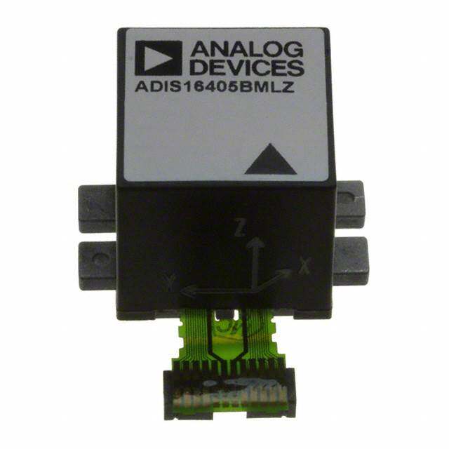
| 产品图片 |
|
| rohs | RoHS 合规性豁免无铅 / 符合限制有害物质指令(RoHS)规范要求 |
| 产品系列 | 螺旋仪,Analog Devices ADIS16375BMLZiSensor™ |
| 数据手册 | |
| 产品型号 | ADIS16375BMLZ |
| 产品种类 | 螺旋仪 |
| 传感器类型 | 加速计,陀螺仪,3 轴 |
| 加速 | +/- 18 g |
| 商标 | Analog Devices |
| 封装 | Bulk |
| 工厂包装数量 | 1 |
| 数字输出-总线接口 | SPI |
| 最大工作温度 | + 85 C |
| 最小工作温度 | - 40 C |
| 标准包装 | 1 |
| 灵敏度 | 0.01311 deg/s/LSB |
| 电源电压-最大 | 3.6 V |
| 电源电压-最小 | 3 V |
| 电源电流 | 173 mA |
| 系列 | ADIS16375 |
| 输出类型 | 数字 - SPI |


- 商务部:美国ITC正式对集成电路等产品启动337调查
- 曝三星4nm工艺存在良率问题 高通将骁龙8 Gen1或转产台积电
- 太阳诱电将投资9.5亿元在常州建新厂生产MLCC 预计2023年完工
- 英特尔发布欧洲新工厂建设计划 深化IDM 2.0 战略
- 台积电先进制程称霸业界 有大客户加持明年业绩稳了
- 达到5530亿美元!SIA预计今年全球半导体销售额将创下新高
- 英特尔拟将自动驾驶子公司Mobileye上市 估值或超500亿美元
- 三星加码芯片和SET,合并消费电子和移动部门,撤换高东真等 CEO
- 三星电子宣布重大人事变动 还合并消费电子和移动部门
- 海关总署:前11个月进口集成电路产品价值2.52万亿元 增长14.8%


PDF Datasheet 数据手册内容提取
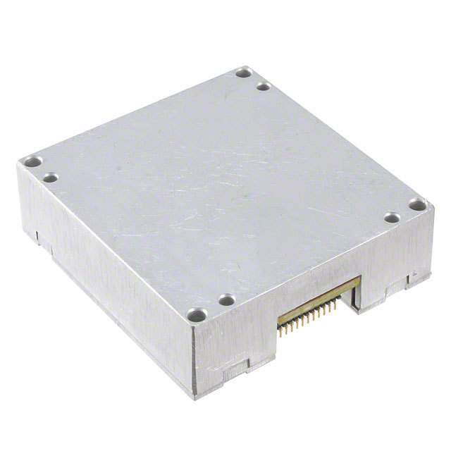
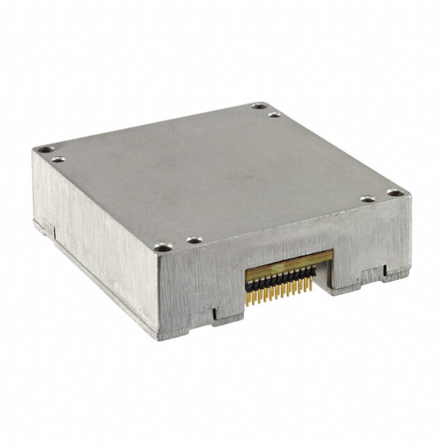
Low Profile, Low Noise Six Degrees of Freedom Inertial Sensor Data Sheet ADIS16375 FEATURES FUNCTIONAL BLOCK DIAGRAM Triaxis digital gyroscope, ±300°/sec TEMPERATURE Tight orthogonal alignment: 0.05° SENSOR Triaxis digital accelerometer: ±18 g TRIAXIS MEMS CS ANGULAR RATE Delta-angle/velocity calculations SENSOR SIGNAL CALIBRATION OUTPUT SCLK CONDITIONING AND REGISTERS Wide sensor bandwidth: 330 Hz AND DIGITAL AND SPI DIN CONVERSION INTERFACE High sample rate: 2.460 kSPS PROCESSING DOUT Autonomous operation and data collection TRIAXIS MEMS No external configuration commands required ACCELERATION SENSOR Startup time: 500 ms VDDRTC ALARMS Factory calibrated sensitivity, bias, and axial alignment POWER VCC Calibration temperature range: −40°C to +85°C MANAGEMENT SELF-TEST DIGITAL SPI-compatible serial interface CONTROL GND Embedded temperature sensor ADIS16375 ProAgurtaommmataicb laen odp meraantuioanl bainads ccoonrrtercotli on controls RST DIO1 DIO2 DIO3 DIO4 09389-001 4 FIR filter banks, 120 configurable taps Figure 1. Digital I/O: data-ready, alarm indicator, external clock GENERAL DESCRIPTION Alarms for condition monitoring The ADIS16375 iSensor® is a complete inertial system that includes Power-down/sleep mode for power management a triaxis gyroscope and triaxis accelerometer. Each sensor in the Enable external sample clock input: up to 2.25 kHz ADIS16375 combines industry-leading iMEMS® technology Single-command self test with signal conditioning that optimizes dynamic performance. Single-supply operation: 3.3 V The factory calibration characterizes each sensor for sensitivity, 2000 g shock survivability bias, alignment, and linear acceleration (gyro bias). As a result, Operating temperature range: −40°C to +105°C each sensor has its own dynamic compensation formulas that provide accurate sensor measurements over a temperature APPLICATIONS range of −40°C to +105°C. Precision instrumentation The ADIS16375 provides a simple, cost-effective method for Platform stabilization and control integrating accurate, multiaxis, inertial sensing into industrial Industrial vehicle navigation systems, especially when compared with the complexity and Downhole instrumentation investment associated with discrete designs. All necessary motion Robotics testing and calibration are part of the production process at the factory, greatly reducing system integration time. Tight orthogonal alignment simplifies inertial frame alignment in navigation systems. An improved SPI interface and register structure provide faster data collection and configuration control. This compact module is approximately 44 mm × 47 mm × 14 mm and provides a flexible connector interface that enables multiple mounting orientation options. Rev. D Document Feedback Information furnished by Analog Devices is believed to be accurate and reliable. However, no responsibility is assumed by Analog Devices for its use, nor for any infringements of patents or other One Technology Way, P.O. Box 9106, Norwood, MA 02062-9106, U.S.A. rights of third parties that may result from its use. Specifications subject to change without notice. No license is granted by implication or otherwise under any patent or patent rights of Analog Devices. Tel: 781.329.4700 ©2010–2017 Analog Devices, Inc. All rights reserved. Trademarks and registered trademarks are the property of their respective owners. Technical Support www.analog.com
ADIS16375 Data Sheet TABLE OF CONTENTS Features .............................................................................................. 1 Digital Signal Processing ............................................................... 18 Applications ....................................................................................... 1 Sampling Plan ............................................................................. 18 Functional Block Diagram .............................................................. 1 Averaging/Decimation Filter .................................................... 18 General Description ......................................................................... 1 FIR Filter Banks .......................................................................... 18 Revision History ............................................................................... 3 Calibration ....................................................................................... 20 Specifications ..................................................................................... 4 Alarms .............................................................................................. 23 Timing Specifications .................................................................. 6 System Controls .............................................................................. 24 Absolute Maximum Ratings ............................................................ 7 Global Commands ..................................................................... 24 ESD Caution .................................................................................. 7 Memory Management ............................................................... 24 Pin Configuration and Function Descriptions ............................. 8 General-Purpose I/O ................................................................. 25 Typical Performance Characteristics ............................................. 9 Power Management.................................................................... 25 Basic Operation............................................................................... 10 Applications Information .............................................................. 27 Register Structure ....................................................................... 10 Mounting Tips ............................................................................ 27 SPI Communication ................................................................... 11 Evaluation Tools ......................................................................... 27 Device Configuration ................................................................ 11 Power Supply Considerations ................................................... 27 Reading Sensor Data .................................................................. 11 Outline Dimensions ....................................................................... 28 User Registers .................................................................................. 12 Ordering Guide .......................................................................... 28 Output Data Registers .................................................................... 14 Rev. D | Page 2 of 28
Data Sheet ADIS16375 REVISION HISTORY 10/2017—Rev. C to Rev. D 7/2011—Rev. A to Rev. B Changes to Logic 0 Input Current, I Parameter, Table 1 ........... 4 Changes to Accelerometers, Nonlinearity Parameter and Power IL Added Note 3, Table 1; Renumbered Sequentially ....................... 5 Supply, VDD Parameter in Table 1 ................................................. 3 Deleted Prototype Interface Board Section, Table 99, and Changes to t , t , t, and t Parameters in Table 2.................... 5 CLS CHS 2 3 Installation Tips Section; Renumbered Sequentially .................. 26 Changed Angular Displacement Heading to Delta Angles ....... 14 Replaced Figure 23 .......................................................................... 27 Changes to Delta Angles Section .................................................. 14 Changes to Figure 24 and Figure 25 ............................................. 27 Changes to Table 28 and Velocity Changes Section ................... 15 Added Mounting Tips Section, Evaluation Tools Section, Change to Figure 18 ........................................................................ 17 Breakout Board, ADIS16IMU/PCBZ Section, PC-Based Changes to Data-Ready Indicator Section and Input Sync/Clock Evaluation, EVAL-ADIS2 Section, and Power Supply Control Section................................................................................ 24 Considerations Section ................................................................... 27 Moved Real-Time Clock Configuration/Data Section, Table 96, Table 97, and Table 98..................................................................... 25 8/2012—Rev. B to Rev. C Changes to Real-Time Clock Configuration/Data Section ....... 25 Changes to Features Section and General Description Section .. 1 Changes to Prototype Interface Board Section ........................... 26 Changes to Table 2 ............................................................................ 5 Changes to Table 3 ............................................................................ 6 2/2011—Rev. 0 to Rev. A Changes to Basic Operation Section ............................................... 9 Changes to Gyroscopes Misalignment and Accelerometers Changes to Dual Memory Structure Section ............................... 10 Misalignment Test Conditions/Comments, Table 1 ..................... 3 Changes to Acceleration Section and Delta Angles Section...... 14 Added Endnote 7 .............................................................................. 4 Changes to Figure 18 ...................................................................... 17 Changes to Table 54 and Table 55 ................................................. 17 Changes to Table 71 to Table 76 .................................................... 20 Changes to Table 57, Table 58, and Table 59 ............................... 18 Changes to Restoring Factory Calibration Section, Linear Acceleration on Effect on Gyroscope Bias Section, and Point of 10/2010—Revision 0: Initial Version Percussion Alignment Section ....................................................... 21 Changes to Table 88 ........................................................................ 22 Changes to Automatic Self Test Section, Memory Management Section, and Flash Memory Test Section ..................................... 23 Changes to General Purpose I/O Control Section ..................... 24 Changes to Real-Time Clock Configuration/Data Section ....... 25 Changes to Prototype Interface Board and Figure 23 ................ 26 Updated Outline Dimensions ........................................................ 28 Changes to Ordering Guide ........................................................... 28 Rev. D | Page 3 of 28
ADIS16375 Data Sheet SPECIFICATIONS T = 25°C, VDD = 3.3 V, angular rate = 0°/sec, dynamic range = ±300°/sec ± 1 g, unless otherwise noted. A Table 1. Parameter Test Conditions/Comments Min Typ Max Unit GYROSCOPES Dynamic Range ±300 ±350 °/sec Sensitivity1 16-bit resolution, x_GYRO_OUT registers only 0.01311 °/sec/LSB Initial Sensitivity Tolerance ±1 % Sensitivity Temperature Coefficient −40°C ≤ T ≤ +85°C ±40 ppm/°C A Misalignment Axis-to-axis ±0.05 Degrees Axis-to-frame (package) ±1.0 Degrees Nonlinearity Best-fit straight line ±0.025 % of FS Initial Bias Error ±1 σ ±1.0 °/sec In-Run Bias Stability 1 σ 12 °/hr Angular Random Walk 1 σ 1.0 °/√hr Bias Temperature Coefficient −40°C ≤ T ≤ +85°C ±0.005 °/sec/°C A Linear Acceleration Effect on Bias Any axis, 1 σ (GEN_CONFIG[7] = 1) ±0.013 °/sec/g Output Noise No filtering 0.45 °/sec rms Rate Noise Density f = 25 Hz, no filtering 0.02 °/sec/√Hz rms 3 dB Bandwidth 330 Hz Sensor Resonant Frequency 14.5 kHz ACCELEROMETERS Each axis Dynamic Range ±18 g Sensitivity1 16-bit resolution, x_ACCL_OUT registers only 0.8192 mg/LSB Initial Sensitivity Tolerance ±1 % Sensitivity Temperature Coefficient −40°C ≤ T ≤ +85°C ±25 ppm/°C A Misalignment Axis-to-axis ±0.035 Degrees Axis-to-frame (package) ±1.0 Degrees Nonlinearity Best-fit straight line, ±10 g ±0.1 % of FS Best-fit straight line, ±18 g ±0.5 % of FS Initial Bias Error ±1 σ ±16 mg In-Run Bias Stability 1 σ 0.13 mg Velocity Random Walk 1 σ 0.076 m/sec/√hr Bias Temperature Coefficient −40°C ≤ T ≤ +85°C ±0.1 mg/°C A Output Noise No filtering 1.5 mg rms Noise Density No filtering 0.06 mg/√Hz rms 3 dB Bandwidth 330 Hz Sensor Resonant Frequency 5.5 kHz TEMPERATURE SENSOR Scale Factor Output = 0x0000 at 25°C (±5°C) 0.00565 °C/LSB LOGIC INPUTS2 Input High Voltage, V 2.0 V IH Input Low Voltage, V 0.8 V IL CS Wake-Up Pulse Width 20 µs Logic 1 Input Current, I V = 3.3 V 10 µA IH IH Logic 0 Input Current, I V = 0 V IL IL All Pins Except RST, CS 10 µA RST, CS Pins3 0.33 mA Input Capacitance, C 10 pF IN DIGITAL OUTPUTS Output High Voltage, V I = 0.5 mA 2.4 V OH SOURCE Output Low Voltage, V I = 2.0 mA 0.4 V OL SINK Rev. D | Page 4 of 28
Data Sheet ADIS16375 Parameter Test Conditions/Comments Min Typ Max Unit FLASH MEMORY Endurance4 100,000 Cycles Data Retention5 T = 85°C 20 Years J FUNCTIONAL TIMES6 Time until data is available Power-On Startup Time 500 ms Reset Recovery Time 500 ms Sleep Mode Recovery Time 500 µs Flash Memory Update Time 375 ms Flash Memory Test Time 50 ms Automatic Self Test Time Using internal clock, 100 SPS 10 ms CONVERSION RATE 2.46 kSPS Initial Clock Accuracy 0.02 % Temperature Coefficient 40 ppm/°C Sync Input Clock 0.77 2.25 kHz POWER SUPPLY, VDD Operating voltage range 3.0 3.6 V Power Supply Current8 Normal mode, VDD = 3.3 V 173 mA Sleep mode, VDD = 3.3 V 12.3 mA Power-down mode, VDD = 3.3 V 120 µA POWER SUPPLY, VDDRTC Operating voltage range 3.3 V Real-Time Clock Supply Current Normal mode, VDDRTC = 3.3 V 13 µA 1 Each gyroscope and accelerometer has 32 bits of available resolution. The 16-bit sensitivity shown reflects the register that contains the upper 16 bits of the sensor output. Divide this number by 2 for every bit added to this resolution in downstream processing routines. 2 The digital I/O signals are driven by an internal 3.3 V supply, and the inputs are 5 V tolerant. 3 RST and CS pins are connected to the VDD pin through 10 kΩ pull-up resistors. 4 Endurance is qualified as per JEDEC Standard 22, Method A117, and measured at −40°C, +25°C, +85°C, and +125°C. 5 The data retention lifetime equivalent is at a junction temperature (TJ) of 85°C as per JEDEC Standard 22, Method A117. Data retention lifetime decreases with junction temperature. 6 These times do not include thermal settling and internal filter response times (330 Hz bandwidth), which may affect overall accuracy. 7 The 0.7 kHz lower limit is established to support Nyquist sampling criteria for the 330 Hz sensor bandwidth. 8 During startup, the power supply current increases and experiences transient behaviors for a period of 400 µs. The peak current during the 400 µs transient period can reach 1500 mA. Rev. D | Page 5 of 28
ADIS16375 Data Sheet TIMING SPECIFICATIONS T = 25°C, VDD = 3.3 V, unless otherwise noted. A Table 2. Normal Mode Parameter Description Min1 Typ Max Unit f Serial clock 0.01 15 MHz SCLK t Stall period between data 2 µs STALL t Serial clock low period 31 ns CLS t Serial clock high period 31 ns CHS t Chip select to clock edge 32 ns CS t DOUT valid after SCLK edge 10 ns DAV t DIN setup time before SCLK rising edge 2 ns DSU t DIN hold time after SCLK rising edge 2 ns DHD t , t DOUT rise/fall times, ≤100 pF loading 3 8 ns DR DF tDSOE CS assertion to data out active 0 11 ns t SCLK edge to data out invalid 0 ns HD tSFS Last SCLK edge to CS deassertion 32 ns tDSHI CS deassertion to data out high impedance 0 9 ns t Input sync pulse width 5 µs 1 t Input sync to data-ready output 430 µs 2 t Input sync period 440 µs 3 1 Guaranteed by design and characterization but not tested in production. Timing Diagrams CS tCS tCHS tCLS tSFS 1 2 3 4 5 6 15 16 SCLK tDSOE tDAV tHD tDSHI DOUT MSB DB14 DB13 DB12 DB11 DB10 DB2 DB1 LSB tDSU tDHD DIN R/W A6 A5 A4 A3 A2 D2 D1 LSB 09389-002 Figure 2. SPI Timing and Sequence tSTALL CS SCLK 09389-003 Figure 3. Stall Time and Data Rate t3 t2 t1 SYNC CLOCK (CLKIN) DATA READY REGOISUTTEPRUST DATA VALID DATA VALID 09389-004 Figure 4. Input Clock Timing Diagram Rev. D | Page 6 of 28
Data Sheet ADIS16375 ABSOLUTE MAXIMUM RATINGS Table 3. Stresses above those listed under Absolute Maximum Ratings Parameter Rating may cause permanent damage to the device. This is a stress Acceleration rating only; functional operation of the device at these or any Any Axis, Unpowered 2000 g other conditions above those indicated in the operational Any Axis, Powered 2000 g section of this specification is not implied. Exposure to absolute VCC to GND −0.3 V to +3.6 V maximum rating conditions for extended periods may affect Digital Input Voltage to GND −0.3 V to VCC + 0.2 V device reliability. Digital Output Voltage to GND −0.3 V to VCC + 0.2 V Table 4. Package Characteristics Operating Temperature Range −40°C to +105°C Package Type θ θ Device Weight Storage Temperature Range −65°C to +150°C1 JA JC 24-Lead Module (ML-24-6) 20.5 6.3 25 g 1 Extended exposure to temperatures outside the specified temperature range of −40°C to +105°C can adversely affect the accuracy of the factory calibration. For best accuracy, store the parts within the specified operating range of −40°C to +105°C. ESD CAUTION Rev. D | Page 7 of 28
ADIS16375 Data Sheet PIN CONFIGURATION AND FUNCTION DESCRIPTIONS ADIS16375 TOP VIEW (Not to Scale) DNC DNC DNC DNC DNC GND VDD VDD RST CS DOUT DIO4 24 22 20 18 16 14 12 10 8 6 4 2 23 21 19 17 15 13 11 9 7 5 3 1 C C C C D D D 2 1 N K 3 DRT DN DN DN GN GN VD DIO DIO DI SCL DIO D V NOTES 1. THIS REPRESENTATION DISPLAYS THE TOP VIEW PINOUT FOR THE MATING SOCKET CONNECTOR. 2. THE ACTUAL CONNECTOR PINS ARE NOT VISIBLE FROM 34 .. DMTHNAECT IT=NO GDP OC V ONIENOWNTE .CCOTNONRE: CSTA.MTEC CLM-112-02 OR EQUIVALENT. 09389-005 Figure 5. Mating Connector Pin Assignments PIN 23PIN 1 09389-006 Figure 6. Axial Orientation (Top Side Facing Up) Table 5. Pin Function Descriptions Pin No. Mnemonic Type Description 1 DIO3 Input/Output Configurable Digital Input/Output. 2 DIO4 Input/Output Configurable Digital Input/Output. 3 SCLK Input SPI Serial Clock. 4 DOUT Output SPI Data Output. Clocks output on SCLK falling edge. 5 DIN Input SPI Data Input. Clocks input on SCLK rising edge. 6 CS Input SPI Chip Select. 7 DIO1 Input/Output Configurable Digital Input/Output. 8 RST Input Reset. 9 DIO2 Input/Output Configurable Digital Input/Output. 10, 11, 12 VDD Supply Power Supply. 13, 14, 15 GND Supply Power Ground. 16 to 22, 24 DNC Not applicable Do Not Connect. 23 VDDRTC Supply Real-Time Clock Power Supply. Rev. D | Page 8 of 28
Data Sheet ADIS16375 TYPICAL PERFORMANCE CHARACTERISTICS 1000 0.001 AVERAGE AVERAGE +1σ LAN VARIANCE (°/Hour) 10100 +1σ ALLAN VARIANCE (g)0.0001 –1σ L A –1σ 10.01 0.1 INTEG1RATION P1E0RIOD (S1e0c0onds) 1000 10000 09389-007 0.000010.01 0.1 INTEG1RATION P1E0RIOD (S1e0c0onds) 1000 10000 09389-008 Figure 7. Gyroscope Allan Variance, +25°C Figure 8. Accelerometer Allan Variance, 25°C Rev. D | Page 9 of 28
ADIS16375 Data Sheet BASIC OPERATION The ADIS16375 is an autonomous sensor system that starts up REGISTER STRUCTURE on its own when it has a valid power supply. After running through The register structure and SPI port provide a bridge between its initialization process, it begins sampling, processing, and the sensor processing system and an external, master processor. loading calibrated sensor data into the output registers, which It contains both output data and control registers. The output are accessible using the SPI port. The SPI port typically connects to data registers include the latest sensor data, a real-time clock, error a compatible port on an embedded processor, using the connection flags, alarm flags, and identification data. The control registers diagram in Figure 9. The four SPI signals facilitate synchronous, include sample rate, filtering, input/output, alarms, calibration, serial data communication. Connect RST (see Table 5) to a digital and diagnostic configuration options. All communication I/O line for remote reset control or leave it open for normal between the ADIS16375 and an external processor involves operation. The factory default configuration provides users either reading or writing to one of the user registers. with a data-ready signal on the DIO2 pin, which pulses high when new data is available in the output data registers. TRIAXIS OUTPUT I/O LINES ARE COMPATIBLE WITH GYRO DSP REGISTERS 3.3V LOGIC LEVELS +3.3V TRIAXIS PI VDD ACCEL S CONTROL SPYRSOTCEEMSSOR SS 6 CS10 11ADIS121637253 SETNEMSOPR CONTROLLER REGISTERS 09389-011 SPI MASTER Figure 10. Basic Operation SCLK 3 SCLK The register structure uses a paged addressing scheme that is MOSI 5 DIN comprised of 13 pages, with each one containing 64 register MISO 4 DOUT locations. Each register is 16-bits wide, with each byte having its IRQ 9 DIO2 own unique address within that page’s memory map. The SPI 13 14 15 port has access to one page at a time, using the bit sequences in 09389-010 Fcoigduer teo 1 t5h. eS PelAecGtE th_IeD p argege itsote ar.c tRiveaatde tfhoer PSAPIG aEc_ceIDss rbeyg wistreitri ntog its Figure 9. Electrical Connection Diagram determine which page is currently active. Table 8 displays the Table 6. Generic Master Processor Pin Names and Functions PAGE_ID contents for each page, along with their basic function. Mnemonic Function The PAGE_ID register is located at Address 0x00 on every page. SS Slave select Table 8. User Register Page Assignments IRQ Interrupt request Page PAGE_ID Function MOSI Master output, slave input 0 0x00 Output data, clock, identification MISO Master input, slave output 1 0x01 Reserved SCLK Serial clock 2 0x02 Calibration Embedded processors typically use control registers to configure 3 0x03 Control: sample rate, filtering, I/O, alarms their serial ports for communicating with SPI slave devices, 4 0x04 Reserved such as the ADIS16375. Table 7 provides a list of settings, which 5 0x05 FIR Filter Bank A Coefficients, 1 to 60 describe the SPI protocol of the ADIS16375. The initialization 6 0x06 FIR Filter Bank A, Coefficients, 61 to 120 routine of the master processor typically establishes these settings 7 0x07 FIR Filter Bank B, Coefficients, 1 to 60 using firmware commands to write them into its serial control 8 0x08 FIR Filter Bank B, Coefficients, 61 to 120 registers. 9 0x09 FIR Filter Bank C, Coefficients, 1 to 60 10 0x0A FIR Filter Bank C, Coefficients, 61 to 120 Table 7. Generic Master Processor SPI Settings 11 0x0B FIR Filter Bank D, Coefficients, 1 to 60 Processor Setting Description 12 0x0C FIR Filter Bank D, Coefficients, 61 to 120 Master The ADIS16375 operates as a slave. SCLK ≤ 15 MHz Maximum serial clock rate. SPI Mode 3 CPOL = 1 (polarity), and CPHA = 1 (phase). MSB-First Mode Bit sequence. 16-Bit Mode Shift register/data length. Rev. D | Page 10 of 28
Data Sheet ADIS16375 SPI COMMUNICATION MANUAL The SPI port supports full duplex communication, as shown in FLASH BACKUP Figure 15, which enables external processors to write to DIN while reading DOUT, if the previous command was a read NONVOLATILE VOLATILE FLASH MEMORY SRAM request. Figure 15 provides a guideline for the bit coding on (NO SPI ACCESS) SPI ACCESS both DIN and DOUT. START-UP DThEeV SIPCI Ep rCoOvidNeFs IwGrUiteR aAccTeIsOs tNo the control registers, one byte at RESET 09389-013 Figure 12. SRAM and Flash Memory Diagram a time, using the bit assignments shown in Figure 15. Each register READING SENSOR DATA has 16 bits, where Bits[7:0] represent the lower address (listed in Table 9) and Bits[15:8] represent the upper address. Write to the The ADIS16375 automatically starts up and activates Page 0 for lower byte of a register first, followed by a write to its upper byte data register access. Write 0x00 to the PAGE_ID register (DIN = second. The only register that changes with a single write to its 0x8000) to activate Page 0 for data access after accessing any other lower byte is the PAGE_ID register. For a write command, the page. A single register read requires two 16-bit SPI cycles. The first first bit in the DIN sequence is set to 1. The Address Bits[A6:A0] cycle requests the contents of a register using the bit assignments in represent the target address and the Data Command Bits[DC7:DC0] Figure 15, and then the register contents flow out of DOUT during represent the data being written to the location. Figure 11 the second sequence. The first bit in a DIN command is zero, provides an example of writing 0x03 to Address 0x00 followed by either the upper or lower address for the register. (PAGE_ID[7:0]), using DIN = 0x8003. This write command The last eight bits are don’t care, but the SPI requires the full set activates the control page for SPI access. of 16 SCLKs to receive the request. Figure 13 includes two register reads in succession, which starts with DIN = 0x1A00 to request CS the contents of the Z_GYRO_OUT register and follows with 0x1800 to request the contents of the Z_GYRO_LOW register. SCLK DFDINiIgN =u r1e0 0101 0. 0S0P0I 0S0e0q0u 0e0n1c1e = f o0xr8 A0c0t3i,v WatRinITgE tSh 0ex C03o nTOtr oAlD PDaRgEeS (SD 0INx0 =0 0x8003) 09389-012 DODUINT 0x1A00 Z_G0YxR1O80_0OUT Z_AGDYNDREROXE_TSLSOW 09389-014 Dual Memory Structure Figure 13. SPI Read Example Writing configuration data to a control register updates its SRAM Figure 14 provides an example of the four SPI signals when reading contents, which are volatile. After optimizing each relevant control PROD_ID in a repeating pattern. This is a good pattern to use register setting in a system, use the manual flash update command, for troubleshooting the SPI interface setup and communications which is located in GLOB_CMD[3] on Page 3 of the register map. because the contents of PROD_ID are predefined and stable. Activate the manual flash update command by turning to Page 3 CS (DIN = 0x8003) and setting GLOB_CMD[3] = 1 (DIN = 0x8204, then DIN = 0x8300). Make sure that the power supply is within SCLK specification for the entire 375 ms processing time for a flash DIN DIN = 0111 1110 0000 0000 = 0x7E00 memory update. Table 9 provides a memory map for all of the ususperp orergt iasstesorsc,i awthedic wh iitnhc leuadcehs r ae gciosltuerm. An fyoers tihne t fhliass hco bluacmknu p DOUT DOUT = 0011 1111 1111 0111 = 0x3FF7 = 16,375 (PROD_ID) 09389-015 indicates that a register has a mirror location in flash and, when Figure 14. SPI Read Example, Second 16-Bit Sequence backed up properly, automatically restores itself during startup or after a reset. Figure 12 provides a diagram of the dual memory structure used to manage operation and store critical user settings. CS SCLK DIN R/W A6 A5 A4 A3 A2 A1 A0 DC7 DC6 DC5 DC4 DC3 DC2 DC1 DC0 R/W A6 A5 DOUT D15 D14 D13 D12 D11 D10 D9 D8 D7 D6 D5 D4 D3 D2 D1 D0 D15 D14 D13 NOTES 12..FWDOOHRUE TNO BTCIHSTE SIRS A DHREIEGV HPICR, EDOSOD.UUTC EISD I NO NAL TYH WREHEE-NS TTAHTEE P, RHEIGVHIO IUMSP E16D-ABNITC DEI NM OSEDQE,U WENHCICEH S ATLALROTWS SW MITUHL RT/IWFU =N C0.TIONAL USE OF THE LINE 09389-016 Figure 15. SPI Communication Bit Sequence Rev. D | Page 11 of 28
ADIS16375 Data Sheet USER REGISTERS Table 9. User Register Memory Map (N/A = Not Applicable) Name R/W Flash PAGE_ID Address Default Register Description Format PAGE_ID R/W No 0x00 0x00 0x00 Page Identifier N/A Reserved N/A N/A 0x00 0x02 to 0x07 N/A Reserved N/A SYS_E_FLAG R No 0x00 0x08 0x0000 Output, system error flags Table 41 DIAG_STS R No 0x00 0x0A 0x0000 Output, self test error flags Table 42 ALM_STS R No 0x00 0x0C 0x0000 Output, alarm error flags Table 43 TEMP_OUT R No 0x00 0x0E N/A Output, temperature Table 39 X_GYRO_LOW R No 0x00 0x10 N/A Output, x-axis gyroscope, low word Table 15 X_GYRO_OUT R No 0x00 0x12 N/A Output, x-axis gyroscope, high word Table 11 Y_GYRO_LOW R No 0x00 0x14 N/A Output, y-axis gyroscope, low word Table 16 Y_GYRO_OUT R No 0x00 0x16 N/A Output, y-axis gyroscope, high word Table 12 Z_GYRO_LOW R No 0x00 0x18 N/A Output, z-axis gyroscope, low word Table 17 Z_GYRO_OUT R No 0x00 0x1A N/A Output, z-axis gyroscope, high word Table 13 X_ACCL_LOW R No 0x00 0x1C N/A Output, x-axis accelerometer, low word Table 22 X_ACCL_OUT R No 0x00 0x1E N/A Output, x-axis accelerometer, high word Table 18 Y_ACCL_LOW R No 0x00 0x20 N/A Output, y-axis accelerometer, low word Table 23 Y_ACCL_OUT R No 0x00 0x22 N/A Output, y-axis accelerometer, high word Table 19 Z_ACCL_LOW R No 0x00 0x24 N/A Output, z-axis accelerometer, low word Table 24 Z_ACCL_OUT R No 0x00 0x26 N/A Output, z-axis accelerometer, high word Table 20 Reserved N/A N/A 0x00 0x28 to 0x3F N/A Reserved N/A X_DELTA_ANG_L R No 0x00 0x40 N/A Output, x-axis delta angle, low word Table 29 X_DELTA_ANG_H R No 0x00 0x42 N/A Output, x-axis delta angle, high word Table 25 Y_DELTA_ANG_L R No 0x00 0x44 N/A Output, y-axis delta angle, low word Table 30 Y_DELTA_ANG_H R No 0x00 0x46 N/A Output, y-axis delta angle, high word Table 26 Z_DELTA_ANG_L R No 0x00 0x48 N/A Output, z-axis delta angle, low word Table 31 Z_DELTA_ANG_H R No 0x00 0x4A N/A Output, z-axis delta angle, high word Table 27 X_DELTA_VEL_L R No 0x00 0x4C N/A Output, x-axis delta velocity, low word Table 36 X_DELTA_VEL_H R No 0x00 0x4E N/A Output, x-axis delta velocity, high word Table 32 Y_DELTA_VEL_L R No 0x00 0x50 N/A Output, y-axis delta velocity, low word Table 37 Y_DELTA_VEL_H R No 0x00 0x52 N/A Output, y-axis a delta velocity, high word Table 33 Z_DELTA_VEL_L R No 0x00 0x54 N/A Output, z-axis delta velocity, low word Table 38 Z_DELTA_VEL_H R No 0x00 0x56 N/A Output, z-axis delta velocity, high word Table 34 Reserved N/A N/A 0x00 0x58 to 0x6F N/A Reserved N/A TIME_MS_OUT R/W Yes 0x00 0x70 N/A Output, time, minutes, and seconds Table 96 TIME_DH_OUT R/W Yes 0x00 0x72 N/A Output, time, days, and hours Table 97 TIME_YM_OUT R/W Yes 0x00 0x74 N/A Output, time, years, and months Table 98 Reserved N/A N/A 0x00 0x76 N/A Reserved N/A LOT_ID1 R Yes 0x00 0x78 N/A Output, lot identification number Table 44 LOT_ID2 R Yes 0x00 0x7A N/A Output, lot identification number Table 45 LOT_ID3 R Yes 0x00 0x7C N/A Output, lot identification number Table 46 PROD_ID R Yes 0x00 0x7E 0x3FF7 Output, product identification (16,375) Table 47 Reserved N/A N/A 0x01 0x00 to 0x7F N/A Reserved N/A PAGE_ID R/W No 0x02 0x00 0x00 Page identifier N/A Reserved N/A N/A 0x02 0x02 to 0x0E N/A Reserved N/A XGYRO_OFF_L R/W Yes 0x02 0x10 0x0000 Calibration, offset, x-axis gyroscope, low word Table 62 XGYRO_OFF_H R/W Yes 0x02 0x12 0x0000 Calibration, offset, x-axis gyroscope, high word Table 59 YGYRO_OFF_L R/W Yes 0x02 0x14 0x0000 Calibration, offset, y-axis gyroscope, low word Table 63 YGYRO_OFF_H R/W Yes 0x02 0x16 0x0000 Calibration, offset, y-axis gyroscope, high word Table 60 ZGYRO_OFF_L R/W Yes 0x02 0x18 0x0000 Calibration, offset, z-axis gyroscope, low word Table 64 ZGYRO_OFF_H R/W Yes 0x02 0x1A 0x0000 Calibration, offset, z-axis gyroscope, high word Table 61 XACCL_OFF_L R/W Yes 0x02 0x1C 0x0000 Calibration, offset, x-axis accelerometer, low word Table 68 XACCL_OFF_H R/W Yes 0x02 0x1E 0x0000 Calibration, offset, x-axis accelerometer, high word Table 65 Rev. D | Page 12 of 28
Data Sheet ADIS16375 Name R/W Flash PAGE_ID Address Default Register Description Format YACCL_OFF_L R/W Yes 0x02 0x20 0x0000 Calibration, offset, y-axis accelerometer, low word Table 69 YACCL_OFF_H R/W Yes 0x02 0x22 0x0000 Calibration, offset, y-axis accelerometer, high word Table 66 ZACCL_OFF_L R/W Yes 0x02 0x24 0x0000 Calibration, offset, z-axis accelerometer, low word Table 70 ZACCL_OFF_H R/W Yes 0x02 0x26 0x0000 Calibration, offset, z-axis accelerometer, high word Table 67 Reserved N/A N/A 0x02 0x28 to 0x3E N/A Reserved N/A XGYRO_SCL R/W Yes 0x02 0x40 0x0000 Calibration, scale, x-axis gyroscope Table 71 YGYRO_SCL R/W Yes 0x02 0x42 0x0000 Calibration, scale, y-axis gyroscope Table 72 ZGYRO_SCL R/W Yes 0x02 0x44 0x0000 Calibration, scale, z-axis gyroscope Table 73 XACCL_SCL R/W Yes 0x02 0x46 0x0000 Calibration, scale, x-axis accelerometer Table 74 YACCL_SCL R/W Yes 0x02 0x48 0x0000 Calibration, scale, y-axis accelerometer Table 75 ZACCL_SCL R/W Yes 0x02 0x4A 0x0000 Calibration, scale, z-axis accelerometer Table 76 Reserved N/A N/A 0x02 0x4C to 0x67 N/A Reserved N/A SERIAL_NUM R Yes 0x02 0x68 N/A Serial number Table 48 Reserved N/A N/A 0x02 0x6Ato 0x77 N/A Reserved N/A FLSH_CNT_L R Yes 0x02 0x78 N/A Diagnostic, flash memory write count, low word Table 91 FLSH_CNT_H R Yes 0x02 0x7A N/A Diagnostic, flash memory write count, high word Table 92 Reserved N/A N/A 0x02 0x7C to 0x7F N/A Reserved N/A PAGE_ID R/W No 0x03 0x00 0x0000 Page identifier N/A GLOB_CMD W No 0x03 0x02 N/A Control, global commands Table 90 Reserved N/A N/A 0x03 0x04 N/A Reserved N/A FNCIO_CTRL R/W Yes 0x03 0x06 0x000D Control, I/O pins, functional definitions Table 93 GPIO_CTRL R/W Yes 0x03 0x08 0x0000 Control, I/O pins, general purpose Table 94 GEN_CONFIG R/W Yes 0x03 0x0A 0x00C0 Control, clock and miscellaneous correction Table 78 DEC_RATE R/W Yes 0x03 0x0C Control, output sample rate decimation Table 50 NULL_CFG R/W Yes 0x03 0x0E 0x070B Control, automatic bias correction configuration Table 77 SLP_CFG R/W No 0x03 0x10 N/A Control, power-down/sleep mode Table 95 Reserved N/A N/A 0x03 0x12 to 0x15 N/A Reserved N/A FILTER_SEL1 R/W Yes 0x03 0x16 0x0000 Filter selection Table 51 FILTER_SEL2 R/W Yes 0x03 0x18 0x0000 Filter selection Table 52 Reserved N/A N/A 0x03 0x1A to 0x1F N/A Reserved N/A ALM_CONFIG_1 R/W Yes 0x03 0x20 0x0000 Alarm configuration Table 86 ALM_CONFIG_2 R/W Yes 0x03 0x22 0x0000 Alarm configuration Table 87 Reserved N/A N/A 0x03 0x24 to 0x3E N/A Reserved N/A XG_ALM_MAG R/W Yes 0x03 0x40 0x0000 X-axis gyroscope alarm trigger level Table 80 YG_ALM_MAG R/W Yes 0x03 0x42 0x0000 Y-axis gyroscope alarm trigger level Table 81 ZG_ALM_MAG R/W Yes 0x03 0x44 0x0000 Z-axis gyroscope alarm trigger level Table 82 XA_ALM_MAG R/W Yes 0x03 0x46 0x0000 X-axis accelerometer alarm trigger level Table 83 YA_ALM_MAG R/W Yes 0x03 0x48 0x0000 Y-axis accelerometer alarm trigger level Table 84 ZA_ALM_MAG R/W Yes 0x03 0x4A 0x0000 Z-axis accelerometer alarm trigger level Table 85 Reserved N/A N/A 0x03 0x4C to 0x7F N/A Reserved N/A Reserved N/A N/A 0x04 0x00 to 0x7F N/A Reserved N/A FIR_COEF_Axxx R/W Yes 0x05 0x00 to 0x7F N/A FIR Filter Bank A, Coefficients 1 through 60 Table 53 FIR_COEF_Axxx R/W Yes 0x06 0x00 to 0x7F N/A FIR Filter Bank A, Coefficients 61 through 120 Table 53 FIR_COEF_Bxxx R/W Yes 0x07 0x00 to 0x7F N/A FIR Filter Bank B, Coefficients 1 through 60 Table 54 FIR_COEF_Bxxx R/W Yes 0x08 0x00 to 0x7F N/A FIR Filter Bank B, Coefficients 61 through 120 Table 54 FIR_COEF_Cxxx R/W Yes 0x09 0x00 to 0x7F N/A FIR Filter Bank C, Coefficients 1 through 60 Table 55 FIR_COEF_Cxxx R/W Yes 0x0A 0x00 to 0x7F N/A FIR Filter Bank C, Coefficients 61 through 120 Table 55 FIR_COEF_Dxxx R/W Yes 0x0B 0x00 to 0x7F N/A FIR Filter Bank D, Coefficients 1 through 60 Table 56 FIR_COEF_Dxxx R/W Yes 0x0C 0x00 to 0x7F N/A FIR Filter Bank D, Coefficients 61 through 120 Table 56 Rev. D | Page 13 of 28
ADIS16375 Data Sheet OUTPUT DATA REGISTERS After the ADIS16375 completes its startup process, the PAGE_ID X_GYRO_OUT X_GYRO_LOW rsfoetagrt iuSsPtse Iar na ccdoc npetsrasoi.d nPusa c0gtxe i 0d00e c0no0tn,i ftwiachianitcsio htn hs eer etosgu iPstaptegurets .0d aatsa ,t hreea al-cttiimvee p calgoec k, 15 X-AXIS GY0RO15SCOPE DATA 0 09389-017 Figure 16. Gyroscope Output Format, DEC_RATE > 0 Table 10. Output Data Register Summary The arrows in Figure 17 describe the direction of the motion, Register Address Measurement which produces a positive output response in each sensor’s SYS_E_FLAG 0x08 System flags output register. The accelerometers respond to both dynamic DIAG_STS 0x0A Self test flags and static forces associated with acceleration, including gravity. ALM_STS 0x0C Alarm flags When lying perfectly flat, as shown in Figure 17, the z-axis TEMP_OUT 0x0E Temperature accelerometer output is 1 g, and the x and y accelerometers is 0 g. X_GYRO_LOW 0x10 Gyroscope, X Z-AXIS X_GYRO_OUT 0x12 Gyroscope, X aZ Y_GYRO_LOW 0x14 Gyroscope, Y gZ Y_GYRO_OUT 0x16 Gyroscope, Y Z_GYRO_LOW 0x18 Gyroscope, Z X-AXIS Z_GYRO_OUT 0x1A Gyroscope, Z Y-AXIS X_ACCL_LOW 0x1C Accelerometer, X aY gX aX X_ACCL_OUT 0x1E Accelerometer, X Y_ACCL_LOW 0x20 Accelerometer, Y gY PIN 23PIN 1 09389-018 Y_ACCL_OUT 0x22 Accelerometer, Y Figure 17. Inertial Sensor Direction Reference Diagram Z_ACCL_LOW 0x24 Accelerometer, Z Rotation Rate (Gyroscope) Z_ACCL_OUT 0x26 Accelerometer, Z X_DELTA_ANG_L 0x40 Delta angle, X The registers that use the x_GYRO_OUT format are the primary X_DELTA_ANG_H 0x42 Delta angle, X registers for the gyroscope measurements. When processing data Y_DELTA_ANG_L 0x44 Delta angle, Y from these registers, use a 16-bit, twos complement data format. Y_DELTA_ANG_H 0x46 Delta angle, Y Table 11, Table 12 and Table 13 provide each register’s numerical Z_DELTA_ANG_L 0x48 Delta angle, Z format, and Table 14 provides x_GYRO_OUT digital coding Z_DELTA_ANG_H 0x4A Delta angle, Z examples. X_DELTA_VEL_L 0x4C Delta velocity, X Table 11. X_GYRO_OUT (Page 0, Base Address = 0x12) X_DELTA_VEL_H 0x4E Delta velocity, X Bits Description Y_DELTA_VEL_L 0x50 Delta velocity, Y [15:0] X-axis gyroscope data; twos complement, ±300°/sec Y_DELTA_VEL_H 0x52 Delta velocity, Y range, 0.013108°/sec per LSB, 0°/sec = 0x0000 Z_DELTA_VEL_L 0x54 Delta velocity, Z Z_DELTA_VEL_H 0x56 Delta velocity, Z Table 12. Y_GYRO_OUT (Page 0, Base Address = 0x16) TIME_MS_OUT 0x70 Time, min, and sec Bits Description TIME_DH_OUT 0x72 Time, day, and hour [15:0] Y-axis gyroscope data; twos complement, ±300°/sec TIME_YM_OUT 0x74 Time, year, and month range, 0.013108°/sec per LSB, 0°/sec = 0x0000 LOT_ID1 0x78 Lot identifier Table 13. Z_GYRO_OUT (Page 0, Base Address = 0x1A) LOT_ID2 0x7A Lot identifier Bits Description LOT_ID3 0x7C Lot identifier [15:0] Z-axis gyroscope data; twos complement, ±300°/sec PROD_ID 0x7E Product identifier range, 0.013108°/sec per LSB, 0°/sec = 0x0000 Inertial Sensor Data Format Table 14. x_GYRO_OUT Data Format Examples The gyroscope, accelerometer, delta angle, and delta velocity Rotation Rate Decimal Hex Binary output data use a 32-bit, twos complement format. Each output +300°/sec +22,887 0x5967 0101 1001 0110 0111 uses two registers to support this resolution. Figure 16 provides +0.026216/sec +2 0x0002 0000 0000 0000 0010 an example of how each register contributes to each inertial +0.013108°/sec +1 0x0001 0000 0000 0000 0001 measurement. In this case, X_GYRO_OUT is the most significant 0°/sec 0 0x0000 0000 0000 0000 0000 word (upper 16 bits), and X_GYRO_LOW is the least significant −0.013108°/sec −1 0xFFFF 1111 1111 1111 1111 word (lower 16 bits). In many cases, using the x_GYRO_OUT −0.026216°/sec −2 0xFFFE 1111 1111 1111 1110 registers alone provides sufficient resolution for preserving key −300°/sec −22,887 0xA699 1010 0110 1001 1001 performance metrics. Rev. D | Page 14 of 28
Data Sheet ADIS16375 The registers that use the x_GYRO_LOW naming format provide Table 22. X_ACCL_LOW (Page 0, Base Address = 0x1C) additional resolution for the gyroscope measurements. The Bits Description MSB has a weight of 0.006554°/sec, and each subsequent bit [15:0] X-axis accelerometer data; additional resolution bits carries a weight of ½ of the previous one. Table 23. Y_ACCL_LOW (Page 0, Base Address = 0x20) Table 15. X_GYRO_LOW (Page 0, Base Address = 0x10) Bits Description Bits Description [15:0] Y-axis accelerometer data; additional resolution bits [15:0] X-axis gyroscope data; additional resolution bits Table 24. Z_ACCL_LOW (Page 0, Base Address = 0x24) Table 16. Y_GYRO_LOW (Page 0, Base Address = 0x14) Bits Description Bits Description [15:0] Z-axis accelerometer data; additional resolution bits [15:0] Y-axis gyroscope data; additional resolution bits Delta Angles Table 17. Z_GYRO_LOW (Page 0, Base Address = 0x18) The delta angle outputs represent an integration of the gyroscope Bits Description measurements and use the following formula for all three axes [15:0] Z-axis gyroscope data; additional resolution bits (x-axis displayed): Acceleration ΔT ( ) Δθ = S × ω +ω The registers that use the x_ACCL_OUT format are the primary x 2 x,n+1 x,n registers for the accelerometer measurements. When processing where: data from these registers, use a 16-bit, twos complement data ω is the gyroscope, x-axis. x format. Table 18, Table 19 and Table 20 provide each register’s ΔT is the time between samples. S numerical format, and Table 21 provides x_ACCL_OUT digital DEC_RATE coding examples. ΔT = S f S Table 18. X_ACCL_OUT (Page 0, Base Address = 0x1E) When using the internal sample clock, f is equal to 2.46 kHz. Bits Description S When using the external clock option, the time between samples [15:0] X-axis accelerometer data; twos complement, ±18 g is the time between active edges on the input clock signal, as range, 0.8192 mg per LSB, 0 g = 0x0000 measured by the internal clock (252 MHz). See Table 50 for Table 19. Y_ACCL_OUT (Page 0, Base Address = 0x22) more information on the DEC_RATE register. The registers that Bits Description use the x_DELTA_ANG_H format are the primary registers for [15:0] Y-axis accelerometer data; twos complement, ±18 g the delta angle calculations. When processing data from these range, 0.8192 mg per LSB, 0 g = 0x0000 registers, use a 16-bit, twos complement data format. Table 25, Table 26, and Table 27 provide each register’s numerical format, Table 20. Z_ACCL_OUT (Page 0, Base Address = 0x26) and Table 28 provides several examples for converting digital Bits Description data into angular degrees (°). [15:0] Z-axis accelerometer data; twos complement, ±18 g range, 0.8192 mg per LSB, 0 g = 0x0000 Table 25. X_DELTA_ANG_H (Page 0, Base Address = 0x42) Table 21. x_ACCL_OUT Data Format Examples Bits Description Acceleration Decimal Hex Binary [15:0] X-axis delta angle data; twos complement, ±179.9891° range, sensitivity = 0.005493°/LSB, 0° = 0x0000 +18 g +21,973 0x55D5 0101 0101 1101 0101 +1.6384 mg +2 0x0002 0000 0000 0000 0010 Table 26. Y_DELTA_ANG_H (Page 0, Base Address = 0x46) +0.8192 mg +1 0x0001 0000 0000 0000 0001 Bits Description 0 mg 0 0x0000 0000 0000 0000 0000 [15:0] Y-axis delta angle data; twos complement, ±179.9891° −0.8192 mg −1 0xFFFF 1111 1111 1111 1111 range, sensitivity = 0.005493°/LSB, 0° = 0x0000 −1.6384 mg −2 0xFFFE 1111 1111 1111 1110 −18 g −21,973 0xAA2B 1010 1010 0010 1011 Table 27. Z_DELTA_ANG_H (Page 0, Base Address = 0x4A) Bits Description The registers that use the x_ACCL_LOW naming format provide [15:0] Z-axis delta angle data; twos complement, ±179.9891° additional resolution for the accelerometer measurements. The range, sensitivity = 0.005493°/LSB, 0° = 0x0000 MSB has a weight of 0.4096 mg, and each subsequent bit carries a weight of ½ of the previous one. Rev. D | Page 15 of 28
ADIS16375 Data Sheet Table 28. x_DELTA_ANG_H Data Format Examples Table 33. Y_DELTA_VEL_H (Page 0, Base Address = 0x52) Angle Decimal Hex Binary Bits Description +179.9891° +32,767 0x7FFF 0111 1111 1110 1111 [15:0] Y-axis delta velocity data; twos complement, +0.010986° +2 0x0002 0000 0000 0000 0010 ±99.998 m/sec, 3.0518 mm/sec per LSB, 0° = 0x0000 +0.005493° +1 0x0001 0000 0000 0000 0001 Table 34. Z_DELTA_VEL_H (Page 0, Base Address = 0x56) 0° 0 0x0000 0000 0000 0000 0000 Bits Description −0.005493° −1 0xFFFF 1111 1111 1111 1111 [15:0] Z-axis delta velocity data; twos complement, −0.010986° −2 0xFFFE 1111 1111 1111 1110 ±99.998 m/sec, 3.0518 mm/sec per LSB, 0° = 0x0000 −180° −32,768 0x8000 1000 0000 0000 0000 The registers that use the x_DELTA_ANG_L naming format Table 35. x_DELTA_VEL_H, Data Format Examples provide additional resolution for the gyroscope measurements. Velocity Decimal Hex Binary The MSB has a weight of 0.0027465°, and each subsequent bit +99.998 m/sec +32,767 0x7FFF 0111 1111 1111 1111 carries a weight of ½ of the previous one. +6.1036 mm/sec +2 0x0002 0000 0000 0000 0010 +3.0518 mm/sec +1 0x0001 0000 0000 0000 0001 Table 29. X_DELTA_ANG_L (Page 0, Base Address = 0x40) 0 m/sec 0 0x0000 0000 0000 0000 0000 Bits Description −3.0518 mm/sec −1 0xFFFF 1111 1111 1111 1111 [15:0] X-axis delta angle data; additional resolution bits −6.1036 mm/sec −2 0xFFFE 1111 1111 1111 1110 −100 m/sec −32,768 0x8000 1000 0000 0000 0000 Table 30. Y_DELTA_ANG_L (Page 0, Base Address = 0x44) Bits Description The registers that use the x_DELTA_VEL_L naming format provide [15:0] Y-axis delta angle data; additional resolution bits additional resolution for the gyroscope measurements. The MSB has a weight of 1.5259 mm/sec, and each subsequent bit carries Table 31. Z_DELTA_ANG_L (Page 0, Base Address = 0x48) a weight of ½ of the previous one. Bits Description [15:0] Z-axis delta angle data; additional resolution bits Table 36. X_DELTA_VEL_L (Page 0, Base Address = 0x4C) Bits Description Velocity Changes [15:0] X-axis delta velocity data; additional resolution bits The delta velocity outputs represent an integration of the Table 37. Y_DELTA_VEL_L (Page 0, Base Address = 0x50) accelerometer measurements and use the following formula Bits Description for all three axes (x-axis displayed): [15:0] Y-axis delta velocity data; additional resolution bits ΔT ( ) ΔV = S × a +a x 2 x,n+1 x,n Table 38. Z_DELTA_VEL_L (Page 0, Base Address = 0x54) where: Bits Description α is the gyroscope, x-axis [15:0] Z-axis delta velocity data; additional resolution bits x ΔT is the time between samples. S Internal Temperature DEC_RATE ΔT = The TEMP_OUT register provides an internal temperature S f S measurement that can be useful for observing relative temperature When using the internal sample clock, f is equal to 2.46 kHz. changes in the environment (see Table 39). Table 40 provides S When using the external clock option, the time between samples several coding examples for converting the 16-bit twos complement is the time between active edges on the input clock signal, as number into units for temperature (°C). measured by the internal clock (252 MHz). See Table 50 for Table 39. TEMP_OUT (Page 0, Base Address = 0x0E) more information on the DEC_RATE register. The registers that Bits Description use the x_DELTA_VEL_H format are the primary registers for the [15:0] Temperature data; twos complement, delta velocity calculations. When processing data from these 0.00565°C per LSB, 25°C = 0x0000 registers, use a 16-bit, twos complement data format. Table 32, Table 40. Temperature, Twos Complement Format Table 33 and Table 34 provide the numerical format, and Table 35 Temperature Decimal Hex Binary provides digital coding examples. +85°C +10,619 0x297B 0010 1001 0111 1011 Table 32. X_DELTA_VEL_H (Page 0, Base Address = 0x4E) +25+0.0113°C +2 0x0002 0000 0000 0000 0010 Bits Description +25+ 0.00565°C +1 0x0001 0000 0000 0000 0001 [15:0] X-axis delta velocity data; twos complement, +25°C 0 0x0000 0000 0000 0000 0000 ±99.998 m/sec, 3.0518 mm/sec per LSB, 0° = 0x0000 +25°C−0.00565°C −1 0xFFFF 1111 1111 1111 1111 +25°C−0.0113°C −2 0xFFFE 1111 1111 1111 1110 −40°C −11,504 0xD310 1101 0011 0001 0000 Rev. D | Page 16 of 28
Data Sheet ADIS16375 Status/Alarm Indicators Table 43. ALM_STS (Page 0, Base Address = 0x0C) Bits Description The SYS_E_FLAG register in Table 41 provides the system [15:6] Not used error flags. [5] Z-axis accelerometer alarm flag 1 = alarm is active) Table 41. SYS_E_FLAG (Page 0, Base Address = 0x08) [4] Y-axis accelerometer alarm flag (1 = alarm is active) Bits Description [3] X-axis accelerometer alarm flag (1 = alarm is active) [15] Watch dog timer flag (1 = timed out) [2] Z-axis gyroscope alarm flag (1 = alarm is active) [14:8] Not used [1] Y-axis gyroscope alarm flag (1 = alarm is active) [7] Processing overrun (1 = error) [0] X-axis gyroscope alarm flag (1 = alarm is active) [6] Flash memory (1 = failure) [5] Inertial self test failure (1= DIAG_STS ≠ 0x00) Product Identification [4] Sensor overrange (1 = at least one sensor overranged) Table 44. LOT_ID1 (Page 0, Base Address = 0x78) [3] SPI communication error Bits Description [2:1] Not used [15:0] Lot identification, binary code [0] Alarm status flag (1 = ALM_STS ≠ 0x00) The DIAG_STS register in Table 42 provides the flags for the Table 45. LOT_ID2 (Page 0, Base Address = 0x7A) internal self test function. Bits Description [15:0] Lot identification, binary code Table 42. DIAG_STS (Page 0, Base Address = 0x0A) Bits Description Table 46. LOT_ID3 (Page 0, Base Address = 0x7C) [15:6] Not used Bits Description [5] Self test failure, Z-axis accelerometer (1 = failure) [15:0] Lot identification, binary code [4] Self test failure, Y-axis accelerometer (1 = failure) [3] Self test failure, X-axis accelerometer (1 = failure) Table 47. PROD_ID (Page 0, Base Address = 0x7E) [2] Self test failure, Z-axis gyroscope (1 = failure) Bits Description [1] Self test failure, Y-axis gyroscope (1 = failure) [15:0] Product identification = 0x3FF7 [0] Self test failure, X-axis gyroscope (1 = failure) Table 48. SERIAL_NUM (Page 2, Base Address = 0x68) The ALM_STS register in Table 43 provides the alarm bits for Bits Description each sensor’s programmable alarm levels. [15:0] Lot-specific serial number Rev. D | Page 17 of 28
ADIS16375 Data Sheet DIGITAL SIGNAL PROCESSING Figure 18 provides a block diagram for the sampling and digital FIR FILTER BANKS filter stages inside the ADIS16375. Table 49 provides a summary The ADIS16375 provides four configurable, 120-tap FIR filter of the registers for sample rate and filter control. banks. Each coefficient is 16-bits wide and occupies its own Table 49. Digital Processing Registers register location with each page. When designing a FIR filter for Register Page Address Function these banks, use a sample rate of 2.46 kHz and scale the coefficients DEC_RATE 0x03 0x0C Decimation rate so that their sum equals 32,768. For filter designs that have less FILTER_SEL1 0x03 0x16 Filter selection than 120 taps, load the coefficients into the lower portion of the FILTER_SEL2 0x03 0x18 Filter selection filter, start with Coefficient 1. Make sure that all unused taps are FIR_COEF_Axxx 0x05 0x08 to 0x7F FIR Filter Bank A, 1 to 60 equal to zero so that they do not add phase delay to the response. FIR_COEF_Axxx 0x06 0x08 to 0x7F FIR Filter Bank A, 61 to 120 Table 51. FILTER_SEL1 (Page 3, Base Address = 0x16) FIR_COEF_Bxxx 0x07 0x08 to 0x7F FIR Filter Bank B, 1 to 60 Bits Description (Default = 0x0000) FIR_COEF_Bxxx 0x08 0x08 to 0x7F FIR Filter Bank B, 61 to 120 [15] Don’t care FIR_COEF_Cxxx 0x09 0x08 to 0x7F FIR Filter Bank C, 1 to 60 [14] Y-axis accelerometer filter enable (1 = enabled) FIR_COEF_Cxxx 0x0A 0x08 to 0x7F FIR Filter Bank C, 61 to 120 [13:12] Y-axis accelerometer filter bank selection: FIR_COEF_Dxxx 0x0B 0x08 to 0x7F FIR Filter Bank D, 1 to 60 00 = Bank A, 01 = Bank B, 10 = Bank C, 11 = Bank D FIR_COEF_Dxxx 0x0C 0x08 to 0x7F FIR Filter Bank D, 61 to 120 [11] X-axis accelerometer filter enable (1 = enabled) SAMPLING PLAN [10:9] X-axis accelerometer filter bank selection: 00 = Bank A, 01 = Bank B, 10 = Bank C, 11 = Bank D Figure 18 provides a signal flow diagram for all of the components [8] Z-axis gyroscope filter enable (1 = enabled) and settings that influence the frequency response for each [7:6] Z-axis gyroscope filter bank selection: inertial sensor. The signal processing starts with sampling each 00 = Bank A, 01 = Bank B, 10 = Bank C, 11 = Bank D inertial sensor at a rate of 9.84 kHz, followed by a divide-by-4 [5] Y-axis gyroscope filter enable (1: enabled) averaging/decimation filter stage. [4:3] Y-axis gyroscope filter bank selection: AVERAGING/DECIMATION FILTER 00 = Bank A, 01 = Bank B, 10 = Bank C, 11 = Bank D [2] X-axis gyroscope filter enable (1 = enabled) The DEC_RATE register (see Table 50) provides user control for [1:0] X-axis gyroscope filter bank selection: the final filter stage (see Figure 18), which averages and decimates 00 = Bank A, 01 = Bank B, 10 = Bank C, 11 = Bank D the inertial sensor, delta angle and delta velocity data. This provides a simple method for reducing the rate of data updates in the Table 52. FILTER_SEL2 (Page 3, Base Address = 0x18) output registers. For example, turn to Page 3 (DIN = 0x8003) Bits Description (Default = 0x0000) and set DEC_RATE = 0x18 (DIN = 0x8C18, then DIN = 0x8D00) [15:3] Don’t care to reduce the output sample rate to 98.4 SPS (2460 ÷ 25). [2] Z-axis accelerometer filter enable (1 = enabled) [1:0] Z-axis accelerometer filter bank selection: Table 50. DEC_RATE (Page 3, Base Address = 0x0C) 00 = Bank A, 01 = Bank B, 10 = Bank C, 11 = Bank D Bits Description (Default = 0x0000) [15:11] Don’t care [10:0] Decimation rate, binary format, range: 0 to 2047 2.46kHz 4 D MEMS 1 FILFTIRER 1 ÷D GYRO 330Hz 4 n=1 ÷4 BANK D n=1 GYROSCOPE INTERNAL 2A1--CPPCOOELLLEEE:: R43O0340MHHEzzT, 7E5R7Hz 9C.L84OkCHKz DAEVCFEIILM4RT×AAETGRIOEN FIRSFFEII LLFLTTILEEETCRRET__RABB BBNNLAKKEN12K AVE RDA =G DEE/DCE_RCIAMTAET[1IO0:N0 ]F +IL 1TER 09389-019 Figure 18. Sampling and Frequency Response Block Diagram Rev. D | Page 18 of 28
Data Sheet ADIS16375 Filter Memory Organization Table 56. Filter Bank D Memory Map Page PAGE_ID Address Register Each filter bank uses two pages of the user register structure. See Table 53, Table 54, Table 55, and Table 56 for the register 11 0x0B 0x00 PAGE_ID addresses in each filter bank. 11 0x0B 0x02 to 0x07 Not used 11 0x0B 0x08 FIR_COEF_D001 Table 53. Filter Bank A Memory Map 11 0x0B 0x0A FIR_COEF_D002 Page PAGE_ID Address Register 11 0x0B 0x0C to 0x7C FIR_COEF_D003 to 5 0x05 0x00 PAGE_ID FIR_COEF_D059 5 0x05 0x02 to 0x07 Not used 11 0x0B 0x7E FIR_COEF_D060 5 0x05 0x08 FIR_COEF_A001 12 0x0C 0x00 PAGE_ID 5 0x05 0x0A FIR_COEF_A002 12 0x0C 0x02 to 0x07 Not used 5 0x05 0x0C to 0x7C FIR_COEF_A003 to 12 0x0C 0x08 FIR_COEF_D061 FIR_COEF_A059 12 0x0C 0x0A FIR_COEF_D062 5 0x05 0x7E FIR_COEF_A060 12 0x0C 0x0C to 0x7C FIR_COEF_D063 to 6 0x06 0x00 PAGE_ID FIR_COEF_D119 6 0x06 0x02 to 0x07 Not used 12 0x0C 0x7E FIR_COEF_D120 6 0x06 0x08 FIR_COEF_A061 6 0x06 0x0A FIR_COEF_A062 Default Filter Performance 6 0x06 0x0C to 0x7C FIR_COEF_A063 to The FIR filter banks have factory-programmed filter designs. They FIR_COEF_A119 are all low-pass filters that have unity dc gain. Table 57 provides 6 0x06 0x7E FIR_COEF_A120 a summary of each filter design, and Figure 19 shows the frequency response characteristics. For more detailed analysis, read each Table 54. Filter Bank B Memory Map coefficient into an array and analyze externally. Page PAGE_ID Address Register 7 0x07 0x00 PAGE_ID Table 57. FIR Filter Descriptions, Default Configuration 7 0x07 0x02 to 0x07 Not used FIR Filter Bank Taps −3 dB Frequency (Hz) 7 0x07 0x08 FIR_COEF_B001 A 120 310 7 0x07 0x0A FIR_COEF_B002 B 120 55 7 0x07 0x0C to 0x7C FIR_COEF_B003 to C 32 275 FIR_COEF_B059 D 32 63 7 0x07 0x7E FIR_COEF_B060 8 0x08 0x00 PAGE_ID 8 0x08 0x02 to 0x07 Not used 0 8 0x08 0x08 FIR_COEF_B061 –10 8 0x08 0x0A FIR_COEF_B062 NO FIR –20 FILTERING 8 0x08 0x0C to 0x7C FIR_COEF_B063 to B D A C FIR_COEF_B119 B) –30 d 8 0x08 0x7E FIR_COEF_B120 E ( –40 D U Table 55. Filter Bank C Memory Map GNIT –50 A –60 Page PAGE_ID Address Register M –70 9 0x09 0x00 PAGE_ID 9 0x09 0x02 to 0x07 Not used –80 9 0x09 0x08 FIR_COEF_C001 –90 99 00xx0099 00xx00AC to 0x7C FFFIIIRRR___CCCOOOEEEFFF___CCC000005239 to –1000 200 400FREQU6E00NCY (Hz8)00 1000 1200 09389-027 Figure 19. FIR Filter Frequency Response Curves 9 0x09 0x7E FIR_COEF_C060 10 0x0A 0x00 PAGE_ID 10 0x0A 0x02 to 0x07 Not used 10 0x0A 0x08 FIR_COEF_C061 10 0x0A 0x0A FIR_COEF_C062 10 0x0A 0x0C to 0x7C FIR_COEF_C063 to FIR_COEF_C119 10 0x0A 0x7E FIR_COEF_C120 Rev. D | Page 19 of 28
ADIS16375 Data Sheet CALIBRATION The ADIS16375 factory calibration produces correction formulas Table 60. YGYRO_OFF_H (Page 2, Base Address = 0x16) for each gyroscope and accelerometer, and then programs them Bits Description (Default = 0x0000) into the flash memory. Table 58 contains a list of user control [15:0] Y-axis gyroscope offset correction, upper word; uses registers that provide opportunity for user optimization after same format as Y_GYRO_OUT (see Table 12) installation. The bias and scale correction registers are in Page 2, and the control registers are in Page 3. Figure 20 illustrates an Table 61. ZGYRO_OFF_H (Page 2, Base Address = 0x1A) example of how the scale and offset registers for each sensor Bits Description (Default = 0x0000) function. [15:0] Z-axis gyroscope offset correction, upper word; uses same format as Z_GYRO_OUT (see Table 13) Table 58. Registers for User Calibration Register Page Address Correction Function Table 62. XGYRO_OFF_L (Page 2, Base Address = 0x10) XGYRO_OFF_L 2 0x10 Offset, X-axis gyroscope Bits Description (Default = 0x0000) XGYRO_OFF_H 2 0x12 Offset, X-axis gyroscope [15:0] X-axis gyroscope offset correction, lower word; uses YGYRO_OFF_L 2 0x14 Offset, Y-axis gyroscope same format as X_GYRO_LOW (see Table 15) YGYRO_OFF_H 2 0x16 Offset, Y-axis gyroscope Table 63. YGYRO_OFF_L (Page 2, Base Address = 0x14) ZGYRO_OFF_L 2 0x18 Offset, Z-axis gyroscope Bits Description (Default = 0x0000) ZGYRO_OFF_H 2 0x1A Offset, Z-axis gyroscope [15:0] Y-axis gyroscope offset correction, lower word; uses XACCL_OFF_L 2 0x1C Offset, X-axis accelerometer same format as Y_GYRO_LOW (see Table 16) XACCL_OFF_H 2 0x1E Offset, X-axis accelerometer YACCL_OFF_L 2 0x20 Offset, Y-axis accelerometer Table 64. ZGYRO_OFF_L (Page 2, Base Address = 0x18) YACCL_OFF_H 2 0x22 Offset, Y-axis accelerometer Bits Description (Default = 0x0000) ZACCL_OFF_L 2 0x24 Offset, Z-axis accelerometer [15:0] Z-axis gyroscope offset correction, lower word; uses ZACCL_OFF_H 2 0x26 Offset, Z-axis accelerometer same format as Z_GYRO_LOW (see Table 17) XGYRO_SCL 2 0x40 Scale, X-axis gyroscope The xACCL_OFF_H (see Table 65, Table 66, and Table 67) and YGYRO_SCL 2 0x42 Scale, Y-axis gyroscope xACCL_OFF_L (see Table 68, Table 69, and Table 70) registers ZGYRO_SCL 2 0x44 Scale, Z-axis gyroscope provide a bias adjustment function for the output of each gyroscope XACCL_SCL 2 0x46 Scale, X-axis accelerometer sensor. The xACCL_OFF_H registers use the same format as YACCL_SCL 2 0x48 Scale, Y-axis accelerometer x_ACCL_OUT registers. The xACCL_OFF_L registers use the ZACCL_SCL 2 0x4A Scale, Z-axis accelerometer same format as x_ACCL_LOW registers. GEN_CONFIG 3 0x0A Calibration configuration NULL_CFG 3 0x0E Bias-null configuration Table 65. XACCL_OFF_H (Page 2, Base Address = 0x1E) GLOB_CMD 3 0x02 Calibration commands Bits Description (Default = 0x0000) [15:0] X-axis accelerometer offset correction, upper word; The factory calibration addresses initial and temperature dependent uses same format as X_ACCL_OUT (see Table 18) bias errors in the gyroscopes, but some environmental conditions, such as temperature cycling and mechanical stress on the package, Table 66. YACCL_OFF_H (Page 2, Base Address = 0x22) can cause bias shifts in MEMS gyroscope structures. For systems Bits Description (Default = 0x0000) that value absolute bias accuracy, there are two options for [15:0] Y-axis accelerometer offset correction, upper word; optimizing absolute bias accuracy: autonull and manual correction. uses same format as Y_ACCL_OUT (see Table 19) Manual Bias Correction Table 67. ZACCL_OFF_H (Page 2, Base Address = 0x26) The xGYRO_OFF_H (see Table 59, Table 60, and Table 61) and Bits Description (Default = 0x0000) xGYRO_OFF_L (see Table 62, Table 63, and Table 64) registers [15:0] Z-axis accelerometer offset correction, upper word; provide a bias adjustment function for the output of each gyro- uses same format as Z_ACCL_OUT (see Table 20) scope sensor. The xGYRO_OFF_H registers use the same format Table 68. XACCL_OFF_L (Page 2, Base Address = 0x1C) as x_GYRO_OUT registers. The xGYRO_OFF_L registers use Bits Description (Default = 0x0000) the same format as x_GYRO_LOW registers. [15:0] X-axis accelerometer offset correction, lower word; uses same format as X_ACCL_LOW (see Table 22) Table 59. XGYRO_OFF_H (Page 2, Base Address = 0x12) Bits Description (Default = 0x0000) Table 69. YACCL_OFF_L (Page 2, Base Address = 0x20) [15:0] X-axis gyroscope offset correction, upper word; uses Bits Description (Default = 0x0000) same format as X_GYRO_OUT (see Table 11) [15:0] Y-axis accelerometer offset correction, lower word; uses same format as Y_ACCL_LOW (see Table 23) Rev. D | Page 20 of 28
Data Sheet ADIS16375 Table 70. ZACCL_OFF_L (Page 2, Base Address = 0x24) Table 74. XACCL_SCL (Page 2, Base Address = 0x46) Bits Description (Default = 0x0000) Bits Description (Default = 0x0000) [15:0] Z-axis accelerometer offset correction, lower word; [15:0] X-axis accelerometer scale correction; twos uses same format as Z_ACCL_LOW (see Table 24) complement, 1 LSB = 0.003052% change in sensitivity; 0x0000 = no scale adjustment, unity gain Manual Sensitivity Correction Table 75. YACCL_SCL (Page 2, Base Address = 0x48) The xGYRO_SCL and x_ACCL_SCL registers provide controls Bits Description (Default = 0x0000) for sensitivity adjustment. [15:0] Y-axis accelerometer scale correction; twos Table 71. XGYRO_SCL (Page 2, Base Address = 0x40) complement, 1 LSB = 0.003052% change in Bits Description (Default = 0x0000) sensitivity; 0x0000 = no scale adjustment, unity gain [15:0] X-axis gyroscope scale correction; twos complement, Table 76. ZACCL_SCL (Page 2, Base Address = 0x4A) 1 LSB = 0.003052% change in sensitivity; Bits Description (Default = 0x0000) 0x0000 = no scale adjustment, unity gain [15:0] Z-axis accelerometer scale correction; twos Table 72. YGYRO_SCL (Page 2, Base Address = 0x42) complement, 1 LSB = 0.003052% change in sensitivity; 0x0000 = no scale adjustment, unity gain Bits Description (Default = 0x0000) [15:0] Y-axis gyroscope scale correction; twos complement, 1 LSB = 0.003052% change in sensitivity; 0x0000 = no scale adjustment, unity gain Table 73. ZGYRO_SCL (Page 2, Base Address = 0x44) Bits Description (Default = 0x0000) [15:0] Z-axis gyroscope scale correction; twos complement, 1 LSB = 0.003052% change in sensitivity; 0x0000 = no scale adjustment, unity gain 1 + XGYRO_SCALE FACTORY MGYERMOS ADC CALIBARNADTION X_GYRO_OUT X_GYRO_LOW FILTERING XGYRO_OFF_H XGYRO_OFF_L 09389-020 Figure 20. User Calibration Controls, X-Axis Gyroscope Example Rev. D | Page 21 of 28
ADIS16375 Data Sheet Bias Null Command Restoring Factory Calibration The continuous bias estimator (CBE) accumulates and averages Turn to Page 3 (DIN = 0x8003) and set GLOB_CMD[6] = 1 data in a 64-sample FIFO. The average time (TA) for the bias (DIN = 0x8240, 0x8300) to execute the factory calibration restore estimates relies on the sample time base setting in NULL_CFG[7:0] function. This function resets each user calibration register to (see Table 77). Users can load the correction factors of the CBE into zero, resets all sensor data to 0, and automatically updates the the gyroscope offset correction registers (see Table 59, Table 60, flash memory within 72 ms. See Table 90 for more information Table 61, Table 62, Table 63, Table 64) using the bias null command on GLOB_CMD. in GLOB_CMD[0] (see Table 90). NULL_CFG[13:8] provide Linear Acceleration on Effect on Gyroscope Bias on/off controls for the sensors that update when issuing a bias MEMS gyroscopes typically have a bias response to linear null command. The factory-default configuration for NULL_CFG acceleration that is normal to their axis of rotation. The ADIS16375 enables the bias null command for the gyroscopes, disables the offers an optional compensation function for this effect. Turn to bias null command for the accelerometers, and establishes the Page 3 (DIN = 0x8003) and set GEN_CONFIG[7] = 1 (DIN = average time to 53.3 seconds. 0x8A80, then DIN = 0x8B00). These example commands also Table 77. NULL_CFG (Page 3, Base Address = 0x0E) disable the point of percussion. To enable this function as well, use Bits Description (Default = 0x070B) DIN = 0x8AC0, 0x8B00. This function reduces the gyroscope bias [15:14] Not used response by a factor of at least 10. [13] Z-axis acceleration bias correction enable (1 = enabled) Table 78. GEN_CONFIG (Page 3, Base Address = 0x0A) [12] Y-axis acceleration bias correction enable (1 = enabled) Bits Description (Default = 0x00C0) [11] X-axis acceleration bias correction enable (1 = enabled) [15:8] Not used [10] Z-axis gyroscope bias correction enable (1 = enabled) [7] Linear-g compensation for gyroscopes (1 = enabled) [9] Y-axis gyroscope bias correction enable (1 = enabled) [6] Point of percussion alignment (1 = enabled) [8] X-axis gyroscope bias correction enable (1 = enabled) [5:2] Not used [7:4] Not used [1] Real-time clock, daylight savings time [3:0] Time base control (TC), range: 0 to 13 (default = 11); (1: enabled, 0: disabled) TB = 2TC/2460, time base, [0] Real-time clock control TA = 64 × TB, average time (1: relative/elapsed timer mode, 0: calendar mode) Turn to Page 3 (DIN = 0x8003) and set GLOB_CMD[0] = 1 Point of Percussion Alignment (DIN = 0x8201, then DIN = 0x8300) to update the user offset registers with the correction factors of the CBE. Make sure that the GEN_CONFIG[6] offers a point of percussion alignment function inertial platform is stable during the entire average time for optimal that maps the accelerometer sensors to the corner of the package bias estimates. identified in Figure 21. To activate this feature, turn to Page 3 (DIN = 0x8003), then set GEN_CONFIG[6] = 1 (DIN = 0x8A40, 0x8B00. These example commands also disable the linear-g compensation. To enable this function as well, use DIN = 0x8AC0, 0x8B00. PIN 23 PIN 1 PASOELIEIGN GNT EMONEF_N CPTOE RRNECFFIUGESR[S6E]I.ONNCE POINT. 09389-021 Figure 21. Point of Percussion Reference Point Rev. D | Page 22 of 28
Data Sheet ADIS16375 ALARMS The alarm function provides independent alarms for each Dynamic Alarm Use inertial sensor. Table 79 contains a list of registers that provide The dynamic alarm setting provides the option of comparing the configuration and control inputs for the alarm function. change in each sensor’s output over a period of 48.7 ms, with that sensor’s xx_ALM_MAG register. Table 79. Registers for Alarm Configuration Register Page Address Description Alarm Reporting ALM_CONFIG1 3 0x20 Alarm configuration Monitor each sensor’s alarm by reading the ALM_STS register ALM_CONFIG2 3 0x22 Alarm configuration (see Table 43), located in Page 0. The FNCIO_CTRL register XG_ALM_MAG 3 0x40 X-axis gyroscope trigger (see Table 93) provides a control for establishing any of the YG_ALM_MAG 3 0x42 Y-axis gyroscope trigger DIOx lines as an alarm indicator output signal. ZG_ALM_MAG 3 0x44 Z-axis gyroscope trigger Table 86. ALM_CONFIG_1 (Page 3, Base Address = 0x20) XA_ALM_MAG 3 0x46 X-axis accelerometer trigger Bits Description (Default = 0x0000) YA_ALM_MAG 3 0x48 Y-axis accelerometer trigger [15] X-axis accelerometer alarm (1 = enabled) ZA_ALM_MAG 3 0x4A Z-axis accelerometer trigger [14] Not used Static Alarm Use [13] X-axis accelerometer alarm polarity (1 = greater than) The static alarm setting compares each sensor’s output with the [12] X-axis accelerometer dynamic enable (1 = enabled) trigger settings in the xG_ALM_MAG and xA_ALM_MAG [11] Z-axis gyroscope alarm (1 = enabled) registers (see Table 80, Table 81, Table 82, Table 83, Table 84, [10] Not used and Table 85) of that sensor. The polarity controls for each alarm [9] Z-axis gyroscope alarm polarity (1 = greater than) are in the ALM_CONFIG_x registers (see Table 86 and Table 87). [8] Z-axis gyroscope dynamic enable (1 = enabled) The polarity establishes whether greater than or less than [7] Y-axis gyroscope alarm (1 = enabled) produces an alarm condition. The comparison between the [6] Not used xG_ALM_MAG (or xA_ALM_MAG) value and the output data [5] Y-axis gyroscope alarm polarity (1 = greater than) only applies to the upper word or 16 bits of the output data. [4] Y-axis gyroscope dynamic enable (1 = enabled) [3] X-axis gyroscope alarm (1 = enabled) Table 80. XG_ALM_MAG (Page 3, Base Address = 0x40) [2] Not used Bits Description (Default = 0x0000) [1] X-axis gyroscope alarm polarity (1 = greater than) [15:0] X-axis gyroscope alarm threshold settings; matches [0] X-axis gyroscope dynamic enable (1 = enabled) format of the X_GYRO_OUT register in Table 11 Table 87. ALM_CONFIG_2 (Page 3, Base Address = 0x22) Table 81. YG_ALM_MAG (Page 3, Base Address = 0x42) Bits Description (Default = 0x0000) Bits Description (Default = 0x0000) [15:8] Not used [15:0] Y-axis gyroscope alarm threshold settings; matches [7] Z-axis accelerometer alarm (1 = enabled) format of the Y_GYRO_OUT register in Table 12 [6] Not used Table 82. ZG_ALM_MAG (Page 3, Base Address = 0x44) [5] Z-axis accelerometer alarm polarity (1 = greater than) Bits Description (Default = 0x0000) [4] Z-axis accelerometer dynamic enable (1 = enabled) [15:0] Z-axis gyroscope alarm threshold settings; matches [3] Y-axis accelerometer alarm (1 = enabled) format of the Z_GYRO_OUT register in Table 13 [2] Not used [1] Y-axis accelerometer alarm polarity (1 = greater than) Table 83. XA_ALM_MAG (Page 3, Base Address = 0x46) [0] Y-axis accelerometer dynamic enable (1 = enabled) Bits Description (Default = 0x0000) [15:0] X-axis accelerometer alarm threshold settings; uses Alarm Example the same format as X_ACCL_OUT, see Table 18 Table 88 offers an alarm configuration example, which sets the X-axis Table 84. YA_ALM_MAG (Page 3, Base Address = 0x48) gyroscope alarm to trip when X_GYRO_OUT > 131.1°/sec (0x2710). Bits Description (Default = 0x0000) Table 88. Alarm Configuration Example 1 [15:0] Y-axis accelerometer alarm threshold settings; uses DIN Description the same format as Y_ACCL_OUT, see Table 19 0xC010 Set XA_ALM_MAG[7:0] = 0x10 Table 85. ZA_ALM_MAG (Page 3, Base Address = 0x4A) 0xC127 Set XA_ALM_MAG[15:8] = 0x27 Bits Description (Default = 0x0000) 0xA006 Set ALM_CONFIG_1[7:0] = 0x06 [15:0] Z-axis accelerometer alarm threshold settings; uses 0xA100 Set ALM_CONFIG_1[15:8] = 0x00 the same format as Z_ACCL_OUT, see Table 20 Rev. D | Page 23 of 28
ADIS16375 Data Sheet SYSTEM CONTROLS The ADIS16375 provides a number of system-level controls for After waiting 10 ms for this test to complete, turn to Page 0 managing its operation using the registers listed in Table 89. (DIN = 0x8000) and read DIAG_STS using DIN = 0x0A00. Note that using an external clock can extend this time. When Table 89. System Control Registers using an external clock of 100 Hz, this time extends to 35 ms. Register Page Address Description Note that 100 Hz is too slow for optimal sensor performance; FLSH_CNT_L 2 0x78 Flash memory write counter however, it demonstrates the potential for longer self test times. FLSH_CNT_H 2 0x7A Flash memory write counter MEMORY MANAGEMENT GLOB_CMD 3 0x02 Global commands FNCIO_CTRL 3 0x06 I/O Function control The data retention of the flash memory depends on temperature GPIO_CTRL 3 0x08 I/O General purpose control and the number of write cycles. Figure 22 characterizes the GEN_CONFIG 3 0x0A Clock configuration dependence on temperature and the FLSH_CNT_L (see Table 91) SLP_CONFIG 3 0x10 Sleep mode control and FLSH_CNT_H (see Table 92) registers provide a running count of flash write cycles. The flash updates every time GLOBAL COMMANDS GLOB_CMD[6], GLOB_CMD[3], or GLOB_CMD[0] is set to 1. The GLOB_CMD register (see Table 90) provides trigger bits for Table 91. FLSH_CNT_L (Page 2, Base Address = 0x78) several operations. Write 1 to the appropriate bit in GLOB_CMD to Bits Description start a function. After the function completes, the bit restores to 0. [15:0] Binary counter; number of flash updates, lower word Table 90. GLOB_CMD (Page 3, Base Address = 0x02) Table 92. FLSH_CNT_H (Page 2, Base Address = 0x7A) Bits Description Execution Time Bits Description [15:8] Not used Not applicable [15:0] Binary counter; number of flash updates, upper word [7] Software reset 74 ms [6] Factory calibration restore 50 ms [5:4] Not used Not applicable 600 [3] Flash memory update 375 ms [2] Flash memory test 50 ms [1] Self test 10 ms ars)450 e [0] Bias null See Table 77 N (Y O Software Reset ENTI300 T E Turn to Page 3 (DIN = 0x8003) and then set GLOB_CMD[7] = 1 R (DIN = 0x8280, then DIN = 0x8300) to reset the operation, 150 which removes all data, initializes all registers from their flash settings, and starts data collection. This function provides a fAirumtowmarae taiclt eSrenlaft Tivees tto the RST line (see Table 5, Pin 8). 0 30 40 55JUNCT7IO0N TEM85PERAT1U00RE (°C12)5 135 150 09389-022 Figure 22. Flash Memory Retention Turn to Page 3 (DIN = 0x8003) and then set GLOB_CMD[1] = 1 Flash Memory Test (DIN = 0x8202, then DIN = 0x8300) to run an automatic self test routine, which executes the following steps: Turn to Page 3 (DIN = 0x8003), and then set GLOB_CMD[2] = 1 (DIN = 0x8204, then DIN = 0x8300) to run a check-sum test of 1. Measure output on each sensor the internal flash memory, which compares a factory-programmed 2. Activate self test on each sensor sum with the current sum of the same memory locations. The 3. Measure output on each sensor result of this test loads into SYS_E_FLAG[6] (see Table 41). 4. Deactivate the self test on each sensor Read this register by turning to Page 0 (DIN = 0x8000) and 5. Calculate the difference with self test on and off using DIN = 0x0800 as the read request command. 6. Compare the difference with internal pass/fail criteria 7. Report the pass/fail results for each sensor in DIAG_STS (see Table 42) Rev. D | Page 24 of 28
Data Sheet ADIS16375 GENERAL-PURPOSE I/O DIO4 as input lines. Turn to Page 3 (DIN = 0x8003) and set GPIO_CTRL[7:0] = 0x15 (DIN = 0x8815, then DIN = 0x8900). There are four general-purpose I/O lines: DIO1, DIO2, DIO3, and DIO4. The FNCIO_CTRL register controls the basic function of Table 94. GPIO_CTRL (Page 3, Base Address = 0x08) each I/O line, which provides a number of useful functions. Bits Description (Default = 0x0000) [15:8] Don’t care Table 93. FNCIO_CTRL (Page 3, Base Address = 0x06) [7] General-Purpose I/O Line 4 (DIO4) data level Bits Description (Default = 0x000D) [6] General-Purpose I/O Line 3 (DIO3) data level [15:12] Not used [5] General-Purpose I/O Line 2 (DIO2) data level [11] Alarm indicator: 1 = enabled, 0 = disabled [4] General-Purpose I/O Line 1 (DIO1) data level [10] Alarm indicator polarity: 1 = positive, 0 = negative [3] General-Purpose I/O Line 4 (DIO4) direction control [9:8] Alarm indicator line selection: (1 = output, 0 = input) 00 = DIO1, 01 = DIO2, 10 = DIO3, 11 = DIO4 [2] General-Purpose I/O Line 3 (DIO3) direction control [7] Sync clock input enable: 1 = enabled, 0 = disabled (1 = output, 0 = input) [6] Sync clock input polarity: 1 = rising edge, 0 = falling edge [1] General-Purpose I/O Line 2 (DIO2) direction control [5:4] Sync clock input line selection: (1 = output, 0 = input) 00 = DIO1, 01 = DIO2, 10 = DIO3, 11 = DIO4 [0] General-Purpose I/O Line 1 (DIO1) direction control [3] Data-ready enable: 1 = enabled, 0 = disabled (1 = output, 0 = input) [2] Data-ready polarity: 1 = positive, 0 = negative [1:0] Data-ready line selection: POWER MANAGEMENT 00 = DIO1, 01 = DIO2, 10 = DIO3, 11 = DIO4 The SLP_CFG register (see Table 95) provides four different power Data-Ready Indicator management modes for system-level management: power-down, timed power-down, normal sleep, and timed sleep. The trade-off FNCIO_CTRL[3:0] provide some configuration options for between power-down and sleep mode is between idle power and using one of the DIOx lines as a data-ready indicator signal, recovery time. Power-down mode offers the best idle power which can drive a processor’s interrupt control line. The factory- consumption but requires the most time to recover. All volatile default assigns DIO2 as a positive-polarity, data-ready signal. settings are lost during power-down but are preserved during Use the following sequence to change this assignment to DIO1 sleep mode. with a negative polarity: turn to Page 3 (DIN = 0x8003) and set FNCIO_CTRL[3:0] = 1000 (DIN = 0x8608, then DIN = 0x8700). For timed sleep mode, turn to Page 3 (DIN = 0x8003), write the The timing jitter on the data-ready signal is ±1.4 µs. amount of sleep time to SLP_CFG[7:0], and set SLP_CFG[8] = 1 Input Sync/Clock Control (DIN = 0x9101) to start the sleep period. For a timed power-down period, change the last command to set SLP_CFG[9] = 1 (DIN = FNCIO_CTRL[7:4] provides some configuration options for using 0x9102). To power down or sleep for an indefinite period, set one of the DIOx lines as an input synchronization signal for SLP_CFG[7:0] = 0x00 first, then set either SLP_CFG[8] or sampling inertial sensor data. For example, use the following SLP_CFG[9] to 1. Note that the command takes effect when sequence to establish DIO4 as a positive-polarity, input clock pin the CS line goes high. To awaken the device from sleep or power- and keep the factory default setting for the data-ready function: down mode, use one of the following options to restore normal turn to Page 3 (DIN = 0x8003) and set FNCIO_CTRL[7:4] = operation: 1111 (DIN = 0x86FD, then DIN = 0x8700). Note that this command also disables the internal sampling clock, and no data sampling • Assert CS from high to low takes place without the input clock signal. When using this mode, • Pulse RST low, then high again each clock pulse generates four sequential samples at a rate of • Cycle the power 9.84 kHz, which are then averaged together. When selecting a For example, set SLP_CFG[7:0] = 0x64 (DIN = 0x9064), then clock input frequency, consider the 330 Hz sensor bandwidth, set SLP_CFG[8] = 1 (DIN = 0x9101) to start a sleep period of because undersampling the sensors can degrade noise and 100 seconds. stability performance. General-Purpose I/O Control Table 95. SLP_CFG (Page 3, Base Address = 0x10) Bits Description When FNCIO_CTRL does not configure a DIOx pin, the GPIO_CTRL provides a control register for general-purpose use [15:10] Not used of the pins. GPIO_CTRL[3:0] provides input/output assignment [9] Power-down mode controls for each line. When the DIOx lines are inputs, monitor [8] Normal sleep mode their level by reading GPIO_CTRL[7:4]. When the DIOx lines [7:0] Programmable sleep time bits; 1 sec/LSB; 0x00 = indefinite are used as outputs, set their level by writing to GPIO_CTRL[7:4]. For example, use the following sequence to set DIO1 and DIO3 If the sleep mode and power-down mode bits are both set high, as high and low output lines, respectively, and set DIO2 and then the sleep mode (SLP_CFG[8]) bit take precedence. Rev. D | Page 25 of 28
ADIS16375 Data Sheet Real-Time Clock Configuration/Data TIME_xx_OUT registers are configured, set GLOB_CMD[3] = 1 (DIN = 0x8003, 0x8204, and 0x8300) to back these settings up in The VDDRTC power supply pin (Pin 23, see Table 5) provides a flash, and use a separate 3.3 V source to supply power to the separate supply for the real-time clock (RTC) function. This VDDRTC function. Note that access to time data in the enables the RTC to keep track of time, even when the main supply TIME_xx_OUT registers requires normal operation (VDD = (VDD) is off. Configure the RTC function by selecting one of 3.3 V and full startup), but the timer function only requires that two modes in GEN_CONFIG[0] (see Table 78). The real-time VDDRTC = 3.3 V when the rest of the ADIS16375 is turned off. clock data is available in the TIME_MS_OUT (see Table 96), TIME_DH_OUT (see Table 97), and TIME_YM_OUT (see Table 96. TIME_MS_OUT (Page 0, Base Address = 0x70) Table 98) registers. When using the elapsed timer mode, the Bits Description time data registers start at 0x0000 when the device starts up (or [15:14] Not used resets) and begin keeping time in a manner that is similar to a [13:8] Minutes, binary data, range = 0 to 59 stopwatch. When using the clock/calendar mode, write the current [7:6] Not used time to the real-time registers in the following sequence: seconds [5:0] Seconds, binary data, range = 0 to 59 (TIME_MS_OUT[7:0]), minutes (TIME_MS_OUT[15:8]), hours Table 97. TIME_DH_OUT (Page 0, Base Address = 0x72) (TIME_DH_OUT[7:0]), day (TIME_DH_OUT[15:8]), month Bits Description (TIME_YM_OUT[7:0]), and year (TIME_YM_OUT[15:8]). The [15:13] Not used updates to the timer do not go active until a successful write to [12:8] Day, binary data, range = 1 to 31 the TIME_YM_OUT[15:8] byte. The six registers reflect the [7:6] Not used newly updated values only after the next seconds tick of the [5:0] Hours, binary data, range = 0 to 23 clock that follows the write to TIME_YM_OUT[15:8] (year). Writing to TIME_YM_OUT[15:8] activates all timing values; Table 98. TIME_YM_OUT (Page 0, Base Address = 0x74) therefore, always write to this location last when updating the Bits Description timer, even if the year information does not require updating. [15] Not used Write the current time to each time data register after setting [14:8] Year, binary data, range = 0 to 99, relative to 2000 A.D. GEN_CONFIG[0] = 1 (DIN = 0x8003, 0x8A01, and 0x8B00). [7:4] Not used Note that GEN_CONFIG[1] provides a bit for managing [3:0] Month, binary data, range = 1 to 12 daylight savings time. After the GEN_CONFIG and Rev. D | Page 26 of 28
Data Sheet ADIS16375 APPLICATIONS INFORMATION MOUNTING TIPS 0.4334 [11.0] For best performance, follow these simple rules when installing 0.019685 [0.5000] 0.0240 [0.610] the ADIS16375 into a system. (TYP) 1. Eliminate opportunity for translational force (x-axis and 0.054 [1.37] y-axis direction; see Figure 6). 2. Isolate mounting force to the four corners, on the part of 0.0394 [1.00] 0[.41.85070] the package surface that surrounds the mounting holes. 3. Use uniform mounting forces on all four corners. The 0.0394 [1.00] suggested torque setting is 40 inch-ounces (0.285 N-m). NT0.HO0R2N2OP±UL AG TH E DHDIAO L(TEY 2P×) 0N.O02N2P DLIAAT TEHDR TOHURGOHU GHOH LHEO (LTEYP) 09389-125 These three rules help prevent nonuniform force profiles, which Figure 25. Suggested Layout and Mechanical Design when Using the Samtec can warp the package and introduce bias errors in the sensors. CLM-112-02-G-D-A for the Mating Connector Figure 23 provides an example that leverages washers to set the EVALUATION TOOLS package off the mounting surface and uses 2.85 mm pass through Breakout Board, ADIS16IMU/PCBZ holes and backside washers/nuts for attachment. Figure 24 and Figure 25 provide some details from mounting hole and connector The ADIS16IMU1/PCBZ (sold separately) provides a breakout alignment pin drill locations. For more information on mounting board function for the ADIS16375, which means that it provides the ADIS16375, see the AN-1295 Application Note. access to the ADIS16375 through larger connectors that support standard 1 mm ribbon cabling. It also provides four mounting MOUNTING SCREWS holes for attachment of the ADIS16375 to the breakout board. M2 × 0.4mm, 4× For more information on the ADIS16IMU1/PCBZ, see www.analog.com/ADIS16IMU1/PCBZ. PC-Based Evaluation, EVAL-ADIS2 WASHERS (OPTIONAL) M2, 4× Use the EVAL-ADIS2 and the ADIS16IMU1/PCBZ to evaluate ADIS16375 SPACERS/WASHERS the ADIS16375 on a PC-based platform. SUGGESTED, 4× POWER SUPPLY CONSIDERATIONS PCB The ADIS16375 has approximately ~24 μF of capacitance across MATING CONNECTOR the VDD and GND pins. While this capacitor bank provides a CLM-112-02 large amount of localized filtering, it also presents an opportunity PASS THROUGH HOLES DIAMETER≥ 2.85mm for excessive charging current when the VDD voltage ramps too quickly. Use the following relationship to help determine the appropriate VDD voltage profile, with respect to any current WASHERS (OPTIONAL) M2, 4× limit functions that can cause the power supply to lose regulation MF2ig ×u N0Ur.4eTm S2m3, 4. ×Mounting Example 09389-123 and piottentiCaldlyV indtrto duce unsafe conditions for the ADIS16375. 39.600 BSC In addition to managing the initial voltage ramp, the ADIS16375 19.800 BSC has transient current demands during its start-up period, with PASS THROUGH HOLE the peak current reaching 1500 mA for a period of 400 μs. FOR MOUNTING SCREWS DIAMETER OF THE HOLE MUST ACCOMMODATE DIMENSIONAL TOLERANCE BETWEEN THE CONNECTOR AND HOLES. 600 ADIS16375 42. OUTLINE C C BS BS 0.560 BSC 2× 21.300 1.642 FAOLRI GMNAMTEINNGT SHOOCLKEEST 5 BSC 5 BSC N12..O ATTHLELES DCIOMNENNESCIOTONSR IFNA mCEmS U DNOITWSN. AND ARE NOT VISIBLE FROM THIS VIEW. 09389-124 Figure 24. Suggested PCB Layout Pattern, Connector Down Rev. D | Page 27 of 28
ADIS16375 Data Sheet OUTLINE DIMENSIONS 44.254 44.000 43.746 39.854 39.600 39.346 2.20 BSC 20.10 (8 PLACES) 19.80 19.50 Ø 2.40 BSC 15.00 DETAIL A (4PLACES) BSC 1.942 PIN 1 1.642 1.342 8.25 BSC 42.854 42.600 1.00 BSC 42.346 47.254 47.000 46.746 DETAIL A BOTTOM VIEW 14.254 DETAIL B 14.000 FRONT VIEW 13.746 6.50 BSC 3.454 3.200 5.50 5.50 2.946 BSC BSC 2.84 BSC 1.0P0 IBTSCCH DETAIL B 0.30 SQ BSC 12-07-2012-E Figure 26. 24-Lead Module with Connector Interface (ML-24-6) Dimensions shown in millimeters ORDERING GUIDE Model1 Temperature Range Package Description Package Option ADIS16375BMLZ −40°C to +105°C 24-Lead Module with Connector Interface ML-24-6 1 Z = RoHS Compliant Part. ©2010–2017 Analog Devices, Inc. All rights reserved. Trademarks and registered trademarks are the property of their respective owners. D09389-0-10/17(D) Rev. D | Page 28 of 28
Mouser Electronics Authorized Distributor Click to View Pricing, Inventory, Delivery & Lifecycle Information: A nalog Devices Inc.: ADIS16375BMLZ