ICGOO在线商城 > 传感器,变送器 > 运动传感器 - IMU(惯性测量装置) > MPU-9250
 Datasheet下载
- 型号: MPU-9250
- 制造商: Invensense
- 库位|库存: xxxx|xxxx
- 要求:
| 数量阶梯 | 香港交货 | 国内含税 |
| +xxxx | $xxxx | ¥xxxx |
查看当月历史价格
查看今年历史价格
MPU-9250产品简介:
ICGOO电子元器件商城为您提供MPU-9250由Invensense设计生产,在icgoo商城现货销售,并且可以通过原厂、代理商等渠道进行代购。 MPU-9250价格参考¥询价-¥询价。InvensenseMPU-9250封装/规格:运动传感器 - IMU(惯性测量装置), Accelerometer, Gyroscope, Magnetometer, 3 Axis Sensor I²C, SPI Output。您可以下载MPU-9250参考资料、Datasheet数据手册功能说明书,资料中有MPU-9250 详细功能的应用电路图电压和使用方法及教程。
TDK InvenSense的MPU-9250是一款集成6轴运动处理单元(3轴陀螺仪+3轴加速度计)和一个非独立的3轴磁力计(通过辅助I²C接口连接AK8963)的9轴惯性测量单元(IMU)。该传感器广泛应用于需要高精度姿态检测与运动追踪的场景。

典型应用场景包括:智能手机和平板电脑中的增强现实(AR)、体感游戏和手势识别;无人机的姿态稳定控制与航向定位;机器人自主导航与动作平衡控制;可穿戴设备如智能手表和健身追踪器中的步态分析与活动识别;以及虚拟现实(VR)头显中的头部运动追踪,提供低延迟、高响应的沉浸式体验。

MPU-9250具备片上运动处理引擎(DMP),可减轻主处理器负担,支持高效的传感器融合算法,适用于对空间定位和动态响应要求较高的消费电子和工业控制系统。其紧凑封装和低功耗特性也使其非常适合便携式设备使用。
| 参数 | 数值 |
| 产品目录 | |
| 描述 | GYRO/ACCEL/COMPASS/9-AXIS |
| 产品分类 | |
| 品牌 | InvenSense |
| 数据手册 | |
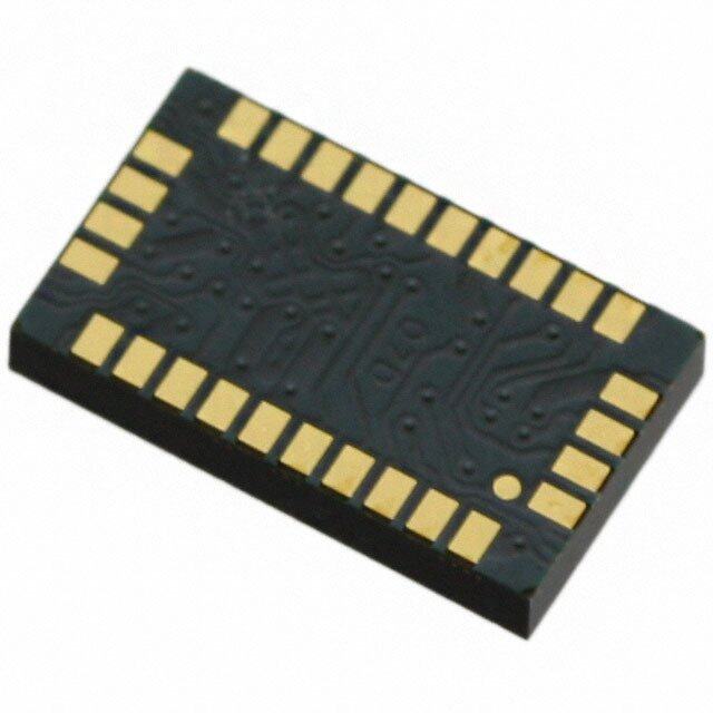
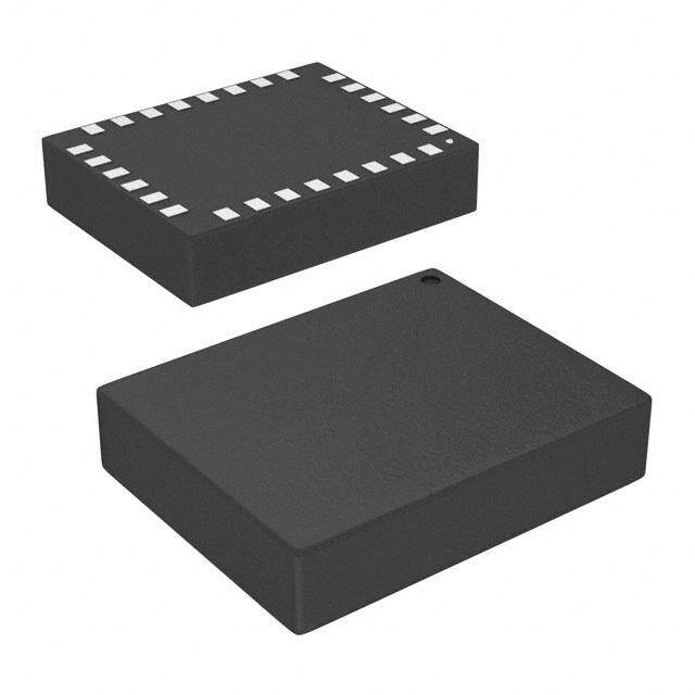
| 产品图片 |
|
| 产品型号 | MPU-9250 |
| rohs | 无铅 / 符合限制有害物质指令(RoHS)规范要求 |
| 产品系列 | - |
| 传感器类型 | 加速计, 陀螺仪, 磁力计 |
| 其它名称 | 1428-1019-1 |
| 标准包装 | 1 |
| 特色产品 | http://www.digikey.cn/product-highlights/zh/mpu9250-9axis-gyroscope-accelerometer-magnetometer/53010 |
| 输出类型 | I²C, SPI |


- 商务部:美国ITC正式对集成电路等产品启动337调查
- 曝三星4nm工艺存在良率问题 高通将骁龙8 Gen1或转产台积电
- 太阳诱电将投资9.5亿元在常州建新厂生产MLCC 预计2023年完工
- 英特尔发布欧洲新工厂建设计划 深化IDM 2.0 战略
- 台积电先进制程称霸业界 有大客户加持明年业绩稳了
- 达到5530亿美元!SIA预计今年全球半导体销售额将创下新高
- 英特尔拟将自动驾驶子公司Mobileye上市 估值或超500亿美元
- 三星加码芯片和SET,合并消费电子和移动部门,撤换高东真等 CEO
- 三星电子宣布重大人事变动 还合并消费电子和移动部门
- 海关总署:前11个月进口集成电路产品价值2.52万亿元 增长14.8%

PDF Datasheet 数据手册内容提取
InvenSense Inc. Document Number: PS-MPU-9250A-01 1745 Technology Drive, San Jose, CA 95110 U.S.A. Tel: +1 (408) 988-7339 Fax: +1 (408) 988-8104 Revision: 1.1 Website: www.invensense.com Release Date: 06/20/2016 MPU-9250 Product Specification Revision 1.1 Page 1 of 42
Document Number: PS-MPU-9250A-01 MPU-9250 Product Specification Revision: 1.1 Release Date: 06/20/2016 CONTENTS 1 DOCUMENT INFORMATION ...................................................................................................................... 4 1.1 REVISION HISTORY .............................................................................................................................. 4 1.2 PURPOSE AND SCOPE .......................................................................................................................... 5 1.3 PRODUCT OVERVIEW ........................................................................................................................... 5 1.4 APPLICATIONS ..................................................................................................................................... 5 2 FEATURES .................................................................................................................................................. 6 2.1 GYROSCOPE FEATURES ....................................................................................................................... 6 2.2 ACCELEROMETER FEATURES ............................................................................................................... 6 2.3 MAGNETOMETER FEATURES................................................................................................................. 6 2.4 ADDITIONAL FEATURES ........................................................................................................................ 6 2.5 MOTIONPROCESSING ........................................................................................................................... 7 3 ELECTRICAL CHARACTERISTICS ........................................................................................................... 8 3.1 GYROSCOPE SPECIFICATIONS .............................................................................................................. 8 3.2 ACCELEROMETER SPECIFICATIONS ....................................................................................................... 9 3.3 MAGNETOMETER SPECIFICATIONS ...................................................................................................... 10 3.4 ELECTRICAL SPECIFICATIONS ............................................................................................................. 11 3.5 I2C TIMING CHARACTERIZATION ......................................................................................................... 15 3.6 SPI TIMING CHARACTERIZATION ......................................................................................................... 16 3.7 ABSOLUTE MAXIMUM RATINGS ........................................................................................................... 18 4 APPLICATIONS INFORMATION .............................................................................................................. 19 4.1 PIN OUT AND SIGNAL DESCRIPTION .................................................................................................... 19 4.2 TYPICAL OPERATING CIRCUIT ............................................................................................................. 20 4.3 BILL OF MATERIALS FOR EXTERNAL COMPONENTS .............................................................................. 20 4.4 BLOCK DIAGRAM ............................................................................................................................... 21 4.5 OVERVIEW ........................................................................................................................................ 22 4.6 THREE-AXIS MEMS GYROSCOPE WITH 16-BIT ADCS AND SIGNAL CONDITIONING ................................ 22 4.7 THREE-AXIS MEMS ACCELEROMETER WITH 16-BIT ADCS AND SIGNAL CONDITIONING ........................ 22 4.8 THREE-AXIS MEMS MAGNETOMETER WITH 16-BIT ADCS AND SIGNAL CONDITIONING ......................... 22 4.9 DIGITAL MOTION PROCESSOR ............................................................................................................ 22 4.10 PRIMARY I2C AND SPI SERIAL COMMUNICATIONS INTERFACES ............................................................ 23 4.11 AUXILIARY I2C SERIAL INTERFACE...................................................................................................... 23 4.12 SELF-TEST ........................................................................................................................................ 24 4.13 MPU-9250 SOLUTION USING I2C INTERFACE ..................................................................................... 25 Page 2 of 42
Document Number: PS-MPU-9250A-01 MPU-9250 Product Specification Revision: 1.1 Release Date: 06/20/2016 4.14 MPU-9250 SOLUTION USING SPI INTERFACE ..................................................................................... 26 4.15 CLOCKING ......................................................................................................................................... 26 4.16 SENSOR DATA REGISTERS ................................................................................................................. 27 4.17 FIFO ................................................................................................................................................ 27 4.18 INTERRUPTS ...................................................................................................................................... 27 4.19 DIGITAL-OUTPUT TEMPERATURE SENSOR .......................................................................................... 27 4.20 BIAS AND LDO .................................................................................................................................. 28 4.21 CHARGE PUMP .................................................................................................................................. 28 4.22 STANDARD POWER MODE .................................................................................................................. 28 4.23 POWER SEQUENCING REQUIREMENTS AND POWER ON RESET ............................................................ 28 5 ADVANCED HARDWARE FEATURES .................................................................................................... 29 6 PROGRAMMABLE INTERRUPTS ............................................................................................................ 30 6.1 WAKE-ON-MOTION INTERRUPT ........................................................................................................... 30 7 DIGITAL INTERFACE ............................................................................................................................... 32 7.1 I2C AND SPI SERIAL INTERFACES ...................................................................................................... 32 7.2 I2C INTERFACE .................................................................................................................................. 32 7.3 I2C COMMUNICATIONS PROTOCOL ..................................................................................................... 32 7.4 I2C TERMS ........................................................................................................................................ 35 7.5 SPI INTERFACE ................................................................................................................................. 36 8 SERIAL INTERFACE CONSIDERATIONS ............................................................................................... 37 8.1 MPU-9250 SUPPORTED INTERFACES ................................................................................................. 37 9 ASSEMBLY ............................................................................................................................................... 38 9.1 ORIENTATION OF AXES ...................................................................................................................... 38 9.2 PACKAGE DIMENSIONS ...................................................................................................................... 38 10 PART NUMBER PACKAGE MARKING ................................................................................................... 40 11 RELIABILITY ............................................................................................................................................. 41 11.1 QUALIFICATION TEST POLICY ............................................................................................................. 41 11.2 QUALIFICATION TEST PLAN ................................................................................................................ 41 12 REFERENCE ............................................................................................................................................. 42 Page 3 of 42
Document Number: PS-MPU-9250A-01 MPU-9250 Product Specification Revision: 1.1 Release Date: 06/20/2016 1 Document Information 1.1 Revision History Revision Revision Description Date 12/18/13 1.0 Initial Release 06/20/16 1.1 Updated Section 4 Page 4 of 42
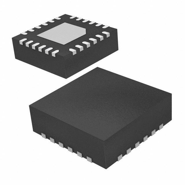
Document Number: PS-MPU-9250A-01 MPU-9250 Product Specification Revision: 1.1 Release Date: 06/20/2016 1.2 Purpose and Scope This document provides a description, specifications, and design related information on the MPU-9250 MotionTracking device. The device is housed in a small 3x3x1mm QFN package. Specifications are subject to change without notice. Final specifications will be updated based upon characterization of production silicon. For references to register map and descriptions of individual registers, please refer to the MPU-9250 Register Map and Register Descriptions document. 1.3 Product Overview MPU-9250 is a multi-chip module (MCM) consisting of two dies integrated into a single QFN package. One die houses the 3-Axis gyroscope and the 3-Axis accelerometer. The other die houses the AK8963 3-Axis magnetometer from Asahi Kasei Microdevices Corporation. Hence, the MPU-9250 is a 9-axis MotionTracking device that combines a 3-axis gyroscope, 3-axis accelerometer, 3-axis magnetometer and a Digital Motion Processor™ (DMP) all in a small 3x3x1mm package available as a pin-compatible upgrade from the MPU- 6515. With its dedicated I2C sensor bus, the MPU-9250 directly provides complete 9-axis MotionFusion™ output. The MPU-9250 MotionTracking device, with its 9-axis integration, on-chip MotionFusion™, and run- time calibration firmware, enables manufacturers to eliminate the costly and complex selection, qualification, and system level integration of discrete devices, guaranteeing optimal motion performance for consumers. MPU-9250 is also designed to interface with multiple non-inertial digital sensors, such as pressure sensors, on its auxiliary I2C port. MPU-9250 features three 16-bit analog-to-digital converters (ADCs) for digitizing the gyroscope outputs, three 16-bit ADCs for digitizing the accelerometer outputs, and three 16-bit ADCs for digitizing the magnetometer outputs. For precision tracking of both fast and slow motions, the parts feature a user-programmable gyroscope full-scale range of ±250, ±500, ±1000, and ±2000°/sec (dps), a user-programmable accelerometer full-scale range of ±2g, ±4g, ±8g, and ±16g, and a magnetometer full-scale range of ±4800µT. Other industry-leading features include programmable digital filters, a precision clock with 1% drift from -40°C to 85°C, an embedded temperature sensor, and programmable interrupts. The device features I2C and SPI serial interfaces, a VDD operating range of 2.4V to 3.6V, and a separate digital IO supply, VDDIO from 1.71V to VDD. Communication with all registers of the device is performed using either I2C at 400kHz or SPI at 1MHz. For applications requiring faster communications, the sensor and interrupt registers may be read using SPI at 20MHz. By leveraging its patented and volume-proven CMOS-MEMS fabrication platform, which integrates MEMS wafers with companion CMOS electronics through wafer-level bonding, InvenSense has driven the package size down to a footprint and thickness of 3x3x1mm, to provide a very small yet high performance low cost package. The device provides high robustness by supporting 10,000g shock reliability. 1.4 Applications Location based services, points of interest, and dead reckoning Handset and portable gaming Motion-based game controllers 3D remote controls for Internet connected DTVs and set top boxes, 3D mice Wearable sensors for health, fitness and sports Page 5 of 42
Document Number: PS-MPU-9250A-01 MPU-9250 Product Specification Revision: 1.1 Release Date: 06/20/2016 2 Features 2.1 Gyroscope Features The triple-axis MEMS gyroscope in the MPU-9250 includes a wide range of features: Digital-output X-, Y-, and Z-Axis angular rate sensors (gyroscopes) with a user-programmable full- scale range of ±250, ±500, ±1000, and ±2000°/sec and integrated 16-bit ADCs Digitally-programmable low-pass filter Gyroscope operating current: 3.2mA Sleep mode current: 8µA Factory calibrated sensitivity scale factor Self-test 2.2 Accelerometer Features The triple-axis MEMS accelerometer in MPU-9250 includes a wide range of features: Digital-output triple-axis accelerometer with a programmable full scale range of ±2g, ±4g, ±8g and ±16g and integrated 16-bit ADCs Accelerometer normal operating current: 450µA Low power accelerometer mode current: 8.4µA at 0.98Hz, 19.8µA at 31.25Hz Sleep mode current: 8µA User-programmable interrupts Wake-on-motion interrupt for low power operation of applications processor Self-test 2.3 Magnetometer Features The triple-axis MEMS magnetometer in MPU-9250 includes a wide range of features: 3-axis silicon monolithic Hall-effect magnetic sensor with magnetic concentrator Wide dynamic measurement range and high resolution with lower current consumption. Output data resolution of 14 bit (0.6µT/LSB) Full scale measurement range is ±4800µT Magnetometer normal operating current: 280µA at 8Hz repetition rate Self-test function with internal magnetic source to confirm magnetic sensor operation on end products 2.4 Additional Features The MPU-9250 includes the following additional features: Auxiliary master I2C bus for reading data from external sensors (e.g. pressure sensor) 3.5mA operating current when all 9 motion sensing axes and the DMP are enabled VDD supply voltage range of 2.4 – 3.6V VDDIO reference voltage for auxiliary I2C devices Smallest and thinnest QFN package for portable devices: 3x3x1mm Minimal cross-axis sensitivity between the accelerometer, gyroscope and magnetometer axes 512 byte FIFO buffer enables the applications processor to read the data in bursts Digital-output temperature sensor User-programmable digital filters for gyroscope, accelerometer, and temp sensor 10,000 g shock tolerant 400kHz Fast Mode I2C for communicating with all registers 1MHz SPI serial interface for communicating with all registers Page 6 of 42
Document Number: PS-MPU-9250A-01 MPU-9250 Product Specification Revision: 1.1 Release Date: 06/20/2016 20MHz SPI serial interface for reading sensor and interrupt registers MEMS structure hermetically sealed and bonded at wafer level RoHS and Green compliant 2.5 MotionProcessing Internal Digital Motion Processing™ (DMP™) engine supports advanced MotionProcessing and low power functions such as gesture recognition using programmable interrupts Low-power pedometer functionality allows the host processor to sleep while the DMP maintains the step count. Page 7 of 42
Document Number: PS-MPU-9250A-01 MPU-9250 Product Specification Revision: 1.1 Release Date: 06/20/2016 3 Electrical Characteristics 3.1 Gyroscope Specifications Typical Operating Circuit of section 4.2, VDD = 2.5V, VDDIO = 2.5V, T =25°C, unless otherwise noted. A PARAMETER CONDITIONS MIN TYP MAX UNITS Full-Scale Range FS_SEL=0 ±250 º/s FS_SEL=1 ±500 º/s FS_SEL=2 ±1000 º/s FS_SEL=3 ±2000 º/s Gyroscope ADC Word Length 16 bits Sensitivity Scale Factor FS_SEL=0 131 LSB/(º/s) FS_SEL=1 65.5 LSB/(º/s) FS_SEL=2 32.8 LSB/(º/s) FS_SEL=3 16.4 LSB/(º/s) Sensitivity Scale Factor Tolerance 25°C ±3 % Sensitivity Scale Factor Variation Over -40°C to +85°C ±4 % Temperature Nonlinearity Best fit straight line; 25°C ±0.1 % Cross-Axis Sensitivity ±2 % Initial ZRO Tolerance 25°C ±5 º/s ZRO Variation Over Temperature -40°C to +85°C ±30 º/s Total RMS Noise DLPFCFG=2 (92 Hz) 0.1 º/s-rms Rate Noise Spectral Density 0.01 º/s/√Hz Gyroscope Mechanical Frequencies 25 27 29 KHz Low Pass Filter Response Programmable Range 5 250 Hz Gyroscope Startup Time From Sleep mode 35 ms Output Data Rate Programmable, Normal mode 4 8000 Hz Table 1 Gyroscope Specifications Page 8 of 42
Document Number: PS-MPU-9250A-01 MPU-9250 Product Specification Revision: 1.1 Release Date: 06/20/2016 3.2 Accelerometer Specifications Typical Operating Circuit of section 4.2, VDD = 2.5V, VDDIO = 2.5V, T =25°C, unless otherwise noted. A PARAMETER CONDITIONS MIN TYP MAX UNITS AFS_SEL=0 ±2 g AFS_SEL=1 ±4 g Full-Scale Range AFS_SEL=2 ±8 g AFS_SEL=3 ±16 g ADC Word Length Output in two’s complement format 16 bits AFS_SEL=0 16,384 LSB/g AFS_SEL=1 8,192 LSB/g Sensitivity Scale Factor AFS_SEL=2 4,096 LSB/g AFS_SEL=3 2,048 LSB/g Initial Tolerance Component-Level ±3 % -40°C to +85°C AFS_SEL=0 Sensitivity Change vs. Temperature ±0.026 %/°C Component-level Nonlinearity Best Fit Straight Line ±0.5 % Cross-Axis Sensitivity ±2 % Zero-G Initial Calibration Tolerance Component-level, X,Y ±60 mg Component-level, Z ±80 mg Zero-G Level Change vs. Temperature -40°C to +85°C ±1.5 mg/°C Noise Power Spectral Density Low noise mode 300 µg/√Hz Total RMS Noise DLPFCFG=2 (94Hz) 8 mg-rms Low Pass Filter Response Programmable Range 5 260 Hz Intelligence Function Increment 4 mg/LSB From Sleep mode 20 ms Accelerometer Startup Time From Cold Start, 1ms V ramp 30 ms DD Low power (duty-cycled) 0.24 500 Hz Output Data Rate Duty-cycled, over temp ±15 % Low noise (active) 4 4000 Hz Table 2 Accelerometer Specifications Page 9 of 42
Document Number: PS-MPU-9250A-01 MPU-9250 Product Specification Revision: 1.1 Release Date: 06/20/2016 3.3 Magnetometer Specifications Typical Operating Circuit of section 4.2, VDD = 2.5V, VDDIO = 2.5V, T =25°C, unless otherwise noted. A PARAMETER CONDITIONS MIN TYP MAX UNITS MAGNETOMETER SENSITIVITY Full-Scale Range ±4800 µT ADC Word Length 14 bits Sensitivity Scale Factor 0.6 µT / LSB ZERO-FIELD OUTPUT Initial Calibration Tolerance ±500 LSB Page 10 of 42
Document Number: PS-MPU-9250A-01 MPU-9250 Product Specification Revision: 1.1 Release Date: 06/20/2016 3.4 Electrical Specifications 3.4.1 D.C. Electrical Characteristics Typical Operating Circuit of section 4.2, VDD = 2.5V, VDDIO = 2.5V, T =25°C, unless otherwise noted. A PARAMETER CONDITIONS MIN TYP MAX Units Notes SUPPLY VOLTAGES VDD 2.4 2.5 3.6 V VDDIO 1.71 1.8 VDD V SUPPLY CURRENTS Normal Mode 9-axis (no DMP), 1 kHz gyro ODR, 4 kHz 3.7 mA accel ODR, 8 Hz mag. repetition rate 6-axis (accel + gyro, no DMP), 1 kHz gyro 3.4 mA ODR, 4 kHz accel ODR 3-axis Gyroscope only (no DMP), 1 kHz ODR 3.2 mA 6-axis (accel + magnetometer, no DMP), 4 730 µA kHz accel ODR, mag. repetition rate = 8 Hz 3-Axis Accelerometer, 4kHz ODR (no DMP) 450 µA 3-axis Magnetometer only (no DMP), 8 Hz 280 µA repetition rate Accelerometer Low Power Mode 0.98 Hz update rate 8.4 µA 1 (DMP, Gyroscope, Magnetometer disabled) 31.25 Hz update rate 19.8 µA 1 Full Chip Idle Mode Supply Current 8 µA TEMPERATURE RANGE Specified Temperature Range Performance parameters are not applicable -40 +85 °C beyond Specified Temperature Range Table 3 D.C. Electrical Characteristics Notes: 1. Accelerometer Low Power Mode supports the following output data rates (ODRs): 0.24, 0.49, 0.98, 1.95, 3.91, 7.81, 15.63, 31.25, 62.50, 125, 250, 500Hz. Supply current for any update rate can be calculated as: Supply Current in µA = Sleep Current + Update Rate * 0.376 Page 11 of 42
Document Number: PS-MPU-9250A-01 MPU-9250 Product Specification Revision: 1.1 Release Date: 06/20/2016 3.4.2 A.C. Electrical Characteristics Typical Operating Circuit of section 4.2, VDD = 2.5V, VDDIO = 2.5V, T =25°C, unless otherwise noted. A Parameter Conditions MIN TYP MAX Units Monotonic ramp. Ramp rate Supply Ramp Time is 10% to 90% of the final 0.1 100 ms value Operating Range Ambient -40 85 °C Sensitivity Untrimmed 333.87 LSB/°C Room Temp Offset 21°C 0 LSB Supply Ramp Time (T ) Valid power-on RESET 0.01 20 100 ms RAMP Start-up time for register read/write From power-up 11 100 ms AD0 = 0 1101000 I2C ADDRESS AD0 = 1 1101001 VIH, High Level Input Voltage 0.7*VDDIO V VIL, Low Level Input Voltage 0.3*VDDIO V CI, Input Capacitance < 10 pF VOH, High Level Output Voltage RLOAD=1MΩ; 0.9*VDDIO V VOL1, LOW-Level Output Voltage RLOAD=1MΩ; 0.1*VDDIO V VOL.INT1, INT Low-Level Output Voltage OPEN=1, 0.3mA sink 0.1 V Current Output Leakage Current OPEN=1 100 nA tINT, INT Pulse Width LATCH_INT_EN=0 50 µs VIL, LOW Level Input Voltage -0.5V 0.3*VDDIO V VIH, HIGH-Level Input Voltage 0.7*VDDIO VDDIO + V 0.5V V , Hysteresis 0.1*VDDIO V hys V , LOW-Level Output Voltage 3mA sink current 0 0.4 V OL IOL, LOW-Level Output Current VOL=0.4V 3 mA V =0.6V 6 mA OL Output Leakage Current 100 nA t , Output Fall Time from V to V C bus capacitance in pf 20+0.1C 250 ns of IHmax ILmax b b VIL, LOW-Level Input Voltage -0.5V 0.3*VDDIO V VIH, HIGH-Level Input Voltage 0.7* VDDIO VDDIO + V 0.5V Vhys, Hysteresis 0.1* VDDIO V VOL1, LOW-Level Output Voltage VDDIO > 2V; 1mA sink 0 0.4 V current VOL3, LOW-Level Output Voltage VDDIO < 2V; 1mA sink 0 0.2* VDDIO V current IOL, LOW-Level Output Current VOL = 0.4V 3 mA VOL = 0.6V 6 mA Output Leakage Current 100 nA tof, Output Fall Time from VIHmax to VILmax Cb bus capacitance in pF 20+0.1Cb 250 ns Fchoice=0,1,2 32 kHz SMPLRT_DIV=0 Fchoice=3; DLPFCFG=0 or 7 8 kHz Sample Rate SMPLRT_DIV=0 Fchoice=3; DLPFCFG=1,2,3,4,5,6; 1 kHz SMPLRT_DIV=0 Clock Frequency Initial Tolerance CLK_SEL=0, 6; 25°C -2 +2 % Page 12 of 42
Document Number: PS-MPU-9250A-01 MPU-9250 Product Specification Revision: 1.1 Release Date: 06/20/2016 CLK_SEL=1,2,3,4,5; 25°C -1 +1 % CLK_SEL=0,6 -10 +10 % Frequency Variation over Temperature CLK_SEL=1,2,3,4,5 ±1 % Table 4 A.C. Electrical Characteristics Page 13 of 42
Document Number: PS-MPU-9250A-01 MPU-9250 Product Specification Revision: 1.1 Release Date: 06/20/2016 3.4.3 Other Electrical Specifications Typical Operating Circuit of section 4.2, VDD = 2.5V, VDDIO = 2.5V, T =25°C, unless otherwise noted. A PARAMETER CONDITIONS MIN TYP MAX Units 100 SPI Operating Frequency, All Low Speed Characterization kHz ±10% Registers Read/Write High Speed Characterization 1 ±10% MHz SPI Operating Frequency, Sensor 20 ±10% MHz and Interrupt Registers Read Only All registers, Fast-mode 400 kHz I2C Operating Frequency All registers, Standard-mode 100 kHz Table 5 Other Electrical Specifications Page 14 of 42
Document Number: PS-MPU-9250A-01 MPU-9250 Product Specification Revision: 1.1 Release Date: 06/20/2016 3.5 I2C Timing Characterization Typical Operating Circuit of section 4.2, VDD = 2.4V to 3.6V, VDDIO = 1.71 to VDD, T =25°C, unless otherwise A noted. Parameters Conditions Min Typical Max Units Notes I2C TIMING I2C FAST-MODE f , SCL Clock Frequency 400 kHz SCL t , (Repeated) START Condition Hold 0.6 µs HD.STA Time t , SCL Low Period 1.3 µs LOW t , SCL High Period 0.6 µs HIGH t , Repeated START Condition Setup 0.6 µs SU.STA Time t , SDA Data Hold Time 0 µs HD.DAT t , SDA Data Setup Time 100 ns SU.DAT t, SDA and SCL Rise Time C bus cap. from 10 to 400pF 20+0.1C 300 ns r b b t, SDA and SCL Fall Time C bus cap. from 10 to 400pF 20+0.1C 300 ns f b b t , STOP Condition Setup Time 0.6 µs SU.STO t , Bus Free Time Between STOP and 1.3 µs BUF START Condition C, Capacitive Load for each Bus Line < 400 pF b t , Data Valid Time 0.9 µs VD.DAT t , Data Valid Acknowledge Time 0.9 µs VD.ACK Table 6 I2C Timing Characteristics Notes: Timing Characteristics apply to both Primary and Auxiliary I2C Bus Based on characterization of 5 parts over temperature and voltage as mounted on evaluation board or in sockets I2C Bus Timing Diagram Page 15 of 42
Document Number: PS-MPU-9250A-01 MPU-9250 Product Specification Revision: 1.1 Release Date: 06/20/2016 3.6 SPI Timing Characterization Typical Operating Circuit of section 4.2, VDD = 2.4V to 3.6V, VDDIO = 1.71V to VDD, T =25°C, unless A otherwise noted. Parameters Conditions Min Typical Max Units Notes SPI TIMING f , SCLK Clock Frequency 1 MHz SCLK t , SCLK Low Period 400 ns LOW t , SCLK High Period 400 ns HIGH t , CS Setup Time 8 ns SU.CS t , CS Hold Time 500 ns HD.CS t , SDI Setup Time 11 ns SU.SDI t , SDI Hold Time 7 ns HD.SDI t , SDO Valid Time C = 20pF 100 ns VD.SDO load t , SDO Hold Time C = 20pF 4 ns HD.SDO load tDIS.SDO, SDO Output Disable Time 50 ns Table 7 SPI Timing Characteristics Notes: 1. Based on characterization of 5 parts over temperature and voltage as mounted on evaluation board or in sockets SPI Bus Timing Diagram 3.6.1 fSCLK = 20MHz Parameters Conditions Min Typical Max Units SPI TIMING f , SCLK Clock Frequency 0.9 20 MHz SCLK t , SCLK Low Period - - ns LOW t , SCLK High Period - - ns HIGH t , CS Setup Time 1 ns SU.CS t , CS Hold Time 1 ns HD.CS Page 16 of 42
Document Number: PS-MPU-9250A-01 MPU-9250 Product Specification Revision: 1.1 Release Date: 06/20/2016 t , SDI Setup Time 0 ns SU.SDI t , SDI Hold Time 1 ns HD.SDI t , SDO Valid Time C = 20pF 25 ns VD.SDO load t , SDO Output Disable Time 25 ns DIS.SDO Table 8 fCLK = 20MHz Note: 1. Based on characterization of 5 parts over temperature and voltage as mounted on evaluation board or in sockets Page 17 of 42
Document Number: PS-MPU-9250A-01 MPU-9250 Product Specification Revision: 1.1 Release Date: 06/20/2016 3.7 Absolute Maximum Ratings Stress above those listed as “Absolute Maximum Ratings” may cause permanent damage to the device. These are stress ratings only and functional operation of the device at these conditions is not implied. Exposure to the absolute maximum ratings conditions for extended periods may affect device reliability. Specification Symbol Conditions MIN MAX Units Supply Voltage V -0.5 4.0 V DD V -0.5 4.0 V DDIO Acceleration Any axis, unpowered, 10,000 g 0.2ms duration Temperature Operating -40 105 °C Storage -40 125 °C ESD Tolerance HBM 2 KV MM 250 V Page 18 of 42
Document Number: PS-MPU-9250A-01 MPU-9250 Product Specification Revision: 1.1 Release Date: 06/20/2016 4 Applications Information 4.1 Pin Out and Signal Description Pin Number Pin Name Pin Description 1 RESV Reserved. Connect to VDDIO. 7 AUX_CL I2C Master serial clock, for connecting to external sensors 8 VDDIO Digital I/O supply voltage 9 AD0 / SDO I2C Slave Address LSB (AD0); SPI serial data output (SDO) 10 REGOUT Regulator filter capacitor connection 11 FSYNC Frame synchronization digital input. Connect to GND if unused. 12 INT Interrupt digital output (totem pole or open-drain) 13 VDD Power supply voltage and Digital I/O supply voltage 18 GND Power supply ground 19 RESV Reserved. Do not connect. 20 RESV Reserved. Connect to GND. 21 AUX_DA I2C master serial data, for connecting to external sensors 22 nCS Chip select (SPI mode only) 23 SCL / SCLK I2C serial clock (SCL); SPI serial clock (SCLK) 24 SDA / SDI I2C serial data (SDA); SPI serial data input (SDI) 2 – 6, 14 - 17 NC Not internally connected. May be used for PCB trace routing. Table 9 Signal Descriptions K A / SDI L / SCL S X_DA SV SV D C C U E E S S n A R R 4 3 2 1 0 9 2 2 2 2 2 1 RESV 1 18 GND NC 2 17 NC NC 3 16 NC MPU-9250 NC 4 15 NC NC 5 14 NC NC 6 13 VDD 7 8 9 10 11 12 L O O T C T AUX_C VDDI AD0/SD REGOU FSYN IN Figure 1 Pin Out Diagram for MPU-9250 3.0x3.0x1.0mm QFN Page 19 of 42
Document Number: PS-MPU-9250A-01 MPU-9250 Product Specification Revision: 1.1 Release Date: 06/20/2016 4.2 Typical Operating Circuit nCS VDDIO SCL SCLK SDA SDA / SDI SCL / SCLK nCS AUX_DA RESV RESV SDI SDA / SDI SCL / SCLK nCS AUX_DA RESV RESV VDDIO VDDIO 24 23 22 21 20 19 24 23 22 21 20 19 RESV 1 18 GND RESV 1 18 GND NC 2 17 NC NC 2 17 NC NC 3 MPU-9250 16 NC NC 3 MPU-9250 16 NC NC 4 15 NC NC 4 15 NC NC 5 14 NC NC 5 14 NC NC 6 13 VDD 2.4 – 3.3VDC NC 6 13 VDD 2.4 – 3.3VDC 7 8 9 10 11 12 C2, 0.1 mF 7 8 9 10 11 12 C2, 0.1 mF 1.8 – 3.3VDC AUX_CL VDDIO AD0/SDO REGOUT FSYNC INT 1.8 – 3.3VDC AUX_CL VDDIO AD0/SDO REGOUT FSYNC INT C3, 10 nF C1, 0.1 mF C3, 10 nF C1, 0.1 mF AD0 SDO (a) (b) Figure 2 MPU-9250 QFN Application Schematic: (a) I2C operation, (b) SPI operation Note that the INT pin should be connected to a GPIO pin on the system processor that is capable of waking the system processor from suspend mode. 4.3 Bill of Materials for External Components Component Label Specification Quantity Regulator Filter Capacitor C1 Ceramic, X7R, 0.1µF ±10%, 2V 1 VDD Bypass Capacitor C2 Ceramic, X7R, 0.1µF ±10%, 4V 1 VDDIO Bypass Capacitor C3 Ceramic, X7R, 10nF ±10%, 4V 1 Table 10 Bill of Materials Page 20 of 42
Document Number: PS-MPU-9250A-01 MPU-9250 Product Specification Revision: 1.1 Release Date: 06/20/2016 4.4 Block Diagram MPU-9250 Self test X Accel ADC Interrupt INT Status Register nCS Steesltf Y Accel ADC Slave I2C and AD0 / SDO SPI Serial FIFO Interface SCL / SCLK Self SDA / SDI test Z Accel ADC User & Config Sig Registers na Master I2C Serial AUX_CL Self l C Serial Interface test X Gyro ADC ond Sensor Interface ByMpuaxss AUX_DA itio Registers n in FSYNC Self g Y Gyro ADC test Digital Motion Processor Self Z Gyro ADC (DMP) test Signal Conditioning Temp Sensor ADC ADC ADC ADC X Y Z Compass Compass Compass Charge Bias & LDOs Pump VDD GND REGOUT VDDIO Page 21 of 42
Document Number: PS-MPU-9250A-01 MPU-9250 Product Specification Revision: 1.1 Release Date: 06/20/2016 4.5 Overview The MPU-9250 is comprised of the following key blocks and functions: Three-axis MEMS rate gyroscope sensor with 16-bit ADCs and signal conditioning Three-axis MEMS accelerometer sensor with 16-bit ADCs and signal conditioning Three-axis MEMS magnetometer sensor with 16-bit ADCs and signal conditioning Digital Motion Processor (DMP) engine Primary I2C and SPI serial communications interfaces Auxiliary I2C serial interface for 3rd party sensors Clocking Sensor Data Registers FIFO Interrupts Digital-Output Temperature Sensor Gyroscope, Accelerometer and Magnetometer Self-test Bias and LDO Charge Pump 4.6 Three-Axis MEMS Gyroscope with 16-bit ADCs and Signal Conditioning The MPU-9250 consists of three independent vibratory MEMS rate gyroscopes, which detect rotation about the X-, Y-, and Z- Axes. When the gyros are rotated about any of the sense axes, the Coriolis Effect causes a vibration that is detected by a capacitive pickoff. The resulting signal is amplified, demodulated, and filtered to produce a voltage that is proportional to the angular rate. This voltage is digitized using individual on-chip 16-bit Analog-to-Digital Converters (ADCs) to sample each axis. The full-scale range of the gyro sensors may be digitally programmed to ±250, ±500, ±1000, or ±2000 degrees per second (dps). The ADC sample rate is programmable from 8,000 samples per second, down to 3.9 samples per second, and user-selectable low- pass filters enable a wide range of cut-off frequencies. 4.7 Three-Axis MEMS Accelerometer with 16-bit ADCs and Signal Conditioning The MPU-9250’s 3-Axis accelerometer uses separate proof masses for each axis. Acceleration along a particular axis induces displacement on the corresponding proof mass, and capacitive sensors detect the displacement differentially. The MPU-9250’s architecture reduces the accelerometers’ susceptibility to fabrication variations as well as to thermal drift. When the device is placed on a flat surface, it will measure 0g on the X- and Y-axes and +1g on the Z-axis. The accelerometers’ scale factor is calibrated at the factory and is nominally independent of supply voltage. Each sensor has a dedicated sigma-delta ADC for providing digital outputs. The full scale range of the digital output can be adjusted to ±2g, ±4g, ±8g, or ±16g. 4.8 Three-Axis MEMS Magnetometer with 16-bit ADCs and Signal Conditioning The 3-axis magnetometer uses highly sensitive Hall sensor technology. The magnetometer portion of the IC incorporates magnetic sensors for detecting terrestrial magnetism in the X-, Y-, and Z- Axes, a sensor driving circuit, a signal amplifier chain, and an arithmetic circuit for processing the signal from each sensor. Each ADC has a 16-bit resolution and a full scale range of ±4800 µT. 4.9 Digital Motion Processor The embedded Digital Motion Processor (DMP) is located within the MPU-9250 and offloads computation of motion processing algorithms from the host processor. The DMP acquires data from accelerometers, Page 22 of 42
Document Number: PS-MPU-9250A-01 MPU-9250 Product Specification Revision: 1.1 Release Date: 06/20/2016 gyroscopes, magnetometers and additional 3rd party sensors, and processes the data. The resulting data can be read from the DMP’s registers, or can be buffered in a FIFO. The DMP has access to one of the MPU’s external pins, which can be used for generating interrupts. This pin (pin 12) should be connected to a pin on the host processor that can wake the host from suspend mode. The purpose of the DMP is to offload both timing requirements and processing power from the host processor. Typically, motion processing algorithms should be run at a high rate, often around 200Hz, in order to provide accurate results with low latency. This is required even if the application updates at a much lower rate; for example, a low power user interface may update as slowly as 5Hz, but the motion processing should still run at 200Hz. The DMP can be used as a tool in order to minimize power, simplify timing, simplify the software architecture, and save valuable MIPS on the host processor for use in the application. 4.10 Primary I2C and SPI Serial Communications Interfaces The MPU-9250 communicates to a system processor using either a SPI or an I2C serial interface. The MPU- 9250 always acts as a slave when communicating to the system processor. The LSB of the of the I2C slave address is set by pin 9 (AD0). 4.11 Auxiliary I2C Serial Interface The MPU-9250 has an auxiliary I2C bus for communicating to off-chip sensors. This bus has two operating modes: I2C Master Mode: The MPU-9250 acts as a master to any external sensors connected to the auxiliary I2C bus Pass-Through Mode: The MPU-9250 directly connects the primary and auxiliary I2C buses together, allowing the system processor to directly communicate with any external sensors. Note: AUX_DA and AUX_CL should be left unconnected if the Auxiliary I2C mode is not used. Auxiliary I2C Bus Modes of Operation: I2C Master Mode: Allows the MPU-9250 to directly access the data registers of external digital sensors, such as a magnetometer. In this mode, the MPU-9250 directly obtains data from auxiliary sensors without intervention from the system applications processor. For example, In I2C Master mode, the MPU-9250 can be configured to perform burst reads, returning the following data from a magnetometer: X magnetometer data (2 bytes) Y magnetometer data (2 bytes) Z magnetometer data (2 bytes) The I2C Master can be configured to read up to 24 bytes from up to 4 auxiliary sensors. A fifth sensor can be configured to work single byte read/write mode. Pass-Through Mode: Allows an external system processor to act as master and directly communicate to the external sensors connected to the auxiliary I2C bus pins (AUX_DA and AUX_CL). In this mode, the auxiliary I2C bus control logic (3rd party sensor interface block) of the MPU-9250 is disabled, and the auxiliary I2C pins AUX_DA and AUX_CL are connected to the main I2C bus through analog switches internally. Page 23 of 42
Document Number: PS-MPU-9250A-01 MPU-9250 Product Specification Revision: 1.1 Release Date: 06/20/2016 Pass-Through mode is useful for configuring the external sensors, or for keeping the MPU-9250 in a low-power mode when only the external sensors are used. In this mode, the system processor can still access MPU-9250 data through the I2C interface. Pass-Through mode is also used to access the AK8963 magnetometer directly from the host. In this configuration the slave address for the AK8963 is 0X0C or 12 decimal. Auxiliary I2C Bus IO Logic Levels For MPU-9250, the logic level of the auxiliary I2C bus is VDDIO. For further information regarding the MPU- 9250 logic levels, please refer to Section 10.2. 4.12 Self-Test Please refer to the register map document for more details on self-test. Self-test allows for the testing of the mechanical and electrical portions of the sensors. The self-test for each measurement axis can be activated by means of the gyroscope and accelerometer self-test registers (registers 13 to 16). When the self-test is activated, the electronics cause the sensors to be actuated and produce an output signal. The output signal is used to observe the self-test response. The self-test response is defined as follows: Self-test response = Sensor output with self-test enabled – Sensor output without self-test enabled When the value of the self-test response is within the appropriate limits, the part has passed self-test. When the self-test response exceeds the appropriate values, the part is deemed to have failed self-test. It is recommended to use InvenSense MotionApps software for executing self-test. Further details, including the self-test limits are included in the MPU-9250 Self-Test applications note available from InvenSense. Page 24 of 42
Document Number: PS-MPU-9250A-01 MPU-9250 Product Specification Revision: 1.1 Release Date: 06/20/2016 4.13 MPU-9250 Solution Using I2C Interface In the figure below, the system processor is an I2C master to the MPU-9250. In addition, the MPU-9250 is an I2C master to the optional external 3rd party sensor. The MPU-9250 has limited capabilities as an I2C Master, and depends on the system processor to manage the initial configuration of any auxiliary sensors. The MPU- 9250 has an interface bypass multiplexer, which connects the system processor I2C bus (SDA and SCL) directly to the auxiliary sensor I2C bus (AUX_DA and AUX_CL). Once the auxiliary sensors have been configured by the system processor, the interface bypass multiplexer should be disabled so that the MPU-9250 auxiliary I2C master can take control of the sensor I2C bus and gather data from the auxiliary sensors. The INT pin should be connected to a GPIO on the system processor that can wake the system from suspend mode. Interrupt INT Status Register I2C Processor Bus: for reading all sensor data from MPU and for configuring external sensors (i.e. MPU-9250 compass in this example) AD0 Slave I2C VDD or GND or SPI SCL SCL Serial System Interface SDA/SDI SDA Processor FIFO Sensor I2C Bus: for configuring and reading User & Config from external sensors Registers Optional Sensor AUX_CL SCL RSeegnissoterr MInaStseetrerfiraa cIl2 eC InBtyMeprufaaxscse AUX_DA SDA 3srde npsaortry Factory Calibration Digital Motion Processor (DMP) Interface bypass mux allows direct configuration of compass by system processor Bias & LDOs VDD GND REGOUT VDDIO Page 25 of 42
Document Number: PS-MPU-9250A-01 MPU-9250 Product Specification Revision: 1.1 Release Date: 06/20/2016 4.14 MPU-9250 Solution Using SPI Interface In the figure below, the system processor is a SPI master to the MPU-9250. The CS, SDO, SCLK, and SDI signals are used for SPI communications. Because these SPI pins are shared with the I2C slave pins, the system processor cannot access the auxiliary I2C bus through the interface bypass multiplexer, which connects the processor I2C interface pins to the sensor I2C interface pins. Since the MPU-9250 has limited capabilities as an I2C Master, and depends on the system processor to manage the initial configuration of any auxiliary sensors, another method must be used for programming the sensors on the auxiliary sensor I2C bus (AUX_DA and AUX_CL). When using SPI communications between the MPU-9250 and the system processor, configuration of devices on the auxiliary I2C sensor bus can be achieved by using I2C Slaves 0-4 to perform read and write transactions on any device and register on the auxiliary I2C bus. The I2C Slave 4 interface can be used to perform only single byte read and write transactions. Once the external sensors have been configured, the MPU-9250 can perform single or multi-byte reads using the sensor I2C bus. The read results from the Slave 0-3 controllers can be written to the FIFO buffer as well as to the external sensor registers. The INT pin should be connected to a GPIO on the system processor capable of waking the processor from suspend For further information regarding the control of the MPU-9250’s auxiliary I2C interface, please refer to the MPU- 9250 Register Map and Register Descriptions document. Interrupt Status Processor SPI Bus: for reading all Register INT data from MPU and for configuring MPU and external sensors nCS nCS MPU-9250 SDO SDI Slave I2C System or SPI SCLK SCLK Processor Serial Interface SDI SDO FIFO Sensor I2C Bus: for configuring and Config reading data from Register external sensors Optional RSeegnissoterr MInSaStseeetnrerfsiraao cIlr2 e C InBtyMeprufaaxscse AAUUXX__CDLA SSCDLA 3srde npsaortry Factory Calibration Digital Motion Processor (DMP) I2C Master performs read and write transactions on Sensor I2C bus. Bias & LDOs VDD GND REGOUT VDDIO 4.15 Clocking The MPU-9250 has a flexible clocking scheme, allowing a variety of internal clock sources to be used for the internal synchronous circuitry. This synchronous circuitry includes the signal conditioning and ADCs, the DMP, and various control circuits and registers. An on-chip PLL provides flexibility in the allowable inputs for generating this clock. Page 26 of 42
Document Number: PS-MPU-9250A-01 MPU-9250 Product Specification Revision: 1.1 Release Date: 06/20/2016 Allowable internal sources for generating the internal clock are: An internal relaxation oscillator Any of the X, Y, or Z gyros (MEMS oscillators with a variation of ±1% over temperature) Selection of the source for generating the internal synchronous clock depends on the requirements for power consumption and clock accuracy. These requirements will most likely vary by mode of operation. For example, in one mode, where the biggest concern is power consumption, the user may wish to operate the Digital Motion Processor of the MPU-9250 to process accelerometer data, while keeping the gyros off. In this case, the internal relaxation oscillator is a good clock choice. However, in another mode, where the gyros are active, selecting the gyros as the clock source provides for a more accurate clock source. Clock accuracy is important, since timing errors directly affect the distance and angle calculations performed by the Digital Motion Processor (and by extension, by any processor). There are also start-up conditions to consider. When the MPU-9250 first starts up, the device uses its internal clock until programmed to operate from another source. This allows the user, for example, to wait for the MEMS oscillators to stabilize before they are selected as the clock source. 4.16 Sensor Data Registers The sensor data registers contain the latest gyroscope, accelerometer, magnetometer, auxiliary sensor, and temperature measurement data. They are read-only registers, and are accessed via the serial interface. Data from these registers may be read anytime. 4.17 FIFO The MPU-9250 contains a 512-byte FIFO register that is accessible via the Serial Interface. The FIFO configuration register determines which data is written into the FIFO. Possible choices include gyro data, accelerometer data, temperature readings, auxiliary sensor readings, and FSYNC input. A FIFO counter keeps track of how many bytes of valid data are contained in the FIFO. The FIFO register supports burst reads. The interrupt function may be used to determine when new data is available. For further information regarding the FIFO, please refer to the MPU-9250 Register Map and Register Descriptions document. 4.18 Interrupts Interrupt functionality is configured via the Interrupt Configuration register. Items that are configurable include the INT pin configuration, the interrupt latching and clearing method, and triggers for the interrupt. Items that can trigger an interrupt are (1) Clock generator locked to new reference oscillator (used when switching clock sources); (2) new data is available to be read (from the FIFO and Data registers); (3) accelerometer event interrupts; and (4) the MPU-9250 did not receive an acknowledge from an auxiliary sensor on the secondary I2C bus. The interrupt status can be read from the Interrupt Status register. The INT pin should be connected to a pin on the host processor capable of waking that processor from suspend. For further information regarding interrupts, please refer to the MPU-9250 Register Map and Register Descriptions document. 4.19 Digital-Output Temperature Sensor An on-chip temperature sensor and ADC are used to measure the MPU-9250 die temperature. The readings from the ADC can be read from the FIFO or the Sensor Data registers. Page 27 of 42
Document Number: PS-MPU-9250A-01 MPU-9250 Product Specification Revision: 1.1 Release Date: 06/20/2016 4.20 Bias and LDO The bias and LDO section generates the internal supply and the reference voltages and currents required by the MPU-9250. Its two inputs are an unregulated VDD and a VDDIO logic reference supply voltage. The LDO output is bypassed by a capacitor at REGOUT. For further details on the capacitor, please refer to the Bill of Materials for External Components. 4.21 Charge Pump An on-chip charge pump generates the high voltage required for the MEMS oscillators. 4.22 Standard Power Mode The following table lists the user-accessible power modes for MPU-9250. Mode Name Gyro Accel Magnetometer DMP 1 Sleep Mode Off Off Off Off 2 Standby Mode Drive On Off Off Off 3 Low-Power Accelerometer Mode Off Duty-Cycled Off On or Off 4 Low-Noise Accelerometer Mode Off On Off On or Off 5 Gyroscope Mode On Off Off On or Off 6 Magnetometer Mode Off Off On On or Off 7 Accel + Gyro Mode On On Off On or Off 8 Accel + Magnetometer Mode Off On On On or Off 9 9-Axis Mode On On On On or Off Notes: 1. Power consumption for individual modes can be found in Electrical Characteristics section. 4.23 Power Sequencing Requirements and Power on Reset During power up and in normal operation, VDDIO must not exceed VDD. During power up, VDD and VDDIO must be monotonic ramps. As stated in Table 4, the minimum VDD rise time is 0.1ms and the maximum rise time is 100 ms. Valid gyroscope data is available 35 ms (typical) after VDD has risen to its final voltage from a cold start and valid accelerometer data is available 30 ms (typical) after VDD has risen to its final voltage assuming a 1ms VDD ramp from cold start. Magnetometer data is valid 7.3ms (typical) after VDD has risen to its final voltage value from a cold start. Page 28 of 42
Document Number: PS-MPU-9250A-01 MPU-9250 Product Specification Revision: 1.1 Release Date: 06/20/2016 5 Advanced Hardware Features The MPU-9250 includes advanced hardware features that can be enabled and disabled through simple hardware register settings. The advanced hardware features are not initially enabled after device power up. These features must be individually enabled and configured. These advanced hardware features enable the following motion-based functions without using an external microprocessor: Low Power Quaternion (3-Axis Gyro & 6-Axis Gyro + Accel) Android Orientation (A low-power implementation of Android’s screen rotation algorithm) Tap (detects the tap gesture) Pedometer Significant Motion Detection To ensure significant motion detection can operate properly, the INT pin should be connected to a GPIO pin on the host processor that can wake that processor from suspend mode. Note: Android Orientation is compliant to the Ice Cream Sandwich definition of the function. For further details on advanced hardware features please refer to the MPU-9250 Register Map. Page 29 of 42
Document Number: PS-MPU-9250A-01 MPU-9250 Product Specification Revision: 1.1 Release Date: 06/20/2016 6 Programmable Interrupts The MPU-9250 has a programmable interrupt system which can generate an interrupt signal on the INT pin. Status flags indicate the source of an interrupt. Interrupt sources may be enabled and disabled individually. Table of Interrupt Sources Interrupt Name Module Motion Detection Motion FIFO Overflow FIFO Data Ready Sensor Registers I2C Master errors: Lost Arbitration, NACKs I2C Master I2C Slave 4 I2C Master For information regarding the interrupt enable/disable registers and flag registers, please refer to the MPU- 9250 Register Map and Register Descriptions document. Some interrupt sources are explained below. 6.1 Wake-on-Motion Interrupt The MPU-9250 provides motion detection capability. A qualifying motion sample is one where the high passed sample from any axis has an absolute value exceeding a user-programmable threshold. The following flowchart explains how to configure the Wake-on-Motion Interrupt. For further details on individual registers, please refer to the MPU-9250 Registers Map and Registers Description document. In order to properly enable motion interrupts, the INT pin should be connected to a GPIO on the system processor that is capable of waking up the system processor. Page 30 of 42
Document Number: PS-MPU-9250A-01 MPU-9250 Product Specification Revision: 1.1 Release Date: 06/20/2016 Configuration Wake-on-Motion Interrupt using low power Accelmode Make Sure Accelis running: • In PWR_MGMT_1 (0x6B) make CYCLE =0, SLEEP = 0 and STANDBY = 0 • In PWR_MGMT_2 (0x6C) set DIS_XA, DIS_YA, DIS_ZA = 0 and DIS_XG, DIS_YG, DIS_ZG = 1 SeSt eAt cAccecleLl PLFP Fse stettitningg t too 118844 HHzz BBaannddwwiditdht:h : • In ACCEL_CONFIG 2 (0x1D) set ACCEL_FCHOICE_B = 0 and A_DLPFCFG[2:0]=1(b001) In ACCEL_CONFIG 2 (0x1D) set ACCEL_FCHOICE_B = 1 and A_DLPFCFG[2:]=1(b001) Enable Motion Interrupt: • In INT_ENABLE (0x38), set the whole register to 0x40 to enable motion interrupt only. Enable AccelHardware Intelligence: • In MOT_DETECT_CTRL (0x69), set ACCEL_INTEL_EN = 1 and ACCEL_INTEL_MODE = 1 Set Motion Threshold: • In WOM_THR (0x1F), set the WOM_Threshold[7:0] to 1~255 LSBs (0~1020mg) Set Frequency of Wake-up: • In LP_ACCEL_ODR (0x1E), set Lposc_clksel[3:0] = 0.24Hz ~ 500Hz Enable Cycle Mode (AccelLow Power Mode): • In PWR_MGMT_1 (0x6B) make CYCLE =1 Motion Interrupt Configuration Completed Figure 3. Wake-on-Motion Interrupt Configuration Page 31 of 42
Document Number: PS-MPU-9250A-01 MPU-9250 Product Specification Revision: 1.1 Release Date: 06/20/2016 7 Digital Interface 7.1 I2C and SPI Serial Interfaces The internal registers and memory of the MPU-9250 can be accessed using either I2C at 400 kHz or SPI at 1MHz. SPI operates in four-wire mode. Serial Interface Pin Number Pin Name Pin Description 8 VDDIO Digital I/O supply voltage. 9 AD0 / SDO I2C Slave Address LSB (AD0); SPI serial data output (SDO) 23 SCL / SCLK I2C serial clock (SCL); SPI serial clock (SCLK) 24 SDA / SDI I2C serial data (SDA); SPI serial data input (SDI) Note: To prevent switching into I2C mode when using SPI, the I2C interface should be disabled by setting the I2C_IF_DIS configuration bit. Setting this bit should be performed immediately after waiting for the time specified by the “Start-Up Time for Register Read/Write” in Section 6.3. For further information regarding the I2C_IF_DIS bit, please refer to the MPU-9250 Register Map and Register Descriptions document. 7.2 I2C Interface I2C is a two-wire interface comprised of the signals serial data (SDA) and serial clock (SCL). In general, the lines are open-drain and bi-directional. In a generalized I2C interface implementation, attached devices can be a master or a slave. The master device puts the slave address on the bus, and the slave device with the matching address acknowledges the master. The MPU-9250 always operates as a slave device when communicating to the system processor, which thus acts as the master. SDA and SCL lines typically need pull-up resistors to VDD. The maximum bus speed is 400 kHz. The slave address of the MPU-9250 is b110100X which is 7 bits long. The LSB bit of the 7 bit address is determined by the logic level on pin AD0. This allows two MPU-9250s to be connected to the same I2C bus. When used in this configuration, the address of the one of the devices should be b1101000 (pin AD0 is logic low) and the address of the other should be b1101001 (pin AD0 is logic high). 7.3 I2C Communications Protocol START (S) and STOP (P) Conditions Communication on the I2C bus starts when the master puts the START condition (S) on the bus, which is defined as a HIGH-to-LOW transition of the SDA line while SCL line is HIGH (see figure below). The bus is considered to be busy until the master puts a STOP condition (P) on the bus, which is defined as a LOW to HIGH transition on the SDA line while SCL is HIGH (see figure below). Additionally, the bus remains busy if a repeated START (Sr) is generated instead of a STOP condition. Page 32 of 42
Document Number: PS-MPU-9250A-01 MPU-9250 Product Specification Revision: 1.1 Release Date: 06/20/2016 SDA SCL S P START condition STOP condition START and STOP Conditions Data Format / Acknowledge I2C data bytes are defined to be 8-bits long. There is no restriction to the number of bytes transmitted per data transfer. Each byte transferred must be followed by an acknowledge (ACK) signal. The clock for the acknowledge signal is generated by the master, while the receiver generates the actual acknowledge signal by pulling down SDA and holding it low during the HIGH portion of the acknowledge clock pulse. If a slave is busy and cannot transmit or receive another byte of data until some other task has been performed, it can hold SCL LOW, thus forcing the master into a wait state. Normal data transfer resumes when the slave is ready, and releases the clock line (refer to the following figure). DATA OUTPUT BY TRANSMITTER (SDA) not acknowledge DATA OUTPUT BY RECEIVER (SDA) acknowledge SCL FROM 1 2 8 9 MASTER clock pulse for START acknowledgement condition Acknowledge on the I2C Bus Page 33 of 42
Document Number: PS-MPU-9250A-01 MPU-9250 Product Specification Revision: 1.1 Release Date: 06/20/2016 Communications After beginning communications with the START condition (S), the master sends a 7-bit slave address followed by an 8th bit, the read/write bit. The read/write bit indicates whether the master is receiving data from or is writing to the slave device. Then, the master releases the SDA line and waits for the acknowledge signal (ACK) from the slave device. Each byte transferred must be followed by an acknowledge bit. To acknowledge, the slave device pulls the SDA line LOW and keeps it LOW for the high period of the SCL line. Data transmission is always terminated by the master with a STOP condition (P), thus freeing the communications line. However, the master can generate a repeated START condition (Sr), and address another slave without first generating a STOP condition (P). A LOW to HIGH transition on the SDA line while SCL is HIGH defines the stop condition. All SDA changes should take place when SCL is low, with the exception of start and stop conditions. SDA SCL 1 – 7 8 9 1 – 7 8 9 1 – 7 8 9 S P START ADDRESS R/W ACK DATA ACK DATA ACK STOP condition condition Complete I2C Data Transfer To write the internal MPU-9250 registers, the master transmits the start condition (S), followed by the I2C address and the write bit (0). At the 9th clock cycle (when the clock is high), the MPU-9250 acknowledges the transfer. Then the master puts the register address (RA) on the bus. After the MPU-9250 acknowledges the reception of the register address, the master puts the register data onto the bus. This is followed by the ACK signal, and data transfer may be concluded by the stop condition (P). To write multiple bytes after the last ACK signal, the master can continue outputting data rather than transmitting a stop signal. In this case, the MPU- 9250 automatically increments the register address and loads the data to the appropriate register. The following figures show single and two-byte write sequences. Single-Byte Write Sequence Master S AD+W RA DATA P Slave ACK ACK ACK Burst Write Sequence Master S AD+W RA DATA DATA P Slave ACK ACK ACK ACK Page 34 of 42
Document Number: PS-MPU-9250A-01 MPU-9250 Product Specification Revision: 1.1 Release Date: 06/20/2016 To read the internal MPU-9250 registers, the master sends a start condition, followed by the I2C address and a write bit, and then the register address that is going to be read. Upon receiving the ACK signal from the MPU- 9250, the master transmits a start signal followed by the slave address and read bit. As a result, the MPU- 9250 sends an ACK signal and the data. The communication ends with a not acknowledge (NACK) signal and a stop bit from master. The NACK condition is defined such that the SDA line remains high at the 9th clock cycle. The following figures show single and two-byte read sequences. Single-Byte Read Sequence Master S AD+W RA S AD+R NACK P Slave ACK ACK ACK DATA Burst Read Sequence Master S AD+W RA S AD+R ACK NACK P Slave ACK ACK ACK DATA DATA 7.4 I2C Terms Signal Description S Start Condition: SDA goes from high to low while SCL is high AD Slave I2C address W Write bit (0) R Read bit (1) ACK Acknowledge: SDA line is low while the SCL line is high at the 9th clock cycle NACK Not-Acknowledge: SDA line stays high at the 9th clock cycle RA MPU-9250 internal register address DATA Transmit or received data P Stop condition: SDA going from low to high while SCL is high Page 35 of 42
Document Number: PS-MPU-9250A-01 MPU-9250 Product Specification Revision: 1.1 Release Date: 06/20/2016 7.5 SPI Interface SPI is a 4-wire synchronous serial interface that uses two control lines and two data lines. The MPU-9250 always operates as a Slave device during standard Master-Slave SPI operation. With respect to the Master, the Serial Clock output (SCLK), the Serial Data Output (SDO) and the Serial Data Input (SDI) are shared among the Slave devices. Each SPI slave device requires its own Chip Select (CS) line from the master. CS goes low (active) at the start of transmission and goes back high (inactive) at the end. Only one CS line is active at a time, ensuring that only one slave is selected at any given time. The CS lines of the non-selected slave devices are held high, causing their SDO lines to remain in a high-impedance (high-z) state so that they do not interfere with any active devices. SPI Operational Features 1. Data is delivered MSB first and LSB last 2. Data is latched on the rising edge of SCLK 3. Data should be transitioned on the falling edge of SCLK 4. The maximum frequency of SCLK is 1MHz 5. SPI read and write operations are completed in 16 or more clock cycles (two or more bytes). The first byte contains the SPI Address, and the following byte(s) contain(s) the SPI data. The first bit of the first byte contains the Read/Write bit and indicates the Read (1) or Write (0) operation. The following 7 bits contain the Register Address. In cases of multiple-byte Read/Writes, data is two or more bytes: SPI Address format MSB LSB R/W A6 A5 A4 A3 A2 A1 A0 SPI Data format MSB LSB D7 D6 D5 D4 D3 D2 D1 D0 6. Supports Single or Burst Read/Writes. SCLK SDI SPI Master SDO SPI Slave 1 /CS1 /CS /CS2 SCLK SDI SDO SPI Slave 2 /CS Typical SPI Master / Slave Configuration Page 36 of 42
Document Number: PS-MPU-9250A-01 MPU-9250 Product Specification Revision: 1.1 Release Date: 06/20/2016 8 Serial Interface Considerations 8.1 MPU-9250 Supported Interfaces The MPU-9250 supports I2C communications on both its primary (microprocessor) serial interface and its auxiliary interface. The MPU-9250’s I/O logic levels are set to be VDDIO. The figure below depicts a sample circuit of MPU-9250 with a third party sensor attached to the auxiliary I2C bus. It shows the relevant logic levels and voltage connections. Note: Actual configuration will depend on the auxiliary sensors used. VDDIO VDD_IO (0V - VDDIO) SYSTEM BUS System VDD Processor IO VDDIO (0V - VDDIO) VDD INT VDDIO (0V - VDDIO) SDA (0V - VDDIO) SCL (0V - VDDIO) FSYNC VDDIO MPU-9250 VDD_IO VDDIO (0V, VDDIO) CS (0V - VDDIO) 3rd Party (0V - VDDIO) AUX_DA SDA INT 1 Sensor (0V, VDDIO) AD0 AUX_CL (0V - VDDIO) SCL INT 2 (0V - VDDIO) (0V, VDDIO) SA0 I/O Levels and Connections Page 37 of 42
Document Number: PS-MPU-9250A-01 MPU-9250 Product Specification Revision: 1.1 Release Date: 06/20/2016 9 Assembly This section provides general guidelines for assembling InvenSense Micro Electro-Mechanical Systems (MEMS) devices packaged in quad flat no-lead package (QFN) surface mount integrated circuits. 9.1 Orientation of Axes The diagram below shows the orientation of the axes of sensitivity and the polarity of rotation. Note the pin 1 identifier (•) in the figure. +Z +Z +Y MPU-9250 +Y +X +X Figure 4. Orientation of Axes of Sensitivity and Polarity of Rotation for Accelerometer and Gyroscope +X MPU-9250 +Y +Z Figure 5. Orientation of Axes of Sensitivity for Compass 9.2 Package Dimensions 24 Lead QFN (3x3x1) mm NiPdAu Lead-frame finish Page 38 of 42
Document Number: PS-MPU-9250A-01 MPU-9250 Product Specification Revision: 1.1 Release Date: 06/20/2016 DIMENSIONS IN MILLIMETERS SYMBOLS DESCRIPTION MIN NOM MAX A Package thickness 0.95 1.00 1.05 A1 Lead finger (pad) seating height 0.00 0.02 0.05 b Lead finger (pad) width 0.15 0.20 0.25 c Lead frame (pad) height --- 0.15 REF --- D Package width 2.90 3.00 3.10 D2 Exposed pad width 1.65 1.70 1.75 E Package length 2.90 3.00 3.10 E2 Exposed pad length 1.49 1.54 1.59 e Lead finger-finger (pad-pad) pitch --- 0.40 --- f (e-b) Lead-lead (Pad-Pad) space 0.15 0.20 0.25 K Lead (pad) to Exposed Pad Space --- 0.35 REF --- L Lead (pad) length 0.25 0.30 0.35 R Lead (pad) corner radius 0.075 REF --- Corner lead (pad) outer radius to corner s lead outer radius --- 0.25 REF --- y 0.00 --- 0.075 Page 39 of 42
Document Number: PS-MPU-9250A-01 MPU-9250 Product Specification Revision: 1.1 Release Date: 06/20/2016 10 Part Number Package Marking The part number package marking for MPU-9250 devices is summarized below: Part Number Part Number Package Marking MPU-9250 MP92 Page 40 of 42
Document Number: PS-MPU-9250A-01 MPU-9250 Product Specification Revision: 1.1 Release Date: 06/20/2016 11 Reliability 11.1 Qualification Test Policy InvenSense’s products complete a Qualification Test Plan before being released to production. The Qualification Test Plan for the MPU-9250 followed the JEDEC JESD 47I Standard, “Stress-Test-Driven Qualification of Integrated Circuits,” with the individual tests described below. 11.2 Qualification Test Plan Accelerated Life Tests TEST Method/Condition Lot Sample Acc / Quantity / Lot Reject Criteria (HTOL/LFR) JEDEC JESD22-A108D 3 77 (0/1) High Temperature Operating Life Dynamic, 3.63V biased, Tj>125°C [read-points: 168, 500, 1000 hours] (HAST) JEDEC JESD22-A118A 3 77 (0/1) Highly Accelerated Stress Test (1) Condition A, 130°C, 85%RH, 33.3 psia., unbiased [read-point: 96 hours] (HTS) JEDEC JESD22-A103D 3 77 (0/1) High Temperature Storage Life Condition A, 125°C Non-Bias Bake [read-points: 168, 500, 1000 hours] Device Component Level Tests TEST Method/Condition Lot Sample Acc / Quantity / Lot Reject Criteria (ESD-HBM) JEDEC JS-001-2012 1 3 (0/1) ESD-Human Body Model (2KV) (ESD-MM) JEDEC JESD22-A115C 1 3 (0/1) ESD-Machine Model (250V) (ESD-CDM) JEDEC JESD22-C101E 1 3 (0/1) ESD-Charged Device Model (500V) (LU) JEDEC JESD-78D 1 6 (0/1) Latch Up Class II (2), 125°C; ±100mA 1.5X Vdd Over-voltage (MS) JEDEC JESD22-B104C, Mil-Std-883, Method 3 5 (0/1) Mechanical Shock 2002.5 Cond. E, 10,000g’s, 0.2ms, ±X, Y, Z – 6 directions, 5 times/direction (VIB) JEDEC JESD22-B103B 1 5 (0/1) Vibration Variable Frequency (random), Cond. B, 5-500Hz, X, Y, Z – 4 times/direction (TC) JEDEC JESD22-A104D 3 77 (0/1) Temperature Cycling (1) Condition G [-40°C to +125°C], Soak Mode 2 [5’] [read-Point: 1000 cycles] (1) Tests are preceded by MSL3 Preconditioning in accordance with JEDEC JESD22-A113F Page 41 of 42
Document Number: PS-MPU-9250A-01 MPU-9250 Product Specification Revision: 1.1 Release Date: 06/20/2016 12 Reference Please refer to “InvenSense MEMS Handling Application Note (AN-IVS-0002A-00)” for the following information: Manufacturing Recommendations o Assembly Guidelines and Recommendations o PCB Design Guidelines and Recommendations o MEMS Handling Instructions o ESD Considerations o Reflow Specification o Storage Specifications o Package Marking Specification o Tape & Reel Specification o Reel & Pizza Box Label o Packaging o Representative Shipping Carton Label Compliance o Environmental Compliance o DRC Compliance o Compliance Declaration Disclaimer This information furnished by InvenSense is believed to be accurate and reliable. However, no responsibility is assumed by InvenSense for its use, or for any infringements of patents or other rights of third parties that may result from its use. Specifications are subject to change without notice. InvenSense reserves the right to make changes to this product, including its circuits and software, in order to improve its design and/or performance, without prior notice. InvenSense makes no warranties, neither expressed nor implied, regarding the information and specifications contained in this document. InvenSense assumes no responsibility for any claims or damages arising from information contained in this document, or from the use of products and services detailed therein. This includes, but is not limited to, claims or damages based on the infringement of patents, copyrights, mask work and/or other intellectual property rights. Certain intellectual property owned by InvenSense and described in this document is patent protected. No license is granted by implication or otherwise under any patent or patent rights of InvenSense. This publication supersedes and replaces all information previously supplied. Trademarks that are registered trademarks are the property of their respective companies. InvenSense sensors should not be used or sold in the development, storage, production or utilization of any conventional or mass-destructive weapons or for any other weapons or life threatening applications, as well as in any other life critical applications such as medical equipment, transportation, aerospace and nuclear instruments, undersea equipment, power plant equipment, disaster prevention and crime prevention equipment. ©2014 InvenSense, Inc. All rights reserved. InvenSense, MotionTracking, MotionProcessing, MotionProcessor, MotionFusion, MotionApps, DMP, and the InvenSense logo are trademarks of InvenSense, Inc. Other company and product names may be trademarks of the respective companies with which they are associated. ©2014 InvenSense, Inc. All rights reserved. Page 42 of 42
Mouser Electronics Authorized Distributor Click to View Pricing, Inventory, Delivery & Lifecycle Information: T DK: MPU-9250